TECHNICAL FIELD
The disclosure relates to a display device and a method for manufacturing the same.
BACKGROUND ART
In recent years, a self-luminous type organic electroluminescence (hereinafter also referred to as EL) display device using an organic EL element has attracted attention as a display device that can replace liquid crystal display devices. As the organic EL display device, an organic EL display device having flexibility in which an organic EL element, a variety of films, and the like are layered on a flexible resin substrate, has been proposed.
For example, PTL 1 discloses a flexible display with a redundancy design including a pair of sinusoidal metal wiring lines being out of phase by approximately 180 degrees from each other.
CITATION LIST
Patent Literature
SUMMARY
Technical Problem
In a case where, in a flexible display device, wiring lines are formed by a refractory metal such as molybdenum and titanium, in a case where a metal film formed of a refractory metal is formed on a gate insulating film, for example, a crack may occur in the gate insulating film due to a high stress generated in the metal film. As a result, since the wiring lines formed by patterning the metal film formed of the refractory metal break and moisture penetrates through the crack formed in the gate insulating film, a production yield is reduced or reliability of the display device is reduced. On the other hand, since the electrical resistivity of the refractory metal is relatively high, the film thickness needs to be increased in order to reduce wiring line resistance. However, in a case where the film thickness of the metal film formed of the refractory metal is increased, a stress generated in the metal film increases, so that the above-described crack of the gate insulating film is likely to occur. Thus, reducing the wiring line resistance of the wiring lines using the refractory metal and suppressing the occurrence of the crack in the gate insulating film are in a tradeoff relationship.
The disclosure has been made in light of the foregoing point, and an object of the disclosure is to suppress the occurrence of the crack in the gate insulating film and reduce the wiring line resistance.
Solution to Problem
In order to achieve the above-described object, a method for manufacturing a display device according to the disclosure includes a thin film transistor layer forming step of forming, on a resin substrate, a thin film transistor layer provided with a thin film transistor for each of subpixels, and a light-emitting element layer forming step of forming, on the thin film transistor layer, a light-emitting element layer provided with a light-emitting element for each of the subpixels, wherein the thin film transistor layer forming step includes a semiconductor layer forming step of forming a semiconductor film on the resin substrate and subsequently patterning the semiconductor film to form a semiconductor layer, a gate insulating film forming step of forming a gate insulating film to cover the semiconductor layer, a first metal film deposition step of depositing a first metal film to cover the gate insulating film, a first photo step of applying a resist on the first metal film and subsequently exposing the resist using a first mask to form a first resist pattern, a first etching step of etching the first metal film exposed from the first resist pattern to form a first metal layer, and a first peeling step of peeling the first resist pattern used in the first etching step, a second metal film deposition step of forming a second metal film to cover the first metal layer exposed by peeling the first resist pattern, a second photo step of applying a resist on the second metal film and subsequently exposing the resist using a second mask to form a second resist pattern, a second etching step of etching the second metal film exposed from the second resist pattern to form a second metal layer and forming a gate layer in which the first metal layer and the second metal layer are layered, and a second peeling step of peeling the second resist pattern used in the second etching step.
A display device according to the disclosure includes a resin substrate, a thin film transistor layer provided on the resin substrate and including a thin film transistor arranged for each of subpixels, and a light-emitting element layer provided on the thin film transistor layer and including a light-emitting element arranged for each of the subpixels, wherein a semiconductor layer, a gate insulating film, and a gate layer are sequentially provided as the thin film transistor layer on the resin substrate, the gate layer includes a first metal layer provided on the gate insulating film and a second metal layer provided on the first metal layer, the semiconductor layer includes an intrinsic region provided to overlap with the gate layer and a pair of conductor regions provided with the intrinsic region interposed therebetween, portions of the intrinsic region are provided with respective offset regions, the portions being respective sides with the pair of conductor regions, not to overlap with the first metal layer and the second metal layer, and a length of the second metal layer is equal to or less than a length of the first metal layer in a direction of a channel length of the semiconductor layer.
A display device according to the disclosure includes a resin substrate, a thin film transistor layer provided on the resin substrate and including a thin film transistor arranged for each of subpixels, and a light-emitting element layer provided on the thin film transistor layer and including a light-emitting element arranged for each of the subpixels, wherein a semiconductor layer formed of low-temperature polysilicon, a gate insulating film, and a gate layer are sequentially provided as the thin film transistor layer on the resin substrate, the gate layer includes a first metal layer provided on the gate insulating film and a second metal layer provided on the first metal layer, the semiconductor layer includes an intrinsic region provided to overlap with the first metal layer and a pair of conductor regions provided with the intrinsic region interposed therebetween, boundaries between the pair of conductor regions and the intrinsic region are provided to align with end portions of the first metal layer, in the gate layer overlapping with the intrinsic region, the second metal layer is provided to protrude from both end portions of the first metal layer to cover the first metal layer in a direction of a channel length of the semiconductor layer, and the gate layer that does not overlap with the semiconductor layer includes, in the gate layer, a portion in which a width of the second metal layer is equal to or less than a width of the first metal layer.
A display device according to the disclosure includes a resin substrate, a thin film transistor layer provided on the resin substrate and including a thin film transistor arranged for each of subpixels, and a light-emitting element layer provided on the thin film transistor layer and including a light-emitting element arranged for each of the subpixels, wherein a semiconductor layer, a gate insulating film, and a gate layer are sequentially provided as the thin film transistor layer on the resin substrate, the thin film transistor includes a first thin film transistor and a second thin film transistor, the semiconductor layer includes a first semiconductor layer and a second semiconductor layer provided to correspond to the first thin film transistor and the second thin film transistor, the gate layer includes a first gate layer and a second gate layer provided to correspond to the first thin film transistor and the second thin film transistor, the first gate layer and the second gate layer respectively include a first metal layer provided on the gate insulating film and a second metal layer provided on the first metal layer, the first semiconductor layer includes a first intrinsic region provided to overlap with the first gate layer and a pair of first conductor regions provided with the first intrinsic region interposed therebetween, offset regions are provided in respective portions of the first intrinsic region, the portions being respective sides with the pair of first conductor regions, not to overlap with the corresponding first metal layer and the second metal layer, boundaries between the pair of first conductor regions and the first intrinsic region are provided to align with a step formed on a surface of the gate insulating film, a length of the corresponding second metal layer is equal to or less than a length of the corresponding first metal layer in a direction of a channel length of the first semiconductor layer, the second semiconductor layer includes a second intrinsic region provided to overlap with the corresponding first metal layer, and a pair of second conductor regions provided with the second intrinsic region interposed therebetween, boundaries between the pair of second conductor regions and the second intrinsic region are provided to align with end portions of the corresponding first metal layer, in the second gate layer overlapping with the second intrinsic region, the corresponding second metal layer is provided to protrude from both end portions of the corresponding first metal layer to cover the first metal layer in a direction of the channel length of the second semiconductor layer, and the second gate layer not overlapping with the second semiconductor layer includes, in the second gate layer, a portion in which a width of the corresponding second metal layer is equal to or less than a width of the corresponding first metal layer.
Advantageous Effects of Disclosure
According to the disclosure, a first metal layer formed by a first metal film deposition step, a first photo step, and a first etching step, and a second metal layer formed by a second metal film deposition step, a second photo step, and a second etching step are layered on a gate insulating film to form a gate layer of a thin film transistor layer, so that occurrence of cracks in the gate insulating film can be suppressed and wiring line resistance of the gate layer can be reduced.
BRIEF DESCRIPTION OF DRAWINGS
FIG. 1 is a plan view illustrating a schematic configuration of an organic EL display device according to a first embodiment of the disclosure.
FIG. 2 is a plan view illustrating a schematic configuration of a display region of the organic EL display device according to the first embodiment of the disclosure.
FIG. 3 is a cross-sectional view illustrating, in detail, a configuration of the display region of the organic EL display device according to the first embodiment of the present-invention disclosure.
FIG. 4 is an equivalent circuit diagram illustrating a pixel circuit of the organic EL display device according to the first embodiment of the disclosure.
FIG. 5 is a plan view of a TFT layer included in the organic EL display device according to the first embodiment of the disclosure.
FIG. 6 is a cross-sectional view of the TFT layer taken along a line VI-VI in FIG. 5 .
FIG. 7 is a cross-sectional view of the TFT layer taken along a line VII-VII in FIG. 5 .
FIG. 8 is a cross-sectional view illustrating an organic EL layer included in the organic EL display device according to the first embodiment of the disclosure.
FIG. 9 is a cross-sectional view illustrating a semiconductor layer forming step in a method for manufacturing the organic EL display device according to the first embodiment of the disclosure, where FIG. 9 is a view corresponding to FIG. 7 .
FIG. 10 is a cross-sectional view illustrating a first metal film deposition step in the method for manufacturing the organic EL display device according to the first embodiment of the disclosure, where FIG. 10 is a view corresponding to FIG. 6 .
FIG. 11 is a cross-sectional view illustrating a first photo step in the method for manufacturing the organic EL display device according to the first embodiment of the disclosure, where FIG. 11 is a view corresponding to FIG. 6 .
FIG. 12 is a cross-sectional view illustrating a first etching step in the method for manufacturing the organic EL display device according to the first embodiment of the disclosure, where FIG. 12 is a view corresponding to FIG. 6 .
FIG. 13 is a cross-sectional view illustrating a second metal film deposition step in the method for manufacturing the organic EL display device according to the first embodiment of the disclosure, where FIG. 13 is a view corresponding to FIG. 6 .
FIG. 14 is a cross-sectional view illustrating a second photo step in the method for manufacturing the organic EL display device according to the first embodiment of the disclosure, where FIG. 14 is a view corresponding to FIG. 6 .
FIG. 15 is a cross-sectional view illustrating a second etching step in the method for manufacturing the organic EL display device according to the first embodiment of the disclosure, where FIG. 15 is a view corresponding to FIG. 6 .
FIG. 16 is a cross-sectional view illustrating a conductor forming step in the method for manufacturing the organic EL display device according to the first embodiment of the disclosure, where FIG. 16 is a view corresponding to FIG. 6 .
FIG. 17 is a cross-sectional view of the TFT layer constituting a modified example of the organic EL display device according to the first embodiment of the disclosure, where FIG. 17 is a view corresponding to FIG. 6 .
FIG. 18 is a cross-sectional view of a TFT layer constituting a modified example of the organic EL display device according to the first embodiment of the disclosure, where FIG. 18 is a view corresponding to FIG. 7 .
FIG. 19 is a cross-sectional view illustrating a second photo step in a method for manufacturing the modified example of the organic EL display device according to the first embodiment of the disclosure, where FIG. 19 is a view corresponding to FIG. 17 .
FIG. 20 is a cross-sectional view illustrating a second etching step in the method for manufacturing the modified example of the organic EL display device according to the first embodiment of the disclosure, where FIG. 20 is a view corresponding to FIG. 17 .
FIG. 21 is a cross-sectional view illustrating a conductor forming step in the method for manufacturing the modified example of the organic EL display device according to the first embodiment of the disclosure, where FIG. 21 is a view corresponding to FIG. 17 .
FIG. 22 is a plan view of a TFT layer included in an organic EL display device according to a second embodiment of the disclosure.
FIG. 23 is a cross-sectional view of the TFT layer taken along a line XXIII-XXIII in FIG. 22 .
FIG. 24 is a cross-sectional view illustrating a conductor forming step in a method for manufacturing the organic EL display device according to the second embodiment of the disclosure, where FIG. 24 is a view corresponding to FIG. 23 .
FIG. 25 is a cross-sectional view illustrating a second metal film deposition step in the method for manufacturing the organic EL display device according to the second embodiment of the disclosure, where FIG. 25 is a view corresponding to FIG. 23 .
FIG. 26 is a cross-sectional view illustrating a second photo step in the method for manufacturing the organic EL display device according to the second embodiment of the disclosure, where FIG. 26 is a view corresponding to FIG. 23 .
FIG. 27 is a cross-sectional view illustrating a second etching step in the method for manufacturing the organic EL display device according to the second embodiment of the disclosure, where FIG. 27 is a view corresponding to FIG. 23 .
FIG. 28 is a cross-sectional view of the TFT layer constituting a modified example of the organic EL display device according to the second embodiment of the disclosure, where FIG. 28 is a view corresponding to FIG. 23 .
FIG. 29 is a plan view of a TFT layer included in an organic EL display device according to a third embodiment of the disclosure.
FIG. 30 is a cross-sectional view of the TFT layer taken along a line XXX-XXX in FIG. 29 .
FIG. 31 is a cross-sectional view illustrating a second photo step in a method for manufacturing the organic EL display device according to the third embodiment of the disclosure, where FIG. 31 is a view corresponding to FIG. 30 .
FIG. 32 is a cross-sectional view illustrating a second etching step in the method for manufacturing the organic EL display device according to the third embodiment of the disclosure, where FIG. 32 is a view corresponding to FIG. 30 .
FIG. 33 is a plan view of a TFT layer included in an organic EL display device according to a fourth embodiment of the disclosure.
DESCRIPTION OF EMBODIMENTS
Embodiments of the disclosure will be described below in detail with reference to the drawings. Note that the disclosure is not limited to each embodiment to be described below.
First Embodiment
FIG. 1 to FIG. 21 illustrate a first embodiment of a display device and a method for manufacturing the same according to the disclosure. Note that, in each of the following embodiments, an organic EL display device including an organic EL element will be exemplified as a display device including a light-emitting element. Here, FIG. 1 is a plan view illustrating a schematic configuration of an organic EL display device 50 according to the present embodiment. FIG. 2 is a plan view illustrating a schematic configuration of a display region D of the organic EL display device 50. FIG. 3 is a cross-sectional view illustrating, in detail, a configuration of the display region D in the organic EL display device 50. FIG. 4 is an equivalent circuit diagram illustrating a pixel circuit 45 in the organic EL display device 50. FIG. 5 is a plan view of a TFT layer 30 a included in the organic EL display device 50. FIG. 6 and FIG. 7 are cross-sectional views of the TFT layer 30 a taken along a line VI-VI and a line VII-VII in FIG. 5 , respectively. FIG. 8 is a cross-sectional view illustrating an organic EL layer 33 included in the organic EL display device 50.
As illustrated in FIG. 1 , the organic EL display device 50 includes, for example, the display region D having a rectangular shape and configured to display an image, and the frame region F provided around the display region D. Note that in the present embodiment, the display region D having the rectangular shape is exemplified, but the rectangular shape includes a substantial rectangular shape such as a shape whose sides are arc-shaped, a shape whose corners are arc-shaped, and a shape in which a part of a side has a notch.
As illustrated in FIG. 2 , a plurality of subpixels P are arranged in a matrix shape in the display region D. In addition, in the display region D, for example, a subpixel P including a red light-emitting region Er configured to display a red color, a subpixel P including a green light-emitting region Eg configured to display a green color, and a subpixel P including a blue light-emitting region Eb configured to display a blue color are provided adjacent to one another, as illustrated in FIG. 2 . Note that one pixel is configured by, for example, the three adjacent subpixels P including the red light-emitting region Er, the green light-emitting region Eg, and the blue light-emitting region Eb in the display region D.
A terminal portion T is provided at the middle right end portion of the frame region F in FIG. 1 . Further, as illustrated in FIG. 1 , in the frame region F, a bending portion B that is bendable at 180° (in a U-shape) with the vertical direction in the drawing as an axis of bending, is provided between the display region D and the terminal portion T to extend in one direction (the vertical direction in the drawing).
As illustrated in FIG. 3 , the organic EL display device 50 includes a resin substrate layer 10 provided as a resin substrate, a thin film transistor (hereinafter also referred to as TFT) layer 30 a provided on the resin substrate layer 10, and an organic EL element layer 40 provided as a light-emitting element layer on the TFT layer 30 a.
The resin substrate layer 10 is formed, for example, of a polyimide resin or the like.
As illustrated in FIG. 3 , the TFT layer 30 a includes a base coat film 11 provided on the resin substrate layer 10, a first initialization TFT 9 a, a threshold voltage compensation TFT 9 b, a write control TFT 9 c, a drive TFT 9 d, a power source supply TFT 9 e, a light emission control TFT 9 f, a second initialization TFT 9 g, and a capacitor 9 h provided as a pixel circuit 45 (see FIG. 4 ) for each subpixel P on the base coat film 11, and a flattening film 21 provided on each of the TFTs 9 a to 9 g and the capacitor 9 h. Here, in the TFT layer 30 a, a plurality of the pixel circuits 45 are arranged in a matrix corresponding to the plurality of subpixels P. Note that in the present embodiment, the pixel circuit 45 having the configuration illustrated in FIG. 4 is exemplified, but the disclosure is not limited to the configuration of the pixel circuit 45. In the TFT layer 30 a, as illustrated in FIG. 2 , a plurality of gate lines 16 g are provided as gate layers to extend parallel to each other in the horizontal direction in the drawing. In the TFT layer 30 a, as illustrated in FIG. 2 , a plurality of light emission control lines 16 e are provided as gate layers to extend parallel to each other in the horizontal direction in the drawing. In the TFT layer 30 a, as illustrated in FIG. 2 , a plurality of initialization power source lines 18 i are provided as intermediate metal layers to extend parallel to each other in the horizontal direction in the drawing. Note that, as illustrated in FIG. 2 , each of the light emission control lines 16 e is provided adjacent in a plan view to each of the gate lines 16 g and each of the initialization power source lines 18 i. In the TFT layer 30 a, as illustrated in FIG. 2 , a plurality of source lines 20 f are provided as source layers to extend parallel to each other in the vertical direction in the drawing. In the TFT layer 30 a, as illustrated in FIG. 2 , a plurality of power source lines 20 g are provided as source layers to extend parallel to each other in the vertical direction in the drawing. Note that, as illustrated in FIG. 2 , each of the power source lines 20 g is provided adjacent in a plan view to each of the source lines 20 f.
Here, the first initialization TFT 9 a to the second initialization TFT 9 g each include a first terminal (see circled number 1 in FIG. 4 ) and a second terminal (see circled number 2 in FIG. 4 ) arranged to be spaced apart from each other, and a control terminal for controlling the conduction between the first terminal and the second terminal. Note that the definitions of the first terminal and the second terminal are as illustrated in FIG. 4 , and are common to all of the TFT 9 a to TFT 9 g.
As illustrated in FIG. 4 , in each subpixel P, the control terminal of the first initialization TFT 9 a is electrically connected to the corresponding gate line 16 g, the first terminal of the first initialization TFT 9 a is electrically connected to a gate electrode 16 a of the capacitor 9 h described later, and the second terminal of the first initialization TFT 9 a is electrically connected to the corresponding initialization power source line 18 i. Here, the first initialization TFT 9 a is configured to initialize the voltage applied to the control terminal of the drive TFT 9 d by applying the voltage of the initialization power source line 18 i to the capacitor 9 h. Note that the control terminal of the first initialization TFT 9 a is electrically connected to the gate line 16 g that is scanned one before the gate line 16 g that is electrically connected to each of the control terminals of the threshold voltage compensation TFT 9 b, the write control TFT 9 c, and the second initialization TFT 9 g.
As illustrated in FIG. 4 , in each subpixel P, a control terminal of the threshold voltage compensation TFT 9 b is electrically connected to the corresponding gate line 16 g, the first terminal of the threshold voltage compensation TFT 9 b is electrically connected to the second terminal of the drive TFT 9 d, and the second terminal of the threshold voltage compensation TFT 9 b is electrically connected to the control terminal of the drive TFT 9 d. Here, the threshold voltage compensation TFT 9 b is configured to cause the drive TFT 9 d to be in a diode-connected state in response to selection of the gate line 16 g to compensate for the threshold voltage of the drive TFT 9 d.
As illustrated in FIG. 4 , in each subpixel P, the control terminal of the write control TFT 9 c is electrically connected to the corresponding gate line 16 g, the first terminal of the write control TFT 9 c is electrically connected to the corresponding source line 20 f, and the second terminal of the write control TFT 9 c is electrically connected to the first terminal of the drive TFT 9 d. Here, the write control TFT 9 c is configured to apply a voltage of the source line 20 f to a first terminal of the drive TFT 9 d in response to a selection of the gate line 16 g.
As illustrated in FIG. 4 , in each subpixel P, the control terminal of the drive TFT 9 d is electrically connected to the first terminal of the first initialization TFT 9 a and the second terminal of the threshold voltage compensation TFT 9 b, the first terminal of the drive TFT 9 d is electrically connected to each of second terminals of the write control TFT 9 c and the power source supply TFT 9 e, and the second terminal of the drive TFT 9 d is electrically connected to each of the first terminals of the threshold voltage compensation TFT 9 b and the light emission control TFT 9 f. Here, the drive TFT 9 d is configured to apply a drive current corresponding to a voltage applied between the control terminal and the first terminal of the drive TFT 9 d to the first terminal of the light emission control TFT 9 f to control the amount of current in the organic EL element 35.
Specifically, as illustrated in FIG. 3 and FIG. 6 , the drive TFT 9 d includes a semiconductor layer 12 ad, a gate insulating film 13, a gate electrode (control terminal) 16 a, a first interlayer insulating film 17, a second interlayer insulating film 19, as well as a first terminal 20 a and a second terminal 20 b, which are sequentially provided on the base coat film 11. Here, as illustrated in FIG. 5 and FIG. 6 , the semiconductor layer 12 ad is provided in substantially an H-shape on the base coat film 11. As illustrated in FIG. 5 and FIG. 6 , the semiconductor layer 12 ad includes an intrinsic region 12 ac provided to overlap with the gate electrode 16 a in a plan view, and a pair of conductor regions 12 aa and 12 ab (dot portions in FIG. 5 ) provided with the intrinsic region 12 ac interposed therebetween. Note that, as illustrated in FIG. 5 , the intrinsic region 12 ac is provided with an intermediate portion thereof in a substantially V-shape in a plan view. As illustrated in FIG. 3 , FIG. 6 , and FIG. 7 , the gate insulating film 13 is provided to cover the semiconductor layer 12 ad. Note that, as illustrated in FIG. 6 , a step S having two steps along the circumferential end of the gate electrode 16 a formed by a first etching step and a second etching step described later resides on the surface of the gate insulating film 13 exposed from the gate electrode 16 a. As illustrated in FIG. 3 , FIG. 5 , and FIG. 6 , the gate electrode 16 a is provided in a rectangle island shape in a plan view on the gate insulating film 13 to overlap with the intrinsic region 12 ac of the semiconductor layer 12 ad. As illustrated in FIG. 5 and FIG. 6 , the gate electrode 16 a includes a first metal layer 14 a provided on the gate insulating film 13, and a second metal layer 15 a provided on the first metal layer 14 a. Note that as illustrated in FIG. 5 to FIG. 7 , in a direction L (the horizontal direction in FIG. 5 ) of the channel length of the intrinsic region 12 ac of the semiconductor layer 12 ad and in a direction orthogonal to the direction L (the vertical direction in FIG. 5 ), the length of the second metal layer 15 a is equal to or less than the length of the first metal layer 14 a. The first metal layer 14 a and the second metal layer 15 a are formed of the same refractory metal, for example, tungsten, tantalum, molybdenum, niobium, titanium, molybdenum nitride, or the like. As illustrated in FIG. 6 , the intrinsic region 12 ac of the semiconductor layer 12 ad is provided to align with the first metal layer 14 a. In the present specification, “align with” includes not only a case where the side surfaces of the two layers of interest are flush in the vertical direction, but also a case where the side surfaces of the two layers form continuous inclined face such as a tapered shape, and is not limited to strict coincidence of the side surfaces, so that a deviation of the side surfaces of approximately 2 μm to 3 μm due to a difference in etching rate and the like is included. As illustrated in FIG. 3 , FIG. 6 , and FIG. 7 , the first interlayer insulating film 17 is provided to cover the gate electrode 16 a, the light emission control line 16 e, and the gate line 16 g. As illustrated in FIG. 3 , FIG. 6 , and FIG. 7 , the second interlayer insulating film 19 is provided on the first interlayer insulating film 17 via the capacitance electrode 18 c described later. As illustrated in FIG. 3 , the first terminal 20 a and the second terminal 20 b are provided on the second interlayer insulating film 19 to be spaced apart from each other. As illustrated in FIG. 3 , the first terminal 20 a and the second terminal 20 b are electrically connected to the conductor region 12 aa and the conductor region 12 ab of the semiconductor layer 12 ad, respectively, via respective contact holes formed in a layered film of the gate insulating film 13, the first interlayer insulating film 17, and the second interlayer insulating film 19. Note that, as illustrated in FIG. 7 , the gate line 16 g in which the first metal layer 14 g and the second metal layer 15 g are layered, and the light emission control line 16 e in which the first metal layer 14 e and the second metal layer 15 e are layered have a layered structure similar to the layered structure of the gate electrode 16 a described above.
As illustrated in FIG. 4 , in each subpixel P, the control terminal of the power source supply TFT 9 e is electrically connected to the corresponding light emission control line 16 e, the first terminal of the power source supply TFT 9 e is electrically connected to the corresponding power source line 20 g, and the second terminal of the power source supply TFT 9 e is electrically connected to the first terminal of the drive TFT 9 d. Here, the power source supply TFT 9 e is configured to apply a voltage of the power source line 20 g to the first terminal of the drive TFT 9 d in response to selection of the light emission control line 16 e.
As illustrated in FIG. 4 , in each subpixel P, the control terminal of the light emission control TFT 9 f is electrically connected to the corresponding light emission control line 16 e, the first terminal of the light emission control TFT 9 f is electrically connected to the second terminal of the drive TFT 9 d, and the second terminal of the light emission control TFT 9 f is electrically connected to the first electrodes 31 of the organic EL element 35 described later. Here, the light emission control TFT 9 f is configured to apply the drive current to the organic EL element 35 in response to the selection of the light emission control line 16 e.
Specifically, as illustrated in FIG. 3 , the light emission control TFT 9 f includes a semiconductor layer 12 ae, the gate insulating film 13, a gate electrode (control terminal) 16 b, a first interlayer insulating film 17, and a second interlayer insulating film 19, as well as a first terminal 20 c and a second terminal 20 d, which are sequentially provided on the base coat film 11. Here, similar to the semiconductor layer 12 ad described above, the semiconductor layer 12 ae is provided in an island shape on the base coat film 11, and includes an intrinsic region and a pair of conductor regions provided with the intrinsic region interposed therebetween. As illustrated in FIG. 3 , the gate insulating film 13 is provided to cover the semiconductor layer 12 ae. As illustrated in FIG. 3 , the gate electrode 16 b is provided on the gate insulating film 13 to overlap with the intrinsic region of the semiconductor layer 12 ae. As illustrated in FIG. 3 , the first interlayer insulating film 17 and the second interlayer insulating film 19 are sequentially provided to cover the gate electrode 16 b. As illustrated in FIG. 3 , the first terminal 20 c and the second terminal 20 d are provided on the second interlayer insulating film 19 to be spaced apart from each other. As illustrated in FIG. 3 , the first terminal 20 c and the second terminal 20 d are electrically connected to the pair of respective conductor regions of the semiconductor layer 12 ae, via respective contact holes formed in a layered film of the gate insulating film 13, the first interlayer insulating film 17, and the second interlayer insulating film 19. Note that the first initialization TFT 9 a, the threshold voltage compensation TFT 9 b, the write control TFT 9 c, the power source supply TFT 9 e, and the second initialization TFT 9 g have substantially the same configuration as that of the light emission control TFT 9 f described above.
As illustrated in FIG. 4 , in each subpixel P, the control terminal of the second initialization TFT 9 g is electrically connected to the corresponding gate line 16 g, the first terminal of the second initialization TFT 9 g is electrically connected to the organic EL element 35, and the second terminal of the second initialization TFT 9 g is electrically connected to the corresponding initialization power source line 18 i. Here, the second initialization TFT 9 g is configured to reset a charge accumulated in a first electrode 31 of the organic EL element 35 in response to the selection of the gate line 16 g.
As illustrated in FIG. 5 and FIG. 7 , the capacitor 9 h includes the gate electrode 16 a provided as a lower electrode, the first interlayer insulating film 17 provided as a first inorganic insulating film on the gate electrode 16 a, and the capacitance electrode 18 c provided as an upper electrode and an intermediate metal layer to overlap with the gate electrode 16 a in a plan view on the first interlayer insulating film 17. As illustrated in FIG. 4 , in each subpixel P, the gate electrode 14 a of the capacitor 9 h is electrically connected to the gate electrode 14 a of the drive TFT 9 d by being integrally formed with the gate electrode 14 a of the drive TFT 9 d, and is electrically connected to the first terminal of the first initialization TFT 9 a and the second terminal of the threshold voltage compensation TFT 9 b, and the capacitance electrode 18 c of the capacitor 9 h is electrically connected to the corresponding power source line 20 g. Here, the capacitor 9 h is configured to be charged with the voltage of the corresponding source line 20 f in a case where the corresponding gate line 16 g is in the selected state and maintain the charged voltage, to thereby maintain the voltage applied to the gate electrode 16 a of the drive TFT 9 d in a case where the corresponding gate line 16 g is in the unselected state. As illustrated in FIG. 5 , the capacitance electrode 18 c is provided over the entire circumference of the circumferential end of the gate electrode 16 a up to the outside of the circumferential end of the gate electrode 16 a. As illustrated in FIG. 5 and FIG. 7 , the capacitance electrode 18 c is provided with an opening 18 m for exposing the first interlayer insulating film 17. As illustrated in FIG. 6 and FIG. 7 , the second interlayer insulating film 19 is provided as a second inorganic insulating film on the capacitance electrode 18 c to cover the capacitance electrode 18 c. Furthermore, a connection wiring line 20 e electrically connected to the gate electrode 16 a via a contact hole formed in the first interlayer insulating film 17 and the second interlayer insulating film 19 exposed from the opening 18 m of the capacitance electrode 18 c is provided on the second interlayer insulating film 19.
Here, in each subpixel P, the gate line 16 g and the gate electrode (lower electrode) 16 a (lower side portion thereof in the drawing) are provided to be arranged side by side with each other, as illustrated in FIG. 5 . As illustrated in FIG. 7 , a distance Wa between the first metal layer 14 g of the gate line 16 g and the first metal layer 14 a of the gate electrode (lower electrode) 16 a aligned with each other is shorter than a distance Wb between the second metal layer 15 g of the gate line 16 g and the second metal layer 15 a of the gate electrode (lower electrode) 16 a aligned with each other. Furthermore, as illustrated in FIG. 5 and FIG. 7 , an end portion of the capacitance electrode (upper electrode) 18 c on the gate line 16 g side is arranged in a plan view between the first metal layer 14 g of the gate line 16 g and the first metal layer 14 a of the gate electrode (lower electrode) 16 a aligned with each other.
In each subpixel, the light emission control line 16 e and the gate electrode (lower electrode) 16 a (upper side portion thereof in the drawing) are provided to be aligned with each other, as illustrated in FIG. 5 . As illustrated in FIG. 7 , a distance We between the first metal layer 14 e of the light emission control line 16 e and the first metal layer 14 a of the gate electrode (lower electrode) 16 a aligned with each other is shorter than the distance Wb between the second metal layer 15 e of the light emission control line 16 e and the second metal layer 15 a of the gate electrode (lower electrode) 16 a aligned with each other. Furthermore, as illustrated in FIG. 5 and FIG. 7 , an end portion of the capacitance electrode (upper electrode) 18 c on the light emission control line 16 e side is arranged in a plan view between the first metal layer 14 e of the light emission control line 16 e and the first metal layer 14 a of the gate electrode (lower electrode) 16 a aligned with each other.
As illustrated in FIG. 3 , the organic EL element layer 40 includes a plurality of organic EL elements 35 provided as a plurality of light-emitting elements arranged in a matrix on the flattening film 21 corresponding to the plurality of pixel circuits 45, and a sealing film 39 provided to cover each of the plurality of organic EL elements 35.
As illustrated in FIG. 3 , the organic EL element 35 includes the first electrode 31 provided on the flattening film 21, an organic EL layer 33 provided on the first electrode 31, and a second electrode 34 provided on the organic EL layer 33 to be common to the entire display region D.
As illustrated in FIG. 3 , the first electrode 31 is electrically connected to the second terminal 20 d of the light emission control TFT 9 f of each of the subpixels P via a contact hole formed in the flattening film 21. Further, the first electrode 31 functions to inject holes (positive holes) into the organic EL layer 33. Further, the first electrode 31 is preferably formed of a material having a large work function to improve the efficiency of hole injection into the organic EL layer 33. Here, examples of materials constituting the first electrode 31 include metallic materials such as silver (Ag), aluminum (Al), vanadium (V), cobalt (Co), nickel (Ni), tungsten (W), gold (Au), titanium (Ti), ruthenium (Ru), manganese (Mn), indium (In), ytterbium (Yb), lithium fluoride (LiF), platinum (Pt), palladium (Pd), molybdenum (Mo), iridium (Ir), and tin (Sn). Further, examples of the materials constituting the first electrode 31 may include alloy such as astatine (At)/astatine oxide (AtO2). Furthermore, examples of the materials constituting the first electrode 31 may include electrically conductive oxide such as tin oxide (SnO), zinc oxide (ZnO), indium tin oxide (ITO), and indium zinc oxide (IZO). Additionally, the first electrode 31 may be formed by layering a plurality of layers formed of any of the materials described above. Note that, examples of compound materials having a large work function include indium tin oxide (ITO) and indium zinc oxide (IZO).
The circumferential end portion of the first electrode 31 is covered with an edge cover 32 provided in a lattice pattern in the entire display region D. Here, examples of a material constituting the edge cover 32 include positive-working photosensitive resin such as polyimide resin, acrylic resin, polysiloxane resin, and novolak resin.
As illustrated in FIG. 8 , the organic EL layer 33 includes a hole injection layer 1, a hole transport layer 2, a light-emitting layer 3, an electron transport layer 4, and an electron injection layer 5, which are sequentially provided on the first electrode 31.
The hole injection layer 1 is also referred to as an anode buffer layer, and functions to reduce an energy level difference between the first electrode 31 and the organic EL layer 33 to thereby improve the efficiency of hole injection into the organic EL layer 33 from the first electrode 31. Here, examples of materials constituting the hole injection layer 1 include triazole derivatives, oxadiazole derivatives, imidazole derivatives, polyarylalkane derivatives, pyrazoline derivatives, phenylenediamine derivatives, oxazole derivatives, styrylanthracene derivatives, fluorenone derivatives, hydrazone derivatives, stilbene derivatives and the like.
The hole transport layer 2 functions to improve the efficiency of hole transport from the first electrode 31 to the organic EL layer 33. Here, examples of materials constituting the hole transport layer 2 include porphyrin derivatives, aromatic tertiary amine compounds, styrylamine derivatives, polyvinylcarbazole, poly-p-phenylenevinylene, polysilane, triazole derivatives, oxadiazole derivatives, imidazole derivatives, polyarylalkane derivatives, pyrazoline derivatives, pyrazolone derivatives, phenylenediamine derivatives, arylamine derivatives, amine-substituted chalcone derivatives, oxazole derivatives, styrylanthracene derivatives, fluorenone derivatives, hydrazone derivatives, stilbene derivatives, hydrogenated amorphous silicon, hydrogenated amorphous silicon carbide, zinc sulfide, zinc selenide and the like.
The light-emitting layer 3 is a region where holes and electrons are injected from the first electrode 31 and the second electrode 34, respectively, and the holes and the electrons recombine, in a case where a voltage is applied via the first electrode 31 and the second electrode 34. Here, the light-emitting layer 3 is formed of a material having high light-emitting efficiency. Moreover, examples of materials constituting the light-emitting layer 3 include metal oxinoid compounds (8-hydroxyquinoline metal complexes), naphthalene derivatives, anthracene derivatives, diphenyl ethylene derivatives, vinyl acetone derivatives, triphenylamine derivatives, butadiene derivatives, coumarin derivatives, benzoxazole derivatives, oxadiazole derivatives, oxazole derivatives, benzimidazole derivatives, thiadiazole derivatives, benzothiazole derivatives, styryl derivatives, styrylamine derivatives, bisstyrylbenzene derivatives, trisstyrylbenzene derivatives, perylene derivatives, perinone derivatives, aminopyrene derivatives, pyridine derivatives, rhodamine derivatives, aquidine derivatives, phenoxazone, quinacridone derivatives, rubrene, poly-p-phenylenevinylene, polysilane and the like.
The electron transport layer 4 functions to facilitate migration of electrons to the light-emitting layer 3 efficiently. Here, examples of materials constituting the electron transport layer 4 include oxadiazole derivatives, triazole derivatives, benzoquinone derivatives, naphthoquinone derivatives, anthraquinone derivatives, tetracyanoanthraquinodimethane derivatives, diphenoquinone derivatives, fluorenone derivatives, silole derivatives, metal oxinoid compounds and the like, as organic compounds.
The electron injection layer 5 functions to reduce an energy level difference between the second electrode 34 and the organic EL layer 33 to thereby improve the efficiency of electron injection into the organic EL layer 33 from the second electrode 34, and this function allows the drive voltage of the organic EL element 35 to be reduced. Note that the electron injection layer 5 is also referred to as a cathode buffer layer. Here, examples of materials constituting the electron injection layer 5 include inorganic alkaline compounds, such as lithium fluoride (LiF), magnesium fluoride (MgF2), calcium fluoride (CaF2), strontium fluoride (SrF2), barium fluoride (BaF2) and the like, aluminum oxide (Al2O3), strontium oxide (SrO) and the like.
As illustrated in FIG. 3 , the second electrode 34 is provided to cover the organic EL layer 33 of each of the subpixels P and the edge cover 32 common to all the subpixels P. Further, the second electrode 34 functions to inject electrons into the organic EL layer 33. Further, the second electrode 34 is preferably formed of a material having a small work function to improve the efficiency of electron injection into the organic EL layer 33.
Here, examples of materials constituting the second electrode 34 include silver (Ag), aluminum (Al), vanadium (V), cobalt (Co), nickel (Ni), tungsten (W), gold (Au), calcium (Ca), titanium (Ti), yttrium (Y), sodium (Na), ruthenium (Ru), manganese (Mn), indium (In), magnesium (Mg), lithium (Li), ytterbium (Yb), and lithium fluoride (LiF). Further, the second electrode 34 may be formed of alloy such as magnesium (Mg)/copper (Cu), magnesium (Mg)/silver (Ag), sodium (Na)/potassium (K), astatine (At)/astatine oxide (AtO2), lithium (Li)/aluminum (Al), lithium (Li)/calcium (Ca)/aluminum (Al), and lithium fluoride (LiF)/calcium (Ca)/aluminum (Al). Further, the second electrode 34 may be formed of an electrically conductive oxide such as tin oxide (SnO), zinc oxide (ZnO), indium tin oxide (ITO), and indium zinc oxide (IZO). Further, the second electrode 34 may be formed by layering a plurality of layers formed of any of the materials described above. Note that, examples of materials having a small work function include magnesium (Mg), lithium (Li), lithium fluoride (LiF), magnesium (Mg)/copper (Cu), magnesium (Mg)/silver (Ag), sodium (Na)/potassium (K), lithium (Li)/aluminum (Al), lithium (Li)/calcium (Ca)/aluminum (Al), lithium fluoride (LiF)/calcium (Ca)/aluminum (Al) and the like.
As illustrated in FIG. 3 , the sealing film 39 includes a first sealing inorganic insulating film 36 provided to cover the second electrode 34, a sealing organic film 37 provided on the first sealing inorganic insulating film 36, and a second sealing inorganic insulating film 38 provided to cover the sealing organic film 37, and has a function to protect the organic EL layer 33 from moisture, oxygen, and the like. Here, the first sealing inorganic insulating film 36 and the second sealing inorganic insulating film 38 are each formed of, for example, an inorganic material such as silicon oxide (SiO2), aluminum oxide (Al2O3), silicon nitride (SiNx (x is a positive number)) such as trisilicon tetranitride (Si3N4), or silicon carbonitride (SiCN). Further, the sealing organic film 37 is formed of, for example, an organic material such as acrylic resin, polyurea resin, parylene resin, polyimide resin, and polyamide resin.
In the organic EL display device 50 having the configuration described above, in each subpixel P, the organic EL element 35 is brought into a non-light-emitting state in a case where the corresponding light emission control line 16 e is selected to be in a non-activated state. In the non-light-emitting state, the corresponding gate line 16 g (which is electrically connected to the first initialization TFT 9 a) is selected, and a gate signal is input to the first initialization TFT 9 a via the gate line 16 g, so that the first initialization TFT 9 a is brought into an on state, a voltage of the corresponding initialization power source line 18 i is applied to the capacitor 9 h, and the drive TFT 9 d is brought into the on state. Thereby, the charge of the capacitor 9 h is discharged to initialize the voltage applied to the control terminal (gate electrode) 16 a of the drive TFT 9 d. Next, the corresponding gate line 16 g (which is electrically connected to the threshold voltage compensation TFT 9 b, the write control TFT 9 c, and the second initialization TFT 9 g) is selected and activated, so that the threshold voltage compensation TFT 9 b and the write control TFT 9 c are brought into the on state. A predetermined voltage corresponding to a source signal transmitted via the corresponding source line 20 f is written to the capacitor 9 h via the drive TFT 9 d in a diode-connected state and the second initialization TFT 9 g is brought into the on state, so that an initialization signal is applied to the first electrode 31 of the organic EL element 35 via the corresponding initialization power source line 18 i to reset the charge accumulated in the first electrode 31. Thereafter, the corresponding light emission control line 16 e is selected, and the power source supply TFT 9 e and the light emission control TFT 9 f are brought into the on state, so that a drive current corresponding to the voltage applied to the control terminal (gate electrode) 16 a of the drive TFT 9 d is supplied to the organic EL element 35 from the corresponding power source line 20 g. In this way, in the organic EL display device 50, in each subpixel P, the organic EL element 35 emits light at a luminance corresponding to the drive current, and the image display is performed.
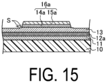
Next, a method for manufacturing the organic EL display device 50 according to the present embodiment will be described. Note that the method for manufacturing the organic EL display device 50 according to the present embodiment includes a TFT layer forming step in which a semiconductor layer forming step, a gate insulating film forming step, a first metal film deposition step, a first photo step, a first etching step a first peeling step, a second metal film deposition step, a second photo step, a second etching step, a second peeling step, and a conductor forming step are sequentially performed, and an organic EL element layer forming step. Here, FIG. 9 is a cross-sectional view illustrating the semiconductor layer forming step in the method for manufacturing the organic EL display device 50, where FIG. 9 is a view corresponding to FIG. 7 . FIG. 10 , FIG. 11 , FIG. 12 , FIG. 13 , FIG. 14 , FIG. 15 , and FIG. 16 are cross-sectional views illustrating the first metal film deposition step, the first photo step, the first etching step, the second metal film deposition step, the second photo step, the second etching step, and the conductor forming step in the method for manufacturing the organic EL display device 50, respectively, and are views corresponding to FIG. 6 .
TFT Layer Forming Step
First, for example, an inorganic insulating film (a thickness of approximately 1000 nm) formed of silicon oxide or the like is formed on the resin substrate layer 10 formed on a glass substrate, for example, by a plasma Chemical Vapor Deposition (CVD) method to form the base coat film 11.
Next, for example, an amorphous silicon film (a thickness of approximately 50 nm) is formed on the entire substrate on which the base coat film 11 is formed, by the plasma CVD method, the amorphous silicon film is crystallized by laser annealing or the like to form a polysilicon film 12 (see the dot-dash line in FIG. 9 ), and subsequently the polysilicon film 12 is patterned to form the semiconductor layer 12 a or the like as illustrated in FIG. 9 (semiconductor layer forming step).
Thereafter, an inorganic insulating film (approximately 100 nm) formed of a silicon oxide film or the like is formed on the entire substrate on which the semiconductor layer 12 a and the like are formed by, for example, the plasma CVD method, to form the gate insulating film 13 to cover the semiconductor layer 12 a (gate insulating film forming step).
Furthermore, a molybdenum film (a thickness of approximately 125 nm) is formed on the entire substrate on which the gate insulating film 13 is formed by, for example, a sputtering method, and the first metal film 14 is formed to cover the gate insulating film 13 as illustrated in FIG. 10 (first metal film deposition step).
Next, the resist R is applied on the first metal film 14, and subsequently, the resist R (dot-dash line in FIG. 11 ) is exposed using the first mask M to form a first resist pattern Ra, as illustrated in FIG. 11 (first photo step).
Then, the first metal film 14 exposed from the first resist pattern Ra is etched to form the first metal layers 14 a, 14 e, 14 g, and the like as illustrated in FIG. 12 (first etching step). Here, in the first etching step, since the surface layer of the gate insulating film 13 underlying the first metal film 14 is also etched, a step having one step is formed on the surface of the gate insulating film 13 as illustrated in FIG. 12 .
Thereafter, the first resist pattern Ra used in the first etching step is peeled (first peeling step).
Furthermore, a molybdenum film (a thickness of approximately 125 nm) is formed by, for example, a sputtering method to peel the first resist pattern Ra to cover the exposed first metal layers 14 a, 14 c, 14 g, and the like and the second metal film 15 is formed as illustrated in FIG. 13 (second metal film deposition step).
Next, the resist R is applied on the second metal film 15, and subsequently, the resist R is exposed using a second mask M to form a second resist pattern Rb, as illustrated in FIG. 14 (second photo step). Here, by making the amount of exposure in the second photo step greater than the amount of exposure in the first photo step, as the second mask M, a mask common to the first mask M can be used.
Furthermore, the second metal film 15 exposed from the second resist pattern Rb is etched to form the second metal layers 15 a, 15 e, 15 g, and the like to form the gate layer including the gate electrode 16 a, the light emission control line 16 e, and the gate line 16 g in which the first metal layer 14 a, 14 e, and 14 g are layered, respectively, as well as the second metal layers 15 a, 15 e, and 15 g, are layered, respectively, as illustrated in FIG. 15 (second etching step). Here, in the second etching step, since the surface layer of the gate insulating film 13 underlying the second metal film 14 is also etched again, a step S having two steps is formed on the surface of the gate insulating film 13 as illustrated in FIG. 15 . Note that it is understood according to the step S having two steps formed on the surface of the gate insulating film 13 that the gate layer including the gate electrode 16 a, the light emission control line 16 e, and the gate line 16 g is formed by repeating the film formation and patterning of the metal film twice.
Thereafter, the second resist pattern Rb used in the second etching step is peeled (second peeling step).
Subsequently, by doping impurity ions into the semiconductor layer 12 a and the like by using the gate electrode 16 a, the light emission control line 16 e, and the gate line 16 g as masks, a portion of the semiconductor layer 12 a and the like is made into electrically conductive to form the semiconductor layers 12 ad, 12 ae, and the like including the conductor region 12 aa, the conductor region 12 ab, and the intrinsic region 12 ac, as illustrated in FIG. 16 (conductor forming step). Note that in the present embodiment, the method for manufacturing in which the conductor forming step is performed after the second peeling step is exemplified, but the conductor forming step may be performed before the second peeling step.
Thereafter, an inorganic insulating film (a thickness of approximately 100 nm) formed of a silicon oxide film or the like is formed on the entire substrate on which the semiconductor layers 12 ad, 12 ae and the like are formed by, for example, the plasma CVD method to form the first interlayer insulating film 17.
Next, a metal film such as a molybdenum film (a thickness of approximately 250 nm) is formed, for example, by a sputtering method on the entire substrate on which the first interlayer insulating film 17 is formed, and subsequently the metal film is patterned to form an intermediate metal layer such as the capacitance electrode 18 c and the initialization power source line 18 i. Note that the intermediate metal layer may be used together with the gate layer as, for example, a lead wiring line for wiring from a terminal of the terminal portion T to the data signal line of the display region D. In this case, in order to have matched wiring line resistance of the lead wiring line, the gate layer and the intermediate metal layer are formed of the same metal material and have the same film thickness preferably. Thus, it is preferable that the intermediate metal layer be a metal layered film of the first metal layer and the second metal layer by a similar step to that of the gate layer.
Furthermore, an inorganic insulating film (a thickness of approximately 500 nm) formed of a silicon oxide film or the like is formed on the entire substrate on which the capacitance electrode 18 c is formed by, for example, the plasma CVD method to form the second interlayer insulating film 19, and subsequently the layered film of the gate insulating film 13, the first interlayer insulating film 17, and the second interlayer insulating film 19 is patterned to form a contact hall.
Thereafter, a titanium film (a thickness of approximately 30 nm), an aluminum film (a thickness of approximately 300 nm), a titanium film (a thickness of approximately 50 nm), and the like are sequentially formed by, for example, a sputtering method on the entire substrate on which the contact hall is formed, to form the source metal film, and subsequently the source metal film is patterned to form the connection wiring line 20 e, the source line 20 f, the power source line 20 g, and the like.
Finally, a polyimide-based photosensitive resin film (a thickness of approximately 2 μm) is applied by, for example, a spin coating method or a slit coating method to the entire substrate on which the connection wiring line 20 e and the like is formed, and subsequently pre-baking, exposing, developing, and post-baking are performed on the applied film to form the flattening film 21.
As described above, the TFT layer 30 a can be formed.
Organic EL Element Layer Forming Step
The first electrode 31, the edge cover 32, the organic EL layer 33 (the hole injection layer 1, the hole transport layer 2, the light-emitting layer 3, the electron transport layer 4, and the electron injection layer 5), and the second electrode 34 are formed on the flattening film 21 of the TFT layer 30 a by using a known method, and subsequently the sealing film 39 (the first sealing inorganic insulating film 36, the sealing organic film 37, and the second sealing inorganic insulating film 38) are formed to form the organic EL element layer 40.
Then, a protective sheet (not illustrated) is bonded on the substrate surface on which the sealing film 39 is formed, and subsequently the laser light is irradiated from the glass substrate side of the resin substrate layer 10, so that the glass substrate is peeled off from a lower surface of the resin substrate layer 10, and subsequently, a protective sheet (not illustrated) is bonded on the lower surface of the resin substrate layer 10 from which the glass substrate has been peeled off.
The organic EL display device 50 of the present embodiment can be manufactured in the manner described above.
Note that in the present embodiment, the organic EL display device 50 including the TFT layer 30 a and the method for manufacturing the same are exemplified, but may be an organic EL display device including a TFT layer 30 b instead of the TFT layer 30 a and the method for manufacturing the same. Here, FIG. 17 and FIG. 18 are a cross-sectional view of the TFT layer 30 b constituting a modified example of the organic EL display device 50 according to the present embodiment, where FIG. 17 and FIG. 18 are views corresponding to FIG. 6 and FIG. 7 .
In the TFT layer 30 a of the present embodiment, the semiconductor layer 12 ad and the like are formed of low-temperature polysilicon. In the TFT layer 30 b of the modified example, however, a semiconductor layer 12 bd and the like are formed of an oxide semiconductor. Thus, in the TFT layer 30 b, only the cross-sectional shape of the underlying gate insulating film 13 b of the semiconductor layer 12 bd of each of the TFTs 9 a to 9 g, and accordingly the cross-sectional shape of the first interlayer insulating film 17 b, the capacitance electrode 18 cb, and the second interlayer insulating film 19 b differ from that of the TFT layer 30 a, and other configurations are substantially the same as those of the TFT layer 30 a.
Describing the drive TFT 9 d representatively, as illustrated in FIG. 17 , the drive TFT 9 d includes a semiconductor layer 12 bd, a gate insulating film 13 b, a gate electrode 16 b, a first interlayer insulating film 17 b, and a second interlayer insulating film 19 b, as well as a first terminal 20 a (see FIG. 3 ) and a second terminal 20 b (see FIG. 3 ), which are sequentially provided on the base coat film 11. Here, similar to the semiconductor layer 12 ad, the semiconductor layer 12 bd is provided in a substantially H-shape on the base coat film 11. Similar to the semiconductor layer 12 ad, the semiconductor layer 12 bd includes an intrinsic region 12 bc provided to overlap with the gate electrode 16 b in a plan view, and a pair of conductor regions 12 ba and 12 bb provided with the intrinsic region 12 bc interposed therebetween. Note that, similar to the intrinsic region 12 ac, the intrinsic region 12 bc is provided with an intermediate portion thereof in a substantially V-shape in a plan view. As illustrated in FIG. 17 and FIG. 18 , the gate insulating film 13 b is provided in an island shape to align with the gate electrode 16 b, the light emission control line 16 e, and the gate line 16 g. As illustrated in FIG. 17 , the gate electrode 16 b is provided in a rectangle island shape in a plan view on the gate insulating film 13 b to overlap with the intrinsic region 12 bc of the semiconductor layer 12 bd. As illustrated in FIG. 17 , the gate electrode 16 b includes a first metal layer 14 b provided on the gate insulating film 13 b, and a second metal layer 15 b provided on the first metal layer 14 b. Note that the first metal layer 14 b and the second metal layer 15 b are formed of the same refractory metal, for example, tungsten, tantalum, molybdenum, niobium, titanium, molybdenum nitride or the like. The intrinsic region 12 bc of the semiconductor layer 12 bd is provided to align with the first metal layer 14 b of the gate electrode 16 b. As illustrated in FIG. 17 and FIG. 18 , the first interlayer insulating film 17 b is provided to cover the gate electrode 16 b, the light emission control line 16 e, and the gate line 16 g. As illustrated in FIG. 17 and FIG. 18 , the second interlayer insulating film 19 b is provided on the first interlayer insulating film 17 b via the capacitance electrode 18 cb.
The organic EL display device including the TFT layer 30 b can be manufactured as will be described below. Here, FIG. 19 , FIG. 20 , and FIG. 21 are cross-sectional views illustrating a second photo step, a second etching step, and a conductor forming step, respectively, in a method for manufacturing the modified example of the organic EL display device according to the present embodiment, where FIG. 19 , FIG. 20 , and FIG. 21 are views corresponding to FIG. 17 .
Furthermore, in the semiconductor layer forming step of the method for manufacturing the organic EL display device 50 described above, an oxide semiconductor film (a thickness of approximately from 30 nm to 100 nm) formed of, for example, InGaZnO4 or the like is formed by a sputtering method on the entire substrate on which the base coat film 11 is formed, and subsequently, a photolithography process, an etching process, and a resist peeling process are performed on the oxide semiconductor film to form the semiconductor layer 12 b (see FIG. 19 ).
Thereafter, the gate insulating film forming step, the first metal film deposition step, the first photo step, the first etching step, the first peeling step, and the second metal film deposition step of the method for manufacturing the organic EL display device 50 described above are sequentially performed, the resist R is applied on the second metal film 15, and subsequently, the resist R is exposed using the second mask M to form a second resist pattern Rbb as illustrated in FIG. 19 (second photo step).
Furthermore, the second metal film 15 exposed from the second resist pattern Rbb, the first metal layer 14 a and the gate insulating film 13 formed in the first etching step are etched to form the gate layer including the gate electrode 16 b and the like in which the first metal layer 14 b and the second metal layer 15 b are layered, and the gate insulating film 13 b as illustrated in FIG. 20 (second etching step).
Thereafter, the second resist pattern Rbb used in the second etching step is peeled (second peeling step).
Subsequently, by performing a plasma treatment such as hydrogen plasma treatment or helium plasma treatment on the semiconductor layer by using the gate electrode 16 b and the like as a mask, a portion of the semiconductor layer is made into electrically conductive to form the semiconductor layer 12 bd including the conductor region 12 ba, the conductor region 12 bb, and the intrinsic region 12 bc as illustrated in FIG. 21 (conductor forming step). Note that in the present modified example, the method for manufacturing in which the conductor forming step is performed after the second peeling step is exemplified, but the conductor forming step may be performed before the second peeling step.
Thereafter, similar to the method for manufacturing the organic EL display device 50 described above, the first interlayer insulating film 17 b, the capacitance electrode 18 cb, the initialization power source line 18 i, the connection wiring line 20 e, the source line 20 f, the power source line 20 g, and the flattening film 21 or the like are formed to form the TFT layer 30 b, and the organic light-emitting element layer forming step described above is performed, so that the organic EL display device including the TFT layer 30 b can be manufactured.
As described above, according to the organic EL display device 50 and the method for manufacturing the same of the present embodiment, the first metal layers 14 a, 14 e, and 14 g formed by the first metal film deposition step, the first photo step, and the first etching step, and the second metal layers 15 a, 15 e and 15 g formed by the second metal film deposition step, the second photo step, and the second etching step are layered on the gate insulating film 13 to form the gate layer including the gate electrode 16 a, the light emission control line 16 e, and the gate line 16 g of the TFT layer 30 a. Here, since the film thickness of the first metal film 14 formed by the first metal film deposition step is half the total film thickness of the first metal film 14 and the second metal film 15, a stress generated in the first metal film 14 can be alleviated as compared with the case where the first metal film 14 and the second metal film 15 are collectively formed. Furthermore, since the film thickness of the second metal film 15 formed by the second metal film deposition step is half the total film thickness of the first metal film 14 and the second metal film 15, a stress generated in the second metal film 15 can be alleviated as compared with the case where the first metal film 14 and the second metal film 15 are collectively formed. As a result, even if the total film thickness of the first metal film 14 and the second metal film 15 is increased in order to reduce the wiring line resistance of the gate layer including the gate electrode 16 a, the light emission control line 16 e, and the gate line 16 g, a stress generated in the first metal film 14 and the second metal film 15 is alleviated, so that the occurrence of cracks in the underlying gate insulating film 13 can be suppressed. Thus, the wiring line resistance of the gate layer including the gate electrode 16 a, the light emission control line 16 e, and the gate line 16 g can be reduced while the occurrence of cracks in the gate insulating film 13 is suppressed.
According to the organic EL display device 50 and the method for manufacturing the same of the present embodiment, since residues of the first metal film 14 remaining in the first etching step can be removed in the second etching step, for example, inter-wiring line leaks between the gate electrode 16 a and the gate line 16 g and between the gate electrode 16 a and the light emission control line 16 e having narrow intervals can be suppressed.
Second Embodiment
FIG. 22 to FIG. 28 illustrate a second embodiment of the display device and the method for manufacturing the same according to the disclosure. Here, FIG. 22 is a plan view of a TFT layer 30 c included in an organic EL display device according to the present embodiment. FIG. 23 is a cross-sectional view of the TFT layer 30 c taken along a line XXIII-XXIII in FIG. 22 . Note that, in each of the following embodiments, the same portions as those in FIG. 1 to FIG. 21 are denoted by the same reference signs, and detailed description of these portions are omitted.
In the first embodiment described above, the organic EL display device 50 and the method for manufacturing the same, in which the conductor forming step is performed after the second etching step, are exemplified, but in the present embodiment, an organic EL display device and a method for manufacturing the same in which a conductor forming step is performed prior to the second metal film deposition step is exemplified.
Similar to the organic EL display device 50 of the first embodiment described above, the organic EL display device of the present embodiment includes the display region D and the frame region F provided on the periphery of the display region D. Similar to the organic EL display device 50 of the first embodiment described above, the organic EL display device of the present embodiment includes the resin substrate layer 10, the TFT layer 30 c provided on the resin substrate layer 10, and the organic EL element layer 40 provided on the TFT layer 30 c.
Similar to the TFT layer 30 a of the organic EL display device 50 of the first embodiment described above, the TFT layer 30 c includes the base coat film 11 provided on the resin substrate layer 10, the first initialization TFT 9 a, the threshold voltage compensation TFT 9 b, the write control TFT 9 c, the drive TFT 9 d, the power source supply TFT 9 e, the light emission control TFT 9 f, the second initialization TFT 9 g, and the capacitor 9 h provided for each subpixel P on the base coat film 11, and the flattening film 21 provided on each of the TFTs 9 a to 9 g and the capacitor 9 h.
As illustrated in FIG. 23 , the drive TFT 9 d includes a semiconductor layer 12 cd, the gate insulating film 13, the gate electrode 16 c, the first interlayer insulating film 17, and the second interlayer insulating film 19, as well as the first terminal 20 a (see FIG. 3 ) and the second terminal 20 b (see FIG. 3 ), which are sequentially provided on the base coat film 11. Here, the semiconductor layer 12 cd is formed of low-temperature polysilicon and is provided in a substantially H-shape on the base coat film 11, as illustrated in FIG. 22 and FIG. 23 . As illustrated in FIG. 23 , the semiconductor layer 12 cd includes an intrinsic region 12 cc provided to overlap with the gate electrode 16 c in a plan view, and a pair of conductor regions 12 ca and 12 cb provided with an intrinsic region 12 cc interposed therebetween. Note that, as illustrated in FIG. 22 , the intrinsic region 12 cc is provided with an intermediate portion thereof in a substantially V-shape in a plan view. As illustrated in FIG. 22 and FIG. 23 , offset regions Y are provided in respective portions of the intrinsic region 12 cc, the portions being on the respective sides with the pair of conductor regions 12 ca and 12 cb so as not to overlap with the first metal layer 14 c and the second metal layer 15 c described later. As illustrated in FIG. 23 , the gate insulating film 13 is provided to cover the semiconductor layer 12 cd. Note that, a step S having two steps along the circumferential end of the gate electrode 16 c formed by first and second etching steps resides on the surface of the gate insulating film 13 exposed from the gate electrode 16 a. The boundaries between the pair of conductor regions 12 ca and 12 cb and the intrinsic region 12 cc are provided to align with the step S formed on the surface of the gate insulating film 13. As illustrated in 22, and 23, the gate electrode 16 c is provided in a rectangle island shape in a plan view on the gate insulating film 13 to overlap with the intrinsic region 12 cc of the semiconductor layer 12 cd. As illustrated in FIG. 23 , the gate electrode 16 c includes a first metal layer 14 c provided on the gate insulating film 13, and a second metal layer 15 c provided on the first metal layer 14 c. Note that as illustrated in FIG. 22 and FIG. 23 , in a direction L (the horizontal direction in FIG. 22 ) of the channel length of the intrinsic region 12 cc of the semiconductor layer 12 cd and in a direction orthogonal thereto (the vertical direction in FIG. 22 ), the length of the second metal layer 15 c is equal to or less than the length of the first metal layer 14 c. The first metal layer 14 c and the second metal layer 15 c are formed of the same refractory metal, for example, tungsten, tantalum, molybdenum, niobium, titanium, molybdenum nitride, or the like. The intrinsic region 12 cc of the semiconductor layer 12 cd is provided to align with the first metal layer 14 a serving as the first metal layer 14 c. As illustrated in FIG. 23 , the first interlayer insulating film 17 is provided to cover the gate electrode 16 c, the light emission control line 16 e, and the gate line 16 g. As illustrated in FIG. 23 , the second interlayer insulating film 19 is provided on the first interlayer insulating film 17 via the capacitance electrode 18 c. The first terminal 20 a and the second terminal 20 b are electrically connected to the pair of the conductor regions 12 ca and 12 cb of the semiconductor layer 12 cd via respective contact holes formed in a layered film of the gate insulating film 13, the first interlayer insulating film 17, and the second interlayer insulating film 19.
Note that the first initialization TFT 9 a, the threshold voltage compensation TFT 9 b, the write control TFT 9 c, the power source supply TFT 9 e, the light emission control TFT 9 f, and the second initialization TFT 9 g have similar configurations to that of the drive TFT 9 d described above except that the capacitance electrode 18 c is not interposed.
Similar to the organic EL display device 50 of the first embodiment described above, the organic EL display device including the TFT layer 30 c having above-described configuration has flexibility and is configured to display an image by causing the light-emitting layer 3 of the organic EL layer 33 to emit light as appropriate via the first initialization TFT 9 a, the threshold voltage compensation TFT 9 b, the write control TFT 9 c, the drive TFT 9 d, the power source supply TFT 9 e, the light emission control TFT 9 f, and the second initialization TFT 9 g in each subpixel P.
Next, a method for manufacturing the organic EL display device including the TFT layer 30 c according to the present embodiment will be described. Note that the method for manufacturing the organic EL display device according to the present embodiment includes a TFT layer forming step in which a semiconductor layer forming step, a gate insulating film forming step, a first metal film deposition step, a first photo step, a first etching step, a first peeling step, a conductor forming step, a second metal film deposition step, a second photo step, a second etching step, and a second peeling step are sequentially performed, and an organic EL element layer forming step. Here, FIG. 24 , FIG. 25 , FIG. 26 , and FIG. 27 are cross-sectional views illustrating the conductor forming step, the second metal film deposition step, the second photo step, and the second etching step, respectively, in the method for manufacturing the organic EL display device according to the present embodiment, where FIG. 24 , FIG. 25 , FIG. 26 , and FIG. 27 are views corresponding to FIG. 23 .
First, up to the first peeling step of the method for manufacturing the organic EL display device 50 described in the first embodiment above is performed, and subsequently by doping impurity ions into the semiconductor layer 12 a and the like by using the first metal layer 14 a as a mask, a portion of the semiconductor layer 12 a and the like is made into electrically conductive to form the semiconductor layer 12 cd including the conductor region 12 ca, the conductor region 12 cb, and the intrinsic region 12 cc as illustrated in FIG. 24 (conductor forming step). Note that in the present embodiment, the method for manufacturing in which the conductor forming step is performed after the first peeling step is exemplified, but the conductor forming step may be performed before the first peeling step.
Next, a molybdenum film (a thickness of approximately 125 nm) is formed by, for example, a sputtering method to cover the first metal layer 14 a and the like and the second metal film 15 is formed, as illustrated in FIG. 25 (second metal film deposition step).
Thereafter, the resist R is applied on the second metal film 15, and subsequently, the resist R (dot-dash line in FIG. 26 ) is exposed using the second mask M to form the second resist pattern Rbc, as illustrated in FIG. 26 (second photo step). Here, by making the amount of exposure in the second photo step greater than the amount of exposure in the first photo step, as the second mask M, a mask common to the first mask M can be used. Note that in the direction L of the channel length of the semiconductor layer 12 cd, the length of the second resist pattern Rbc is shorter than the length of the first resist pattern Ra.
Furthermore, the second metal film 15 exposed from the second resist pattern Rbc is etched to form the second metal layer 15 c and the like, to form the gate layer including the gate electrode 16 c in which the first metal layer 14 c and the second metal layer 15 c are layered, as illustrated in FIG. 27 (second etching step). Here, in the second etching step, since the surface layer of the gate insulating film 13 underlying the second metal film 14 is also etched again, the step S having two steps is formed on the surface of the gate insulating film 13 as illustrated in FIG. 27 .
Thereafter, the second resist pattern Rbc used in the second etching step is peeled (second peeling step), and subsequently, similar to the first embodiment described above, the first interlayer insulating film 17, the capacitance electrode 18 c, the initialization power source line 18 i, the connection wiring line 20 e, the source line 20 f, the power source line 20 g, the flattening film 21, and the like are formed to form the TFT layer 30 c, and subsequently the organic EL element layer forming step is performed, so that the organic EL display device including the TFT layer 30 c can be manufactured.
Note that in the present embodiment, the organic EL display device including the TFT layer 30 c and the method for manufacturing the same are exemplified, but may alternatively be an organic EL display device including a TFT layer 30 d instead of the TFT layer 30 c and a method for manufacturing the same. Here, FIG. 28 is a cross-sectional view of the TFT layer 30 d constituting a modified example of the organic EL display device according to the present embodiment, where FIG. 28 is a view corresponding to FIG. 23 .
In the TFT layer 30 c of the present embodiment, the semiconductor layer 12 cd and the like are formed of low-temperature polysilicon. In the TFT layer 30 d of the modified example, however, a semiconductor layer 12 dd and the like are formed of an oxide semiconductor. Thus, in the TFT layer 30 d, only the cross-sectional shape of an underlying gate insulating film 13 d of the semiconductor layer 12 dd of each of the TFTs 9 a to 9 g, and accordingly the cross-sectional shape of the first interlayer insulating film 17 b, the capacitance electrode 18 cb, and the second interlayer insulating film 19 b differ from that of the TFT layer 30 c, and other configurations are substantially the same as those of the TFT layer 30 c.
Describing the drive TFT 9 d representatively, as illustrated in FIG. 28 , the drive TFT 9 d includes the semiconductor layer 12 dd, the gate insulating film 13 d, a gate electrode 16 d, the first interlayer insulating film 17 b, and the second interlayer insulating film 19 b, as well as the first terminal 20 a (see FIG. 3 ) and the second terminal 20 b (see FIG. 3 ), which are sequentially provided on the base coat film 11. Here, similar to the semiconductor layer 12 cd, the semiconductor layer 12 dd is provided in a substantially H-shape on the base coat film 11. Similar to the semiconductor layer 12 cd, as illustrated in FIG. 28 , the semiconductor layer 12 dd includes an intrinsic region 12 dc provided to overlap with the gate electrode 16 b in a plan view, and a pair of conductor regions 12 da and 12 db provided with the intrinsic region 12 dc interposed therebetween. Note that, similar to the intrinsic region 12 cc, the intrinsic region 12 dc is provided with an intermediate portion thereof in a substantially V-shape in a plan view. As illustrated in FIG. 28 , offset regions Y are provided in respective portions of the intrinsic region 12 dc, the portions being on respective sides with the pair of conductor regions 12 da and 12 db so as not to overlap with a first metal layer 14 d and a second metal layer 15 d described later. As illustrated in FIG. 28 , the gate insulating film 13 d is provided in an island shape to align with the gate electrode 16 d, the light emission control line 16 e, and the gate line 16 g. The boundaries between the pair of conductor regions 12 da and 12 db and the intrinsic region 12 dc are provided to align with the end portions of the gate insulating film 13 d. As illustrated in FIG. 28 , the gate electrode 16 d is provided in a rectangle island shape in a plan view on the gate insulating film 13 to overlap with the intrinsic region 12 dc of the semiconductor layer 12 dd. As illustrated in FIG. 28 , the gate electrode 16 d includes the first metal layer 14 d provided on the gate insulating film 13 d, and a second metal layer 15 d provided on the first metal layer 14 d. Note that the first metal layer 14 d and the second metal layer 15 d are formed of the same refractory metal, for example, tungsten, tantalum, molybdenum, niobium, titanium, molybdenum nitride, or the like. As illustrated in FIG. 28 , the first interlayer insulating film 17 b is provided to cover the gate electrode 16 d, the light emission control line 16 e, and the gate line 16 g. As illustrated in FIG. 28 , the second interlayer insulating film 19 b is provided on the first interlayer insulating film 17 b via the capacitance electrode 18 cb.
The organic EL display device including the TFT layer 30 d described above can be manufactured by combining the method for manufacturing of the present embodiment and the method for manufacturing of the above-described modified example of the first embodiment.
As described above, according to the organic EL display device and the method for manufacturing the same of the present embodiment, the first metal layer 14 a formed by the first metal film deposition step, the first photo step, and the first etching step, and the second metal layer 15 a formed by the second metal film deposition step, the second photo step, and the second etching step are layered on the gate insulating film 13 to form a gate layer including the gate electrode 16 c of the TFT layer 30 c. Here, since the film thickness of the first metal film 14 formed by the first metal film deposition step is half the total film thickness of the first metal film 14 and the second metal film 15, a stress generated in the first metal film 14 can be alleviated as compared with the case where the first metal film 14 and the second metal film 15 are collectively formed. Furthermore, since the film thickness of the second metal film 15 formed by the second metal film deposition step is half the total film thickness of the first metal film 14 and the second metal film 15, a stress generated in the second metal film 15 can be alleviated as compared with the case where the first metal film 14 and the second metal film 15 are collectively formed. As a result, even if the total film thickness of the first metal film 14 and the second metal film 15 is increased in order to reduce the wiring line resistance of the gate layer including the gate electrode 16 c, the stress generated in the first metal film 14 and the second metal film 15 is alleviated, so that the occurrence of cracks in the underlying gate insulating film 13 can be suppressed. Thus, the wiring line resistance of the gate layer including the gate electrode 16 c can be reduced while the occurrence of cracks in the gate insulating film 13 is suppressed.
According to the organic EL display device and the method for manufacturing the same of the present embodiment, since residues of the first metal film 14 remaining in the first etching step can be removed in the second etching step, for example, inter-wiring line leaks between the gate electrode 16 c and the gate line 16 g and between the gate electrode 16 c and the light emission control line 16 e having narrow intervals can be suppressed.
According to the organic EL display device and the method for manufacturing the same of the present embodiment, since the organic EL display device of the present embodiment includes the TFTs 9 a to 9 g having the offset regions Y, an S value (a rising coefficient in a subthreshold region) of the TFTs 9 a to 9 g can be increased, and a leakage current can be reduced.
Third Embodiment
FIG. 29 to FIG. 32 illustrate a third embodiment of the display device and the method for manufacturing the same according to the disclosure. Here, FIG. 29 is a plan view of a TFT layer 30 e included in an organic EL display device according to the third embodiment of the disclosure. FIG. 30 is a cross-sectional view of the TFT layer 30 e taken along a line XXX-XXX in FIG. 29 .
In the first and second embodiments, the organic EL display device including any of the TFT layers 30 a to 30 d provided such that the side surface of the second metal layer and the side surface of the first metal layer align with each other in the gate electrodes of the TFTs is exemplified. In the present embodiment, however, an organic EL display device including the TFT layer 30 e provided such that a portion of a second metal layer 15 ae protrudes from an end portion of a first metal layer 14 ae in the gate electrode of the TFT is exemplified.
Similar to the organic EL display device 50 of the first embodiment described above, the organic EL display device of the present embodiment includes the display region D and the frame region F provided on the periphery of the display region D. Similar to the organic EL display device 50 of the first embodiment described above, the organic EL display device of the present embodiment includes the resin substrate layer 10, the TFT layer 30 e provided on the resin substrate layer 10, and the organic EL element layer 40 provided on the TFT layer 30 e.
Similar to the TFT layer 30 a of the organic EL display device 50 of the first embodiment described above, the TFT layer 30 e includes the base coat film 11 provided on the resin substrate layer 10, the first initialization TFT 9 a, the threshold voltage compensation TFT 9 b, the write control TFT 9 c, the drive TFT 9 d, the power source supply TFT 9 e, the light emission control TFT 9 f, the second initialization TFT 9 g, and the capacitor 9 h provided for each subpixel P on the base coat film 11, and the flattening film 21 provided on each of the TFTs 9 a to 9 g and the capacitor 9 h.
As illustrated in FIG. 30 , the drive TFT 9 d includes the semiconductor layer 12 cd, the gate insulating film 13, a gate electrode 16 ae, a first interlayer insulating film 17 e, a second interlayer insulating film 19 e, as well as the first terminal 20 a (see FIG. 3 ) and the second terminal 20 b (see FIG. 3 ), which are sequentially provided on the base coat film 11. Here, the semiconductor layer 12 cd is formed of low-temperature polysilicon and is provided in a substantially H-shape on the base coat film 11, as illustrated in FIG. 29 and FIG. 30 . As illustrated in FIG. 30 , the semiconductor layer 12 cd includes the intrinsic region 12 cc provided to overlap with the gate electrode 16 ae in a plan view, and the pair of conductor regions 12 ca and 12 cb provided with the intrinsic region 12 cc interposed therebetween. Note that, as illustrated in FIG. 29 , the intrinsic region 12 cc is provided with an intermediate portion thereof in a substantially V-shape in a plan view. As illustrated in FIG. 30 , the gate insulating film 13 is provided to cover the semiconductor layer 12 cd. Note that the boundaries between the pair of conductor regions 12 ca and 12 cb and the intrinsic region 12 cc are provided to align with the end portions of the first metal layer 14 ae of the gate electrode 16 ae as illustrated in FIG. 30 . As illustrated in FIG. 29 and FIG. 31 , the gate electrode 16 ae is provided in a rectangle island shape in a plan view on the gate insulating film 13 to overlap with the intrinsic region 12 cc of the semiconductor layer 12 cd. As illustrated in FIG. 30 , the gate electrode 16 ae includes the first metal layer 14 ae provided on the gate insulating film 13, and the second metal layer 15 ae provided on the first metal layer 14 ae. Note that, in the portion of the gate electrode 16 ae overlapping with the intrinsic region 12 cc, the second metal layer 15 ae is provided to protrude from both end portions of the first metal layer 14 ae to cover the first metal layer 14 ae in a direction L of the channel length of the semiconductor layer 12 cd, as illustrated in FIG. 29 and FIG. 30 . A portion A of the gate electrode 16 ae that does not overlap with the semiconductor layer 12 cd is provided such that the width of the second metal layer 15 ae is equal to or less than the width of the first metal layer 14 ae, as illustrated in FIG. 29 . The portion A of the light emission control line 16 ee that does not overlap with the semiconductor layer 12 cd is provided such that the width of the second metal layer 15 ee is equal to or less than the width of the first metal layer 14 e, as illustrated in FIG. 29 . The portion A of a gate line 16 ge that does not overlap with the semiconductor layer 12 cd is provided such that the width of a second metal layer 15 ge is equal to or less than the width of the first metal layer 14 g, as illustrated in FIG. 29 . The first metal layer 14 ae and the second metal layer 15 ae are formed of the same refractory metal, for example, tungsten, tantalum, molybdenum, niobium, titanium, molybdenum nitride, or the like. The intrinsic region 12 cc of the semiconductor layer 12 cd is provided to align with the first metal layer 14 ae. As illustrated in FIG. 30 , the first interlayer insulating film 17 e is provided to cover the gate electrode 16 ae, the light emission control line 16 ee, and the gate line 16 ge. As illustrated in FIG. 30 , the second interlayer insulating film 19 e is provided on the first interlayer insulating film 17 e via the capacitance electrode 18 c. The first terminal 20 a and the second terminal 20 b are electrically connected to the pair of the conductor regions 12 ca and 12 cb of the semiconductor layer 12 cd, respectively, via respective contact holes formed in a layered film of the gate insulating film 13, the first interlayer insulating film 17 e, and the second interlayer insulating film 19 e.
Note that the first initialization TFT 9 a, the threshold voltage compensation TFT 9 b, the write control TFT 9 c, the power source supply TFT 9 e, the light emission control TFT 9 f, and the second initialization TFT 9 g have similar configurations to that of the drive TFT 9 d described above except that the capacitance electrode 18 c is not interposed.
Similar to the organic EL display device 50 of the first embodiment described above, the organic EL display device including the TFT layer 30 e having above-describe configuration has flexibility and is configured to display an image by causing the light-emitting layer 3 of the organic EL layer 33 to emit light as appropriate via the first initialization TFT 9 a, the threshold voltage compensation TFT 9 b, the write control TFT 9 c, the drive TFT 9 d, the power source supply TFT 9 e, the light emission control TFT 9 f, and the second initialization TFT 9 g in each subpixel P.
Next, a method for manufacturing the organic EL display device including the TFT layer 30 e according to the present embodiment will be described. Note that the method for manufacturing the organic EL display device according to the present embodiment includes a TFT layer forming step in which a semiconductor layer forming step, a gate insulating film forming step, a first metal film deposition step, a first photo step, a first etching step, a first peeling step, a conductor forming step, a second metal film deposition step, a second photo step, a second etching step, and a second peeling step are sequentially performed, and an organic EL element layer forming step. Here, FIG. 31 and FIG. 32 are cross-sectional views illustrating the second photo step and the second etching step, respectively, in the method for manufacturing the organic EL display device according to the present embodiment, where FIG. 31 and FIG. 32 are views corresponding to FIG. 30 .
First, up to the first peeling step of the method for manufacturing the organic EL display device 50 described in the first embodiment above is performed, and subsequently by doping impurity ions into the semiconductor layer 12 a and the like by using the first metal layer 14 a as a mask, a portion of the semiconductor layer 12 a and the like is made into electrically conductive to form the semiconductor layer 12 cd including the conductor region 12 ca, the conductor region 12 cb, and the intrinsic region 12 cc as illustrated in FIG. 24 (conductor forming step). Note that in the present embodiment, the method for manufacturing in which the conductor forming step is performed after the first peeling step is exemplified, but the conductor forming step may be performed before the first peeling step.
Next, a molybdenum film (a thickness of approximately 125 nm) is formed by, for example, a sputtering method to cover the first metal layer 14 a and the like to form the second metal film 15, as illustrated in FIG. 25 (second metal film deposition step).
Thereafter, the resist R (dot-dash line in FIG. 31 ) is applied on the second metal film 15, and subsequently, the resist R is exposed using the second mask M to form a second resist pattern Rbe, as illustrated in FIG. 31 (second photo step). Here, in the second photo step, the second resist pattern Rbe is formed to protrude from both end portions of the first metal layer 14 a in a direction L of the channel length of the semiconductor layer 12 cd.
Furthermore, the second metal film 15 exposed from the second resist pattern Rbe is etched to form the second metal layers 15 ae, 15 ee, 15 gef, and the like, as illustrated in FIG. 32 , and to form the gate layer including the gate electrode 16 ae, the light emission control line 16 ee, and the gate line 16 ge in which the first metal layer 14 a, 14 e, and 14 g and the second metal layers 15 ae, 15 ee, and 15 ge are layered, respectively (second etching step). Here, in the second etching step, the second metal layer 15 ae is formed to cover the both end portions of the first metal layer 14 ae and between the both end portions in the direction L of the channel length of the semiconductor layer 12 cd. In the second etching step, since the surface layer of the gate insulating film 13 underlying the second metal film 14 is also etched again, the step S having two steps is formed on the surface of the gate insulating film 13 as illustrated in FIG. 32 .
Thereafter, the second resist pattern Rbe used in the second etching step is peeled (second peeling step), and subsequently similar to the first embodiment described above, the first interlayer insulating film 17, the capacitance electrode 18 c, the initialization power source line 18 i, the connection wiring line 20 e, the source line 20 f, the power source line 20 g, and the flattening film 21 and the like are formed to form the TFT layer 30 e, and subsequently the organic EL element layer forming step is performed, so that the organic EL display device including the TFT layer 30 e can be manufactured.
As described above, according to the organic EL display device and the method for manufacturing the same of the present embodiment, the first metal layer 14 ae formed by the first metal film deposition step, the first photo step, and the first etching step, and the second metal layer 15 ae formed by the second metal film deposition step, the second photo step, and the second etching step are layered on the gate insulating film 13 to form the gate layer including the gate electrode 16 ae of the TFT layer 30 e. Here, since the film thickness of the first metal film 14 formed by the first metal film deposition step is half the total film thickness of the first metal film 14 and the second metal film 15, a stress generated in the first metal film 14 can be alleviated as compared with the case where the first metal film 14 and the second metal film 15 are collectively formed. Furthermore, since the film thickness of the second metal film 15 formed by the second metal film deposition step is half the total film thickness of the first metal film 14 and the second metal film 15, a stress generated in the second metal film 15 can be alleviated as compared with the case where the first metal film 14 and the second metal film 15 are collectively formed. As a result, even if the total film thickness of the first metal film 14 and the second metal film 15 is increased in order to reduce the wiring line resistance of the gate layer including the gate electrode 16 ae, the stress generated in the first metal film 14 and the second metal film 15 is alleviated, so that the occurrence of cracks in the underlying gate insulating film 13 can be suppressed. Thus, the wiring line resistance of the gate layer including the gate electrode 16 ae can be reduced while the occurrence of cracks in the gate insulating film 13 is suppressed.
According to the organic EL display device and the method for manufacturing the same of the present embodiment, since residues of the first metal film 14 remaining in the first etching step can be removed in the second etching step, for example, inter-wiring line leaks between the gate electrode 16 ae and the gate line 16 ge and between the gate electrode 16 ae and the light emission control line 16 ee having narrow intervals can be suppressed.
According to the organic EL display device and the method for manufacturing the same of the present embodiment, the boundaries between the pair of conductor regions 12 ca and 12 cb and the intrinsic region 12 cc are provided to align with the end portions of the first metal layer 14 a of the gate electrode 16 ae, and the second metal layer 15 ae of the gate electrode 16 ae is provided to protrude from the both end portions of the first metal layer 14 a to cover the first metal layer 14 a in the direction L of the channel length of the semiconductor layer 12 cd, so that the TFTs 9 a to 9 g having no offset region Y can be formed.
Note that in the present embodiment, the configuration in which the semiconductor layer is formed of low-temperature polysilicon is exemplified, but the present invention is also applicable to the case where the semiconductor layer is formed of the oxide semiconductor layer. In this case, the gate insulating film does not align with the end portions of the gate electrode, and is provided entirely on the base coat layer or the semiconductor layer except for contact holes and the like, as is the case where the semiconductor layer is formed of low-temperature polysilicon. Here, the conductor forming process is performed via the gate insulating film. Furthermore, the shapes of the step formed in the gate insulating film, and the intrinsic region and the conductor region of the semiconductor layer are similar to those in the case where the semiconductor layer is formed of the low-temperature polysilicon.
Fourth Embodiment
FIG. 33 illustrates a fourth embodiment of the display device and the method for manufacturing the same according to the disclosure. Here, FIG. 33 is a plan view of a TFT layer 30 f included in an organic EL display device of the present embodiment.
The above-described second embodiment exemplifies the organic EL display device including the TFT layer 30 c provided with TFTs 9 a to 9 g having the offset region Y, and the above-described third embodiment exemplifies the organic EL display device including the TFT layer 30 e provided with the TFTs 9 a to 9 g having no offset regions Y. The present embodiment exemplifies an organic EL display device including the TFT layer 30 f combining the TFTs 9 a, 9 b, and 9 d having the offset regions Y and the TFTs 9 c, 9 e, 9 f, and 9 g having no offset region Y.
Specifically, in a case where a TFT having the offset region Y is defined as a first TFT and a TFT having no offset region Y is defined as a second TFT, the organic EL display device may include the TFT layer 30 f provided with the first initialization TFT 9 a (not illustrated), the threshold voltage compensation TFT 9 b, and the drive TFT 9 d as the first TFTs, and provided with the write control TFT 9 c, the power source supply TFT 9 e, the light emission control TFT 9 f, and the second initialization TFT 9 g (not illustrated) as the second TFTs, as illustrated in FIG. 33 .
Here, in the first TFTs (9 a, 9 b, and 9 d) including the first semiconductor layer including the first intrinsic region and the pair of first conductor regions and the first gate layer, as illustrated in FIG. 23 , the offset regions Y are provided in respective portions of the first intrinsic region 12 cc, the portions being respective sides with the pair of first conductor regions 12 ca and 12 cb, so as not to overlap with the first metal layer 14 a and the second metal layer 15 a, boundaries between the pair of first conductor regions 12 ca and 12 cb and the first intrinsic region 12 cc are provided to align with the step S formed on the surface of the gate insulating film 13, and the length of the second metal layer 15 a is equal to or less than the length of the first metal layer 14 a in the direction L of a channel length of the first semiconductor layer 12 cd.
In the second TFTs (9 c, 9 e, 9 f, and 9 g) including the second semiconductor layer including the second intrinsic region and the pair of second conductor regions and the second gate layer, as illustrated in FIG. 33 (see FIG. 30 ), boundaries between the pair of second conductor regions 12 ca and 12 cb and the second intrinsic region 12 cc are provided to align with the end portions of the first metal layers 14 e and 14 g, and in the second gate layer (the light emission control line 16 ee and the gate line 16 gf) overlapping with the second intrinsic region 12 cc, the second metal layers 15 ee and 15 gf are provided to protrude from both end portions of the first metal layers 14 e and 14 g to cover the first metal layers 14 e and 14 g, in the direction L of the channel length of the second semiconductor layer 12 cd. The portion of the second gate layer (the light emission control line 16 ee and the gate line 16 gf) that does not overlap with the second intrinsic region 12 cc is provided such that the width of the second metal layers 15 ee and 15 gf is equal to or less than the width of the first metal layers 14 e and 14 g, as illustrated in FIG. 33 .
Note that in the present embodiment, the configuration in which the semiconductor layer is formed of the low-temperature polysilicon is exemplified. The semiconductor layer, however, may be formed of the oxide semiconductor layer.
Other Embodiments
In each of the embodiments described above, the organic EL layer having a five-layered structure including the hole injection layer, the hole transport layer, the light-emitting layer, the electron transport layer, and the electron injection layer is exemplified, but the organic EL layer may have a three-layered structure including a hole injection-cum-transport layer, a light-emitting layer, and an electron transport-cum-injection layer, for example.
In each of the embodiments described above, the organic EL display device including the first electrode as an anode and the second electrode as a cathode is exemplified. The disclosure is also applicable to an organic EL display device in which the layered structure of the organic EL layer is reversed with the first electrode being a cathode and the second electrode being an anode.
In each of the embodiments described above, the organic EL display device including a top gate type TFT is exemplified, but the disclosure is also applicable to an organic EL display device including a bottom gate type TFT.
In each of the embodiments described above, the organic EL display device 50 including the sealing film 39 provided with the sealing organic film 37 between the first sealing inorganic insulating film 36 and the second sealing inorganic insulating film 38 is exemplified. The disclosure is also applicable to an organic EL display device in which an organic vapor deposition film is formed between the first sealing inorganic insulating film 36 and the second sealing inorganic insulating film 38, and subsequently the organic vapor deposition film is ashed to cover the foreign matters with the organic vapor deposition film. According to such a configuration of the sealing film, even if the foreign matters are present on the display region, the sealing performance can be ensured by the second sealing inorganic insulating film, and the reliability can be improved.
In addition, in each of the embodiments described above, the organic EL display device is exemplified and described as the display device. The disclosure is, however, not limited to the organic EL display device and also applicable to any flexible display device. For example, the disclosure is applicable to a flexible display device including QLEDs or the like that are light-emitting elements using a quantum dot containing layer.
INDUSTRIAL APPLICABILITY
As described above, the disclosure is useful for a flexible display device.