US12081226B2 - Feed-forward in tracking analog-to-digital converter - Google Patents
Feed-forward in tracking analog-to-digital converter Download PDFInfo
- Publication number
- US12081226B2 US12081226B2 US17/931,065 US202217931065A US12081226B2 US 12081226 B2 US12081226 B2 US 12081226B2 US 202217931065 A US202217931065 A US 202217931065A US 12081226 B2 US12081226 B2 US 12081226B2
- Authority
- US
- United States
- Prior art keywords
- circuit
- feedback
- signal
- voltage
- comparison
- Prior art date
- Legal status (The legal status is an assumption and is not a legal conclusion. Google has not performed a legal analysis and makes no representation as to the accuracy of the status listed.)
- Active, expires
Links
- 230000004044 response Effects 0.000 claims description 53
- 238000000034 method Methods 0.000 claims description 37
- 230000004913 activation Effects 0.000 claims description 10
- 230000009849 deactivation Effects 0.000 claims description 9
- 238000012544 monitoring process Methods 0.000 claims description 9
- 230000003213 activating effect Effects 0.000 claims description 6
- 230000002401 inhibitory effect Effects 0.000 claims description 2
- 238000005070 sampling Methods 0.000 claims description 2
- 230000002829 reductive effect Effects 0.000 abstract description 2
- 230000008901 benefit Effects 0.000 description 16
- 238000010586 diagram Methods 0.000 description 16
- 230000006870 function Effects 0.000 description 15
- 230000015654 memory Effects 0.000 description 14
- 230000004048 modification Effects 0.000 description 14
- 238000012986 modification Methods 0.000 description 14
- 230000002093 peripheral effect Effects 0.000 description 7
- 238000013461 design Methods 0.000 description 6
- 230000036541 health Effects 0.000 description 6
- 230000001419 dependent effect Effects 0.000 description 4
- 238000005516 engineering process Methods 0.000 description 4
- 238000012545 processing Methods 0.000 description 4
- 230000008859 change Effects 0.000 description 3
- 238000006243 chemical reaction Methods 0.000 description 3
- 238000004891 communication Methods 0.000 description 3
- 230000000694 effects Effects 0.000 description 3
- 238000004519 manufacturing process Methods 0.000 description 3
- 238000012806 monitoring device Methods 0.000 description 3
- 230000007704 transition Effects 0.000 description 3
- OKTJSMMVPCPJKN-UHFFFAOYSA-N Carbon Chemical compound [C] OKTJSMMVPCPJKN-UHFFFAOYSA-N 0.000 description 2
- 230000003542 behavioural effect Effects 0.000 description 2
- 230000001413 cellular effect Effects 0.000 description 2
- 238000001816 cooling Methods 0.000 description 2
- 238000011156 evaluation Methods 0.000 description 2
- 230000000670 limiting effect Effects 0.000 description 2
- 230000008569 process Effects 0.000 description 2
- 230000009467 reduction Effects 0.000 description 2
- JBRZTFJDHDCESZ-UHFFFAOYSA-N AsGa Chemical compound [As]#[Ga] JBRZTFJDHDCESZ-UHFFFAOYSA-N 0.000 description 1
- 229910001218 Gallium arsenide Inorganic materials 0.000 description 1
- 230000003466 anti-cipated effect Effects 0.000 description 1
- 238000003491 array Methods 0.000 description 1
- 230000003190 augmentative effect Effects 0.000 description 1
- 239000003990 capacitor Substances 0.000 description 1
- 239000002041 carbon nanotube Substances 0.000 description 1
- 229910021393 carbon nanotube Inorganic materials 0.000 description 1
- 238000001514 detection method Methods 0.000 description 1
- 230000009977 dual effect Effects 0.000 description 1
- 230000007613 environmental effect Effects 0.000 description 1
- 239000004744 fabric Substances 0.000 description 1
- 238000009472 formulation Methods 0.000 description 1
- 239000011521 glass Substances 0.000 description 1
- 229910021389 graphene Inorganic materials 0.000 description 1
- 238000010438 heat treatment Methods 0.000 description 1
- 230000006872 improvement Effects 0.000 description 1
- 230000007246 mechanism Effects 0.000 description 1
- 239000000203 mixture Substances 0.000 description 1
- 230000003071 parasitic effect Effects 0.000 description 1
- 230000008439 repair process Effects 0.000 description 1
- 230000000630 rising effect Effects 0.000 description 1
- 239000007787 solid Substances 0.000 description 1
- 230000005236 sound signal Effects 0.000 description 1
- 230000003068 static effect Effects 0.000 description 1
- 230000001360 synchronised effect Effects 0.000 description 1
- 230000002123 temporal effect Effects 0.000 description 1
- 238000012546 transfer Methods 0.000 description 1
- 230000001960 triggered effect Effects 0.000 description 1
Images


Classifications
-
- H—ELECTRICITY
- H03—ELECTRONIC CIRCUITRY
- H03M—CODING; DECODING; CODE CONVERSION IN GENERAL
- H03M1/00—Analogue/digital conversion; Digital/analogue conversion
- H03M1/12—Analogue/digital converters
- H03M1/48—Servo-type converters
-
- H—ELECTRICITY
- H03—ELECTRONIC CIRCUITRY
- H03M—CODING; DECODING; CODE CONVERSION IN GENERAL
- H03M1/00—Analogue/digital conversion; Digital/analogue conversion
- H03M1/12—Analogue/digital converters
- H03M1/18—Automatic control for modifying the range of signals the converter can handle, e.g. gain ranging
- H03M1/181—Automatic control for modifying the range of signals the converter can handle, e.g. gain ranging in feedback mode, i.e. by determining the range to be selected from one or more previous digital output values
-
- H—ELECTRICITY
- H03—ELECTRONIC CIRCUITRY
- H03M—CODING; DECODING; CODE CONVERSION IN GENERAL
- H03M1/00—Analogue/digital conversion; Digital/analogue conversion
- H03M1/001—Analogue/digital/analogue conversion
-
- H—ELECTRICITY
- H03—ELECTRONIC CIRCUITRY
- H03M—CODING; DECODING; CODE CONVERSION IN GENERAL
- H03M1/00—Analogue/digital conversion; Digital/analogue conversion
- H03M1/10—Calibration or testing
- H03M1/1071—Measuring or testing
-
- H—ELECTRICITY
- H03—ELECTRONIC CIRCUITRY
- H03M—CODING; DECODING; CODE CONVERSION IN GENERAL
- H03M1/00—Analogue/digital conversion; Digital/analogue conversion
- H03M1/12—Analogue/digital converters
- H03M1/34—Analogue value compared with reference values
Definitions
- This disclosure is directed to electronic circuits, and more particularly, circuits for converting analog signals into digital signals.
- ADC analog-to-digital converter
- Tracking ADCs typically include a comparator that compares the input signal to a reference voltage. The output of the comparator is provided to a counter, which increments or decrements the count by one least significant bit (LSB) value each clock cycle. The conversion value is the digital value of the counter.
- LSB least significant bit
- a tracking ADC includes a feedback circuit configured to generate a feedback signal using an input voltage and a comparison circuit configured to sample, using a plurality of threshold values, the feedback signal to generate a plurality of samples.
- a counter circuit is configured to update a count value using a subset of the plurality of samples.
- a digital-to-analog converter (DAC) circuit configured to generate a control signal using the count value.
- the feedback circuit is further configured to modify the feedback signal using the control signal and at least one of the plurality of samples.
- the feedback circuit includes a resistor coupled to receive, on one terminal, the input voltage in order to generate the feedback signal on the other terminal.
- the feedback circuit may also include first and second current sources that may be activated in response to a comparison signal asserted by the comparison circuit.
- the comparison circuit may assert a first comparison signal, thereby causing activation of a first current source, in response to a voltage of the feedback signal being greater than a first threshold.
- the comparison circuit may assert a second comparison signal in response to determining that the voltage of the feedback signal is less than a second threshold, the second threshold being less than the first threshold.
- a second current source may be deactivated in response to assertion of the second comparison signal.
- Activation of the first current source and deactivation of the second current source may effectively anticipate the next counter value and thus aid in the settling of the feedback voltage. After the counter has calculated the next value and provided it to the DAC during a given clock cycle (allowing sufficient time for settling of the feedback voltage), an active one of the first and second current sources may be deactivated until the next clock cycle. It is noted that if the voltage of the feedback signal is less than the first (upper) threshold and greater than the second (lower) threshold, neither of the current sources are activated.
- FIG. 1 is a block diagram of one embodiment of a tracking ADC.
- FIG. 2 is a schematic diagram of one embodiment of a tracking ADC.
- FIG. 3 is a timing diagram illustrating operation of one embodiment of a tracking ADC.
- FIG. 4 is a block diagram of one embodiment of a system utilizing a tracking ADC for
- FIG. 5 is a flow diagram of one embodiment of a method for operating a tracking ADC.
- FIG. 6 is a flow diagram of another embodiment of a method for operating a tracking ADC.
- FIG. 7 is a block diagram of one embodiment of an example system.
- Tracking ADCs have a wide variety of uses.
- tracking ADCs may be used to track and monitor a supply voltage provided by a power supply.
- a tracking ADC includes one or more comparators that feed a counter, which can increment or decrement by one LSB each clock cycle.
- the digital output of the counter is fed back to a DAC, which along with a feedback resistor coupled to an input source, generates a feedback voltage, which is compared to one or more reference voltages (depending on the number of comparators).
- the feedback resistor along with parasitic capacitance, form an unintended RC filter. This in turn requires some settling time for the feedback voltage. If the setting is too slow, it can either limit the speed of the tracking ADC, or create inaccuracies if it is running too fast. Furthermore, since it is a closed loop system, instability can be introduced into the ADC.
- the present disclosure makes use of the insight that, if the next value of the ADC could be anticipated, the counter value could be updated while modifying the feedback voltage to affect the settling time. Accordingly, the ADC could be run at a higher clock speed.
- the present disclosure is directed to a tracking ADC that uses compensation in a feed forward manner to compensate a feedback voltage. Based on the operation of a comparator circuit that feeds the counter of the ADC (thus causing it to increment or decrement), the feedback signal is modified by an amount that is substantially equal to the analog equivalent of one LSB (least significant bit). This may be carried out by a current source.
- LSB least significant bit
- one comparator may trigger a comparison signal if the feedback voltage exceeds a first threshold value (thereby anticipating that the counter will increment).
- a first current source coupled to the feedback voltage node may be turned on, thereby modifying the feedback voltage downward by one LSB. If the feedback voltage is less than a second threshold value (thereby anticipating the ADC will decrement), a second current source may be deactivated, thereby modifying the feedback voltage upward by one LSB. If neither of the comparators triggers, the feedback voltage is not modified and the count is maintained until the next cycle.
- the tracking ADC may be operated at a higher clock frequency without being limited by the dynamic error that would otherwise result from the voltage settling time. In applications such as voltage supply monitoring, this can enable more timely responses to various events, such as overvoltage or undervoltage detections.
- the present disclosure will now discuss various embodiments of a tracking ADC and potential uses thereof further.
- the discussion begins with embodiments of a tracking ADC, with a timing diagram illustrating operation of one such embodiment.
- An example use case of a tracking ADC as a voltage monitor is then described.
- Methods of operating various embodiments of a tracking ADC are then discussed, with the disclosure concluding with a description of an example system.
- FIG. 1 is a block diagram of one embodiment of a tracking ADC.
- tracking ADC 100 includes a feedback circuit 102 , a comparison circuit 108 , a counter circuit 106 , and a digital-to-analog converter (DAC) 104 .
- DAC digital-to-analog converter
- Comparison circuit 108 in the embodiment shown is configured to generate the samples by comparing a voltage level of the feedback signal to one or more thresholds.
- comparison circuit 108 may include a single comparator that generates a comparison signal (and thus, a sample) based on whether the voltage of the feedback signal is greater than or less than a particular threshold, and thus determine whether the counter circuit 106 is to increment or decrement a count value based on the current sample.
- a voltage of the feedback signal may be compared to two different thresholds, with the resultant samples determining whether counter circuit 106 is to increment, decrement, or maintain the count value.
- Feedback circuit 102 in the embodiment shown is coupled to receive an input voltage, V_in, and is configured to generate a feedback signal based on the input voltage, samples provided from comparison circuit 108 and a control signal provided by DAC 104 .
- the control signal generated by DAC 104 based on the current count value, may allow feedback circuit 102 to provide coarse control of the feedback signal voltage.
- Fine control of the feedback signal voltage may be provided within feedback circuit 102 by various circuits that allow fine grain adjustment thereto.
- feedback circuit 102 may adjust the voltage of the feedback signal up or down by a value equivalent to one least significant bit (LSB) of the counter, based on samples received from comparison circuit 108 .
- LSB least significant bit
- the modification of the feedback voltage by feedback circuit 102 may effectively anticipate the next count value. Furthermore, the fine grain modification to the voltage of the feedback signal may be provided for time period that would be sufficient to allow the feedback voltage to settle, due to an inherent RC filter therein, were the voltage not modified. Thus, the feedback voltage may be set to a level that is substantially the same as its final, settled value, without delay. This in turn may allow tracking ADC 100 to operate at a higher clock frequency than would otherwise be possible without the modifications to the voltage of the feedback signal.
- Counter circuit 106 in the embodiment shown is an up/down counter that may increment or decrement based on the samples received from comparison circuit 108 .
- the count value may also be provided to circuits downstream which may used the information to carry out various functions. Since the feedback signals is generated in part on the input voltage, the count value may thus reflect the value of the input voltage.
- FIG. 2 is a diagram of another embodiment of a tracking ADC.
- tracking ADC 200 includes comparison circuit that is implemented using comparators 208 U and 208 D, each of which may compare the voltage of the feedback signal, Vfb, to different threshold values.
- Comparator 208 U as shown here is arranged to compare Vfb to an upper threshold, V_thresh_U, while comparator 208 D is configured to compare Vfb to a lower threshold value, V_thresh_D.
- Both comparators 208 U and 208 D are configured here to operate in accordance with a clock signal, Clk, and to provide respective output signals in response to, e.g., a rising edge of the clock signal.
- Counter 206 in the embodiment shown is an up/down counter, with a U input coupled to receive the V_CompU signal from comparator 208 U, and a D input coupled to receive the V_CompD signal from comparator 208 D.
- a U input coupled to receive the V_CompU signal from comparator 208 U
- a D input coupled to receive the V_CompD signal from comparator 208 D.
- counter 206 may increment (when V_CompU is asserted), decrement (when V_CompD is asserted), or maintain its value (when neither of the comparators 208 U and 208 D assert an output signal).
- the feedback circuit in the embodiment shown includes a feedback resistor, Rfb, as well as current sources IS 1 -IS 2 , and latches 202 -LU and 202 -LD.
- Rfb feedback resistor
- current sources IS 1 -IS 2 may modify the feedback voltage by an analog equivalent to one LSB, and may thus aid in anticipating the next count value.
- these modifications of the feedback voltage may occur for an amount of time (e.g., until the counter provides an updated value) and thus affect the settling time of the feedback voltage Vfb. More particularly, the feedback voltage Vfb may be settled faster than it would otherwise occur in the absence of these current sources due to the inherent RC filter in the feedback loop.
- the operation is such that the feedback loop may be fully closed, by activating one of current sources IS 1 or IS 2 , in instances when the count is to be incremented or decremented, prior to actually updating the count value.
- the feedback loop may be reset to cause deactivation of IS 1 or activation of IS 2 . This may occur on a cycle-by-cycle basis with regard to the clock signal, Clk. It is noted that in instances where the count is to be maintained at its present value, neither of current sources IS 1 or IS 2 are activated.
- counter 206 is also coupled to send the count value, Count[N ⁇ 1:0] to DAC 204 .
- the output of DAC 204 is an analog control signal, Ctrl, which add additional current to the voltage feedback node.
- the control signal may be used to provide coarse control of the feedback voltage Vfb.
- the value of the control signal is based on the most recent updated count value.
- comparators 208 U and 208 D, V_CompU and V_CompD, respectively, are provided to SR latches 202 -LU and 202 -LD, respectively, in addition to being provided to counter 206 .
- the output signals of latches 202 -LU and 202 -LD may be used to activate corresponding current sources.
- comparator 208 U asserts the V_CompU signal.
- comparator 208 U asserts the D_RdyU signal, which is applied to the clock input of latch 202 -LU.
- latch 202 -LU Responsive to the assertion of V_CompU and D_RdyU, latch 202 -LU asserts the LSB_U signal, which in turn causes activation of current source IS 2 .
- current source IS 2 may inject current onto the node carrying the Vfb signal in an amount sufficient to allow the feedback voltage to drop by an amount equivalent to one LSB.
- LSB_U may remain asserted until the clock signal changes states again.
- counter 206 in addition to incrementing the count value by one LSB, also asserts the FB_Rdy signal, which is applied to the reset input of latch 202 -LU. As a result of this reset signal, LSB_U is de-asserted and current source IS 2 is deactivated.
- FIG. 3 is a timing diagram illustrating operation of the embodiment of tracking ADC 200 as shown in FIG. 2 . This timing diagram assumes that one of the comparators triggers its respective output based on a comparison of the feedback voltage to its respectively received threshold.
- one of the comparators detects that the feedback voltage is not within limits, either exceeding the upper threshold or falling below the lower threshold.
- the corresponding one of V_CompU/D is triggered, as is the corresponding D_RdyU/D signal from the same comparator.
- the corresponding one of LSB_U/LSB_D is asserted, and a corresponding modification is made to the voltage of the feedback signal (e.g., by activating a corresponding one of the current sources as shown in FIG. 2 ).
- D_RdyU/D may remain asserted until the falling edge of the clock cycle.
- the count value (Count[N ⁇ 1:0]) may be incremented or decremented, and the FB_Rdy signal is asserted.
- the feedback circuit is reset by a corresponding one of the latches that had asserted its respective LSB_U/LSB_D signal. This causes deactivation of current source IS 2 (if the up comparator asserted the V_CompU signal) or activation of current source IS 1 (if the down comparator asserted the V_CompD signal).
- T_Settle is the settling time resulting from the operation described herein.
- the comparator that asserted its V_CompU/V_CompD signal de-asserts its corresponding D_RdyU/D_RdyD signal to cause its correspondingly coupled latch to reset.
- FIG. 3 is directed to the case in which one of the comparators asserts its output signal, which occurs when the feedback voltage Vfb is either greater than the upper threshold or less than the lower threshold. If the feedback voltage is between these two thresholds, the D_RdyU/D_RdyD signals and corresponding LSB_U/LSB_D signals are not asserted, and the counter is not incremented.
- FIG. 4 is a block diagram illustrating one embodiment of a system utilizing a tracking ADC as a voltage monitoring circuit.
- system 401 includes a power supply 409 coupled to provide a supply voltage, Vdd, to a load circuit 411 .
- Power supply 409 may be one of a number of different types of power converters, such as a buck converter, boost converter, low dropout (LDO) voltage regulator, and so on.
- Power supply 409 can also be a battery, a wall outlet adapter, or other type.
- Load circuit 411 is also coupled to receive a clock signal, Clk_C, from clock generator 425 . The Clk_C signal may be used to synchronize operations in load circuit 411 .
- Tracking ADC 400 in the embodiment shown may be any tracking ADC that falls within the scope of this disclosure, and may include a feedback circuit that allows for modification of the feedback voltage by an amount equivalent to one LSB during an evaluation time.
- the input voltage to tracking ADC 400 here is the supply voltage Vdd, and thus a voltage monitoring function is provided.
- Tracking ADC 400 is configured to convert the supply voltage into a digital value, V[N ⁇ 1:0], which is then provided to a digital comparator 423 in power management circuit 421 .
- the digital comparator 423 may compare the count value to one or more thresholds that are also provided as digital words. Thus, digital comparator 423 may determine if the supply voltage Vdd is within limits, in an overvoltage condition, or an undervoltage condition.
- Power management circuit in the embodiment shown is configured to generate voltage and frequency control signals, V_ctrl (provided to power supply 409 ) and F_ctrl (provided to clock generator 425 ). These signals may be used to control the supply voltage and power consumption by load circuit 411 to enable response to an overvoltage or undervoltage condition. For example, in response to an undervoltage condition, power management circuit 421 may cause a reduction to the frequency of Clk_C for at least an amount of time sufficient to allow Vdd to be recovered to within limits. Power management circuit 421 may also gate Clk_C in some cases.
- power management circuit 421 may change the operation to reduce the supply voltage in response to an overvoltage condition. For example, if power supply 409 is a buck converter that operates in both pulse width modulation (PWM) and pulse frequency modulation (PFM) modes, power management circuit 421 may cause a reduction of pulse width or pulse frequency in response to an overvoltage condition.
- PWM pulse width modulation
- PFM pulse frequency modulation
- power management circuit 421 may be capable of carrying out a wide variety of control functions to ensure that the supply voltage Vdd stays within prescribed limits. Additionally, power management circuit 421 may also carry out thermal control functions to allow system 401 to remain within thermal control limits.
- circuits discussed above have been implemented using NMOS and PMOS transistors, the disclosure is not intended to limit embodiments falling within its scope to these types of devices.
- the present disclosure also contemplates embodiments that use non-planar devices such as FinFETs, GAAFETs (Gate All Around FETs), among other types.
- Embodiments implemented using Bipolar devices are also possible and contemplated.
- technologies that are speculative as of this writing may be used to implement devices in various embodiments of the circuits discussed herein. These technologies include (but are not limited to) graphene transistors, carbon nanotube transistors, gallium arsenide transistors, and so on. The use of memristors in certain circuit structures is also contemplated.
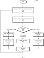
- FIG. 5 is a flow diagram of one embodiment of a method for operating a tracking ADC.
- Method 500 may be carried out by any of the tracking ADC embodiments discussed above.
- embodiments of a tracking ADC that are capable of carrying out Method 500 are also considered to fall within the scope of this disclosure.
- Method 500 includes generating, by a feedback circuit and based on an input voltage, a feedback signal (block 505 ).
- the method further includes sampling, by a comparison circuit and using a plurality of threshold voltages, the feedback signal to generate a plurality of samples (block 510 ).
- the tracking ADC includes a counter circuit, and thus, Method 500 further includes updating a count value, by a counter circuit, based on a subset of the plurality of samples (block 515 ), and generating, using a digital-to-analog circuit, a control signal based on the count value (block 520 ).
- Method 500 further includes modifying the feedback signal using the control signal and at least one of the plurality of samples (block 525 ).
- the method includes generating a first comparison signal, using a first comparator circuit, in response to determining that a voltage of the feedback signal exceeds a first threshold, and activating a first current source to modify the feedback signal based on determining a voltage of the feedback signal exceeds the first threshold.
- the embodiment may also include a second comparator circuit, and thus the method may include generating a second comparison signal, using a second comparator circuit, in response to determining that the voltage of the feedback signal is less than a second threshold, wherein the second threshold is less than the first threshold, and activating a second current source to modify the feedback signal based on determining that the voltage of the feedback signal is less than the second threshold.
- the voltage of the feedback signal may be greater than the second threshold and less than the first threshold.
- embodiments of the method include inhibiting activation of the first and second current sources in response to the voltage of the feedback signal being less than the first threshold and greater than the second threshold.
- embodiments of the method include incrementing the count value in response to the first comparator circuit asserting the first comparator signal, and decrementing the count value in response to the second comparator asserting the second comparator signal.
- the method may further include maintaining the count value in response to neither the first comparator circuit asserting the first comparator signal nor the second comparator asserting the second comparator signal.
- embodiments of a method for operating such a tracking ADC include modifying the feedback signal, during a first portion of a given clock cycle, using at least one of the plurality of samples and the control signal, and further include modifying the feedback signal, during a second portion of the given clock cycle, using the control signal exclusive of the feedback signal.
- embodiments of the method include modifying the feedback signal by a value corresponding to one least significant bit of the counter circuit. That is, the voltage change of the feedback signal may be substantially or approximately the same amount that, when applied to comparison circuitry, would cause the counter output to change by one least significant bit.
- FIG. 6 is a flow diagram of another embodiment of a method for operating a tracking ADC.
- Method 600 may be carried out by a tracking ADC such as that shown in FIG. 2 , as well as other types of tracking ADCs that perform comparisons of a feedback voltage to two different thresholds and either increment, decrement, or maintain the count value for a given sample.
- Embodiments of a tracking ADC capable of carrying out Method 600 but not otherwise disclosed herein are considered to fall within the scope of this disclosure.
- the application of a tracking ADC in the embodiment of Method 600 as discussed herein is supply voltage monitoring, although method embodiments involving other use cases may also be considered to fall within the scope of this disclosure.
- Method 600 includes generating a feedback voltage based on a monitored supply voltage (block 605 ).
- the feedback voltage is then compared to various threshold voltages (block 610 ).
- the tracking ADC may include a first comparator circuit that compares the feedback voltage to a first threshold voltage, and a second comparator circuit that compares the feedback voltage to a second threshold voltage that is less than the first threshold voltage.
- the feedback voltage is less than the first threshold voltage but greater than the second threshold voltage (block 615 , Vfb ⁇ V_thrsh_U, Vfb>V_thrsh_D), then the current count value is maintained by the counter circuit (block 620 ). That is, the counter is neither incremented or decremented.
- a feedback circuit of the tracking ADC may modify Vfb downward by an amount approximately or substantially equivalent to on LSB (block 625 ). In one embodiment, this may be carried out by injecting current into the same node of the circuit upon which the feedback voltage is conveyed. Additionally, in response to the comparison result, the counter is incremented and, after a certain amount of time, the modification of the feedback voltage is discontinued (block 630 ). In one embodiment, this amount of time may be after a sufficient amount of time has elapsed to ensure that the settling of the voltage of the feedback voltage.
- the feedback circuit of the tracking ADC may modify Vfb upward by one LSB (block 635 ). Thereafter, the count value from the counter circuit is decremented, and the modification of Vfb may be discontinued after sufficient time has elapsed.
- Method 600 after incrementing, decrementing, or maintaining the count value for a given sample, the method may progress to a next sample (block 645 ) and return to block 605 .
- the system 700 includes at least one instance of a system on chip (SoC) 706 which may include multiple types of processing units, such as a central processing unit (CPU), a graphics processing unit (GPU), or otherwise, a communication fabric, and interfaces to memories and input/output devices.
- SoC system on chip
- processors in SoC 706 includes multiple execution lanes and an instruction issue queue.
- SoC 706 is coupled to external memory 702 , peripherals 704 , and power supply 708 .
- a power supply 708 is also provided which supplies the supply voltages to SoC 706 as well as one or more supply voltages to the memory 702 and/or the peripherals 704 .
- power supply 708 represents a battery (e.g., a rechargeable battery in a smart phone, laptop or tablet computer, or other device).
- more than one instance of SoC 706 is included (and more than one external memory 702 is included as well).
- the memory 702 is any type of memory, such as dynamic random access memory (DRAM), synchronous DRAM (SDRAM), double data rate (DDR, DDR2, DDR3, etc.) SDRAM (including mobile versions of the SDRAMs such as mDDR3, etc., and/or low power versions of the SDRAMs such as LPDDR2, etc.), RAMBUS DRAM (RDRAM), static RAM (SRAM), etc.
- DRAM dynamic random access memory
- SDRAM synchronous DRAM
- DDR double data rate
- DDR double data rate
- RDRAM RAMBUS DRAM
- SRAM static RAM
- One or more memory devices are coupled onto a circuit board to form memory modules such as single inline memory modules (SIMMs), dual inline memory modules (DIMMs), etc.
- SIMMs single inline memory modules
- DIMMs dual inline memory modules
- the devices are mounted with a SoC or an integrated circuit in a chip-on-chip configuration, a package-on-package configuration, or a multi-chip module
- SoC 706 may include a power management circuit configured to managed the power provided to various functional circuit blocks, and may thus also include various instances of a tracking ADC to monitor voltage levels of power converters that provide a supply voltage to these functional circuit blocks.
- peripherals 704 include any desired circuitry, depending on the type of system 700 .
- peripherals 704 includes devices for various types of wireless communication, such as Wi-Fi, Bluetooth, cellular, global positioning system, etc.
- the peripherals 704 also include additional storage, including RAM storage, solid state storage, or disk storage.
- the peripherals 704 include user interface devices such as a display screen, including touch display screens or multitouch display screens, keyboard or other input devices, microphones, speakers, etc.
- system 700 is shown to have application in a wide range of areas.
- system 700 may be utilized as part of the chips, circuitry, components, etc., of a desktop computer 710 , laptop computer 720 , tablet computer 730 , cellular or mobile phone 740 , or television 750 (or set-top box coupled to a television).
- a smartwatch and health monitoring device 760 may include a variety of general-purpose computing related functions.
- smartwatch 760 may provide access to email, cellphone service, a user calendar, and so on.
- a health monitoring device may be a dedicated medical device or otherwise include dedicated health related functionality.
- a health monitoring device may monitor a user's vital signs, track proximity of a user to other users for the purpose of epidemiological social distancing, contact tracing, provide communication to an emergency service in the event of a health crisis, and so on.
- the above-mentioned smartwatch may or may not include some or any health monitoring related functions.
- Other wearable devices are contemplated as well, such as devices worn around the neck, devices that are implantable in the human body, glasses designed to provide an augmented and/or virtual reality experience, and so on.
- System 700 may further be used as part of a cloud-based service(s) 770 .
- the previously mentioned devices, and/or other devices may access computing resources in the cloud (i.e., remotely located hardware and/or software resources).
- system 700 may be utilized in one or more devices of a home other than those previously mentioned.
- appliances within the home may monitor and detect conditions that warrant attention.
- various devices within the home e.g., a refrigerator, a cooling system, etc.
- a thermostat may monitor the temperature in the home and may automate adjustments to a heating/cooling system based on a history of responses to various conditions by the homeowner.
- system 700 may be used in the control and/or entertainment systems of aircraft, trains, buses, cars for hire, private automobiles, waterborne vessels from private boats to cruise liners, scooters (for rent or owned), and so on.
- system 700 may be used to provide automated guidance (e.g., self-driving vehicles), general systems control, and otherwise.
- This disclosure may discuss potential advantages that may arise from the disclosed embodiments. Not all implementations of these embodiments will necessarily manifest any or all of the potential advantages. Whether an advantage is realized for a particular implementation depends on many factors, some of which are outside the scope of this disclosure. In fact, there are a number of reasons why an implementation that falls within the scope of the claims might not exhibit some or all of any disclosed advantages. For example, a particular implementation might include other circuitry outside the scope of the disclosure that, in conjunction with one of the disclosed embodiments, negates or diminishes one or more the disclosed advantages. Furthermore, suboptimal design execution of a particular implementation (e.g., implementation techniques or tools) could also negate or diminish disclosed advantages.
- embodiments are non-limiting. That is, the disclosed embodiments are not intended to limit the scope of claims that are drafted based on this disclosure, even where only a single example is described with respect to a particular feature.
- the disclosed embodiments are intended to be illustrative rather than restrictive, absent any statements in the disclosure to the contrary. The application is thus intended to permit claims covering disclosed embodiments, as well as such alternatives, modifications, and equivalents that would be apparent to a person skilled in the art having the benefit of this disclosure.
- references to a singular form of an item i.e., a noun or noun phrase preceded by “a,” “an,” or “the” are, unless context clearly dictates otherwise, intended to mean “one or more.” Reference to “an item” in a claim thus does not, without accompanying context, preclude additional instances of the item.
- a “plurality” of items refers to a set of two or more of the items.
- a recitation of “w, x, y, or z, or any combination thereof” or “at least one of . . . w, x, y, and z” is intended to cover all possibilities involving a single element up to the total number of elements in the set. For example, given the set [w, x, y, z], these phrasings cover any single element of the set (e.g., w but not x, y, or z), any two elements (e.g., w and x, but not y or z), any three elements (e.g., w, x, and y, but not z), and all four elements.
- w, x, y, and z thus refers to at least one element of the set [w, x, y, z], thereby covering all possible combinations in this list of elements. This phrase is not to be interpreted to require that there is at least one instance of w, at least one instance of x, at least one instance of y, and at least one instance of z.
- labels may precede nouns or noun phrases in this disclosure.
- different labels used for a feature e.g., “first circuit,” “second circuit,” “particular circuit,” “given circuit,” etc.
- labels “first,” “second,” and “third” when applied to a feature do not imply any type of ordering (e.g., spatial, temporal, logical, etc.), unless stated otherwise.
- the phrase “based on” is used to describe one or more factors that affect a determination. This term does not foreclose the possibility that additional factors may affect the determination. That is, a determination may be solely based on specified factors or based on the specified factors as well as other, unspecified factors.
- a determination may be solely based on specified factors or based on the specified factors as well as other, unspecified factors.
- an entity described or recited as being “configured to” perform some tasks refers to something physical, such as a device, circuit, a system having a processor unit and a memory storing program instructions executable to implement the task, etc. This phrase is not used herein to refer to something intangible.
- various units/circuits/components may be described herein as performing a set of tasks or operations. It is understood that those entities are “configured to” perform those tasks/operations, even if not specifically noted.
- circuits may be described in this disclosure. These circuits or “circuitry” constitute hardware that includes various types of circuit elements, such as combinatorial logic, clocked storage devices (e.g., flip-flops, registers, latches, etc.), finite state machines, memory (e.g., random-access memory, embedded dynamic random-access memory), programmable logic arrays, and so on. Circuitry may be custom designed, or taken from standard libraries. In various implementations, circuitry can, as appropriate, include digital components, analog components, or a combination of both. Certain types of circuits may be commonly referred to as “units” (e.g., a decode unit, an arithmetic logic unit (ALU), functional unit, memory management unit (MMU), etc.). Such units also refer to circuits or circuitry.
- ALU arithmetic logic unit
- MMU memory management unit
- circuits/units/components and other elements illustrated in the drawings and described herein thus include hardware elements such as those described in the preceding paragraph.
- the internal arrangement of hardware elements within a particular circuit may be specified by describing the function of that circuit.
- a particular “decode unit” may be described as performing the function of “processing an opcode of an instruction and routing that instruction to one or more of a plurality of functional units,” which means that the decode unit is “configured to” perform this function.
- This specification of function is sufficient, to those skilled in the computer arts, to connote a set of possible structures for the circuit.
- circuits, units, and other elements may be defined by the functions or operations that they are configured to implement.
- the arrangement and such circuits/units/components with respect to each other and the manner in which they interact form a microarchitectural definition of the hardware that is ultimately manufactured in an integrated circuit or programmed into an FPGA to form a physical implementation of the microarchitectural definition.
- the microarchitectural definition is recognized by those of skill in the art as structure from which many physical implementations may be derived, all of which fall into the broader structure described by the microarchitectural definition.
- HDL hardware description language
- Such an HDL description may take the form of behavioral code (which is typically not synthesizable), register transfer language (RTL) code (which, in contrast to behavioral code, is typically synthesizable), or structural code (e.g., a netlist specifying logic gates and their connectivity).
- the HDL description may subsequently be synthesized against a library of cells designed for a given integrated circuit fabrication technology, and may be modified for timing, power, and other reasons to result in a final design database that is transmitted to a foundry to generate masks and ultimately produce the integrated circuit.
- Some hardware circuits or portions thereof may also be custom-designed in a schematic editor and captured into the integrated circuit design along with synthesized circuitry.
- the integrated circuits may include transistors and other circuit elements (e.g.
- the HDL design may be synthesized to a programmable logic array such as a field programmable gate array (FPGA) and may be implemented in the FPGA.
- FPGA field programmable gate array
Landscapes
- Engineering & Computer Science (AREA)
- Theoretical Computer Science (AREA)
- Analogue/Digital Conversion (AREA)
Abstract
Description
Claims (20)
Priority Applications (1)
| Application Number | Priority Date | Filing Date | Title |
|---|---|---|---|
| US17/931,065 US12081226B2 (en) | 2022-09-09 | 2022-09-09 | Feed-forward in tracking analog-to-digital converter |
Applications Claiming Priority (1)
| Application Number | Priority Date | Filing Date | Title |
|---|---|---|---|
| US17/931,065 US12081226B2 (en) | 2022-09-09 | 2022-09-09 | Feed-forward in tracking analog-to-digital converter |
Publications (2)
| Publication Number | Publication Date |
|---|---|
| US20240088909A1 US20240088909A1 (en) | 2024-03-14 |
| US12081226B2 true US12081226B2 (en) | 2024-09-03 |
Family
ID=90140733
Family Applications (1)
| Application Number | Title | Priority Date | Filing Date |
|---|---|---|---|
| US17/931,065 Active 2042-12-13 US12081226B2 (en) | 2022-09-09 | 2022-09-09 | Feed-forward in tracking analog-to-digital converter |
Country Status (1)
| Country | Link |
|---|---|
| US (1) | US12081226B2 (en) |
Citations (5)
| Publication number | Priority date | Publication date | Assignee | Title |
|---|---|---|---|---|
| US4633720A (en) | 1984-12-17 | 1987-01-06 | Dybel Frank Richard | Load monitoring system for progressive dies |
| US7382309B2 (en) * | 2006-01-16 | 2008-06-03 | Samsung Electronics Co., Ltd. | Analog level meter and method of measuring analog signal level |
| US8358231B2 (en) * | 2011-02-21 | 2013-01-22 | Dialog Semiconductor Gmbh | Tracking analog-to-digital converter (ADC) with a self-controlled variable clock |
| US9419611B2 (en) | 2011-01-14 | 2016-08-16 | Infineon Technologies Ag | Low-power activation circuit with motion sensor |
| US10770983B2 (en) | 2018-12-06 | 2020-09-08 | Infineon Technologies Austria Ag | Circuits and methods for secondary-side rectified voltage sensing in isolated switched-mode power converters |
-
2022
- 2022-09-09 US US17/931,065 patent/US12081226B2/en active Active
Patent Citations (5)
| Publication number | Priority date | Publication date | Assignee | Title |
|---|---|---|---|---|
| US4633720A (en) | 1984-12-17 | 1987-01-06 | Dybel Frank Richard | Load monitoring system for progressive dies |
| US7382309B2 (en) * | 2006-01-16 | 2008-06-03 | Samsung Electronics Co., Ltd. | Analog level meter and method of measuring analog signal level |
| US9419611B2 (en) | 2011-01-14 | 2016-08-16 | Infineon Technologies Ag | Low-power activation circuit with motion sensor |
| US8358231B2 (en) * | 2011-02-21 | 2013-01-22 | Dialog Semiconductor Gmbh | Tracking analog-to-digital converter (ADC) with a self-controlled variable clock |
| US10770983B2 (en) | 2018-12-06 | 2020-09-08 | Infineon Technologies Austria Ag | Circuits and methods for secondary-side rectified voltage sensing in isolated switched-mode power converters |
Also Published As
| Publication number | Publication date |
|---|---|
| US20240088909A1 (en) | 2024-03-14 |
Similar Documents
| Publication | Publication Date | Title |
|---|---|---|
| US11594967B2 (en) | Hysteretic current control switching power converter with clock-controlled switching frequency | |
| US11901806B2 (en) | Disconnect switch for boost converter | |
| US9973191B2 (en) | Power saving with dual-rail supply voltage scheme | |
| US10520970B2 (en) | Multi-phase current mode control loop incorporating a distributed transconductance stage | |
| US11594957B2 (en) | Dual-stage boost converter | |
| US11528016B2 (en) | Low latency comparator with local clock circuit | |
| US11755050B2 (en) | Adaptive current mirror circuit for current shaping with temperature | |
| US11569747B2 (en) | Adaptive phase add/shed for a power converter | |
| US11387733B2 (en) | Rapid discharge of power nodes | |
| US12040708B2 (en) | Multi-level power converter with hysteretic control | |
| US11949334B2 (en) | Power converter with DCR sensing circuit having improved noise immunity | |
| US20240088898A1 (en) | Timing Controlled Level Shifter Circuit | |
| US20250267773A1 (en) | High Current, Low Dropout Driver Circuit | |
| US11777398B2 (en) | Pre-charging bootstrapped FET gate | |
| US12081226B2 (en) | Feed-forward in tracking analog-to-digital converter | |
| US20230108239A1 (en) | Switching Power Converter with Mode Transition Control | |
| US20220094340A1 (en) | Low Power Single Retention Pin Flip-Flop with Balloon Latch | |
| US12034372B2 (en) | Reconfigurable multi-phase power converter | |
| US12542485B2 (en) | Bandwidth control in PLL-based power converter | |
| US12346179B2 (en) | Scalable, hierarchical power delivery system | |
| US20250266750A1 (en) | Thermal Mitigation using Current Redistribution | |
| US12451796B2 (en) | Bootstrapped power switch for a negative buck-boost low-side | |
| US11811567B1 (en) | Serial data receiver with decision feedback equalizer with feed forward technique | |
| US20240356507A1 (en) | High Input Impedance Switched-Capacitor Amplifier | |
| WO2024025784A1 (en) | Non-volatile memory power cycle protection mechanism |
Legal Events
| Date | Code | Title | Description |
|---|---|---|---|
| AS | Assignment |
Owner name: APPLE INC., CALIFORNIA Free format text: ASSIGNMENT OF ASSIGNORS INTEREST;ASSIGNORS:SACCOMANNO, GIOVANNI;CELIN, ALBERTO;BUSIGNANI, FABIO;AND OTHERS;SIGNING DATES FROM 20220807 TO 20220825;REEL/FRAME:061052/0207 |
|
| FEPP | Fee payment procedure |
Free format text: ENTITY STATUS SET TO UNDISCOUNTED (ORIGINAL EVENT CODE: BIG.); ENTITY STATUS OF PATENT OWNER: LARGE ENTITY |
|
| STPP | Information on status: patent application and granting procedure in general |
Free format text: DOCKETED NEW CASE - READY FOR EXAMINATION |
|
| STPP | Information on status: patent application and granting procedure in general |
Free format text: NOTICE OF ALLOWANCE MAILED -- APPLICATION RECEIVED IN OFFICE OF PUBLICATIONS |
|
| STPP | Information on status: patent application and granting procedure in general |
Free format text: NOTICE OF ALLOWANCE MAILED -- APPLICATION RECEIVED IN OFFICE OF PUBLICATIONS |
|
| STPP | Information on status: patent application and granting procedure in general |
Free format text: PUBLICATIONS -- ISSUE FEE PAYMENT RECEIVED |
|
| STPP | Information on status: patent application and granting procedure in general |
Free format text: PUBLICATIONS -- ISSUE FEE PAYMENT VERIFIED Free format text: AWAITING TC RESP, ISSUE FEE PAYMENT VERIFIED |
|
| STCF | Information on status: patent grant |
Free format text: PATENTED CASE |