US12080941B2 - Signal transferring device and multiplexer using magnetic thin film structures - Google Patents
Signal transferring device and multiplexer using magnetic thin film structures Download PDFInfo
- Publication number
- US12080941B2 US12080941B2 US17/523,027 US202117523027A US12080941B2 US 12080941 B2 US12080941 B2 US 12080941B2 US 202117523027 A US202117523027 A US 202117523027A US 12080941 B2 US12080941 B2 US 12080941B2
- Authority
- US
- United States
- Prior art keywords
- structures
- path
- signal
- thin film
- magnetic thin
- Prior art date
- Legal status (The legal status is an assumption and is not a legal conclusion. Google has not performed a legal analysis and makes no representation as to the accuracy of the status listed.)
- Active, expires
Links
Images


Classifications
-
- H—ELECTRICITY
- H01—ELECTRIC ELEMENTS
- H01Q—ANTENNAS, i.e. RADIO AERIALS
- H01Q1/00—Details of, or arrangements associated with, antennas
- H01Q1/36—Structural form of radiating elements, e.g. cone, spiral, umbrella; Particular materials used therewith
- H01Q1/38—Structural form of radiating elements, e.g. cone, spiral, umbrella; Particular materials used therewith formed by a conductive layer on an insulating support
-
- G—PHYSICS
- G11—INFORMATION STORAGE
- G11C—STATIC STORES
- G11C11/00—Digital stores characterised by the use of particular electric or magnetic storage elements; Storage elements therefor
- G11C11/02—Digital stores characterised by the use of particular electric or magnetic storage elements; Storage elements therefor using magnetic elements
- G11C11/16—Digital stores characterised by the use of particular electric or magnetic storage elements; Storage elements therefor using magnetic elements using elements in which the storage effect is based on magnetic spin effect
-
- H—ELECTRICITY
- H01—ELECTRIC ELEMENTS
- H01F—MAGNETS; INDUCTANCES; TRANSFORMERS; SELECTION OF MATERIALS FOR THEIR MAGNETIC PROPERTIES
- H01F10/00—Thin magnetic films, e.g. of one-domain structure
- H01F10/08—Thin magnetic films, e.g. of one-domain structure characterised by magnetic layers
- H01F10/10—Thin magnetic films, e.g. of one-domain structure characterised by magnetic layers characterised by the composition
- H01F10/12—Thin magnetic films, e.g. of one-domain structure characterised by magnetic layers characterised by the composition being metals or alloys
- H01F10/14—Thin magnetic films, e.g. of one-domain structure characterised by magnetic layers characterised by the composition being metals or alloys containing iron or nickel
-
- H—ELECTRICITY
- H01—ELECTRIC ELEMENTS
- H01F—MAGNETS; INDUCTANCES; TRANSFORMERS; SELECTION OF MATERIALS FOR THEIR MAGNETIC PROPERTIES
- H01F38/00—Adaptations of transformers or inductances for specific applications or functions
- H01F38/14—Inductive couplings
-
- H—ELECTRICITY
- H04—ELECTRIC COMMUNICATION TECHNIQUE
- H04B—TRANSMISSION
- H04B5/00—Near-field transmission systems, e.g. inductive or capacitive transmission systems
- H04B5/20—Near-field transmission systems, e.g. inductive or capacitive transmission systems characterised by the transmission technique; characterised by the transmission medium
- H04B5/24—Inductive coupling
- H04B5/26—Inductive coupling using coils
-
- H—ELECTRICITY
- H01—ELECTRIC ELEMENTS
- H01F—MAGNETS; INDUCTANCES; TRANSFORMERS; SELECTION OF MATERIALS FOR THEIR MAGNETIC PROPERTIES
- H01F38/00—Adaptations of transformers or inductances for specific applications or functions
- H01F38/14—Inductive couplings
- H01F2038/143—Inductive couplings for signals
-
- H—ELECTRICITY
- H04—ELECTRIC COMMUNICATION TECHNIQUE
- H04L—TRANSMISSION OF DIGITAL INFORMATION, e.g. TELEGRAPHIC COMMUNICATION
- H04L27/00—Modulated-carrier systems
- H04L27/26—Systems using multi-frequency codes
- H04L27/2601—Multicarrier modulation systems
- H04L27/2626—Arrangements specific to the transmitter only
- H04L27/2627—Modulators
- H04L27/2634—Inverse fast Fourier transform [IFFT] or inverse discrete Fourier transform [IDFT] modulators in combination with other circuits for modulation
- H04L27/2636—Inverse fast Fourier transform [IFFT] or inverse discrete Fourier transform [IDFT] modulators in combination with other circuits for modulation with FFT or DFT modulators, e.g. standard single-carrier frequency-division multiple access [SC-FDMA] transmitter or DFT spread orthogonal frequency division multiplexing [DFT-SOFDM]
Definitions
- the present inventive concepts relate to a signal transferring devices and multiplexers using magnetic thin film structures and, more particularly, to signal transferring devices using magnetic thin film structures having low energy consumption and easily-controllable wave characteristics, and multiplexers using magnetic thin film structures capable of performing multiplexing/demultiplexing.
- Data signal multiplexing is a core function that is broadly used for data transmission in communication technology together with computer networks. In various fields of data transmission, it is desired to transmit multiple data signals through a single transmission line. In addition, as means for efficiently transmitting signals through circuits, the possibility of time division and frequency division has been experimentally demonstrated.
- CMOS complementary metal-oxide-semiconductor
- MQCA magnetic quantum-dot cellular automata
- a magnetic vortex has a clockwise (CW) or counterclockwise (CCW) curling magnetization around a vortex core perpendicular to a disk plane.
- CW clockwise
- CCW counterclockwise
- gyrotropic motion of the vortex core may be excited in a unique mode.
- a coupled mode or coupled gyration mode thereof is present.
- magnetic vortex or skyrmion structure is expected to be applicable to data processing such as communication devices, memory devices, and logic devices in the future.
- the present inventive concepts provide selective signal transferring and/or reliable signal transferring control in regard to existing technology using the vortex or skyrmion structure and/or with regard to applications to signal transferring in a coupled mode.
- the present inventive concepts provide a signal transferring device and multiplexer using magnetic thin film structures having low energy consumption and easily-controllable wave characteristics.
- the present inventive concepts also provide a signal transferring device using magnetic thin film structures capable of selectively and reliably transferring signals.
- the present inventive concepts also provides a multiplexer using magnetic thin film structures capable of performing time-division multiplexing/demultiplexing and frequency-division multiplexing/demultiplexing.
- a signal transferring device may include a first structure that includes a first magnetic thin film structure having a first magnetic vortex configured to receive a signal as an input signal, a second structure that is spaced apart from at least one side of the first structure, the second structure including a second magnetic thin film structure having a second magnetic vortex configured to transfer the signal, and a third structure that is spaced apart from at least one side of the second structure, the third structure including a third magnetic thin film structure having a third magnetic vortex configured to output the signal from the signal transferring device.
- the first and third structures may have a symmetrical shape
- the second structure may have an asymmetrical shape.
- a multiplexer may include a signal inputter at respective first ends of a plurality of paths; and a separate signal outputter at a second end of each path of the plurality of paths.
- a first structure that includes a first magnetic thin film structure may be on the signal inputter, At least one structure of second structures and third structures may be on each path extending to the separate signal outputter of the path.
- Each second structure of the second structures may include a separate second magnetic thin film structure.
- Each third structure of the third structures may include a separate third magnetic thin film structure.
- the first and third structures may each have a symmetrical shape and the second structure may have an asymmetrical shape.
- the first and third structures may have a disk shape and the second structure may have a separate disk shape including at least one asymmetrical portion.
- the separate disk shape may include at least one flat edge.
- An asymmetrical portion of the second structure may face the third structure.
- the first, second, and third structures may have equal in-plane curling magnetizations.
- a vortex core of the first structure may exhibit three coupled modes when an in-plane magnetic bias field is applied in a y axis direction, and exhibit two coupled modes when an in-plane magnetic bias field is applied in a ⁇ y axis direction.
- an input signal of the first structure may be transferred via the second structure to the third structure when an in-plane magnetic bias field is applied in a y axis direction, and not be transferred to the third structure when a magnetic field is applied in a ⁇ y axis direction.
- Resonant frequencies of the first and third structures may increase when vortex cores are shifted outward from disk centers, and a resonant frequency of the second structure may decrease when a vortex core is shifted outward from a disk center.
- FIGS. 1 A and 1 B are schematic diagrams showing types of magnetic thin film structures according to some example embodiments of the present inventive concepts
- FIG. 2 includes graphs showing fast Fourier transformation (FFT) power of magnetic thin film structures according to some example embodiments of the present inventive concepts, depending on a bias field;
- FFT fast Fourier transformation
- FIGS. 3 A and 3 B include graphs showing variations in gyrotropic resonant frequencies of magnetic thin film structures according to some example embodiments of the present inventive concepts, depending on the intensity of an in-plane magnetic bias field;
- FIGS. 4 A, 4 B, and 4 C are schematic diagrams showing operation of a signal transferring device according to some example embodiments of the present inventive concepts
- FIG. 5 is a schematic diagram of signal transferring devices according to some example embodiments of the present inventive concepts and a comparative example
- FIG. 6 includes graphs showing FFT power of signal transferring devices according to some example embodiments of the present inventive concepts and a comparative example, depending on a bias field;
- FIG. 7 is a schematic diagram showing orbits of cores of signal transferring devices according to some example embodiments of the present inventive concepts and a comparative example, depending on a bias field;
- FIG. 8 includes graphs showing the amplitudes of gyration signals of first and third structures of signal transferring devices according to some example embodiments of the present inventive concepts and a comparative example;
- FIG. 9 includes graphs showing the amplitudes of gyration signals of first and third structures of signal transferring devices according to some example embodiments of the present inventive concepts and a comparative example, depending on a frequency;
- FIGS. 10 A and 10 B include a schematic diagram and a truth table of a demultiplexer
- FIGS. 11 A, 11 B, and 11 C are schematic diagrams showing operation of a multiplexer/demultiplexer according to some example embodiments of the present inventive concepts
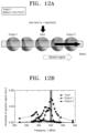
- FIGS. 12 A, 12 B, 13 A, and 13 B include graphs showing signal transferring and the amplitudes of gyration signals in a signal inputter and signal outputters depending on a frequency and a bias field, in a multiplexer/demultiplexer according to some example embodiments of the present inventive concepts;
- FIGS. 14 A and 14 B include graphs showing signal transferring and the amplitudes of gyration signals in a signal inputter and signal outputters depending on a frequency and a bias field, in a multiplexer/demultiplexer according to some example embodiments of the present inventive concepts.
- FIG. 15 is a schematic view of an electronic device according to some example embodiments.
- elements and/or properties thereof e.g., structures, surfaces, directions, or the like
- elements and/or properties thereof which may be referred to as being “perpendicular,” “parallel,” “coplanar,” or the like with regard to other elements and/or properties thereof (e.g., structures, surfaces, directions, or the like) may be “perpendicular,” “parallel,” “coplanar,” or the like or may be “substantially perpendicular,” “substantially parallel,” “substantially coplanar,” respectively, with regard to the other elements and/or properties thereof.
- Elements and/or properties thereof e.g., structures, surfaces, directions, or the like
- are “substantially perpendicular” with regard to other elements and/or properties thereof will be understood to be “perpendicular” with regard to the other elements and/or properties thereof within manufacturing tolerances and/or material tolerances and/or have a deviation in magnitude and/or angle from “perpendicular,” or the like with regard to the other elements and/or properties thereof that is equal to or less than 10% (e.g., a. tolerance of ⁇ 10%).
- Elements and/or properties thereof e.g., structures, surfaces, directions, or the like
- are “substantially parallel” with regard to other elements and/or properties thereof will be understood to be “parallel” with regard to the other elements and/or properties thereof within manufacturing tolerances and/or material tolerances and/or have a deviation in magnitude and/or angle from “parallel,” or the like with regard to the other elements and/or properties thereof that is equal to or less than 10% (e.g., a. tolerance of ⁇ 10%).
- Elements and/or properties thereof that are “substantially identical” to, “substantially the same” as or “substantially equal” to other elements and/or properties thereof will be understood to include elements and/or properties thereof that are identical to, the same as, or equal to the other elements and/or properties thereof within manufacturing tolerances and/or material tolerances.
- Elements and/or properties thereof that are identical or substantially identical to and/or the same or substantially the same as other elements and/or properties thereof may be structurally the same or substantially the same, functionally the same or substantially the same, and/or compositionally the same or substantially the same.
- FIGS. 1 A and 1 B are schematic diagrams showing types of magnetic thin film structures according to some example embodiments of the present inventive concepts.
- the magnetic thin film structures used to implement a signal transferring device may include two types.
- the magnetic thin film structures may include two types such as a first structure 10 having a disk shape as illustrated in FIG. 1 B , and a second structure 20 obtained by modifying the symmetrical first structure 10 to include an asymmetrical portion or at least one flat edge 21 as illustrated in FIG. 1 A .
- a disk-type structure including at least one flat edge will be described as an example of a structure including an asymmetrical portion.
- the shape of the second structure 20 is not limited thereto.
- Any disk shape having an off-centered core e.g., a disk shape including at least one portion having a curvature different from that of the other portion or a disk shape including a plurality of edges, may be included in the asymmetrical structure, and even a polygonal shape including an asymmetrical portion may also be included in the asymmetrical structure.
- a third structure 30 to be described below may have the same shape or substantially the same shape as the first structure 10 .
- the first structure 10 is also referred to as a ‘circular disk’ and the second structure 20 is also referred to as a ‘chopped disk’.
- the magnetic thin film structures may be formed using a thin film deposition method such as sputtering, electron beam evaporation, or thermal evaporation.
- the second structure 20 may be formed by a same method used for the first structure 10 and an additional patterning process to include an asymmetrical portion or at least one flat edge 21 .
- the magnetic thin film structures may be made of a ferromagnetic material, e.g., cobalt (Co), iron (Fe), nickel (Ni), Fe—Ni alloy, Fe—Ni—Co alloy, or Fe—Ni-molybdenum (Mo) alloy.
- a ferromagnetic material e.g., cobalt (Co), iron (Fe), nickel (Ni), Fe—Ni alloy, Fe—Ni—Co alloy, or Fe—Ni-molybdenum (Mo) alloy.
- a magnetization structure in a ferromagnetic thin film is determined depending on the shape, thickness, diameter, etc. Particularly, in a cylindrical magnetic film with a diameter of several to several hundred micrometers and a thickness of several ten nanometers, there may exist a magnetic vortex structure at least partially comprising (e.g., consisting of) a core magnetized perpendicularly to a disk plane with a diameter of about 10 nm in a disk center and a clockwise (CW)/counterclockwise (CCW) curling in-plane magnetization around the core.
- a magnetic vortex is can be classified into four types according to its polarity of a core and chirality of a curling magnetization. The vortex has very high thermal and energetic stability.
- the first and second structures 10 and 20 made of permalloy may commonly have a diameter D of 1,000 nm and a thickness of 40 nm and the second structure 20 may have a chopped width E of 150 nm.
- FIG. 2 includes graphs showing fast Fourier transformation (FFT) power of magnetic thin film structures according to some example embodiments of the present inventive concepts, depending on a bias field.
- the graphs show resonant modes of the magnetic thin film structures depending on the bias field.
- FIGS. 3 A and 3 B include graphs showing variations in gyrotropic resonant frequencies of magnetic thin film structures according to some example embodiments of the present inventive concepts, depending on the intensity of an in-plane magnetic bias field.
- micromagnetic simulation code using the Landau-Lifshitz-Gilbert (LLG) equation e.g., oommf or mumax3
- LLG Landau-Lifshitz-Gilbert
- H eff is a total effective field
- M s is a saturation magnetization
- ⁇ is a Gilbert damping constant
- the saturation magnetization M s is 8.0 ⁇ 10 5 A/m
- an exchange stiffness constant A ex is 1.3 ⁇ 10 ⁇ 11 J/m
- the Gilbert damping constant ⁇ is 0.01
- a gyromagnetic ratio ⁇ is 2.21 ⁇ 10 5 m/A ⁇ s
- magnetocrystalline anisotropy is 0.
- a cell size is 5 ⁇ 5 ⁇ 40 nm 3 .
- a vortex Without an external magnetic field, a vortex is energetically stable when a core is placed in a center of the disk. However, when a specific external magnetic field or current is applied, the vortex is off-centered and gyrates. In this case, the vortex core gyrates with a specific eigenfrequency depending on the type and material of the magnetic thin film structure. Therefore, even a low-intensity of an external sinusoidal magnetic field with a resonant frequency can excite a strong gyrotropic motion of a vortex core due to the resonance phenomenon.
- a gyrotropic motion of the vortex core as an input signal from outside may be induced by displacing a vortex core from a center.
- the center refers to a position at which the vortex core is in a stable state without being influenced by an external magnetic field.
- the vortex core of the magnetic thin film structure may be displaced from the center by applying a magnetic field or current to the magnetic thin film structure.
- a method of directly applying a magnetic field to the magnetic thin film structure includes, for example, a method of applying a linear magnetic field.
- a linear magnetic field may be generated by positioning wire on or under the magnetic thin film structure in parallel with the longitude direction of the structure and application of current to the wire.
- the first structure 10 e.g., a circular disk
- the second structure 20 e.g., a chopped disk
- a vortex of each of the first and second structures 10 and 20 is assumed as having an upward core and a counterclockwise (CCW) curling in-plane magnetization.
- a resonant frequency depending on a linear magnetic field H y is identified.
- the resonant frequency of the circular disk increases in proportion to the intensity of the magnetic field as the core is shifted away from the disk center regardless of the direction of the magnetic field, but the resonant frequency of the chopped disk decreases in inverse proportion to the intensity of the magnetic field when the magnetic field is applied in a direction in which the core approaches the flat edge, because dynamic stiffness of the vortex decreases as the core approaches the flat edge.
- a signal transferring device including the first, second, and third structures 10 , 20 , and 30 for example as shown in FIGS.
- the signal transferring device may be configured to cause resonant frequencies of the first and third structures 10 and 30 to increase in response to respective vortex cores of the first and third structures 10 and 30 being shifted outward from respective disk centers of the first and third structures 10 and 30 , and the signal transferring device may be further configured to cause a resonant frequency of the second structure 20 to decrease in response to a vortex core of the second structure 20 being shifted outward from a disk center of the second structure 20 .
- a signal transferring device of the present inventive concepts which is designed by applying the principle described above in relation to FIGS. 1 A to 3 B , will now be described.
- FIGS. 4 A, 4 B, and 4 C are schematic diagram showing operation of a signal transferring device according to some example embodiments of the present inventive concepts.
- the signal transferring device of the present inventive concepts may include the first structure 10 , the second structure 20 , and the third structure 30 positioned to be spaced apart from each other.
- the second structure 20 may be spaced apart from at least one side of the first structure 10
- the third structure 30 may be spaced apart from at least one side of the second structure 20 .
- the first and third structures 10 and 30 may have a symmetrical shape which may be a same shape or substantially a same shape, and the second structure 20 may have an asymmetrical shape.
- first and third structures 10 and 30 may have a disk shape, for example the same circular disk shape or substantially the same circular disk shape
- the second structure 20 may have a disk shape comprising at least one asymmetrical portion, for example a disk shape comprising at least one flat edge, for example a chopped disk shape including the flat edge 21 as shown in FIGS. 4 A- 4 C .
- the first structure 10 may be understood to include a first magnetic thin film structure having a first magnetic vortex
- the second structure 20 may be understood to include a second magnetic thin film structure having a second magnetic vortex
- the third structure 30 may be understood to include a third magnetic thin film structure having a third magnetic vortex.
- the first magnetic thin film structure of the first structure 10 may be configured to receive a signal (e.g., an input signal into the signal transferring device)
- the second magnetic thin film structure of the second structure 20 having a second magnetic vortex
- the third magnetic thin film structure of the third structure 30 having a third magnetic vortex
- the signal transferring device of the present inventive concepts is characterized in that a signal is input to the first structure 10 and a signal output from the third structure 30 is controlled according to the core motion of the second structure 20 .
- FIGS. 4 A to 4 C illustrate the simplest example of signal transferring device comprising the first, second, and third structures 10 , 20 , and 30
- a signal transferring device including any combination of shape, structure, size, etc. of the first, second, and third structures 10 , 20 , and 30 may be implemented, as long as at least one second structure 20 .
- the magnetic thin film structures may be arranged in a straight or curved line, in a two-dimensional planar structure, or in a three-dimensional shape.
- Gyrotropic motion of a vortex core of the first structure 10 may cause gyrotropic motion of a core of the second structure 20
- the gyrotropic motion of the core of the second structure 20 may cause gyrotropic motion of a core of the third structure 30 , thereby the signal of gyrotropic motion in the first structure 10 is transferred to the third structure 30 through the second structure 20 .
- gyrotropic motion of a vortex core may occur then it may cause gyrotropic motion of a vortex core in a neighboring magnetic thin film structure and thus the signal may be transferred.
- Interaction between neighboring vortices is caused by dipole-dipole interaction between the vortices.
- a shift of a vortex core from a disk center in a magnetic thin film structure induces effective magnetization inside the magnetic thin film structure and a stray field around it.
- the stray field interacts to the neighboring magnetic structure, resulting the changes in the magnetization and the energy state of a neighboring magnetic structure.
- the stray field Due to gyration of the vortex core, the stray field also rotates at the same frequency of the vortex core but in an opposite direction of core gyration.
- the gyrating stray field interacts with a vortex core in another neighboring disk-type magnetic thin film structure and causes gyrotropic motion of the vortex core in the neighboring magnetic thin film structure. Therefore, when gyrotropic motion of a vortex core is excited by using an external magnetic field or current, vortex cores in neighboring disk are affected by the stray field and their positions are sequentially shifted by the dipole-dipole interaction, thereby the initial gyrotropic motion of vortex core is propagated to neighboring vortex cores.
- a high-amplitude signal may be generated at low input power by using resonance of a unique mode of the vortex. That is, by forming a magnetic field having a frequency equal to an eigenfrequency of a vortex core in a magnetic thin film structure and applying it to the magnetic thin film structure, a high-amplitude signal of core gyration can be obtained using the resonance phenomenon even with a small amount of energy.
- a gyration signal may be easily transferred from the first structure 10 to the second structure 20 , and be also easily transferred again from the second structure 20 to the third structure 30 .
- a gyration signal may be easily transferred from the first structure 10 to the second structure 20 , and be transferred again from the second structure 20 to the third structure 30 because the first, second, and third structures 10 , 20 , and 30 have almost equal resonant frequencies (see FIG. 2 ).
- a gyration signal may not be transferred from the first structure 10 to the second structure 20 , and transferring of the signal from the second structure 20 to the third structure 30 is also suppressed because the resonant frequencies of the first and third structures 10 and 30 are different from that of the second structure 20 (see FIG. 2 ).
- the flat edge 21 of the second structure 20 may be positioned to face the third structure 30 , for example as shown in FIGS. 4 A- 4 C . Restated, and as shown in FIGS.
- the asymmetrical portion of the second structure 20 may face the third structure 30 , for example such that the flat edge 21 is a proximate edge of the second structure 20 in relation to the third structure 30 .
- the signal transferring device of the present inventive concepts may control signal transferring depending on the resonant frequencies of the first and second structures 10 and 20 by using the difference between FIGS. 4 A, 4 B, and 4 C .
- FIGS. 4 A, 4 B, and 4 C For example, referring to the first, second, and third structures 10 , 20 , and 30 as described herein and as shown in FIGS.
- the respective first, second, and third magnetic thin film structures of the first, second, and third structures 10 , 20 , and 30 may be located on an xy plane such that the xy plane, and the signal transferring device that includes the first, second, and third structures 10 , 20 , and 30 may be configured to cause an input signal received at the first structure 10 to be transferred via the second structure 20 to the third structure 30 in response to a magnetic field being applied to the first, second, and third magnetic thin film structures in a +y axis direction in relation to the xy plane (e.g., in response to H y >0 mT), and to cause the input signal received at the first structure 10 to not be transferred to the third structure 30 (e.g., not to be transferred from the first structure 10 to the third structure 30 via the second structure 20 ) in response to a magnetic field being applied to the first, second, and third magnetic thin film structures in a ⁇ y axis direction in relation
- FIG. 5 is a schematic diagram of signal transferring devices according to some example embodiments of the present inventive concepts and a comparative example.
- three permalloy (Py: Ni 81 Fe 19 ) magnetic thin film structures having a diameter D of 1,000 nm, a thickness t of 40 nm, and a disk interval D int of 100 nm are used.
- the signal transferring device may be obtained by positioning the first structure 10 , the second structure 20 , and the third structure 30 as illustrated in an upper part of FIG. 5 , wherein the second structure 20 has a chopped disk shape, and be referred to as “Type I”.
- the signal transferring device according to the comparative example may be obtained by positioning the first structure 10 , a second structure 20 ′, and the third structure 30 as illustrated in a lower part of FIG. 5 , wherein the second structure 20 ′ has the same circular disk shape as the first and third structures 10 and 30 , and be referred to as “Type II”.
- FIG. 6 includes graphs showing FFT power of the signal transferring devices according to some example embodiments of the present inventive concepts and the comparative example, depending on a bias field.
- the graphs show coupled modes depending on the bias field.
- an initial disk-centered core is shifted in a +y direction by applying a static magnetic field to the first structure 10 in a +x direction. After releasing the magnetic field, the core position of each structure is monitored and its FFT analysis is performed.
- the signal transferring device may be configured to cause resonant frequencies of the first and third structures 10 and 30 to increase in response to respective vortex cores of the first and third structures 10 and 30 being shifted outward from respective disk centers of the first and third structures 10 and 30 , and the signal transferring device may be further configured to cause a resonant frequency of the second structure 20 to decrease in response to a vortex core of the second structure 20 being shifted outward from a disk center of the second structure 20 .
- FIG. 7 is a schematic diagram showing orbits of cores of the signal transferring devices according to some example embodiments of the present inventive concepts and the comparative example, depending on a bias field. The orbits are enlarged five times for convenience of explanation.
- Gyration signal propagation in Type I and Type II will now be described depending on the orbits of the cores.
- a gyration signal is excited by applying a sinusoidal field of 0.2 mT only to the first structure on the left side.
- FIG. 8 includes graphs showing the amplitudes of gyration signals of the first and third structures 10 and 30 of the signal transferring devices according to some example embodiments of the present inventive concepts and the comparative example.
- the amplitudes of the gyration signals are compared depending on variations in x-direction magnetization (the y axis of the graph) according to time (the x axis of the graph).
- FIG. 9 includes graphs showing the amplitudes of gyration signals of the first and third structures 10 and 30 of the signal transferring devices according to some example embodiments of the present inventive concepts and the comparative example, depending on a frequency.
- the amplitude of the gyration signal depends on the frequency of a sinusoidal field.
- Type I and Type II show that the gyration signal of the first structure 10 (see “Disk 1”) exhibits a peak near a coupled mode frequency under the corresponding bias field. It is shown that the gyration signal propagates well near a specific frequency in most cases.
- FIGS. 10 A and 10 B include a schematic diagram and a truth table of a demultiplexer.
- FIGS. 10 A and 10 B illustrate a simple model for receiving one input signal Input and selecting one of two output signals Output 1 and Output 2.
- the output signal Output 1 or Output 2 may have a value 0 or 1 by controlling the input signal Input and a select line.
- FIGS. 11 A, 11 B, and 11 C are schematic diagrams showing operation of a multiplexer/demultiplexer 100 according to some example embodiments of the present inventive concepts.
- the following description is focused, as an example, on a demultiplexer for dividing a signal in a signal reception step, but is also applicable to a multiplexer for selecting a signal in a signal transmission step. Accordingly, it will be understood that a “multiplexer,” “demultiplexer,” and/or “multiplexer/demultiplexer” as described herein with regard to some example embodiments may, in some example embodiments, be a “multiplexer,” a “demultiplexer,” and/or a “multiplexer/demultiplexer.”
- a first structure 110 may be configured the same or substantially the same as the first structure 10
- third structures 120 and 130 may be configured the same or substantially the same as the first structure 110
- Second structures 140 and 150 having flat edges 141 and 151 may be configured the same or substantially the same as the second structure 20 .
- the first structure 110 may be used as a signal inputter of the demultiplexer 100 .
- the second and third structures 120 , 130 , 140 , and 150 may be positioned along a plurality of paths from the first structure 110 , and signal outputters may be positioned at the ends of the paths. Accordingly, it will be understood that a signal inputter may be positioned at respective ends (e.g., respective first ends) of a plurality of paths, and the first structure 110 (which may include a first magnetic thin film structure as described herein according to any example embodiments) may be on the signal inputter.
- the third structures 120 and 130 or the second structures 140 and 150 may be used as the signal outputters (e.g., may be configured to cause signals to be output from the demultiplexer). Accordingly, it will be understood that a separate signal outputter may be positioned at a second end of each path of the plurality of paths, where the second end is opposite from the first end of the path (at which the signal inputter is positioned), and at least one structure of the third structures 120 and 130 and/or the second structures 140 and 150 may be on each path extending to at least one separate signal outputter, such that (as shown in FIGS.
- each separate path from the first end thereof may include at least one second structure of the second structures 140 and 150 and at least one third structure of the third structures 120 and 130 .
- example embodiments are not limited thereto.
- At least one path may include a plurality of second structures and no third structures. In another example, in some example embodiments at least one path may include a plurality of second structures and at least one third structure. In another example, in some example embodiments at least one path may include a plurality of third structures and no second structures. In another example, in some example embodiments at least one path may include a plurality of third structures and at least one second structure.
- the second structures 140 and 150 may include respective second magnetic thin film structures as described herein according to any example embodiments, and the third structures 120 and 130 may include respective third magnetic thin film structures as described herein according to any example embodiments. The number (e.g., quantity) of third structures 120 and 130 or second structures 140 and 150 may vary.
- the first and third structures 110 , 120 , and 130 may each have a symmetrical shape (e.g., a same circular disk shape as shown), and the second structures 140 and 150 may have an asymmetrical shape (e.g., a same chopped disk shape as shown).
- the first and third structures 110 , 120 , and 130 may each have a disk shape (e.g., a same disk shape) and the second structures may have (e.g., may each have) a disk shape comprising at least one asymmetrical portion (e.g., a disk shape comprising at least one flat edge).
- a symmetrical shape e.g., a same circular disk shape as shown
- the second structures 140 and 150 may have an asymmetrical shape (e.g., a same chopped disk shape as shown).
- the first and third structures 110 , 120 , and 130 may each have a disk shape (e.g., a same disk shape) and the second structures may have (e.g., may each have) a
- one second structure e.g., second structure 140 or second structure 150
- one third structure e.g., third structure 120 or third structure 130
- the one third structure may be on the signal outputter of the respective path.
- the first structure 110 e.g., the signal inputter
- the second and third structures 140 and 120 , or 150 and 130 are sequentially positioned along each path.
- the two paths are connected in a straight line to face each other, and the third structures 120 and 130 positioned at the ends of the paths may be used as the signal outputters.
- the flat edges 141 and 151 of the second structures 140 and 150 may be positioned to face the third structures 120 and 130 , such that, in each path, an asymmetrical portion of one second structure therein (e.g., flat edge 141 of second structure 140 ) may face one third structure therein (e.g., third structure 120 ).
- An electrode may be connected along each path to form a magnetic field or current flow.
- a plurality of paths may include two paths that are connected in a straight line to face each other (e.g., extend along a common axis in opposite directions), where the two paths including a first path and a second path, the first structure 110 may be positioned between the first path and the second path, a first set of second and third structures (e.g., 120 and 140 ) may be sequentially spaced apart from each other along the first path from the first structure 110 , and a second set of second and third structures (e.g., 150 and 130 ) may be sequentially spaced apart from each other along the second path from the first structure 110 .
- a gyration signal may be transferred from the first structure 110 to the second structure 150 along a second path (e.g., a rightward direction), and be transferred again from the second structure 150 to the third structure 130 .
- a second path e.g., a rightward direction
- the first, second, and third magnetic thin film structures of the first to third structures 110 , 120 , 130 , 140 , and 150 may be located on an xy plane such that the xy plane intersects each of the first, second, and third magnetic thin film structures, and the demultiplexer 100 may be configured to cause an input signal received at the first structure 110 to be transferred via a second structure of the second path (e.g., second structure 150 ) to a third structure of the second path (e.g., third structure 130 ), along the second path, in response to a magnetic field being applied to the first, second, and third magnetic thin film structures in a +y axis direction in relation to the xy plane.
- a second structure of the second path e.g., second structure 150
- a third structure of the second path e.g., third structure 130
- a gyration signal may not be transferred from the first structure 110 to the second structure 140 along a first path (e.g., a leftward direction), and transferring of the signal from the second structure 140 to the third structure 120 is also suppressed.
- This principle is the same as that described above in relation to FIG. 4 C . Accordingly, and as shown in FIG.
- the first, second, and third magnetic thin film structures of the first to third structures 110 , 120 , 130 , 140 , and 150 may be located on an xy plane such that the xy plane intersects each of the first, second, and third magnetic thin film structures
- the demultiplexer 100 may be configured to cause the input signal received at the first structure 110 to be transferred via a second structure of the first path (e.g., second structure 140 ) to a third structure of the first path (e.g., third structure 120 ), along the first path, in response to a magnetic field being applied to the first, second, and third magnetic thin film structures in a ⁇ y axis direction in relation to the xy plane.
- the input signal Input of the first structure 110 is output from the third structure 130 as the output signal Output 2 and is not output from the third structure 120 as the output signal Output 1.
- cores of all magnetic thin film structures may gyrate while being shifted rightward from disk centers.
- a signal is input to the first structure 110 , along the first path (e.g., the leftward direction), a gyration signal may be transferred from the first structure 110 to the second structure 140 , and be transferred again from the second structure 140 to the third structure 120 .
- This principle is the same as that described above in relation to FIG. 4 B .
- a gyration signal may not be transferred from the first structure 110 to the second structure 150 , and transferring of the signal from the second structure 150 to the third structure 130 is also suppressed.
- This principle is the same as that described above in relation to FIG. 4 C .
- the input signal Input of the first structure 110 is output from the third structure 120 as the output signal Output 1 and is not output from the third structure 130 as the output signal Output 2.
- FIGS. 12 A, 12 B, 13 A, and 13 B include graphs showing signal transferring depending on a bias field and the amplitudes of gyration signals of a signal inputter and signal outputters depending on a frequency, in a multiplexer/demultiplexer according to some example embodiments of the present inventive concepts.
- a typical time-division demultiplexer takes one input line and then switches it to any one of a number of individual output lines at a time.
- a sinusoidal field having a frequency range of 335 MHz ⁇ f ⁇ 350 MHz is applied to the first structure 110 , then gyration signals of the third structures 120 and 130 at both ends are checked.
- a direct current (DC) direction of an electrode connected to the disk array e.g., a direction of a bias field
- the input signal of the first structure 110 may be transferred along the second path (e.g., the rightward direction) to the second structure 150 and thus the output signal Output 2 may be output from the third structure 130 .
- a gyration signal ratio of Output 1 to Output 2 in a frequency range of 330 MHz ⁇ f ⁇ 350 MHz corresponds to about 10 dB.
- the input signal of the first structure 110 may be transferred along the first path (e.g., the leftward direction) to the second structure 140 and thus the output signal Output 1 may be output from the third structure 120 .
- a gyration signal ratio of Output 2 to Output 1 in a frequency range of 330 MHz ⁇ f ⁇ 350 MHz corresponds to about 10 dB.
- a channel of data transmission may be switched and a time-division multiplexer/demultiplexer may be implemented according to some example embodiments of the present inventive concepts.
- FIGS. 14 A and 14 B include graphs showing signal transferring depending on a bias field and the amplitudes of gyration signals in a signal inputter and signal outputters depending on a frequency, in a multiplexer/demultiplexer according to some example embodiments of the present inventive concepts.
- the second structures may include a plurality of second structures
- the third structures may include a plurality of third structures
- the plurality of second structures and the plurality of third structures may be on different paths (e.g., leftwards or rightwards paths as shown in FIG. 14 A ) of the plurality of paths.
- FIG. 14 A shows that the second structures may include a plurality of second structures
- the third structures may include a plurality of third structures
- the plurality of second structures and the plurality of third structures may be on different paths (e.g., leftwards or rightwards paths as shown in FIG. 14 A ) of the plurality of paths.
- the plurality of paths may include two paths that are connected in a straight line to face each other (e.g., extend along a common axis in opposite, left and right directions), where the two paths include a first path and a second path, the first structure may be positioned between the first path and the second path, the plurality of second structures may be spaced apart from each other along the first path from the first structure (e.g., the left path shown in FIG. 14 A ) where the first structure may be the centermost structure in FIG. 14 A , and the plurality of third structures may be spaced apart from each other along the second path from the first structure (e.g., the right path shown in FIG. 14 A ). As shown in FIG.
- respective asymmetrical portions of the plurality of second structures may be spaced apart from each other and may face outward in an extension direction of the path away from the first structure (e.g., in the leftward direction away from the first structure which is the centermost structure as shown in FIG. 14 A ).
- the first structure 110 may be positioned between the first path (e.g., the leftward direction) and the second path (e.g., the rightward direction), a plurality of second structures may be positioned to be spaced apart from each other along the first path, and a plurality of third structures may be positioned to be spaced apart from each other along the second path.
- Flat edges of the plurality of second structures may be positioned to face outward in an extension direction of the first path (e.g., the leftward direction).
- H y 15 mT may be fixed and an input signal with varied frequency may be applied to the first structure 110 .
- Cores of all second structures of the first path may be displaced toward the flat edges and thus the structures in the first path may exhibit lower resonant frequencies than the first structure 110 .
- all third structures of the second path e.g., the rightward direction
- the first path may serve as a channel at a frequency f 1
- the second path e.g., the rightward direction
- a gyration signal ratio of Output 1 to Output 2 is 9.25 dB at f 1 and a gyration signal ratio of Output 2 to Output 1 is 13.4 dB at f 2 .
- a multiplexer/demultiplexer may include the first, second, and third magnetic thin film structures of the first to third structures that are located on an xy plane such that the xy plane intersects each of the first, second, and third magnetic thin film structures, and the multiplexer/demultiplexer may be configured to cause a signal to be transferred along the first path or the second path in response to a magnetic field (e.g., H y ) being applied to the first, second, and third magnetic thin film structures in a +y axis direction and/or ⁇ y axis direction in relation to the xy plane, and the multiplexer/demultiplexer may be configured to cause the signal to be transferred along the first path or the second path based on a frequency band of an input signal of the first structure (e.g., the centermost structure shown in FIG.
- a magnetic field e.g., H y
- the multiplexer/demultiplexer may be configured to cause the signal to be transferred along the first path (e.g., leftward path in FIG. 14 A ) in response to a frequency of the input signal of the first structure being a first frequency (e.g., f 1 ), the multiplexer/demultiplexer is configured to cause the signal to be transferred along the second path (e.g., rightward path in FIG. 14 A ) in response to the frequency of the input signal of the first structure being a second frequency (e.g., f 2 ), and the first frequency (e.g., f 1 ) is lower than the second frequency (e.g., f 2 ).
- the first path e.g., leftward path in FIG. 14 A
- the multiplexer/demultiplexer is configured to cause the signal to be transferred along the second path (e.g., rightward path in FIG. 14 A ) in response to the frequency of the input signal of the first structure being a second frequency (e.g., f 2
- a frequency-division multiplexer/demultiplexer may be implemented according to some example embodiments of the present inventive concepts.
- the signal transferring device may switch “on” and “off” propagation of a gyration signal depending on a bias field direction.
- a signal transferring device using magnetic thin film structures having low energy consumption and easily-controllable wave characteristics may be implemented and thus signals may be selectively and reliably transferred.
- a signal transferring device using magnetic thin film structures having low energy consumption and easily-controllable wave characteristics may be implemented.
- signals may be selectively and reliably transferred.
- time-division multiplexing/demultiplexing and frequency-division multiplexing/demultiplexing may be performed.
- FIG. 15 is a schematic view of an electronic device according to some example embodiments.
- an electronic device 1700 may include a processor 1720 , a memory 1730 , and a communication interface 1740 (e.g., an input/output interface) that are electrically coupled together via a bus 1710 .
- the communication interface 1740 may include, for example a wireless network communication transceiver and/or a wired network communication transceiver. Any of the processor 1720 , the memory 1730 , and/or the communication interface 1740 may include any of the signal transferring devices, multiplexers, demultiplexers, and/or multiplexer/demultiplexers according to any of the example embodiments.
- the memory 1730 which may be a non-transitory computer readable medium, may store a program of instructions.
- the processor 1720 may execute the stored program of instructions to perform one or more functions.
- the processor 1720 may be configured to process an input signal received at the electronic device 1700 via the communication interface 1740 and/or generate an output signal to be transmitted from the electronic device 1700 via the communication interface based on such as processing.
- processor 1720 , memory 1730 , or communication interface 1740 may be included in, include, and/or implement one or more instances of processing circuitry such as hardware including logic circuits, a hardware/software combination such as a processor executing software; or any combination thereof.
- said one or more instances of processing circuitry may include, but are not limited to, a central processing unit (CPU), an application processor (AP), an arithmetic logic unit (ALU), a graphic processing unit (GPU), a digital signal processor, a microcomputer, a field programmable gate array (FPGA), a System-on-Chip (SoC) a programmable logic unit, a microprocessor, or an application-specific integrated circuit (ASIC), etc.
- CPU central processing unit
- AP application processor
- ALU arithmetic logic unit
- GPU graphic processing unit
- FPGA field programmable gate array
- SoC System-on-Chip
- any of the memories, memory units, or the like as described herein may include a non-transitory computer readable storage device, for example a solid state drive (SSD), storing a program of instructions, and the one or more instances of processing circuitry may be configured to execute the program of instructions to implement the functionality of some or all of any of the electronic device 1700 , processor 1720 , memory 1730 , communication interface 1740 , or the like (e.g., the functionality of any of the signal transferring devices, multiplexers, any portion thereof, or the like) according to any of the example embodiments as described herein.
- SSD solid state drive
Landscapes
- Engineering & Computer Science (AREA)
- Power Engineering (AREA)
- Computer Networks & Wireless Communication (AREA)
- Signal Processing (AREA)
- Computer Hardware Design (AREA)
- Hall/Mr Elements (AREA)
Abstract
Description
∂M/∂t=−γM×H eff+(α/M s)M×∂M/∂t,
Claims (18)
Applications Claiming Priority (5)
| Application Number | Priority Date | Filing Date | Title |
|---|---|---|---|
| KR10-2020-0152816 | 2020-11-16 | ||
| KR10-2020-0152817 | 2020-11-16 | ||
| KR10-20250-0152817 | 2020-11-16 | ||
| KR1020200152816A KR102517250B1 (en) | 2020-11-16 | 2020-11-16 | Signal transferring device using magnetic thin film structure |
| KR1020200152817A KR102387955B1 (en) | 2020-11-16 | 2020-11-16 | Multiplexer using magnetic thin film structure |
Publications (2)
| Publication Number | Publication Date |
|---|---|
| US20220158337A1 US20220158337A1 (en) | 2022-05-19 |
| US12080941B2 true US12080941B2 (en) | 2024-09-03 |
Family
ID=81588635
Family Applications (1)
| Application Number | Title | Priority Date | Filing Date |
|---|---|---|---|
| US17/523,027 Active 2043-01-17 US12080941B2 (en) | 2020-11-16 | 2021-11-10 | Signal transferring device and multiplexer using magnetic thin film structures |
Country Status (1)
| Country | Link |
|---|---|
| US (1) | US12080941B2 (en) |
Citations (10)
| Publication number | Priority date | Publication date | Assignee | Title |
|---|---|---|---|---|
| US20040094778A1 (en) * | 2002-10-31 | 2004-05-20 | Renesas Technology Corp. | Semiconductor device and semiconductor memory device provided with internal current setting adjustment circuit |
| US6807092B1 (en) * | 2003-06-13 | 2004-10-19 | Infineon Technologies Ag | MRAM cell having frustrated magnetic reservoirs |
| US20040219956A1 (en) * | 2003-02-06 | 2004-11-04 | Hiroshi Iwai | Portable radio communication apparatus provided with a boom portion and a part of housing operating as an antenna |
| US7187578B2 (en) * | 2002-10-03 | 2007-03-06 | Yang-Ki Hong | Magnetic elements having unique shapes |
| KR20070036673A (en) | 2005-09-29 | 2007-04-03 | 재단법인서울대학교산학협력재단 | Ultra-high speed information processing spin wave device using strong spin wave generation method and spin wave |
| KR20160004838A (en) | 2014-07-04 | 2016-01-13 | 울산과학기술원 산학협력단 | Unit memory device and memory device for writing of information using asymmetry nano disc |
| US20170277046A1 (en) * | 2014-08-29 | 2017-09-28 | Asml Holding N.V. | Method and apparatus for spectrally broadening radiation |
| US20200075233A1 (en) * | 2018-08-30 | 2020-03-05 | Ferric Inc. | Compact Transceiver on a Multi-Level Integrated Circuit |
| US20210099027A1 (en) * | 2019-09-27 | 2021-04-01 | Apple Inc. | Magnetic alignment systems with nfc for electronic devices |
| US20220393349A1 (en) * | 2019-10-30 | 2022-12-08 | Lg Electronics Inc. | Electronic device provided with 5g antenna |
-
2021
- 2021-11-10 US US17/523,027 patent/US12080941B2/en active Active
Patent Citations (11)
| Publication number | Priority date | Publication date | Assignee | Title |
|---|---|---|---|---|
| US7187578B2 (en) * | 2002-10-03 | 2007-03-06 | Yang-Ki Hong | Magnetic elements having unique shapes |
| US20040094778A1 (en) * | 2002-10-31 | 2004-05-20 | Renesas Technology Corp. | Semiconductor device and semiconductor memory device provided with internal current setting adjustment circuit |
| US20040219956A1 (en) * | 2003-02-06 | 2004-11-04 | Hiroshi Iwai | Portable radio communication apparatus provided with a boom portion and a part of housing operating as an antenna |
| US6807092B1 (en) * | 2003-06-13 | 2004-10-19 | Infineon Technologies Ag | MRAM cell having frustrated magnetic reservoirs |
| KR20070036673A (en) | 2005-09-29 | 2007-04-03 | 재단법인서울대학교산학협력재단 | Ultra-high speed information processing spin wave device using strong spin wave generation method and spin wave |
| US20080231392A1 (en) | 2005-09-29 | 2008-09-25 | Sang-Koog Kim | Method of Generating Strong Spin Waves and Spin Devices for Ultra-High Speed Information Processing Using Spin Waves |
| KR20160004838A (en) | 2014-07-04 | 2016-01-13 | 울산과학기술원 산학협력단 | Unit memory device and memory device for writing of information using asymmetry nano disc |
| US20170277046A1 (en) * | 2014-08-29 | 2017-09-28 | Asml Holding N.V. | Method and apparatus for spectrally broadening radiation |
| US20200075233A1 (en) * | 2018-08-30 | 2020-03-05 | Ferric Inc. | Compact Transceiver on a Multi-Level Integrated Circuit |
| US20210099027A1 (en) * | 2019-09-27 | 2021-04-01 | Apple Inc. | Magnetic alignment systems with nfc for electronic devices |
| US20220393349A1 (en) * | 2019-10-30 | 2022-12-08 | Lg Electronics Inc. | Electronic device provided with 5g antenna |
Non-Patent Citations (2)
| Title |
|---|
| Korean Office Action dated Oct. 20, 2021 for corresponding Korean Application No. 10-2020-0152817. |
| Young-Jun Cho, "Dynamics of Magnetic Vortices Coupled in Magnetic Disk Array," Department of Materials Science and Engineering Graduate School Seoul National University, Feb. 2020. |
Also Published As
| Publication number | Publication date |
|---|---|
| US20220158337A1 (en) | 2022-05-19 |
Similar Documents
| Publication | Publication Date | Title |
|---|---|---|
| Bandyopadhyay et al. | Magnetic straintronics: Manipulating the magnetization of magnetostrictive nanomagnets with strain for energy-efficient applications | |
| JP7657453B2 (en) | Spin torque oscillator | |
| Kumar et al. | Magnetic vortex based transistor operations | |
| Serga et al. | YIG magnonics | |
| Berkov et al. | Transition from the macrospin to chaotic behavior by a spin-torque driven magnetization precession of a square nanoelement | |
| Lonsky et al. | Dynamic excitations of chiral magnetic textures | |
| US8908424B2 (en) | Magnetization switching through magnonic spin transfer torque | |
| US12022744B2 (en) | Core magnetization reversal method of skyrmion and data storage device using the method | |
| Shuai et al. | Local anisotropy control of Pt/Co/Ir thin film with perpendicular magnetic anisotropy by surface acoustic waves | |
| Mahato et al. | Configurational anisotropic spin waves in cross-shaped Ni80Fe20 nanoelements | |
| CN109962706B (en) | Spin wave logic device based on Bloch domain wall | |
| US12080941B2 (en) | Signal transferring device and multiplexer using magnetic thin film structures | |
| CN105070824B (en) | A kind of restructural spin wave network of conductors based on neticdomain wall | |
| Gaididei et al. | Switching between different vortex states in two-dimensional easy-plane magnets due to an ac magnetic field | |
| Adhikari et al. | Bias field tunable magnetic configuration and magnetization dynamics in Ni80Fe20 nano-cross structures with varying arm length | |
| US9755652B2 (en) | Nanomagnetic network structures and a method of reconfigurable operation based on magnetization dynamics | |
| Yoo et al. | Excited eigenmodes in magnetic vortex states of soft magnetic half-spheres and spherical caps | |
| Paikaray et al. | Skyrmion dynamics in concentric and eccentric nano-ring structures | |
| CN114639529B (en) | Artificial spinning ice nanostructure and spinning wave transmission regulation and control method | |
| KR102517250B1 (en) | Signal transferring device using magnetic thin film structure | |
| KR102387955B1 (en) | Multiplexer using magnetic thin film structure | |
| KR102159756B1 (en) | Logic device using magnetic thin film structure and operating method thereof | |
| Parreiras et al. | Simulations of magnetic vortex dynamics in exchange-biased sub-micron-sized disks | |
| Cho et al. | Reset-set latch logic operation using vortex-gyration-coupled modes and its driven switching in magnetic-dot networks: A micromagnetic simulation study | |
| Shi et al. | Polarity and chirality modulation of magnetic vortex pair by in-plane magnetic field and surface acoustic waves |
Legal Events
| Date | Code | Title | Description |
|---|---|---|---|
| FEPP | Fee payment procedure |
Free format text: ENTITY STATUS SET TO UNDISCOUNTED (ORIGINAL EVENT CODE: BIG.); ENTITY STATUS OF PATENT OWNER: LARGE ENTITY |
|
| STPP | Information on status: patent application and granting procedure in general |
Free format text: DOCKETED NEW CASE - READY FOR EXAMINATION |
|
| AS | Assignment |
Owner name: SAMSUNG ELECTRONICS CO., LTD., KOREA, REPUBLIC OF Free format text: ASSIGNMENT OF ASSIGNORS INTEREST;ASSIGNORS:KOH, GWAN HYEOB;LEE, KIL HO;KIM, JUN HOE;REEL/FRAME:058572/0894 Effective date: 20211101 Owner name: SEOUL NATIONAL UNIVERSITY R&DB FOUNDATION, KOREA, REPUBLIC OF Free format text: ASSIGNMENT OF ASSIGNORS INTEREST;ASSIGNORS:KIM, SANG KOOG;CHO, YOUNG JUN;SIGNING DATES FROM 20211027 TO 20211103;REEL/FRAME:058572/0878 |
|
| STPP | Information on status: patent application and granting procedure in general |
Free format text: NOTICE OF ALLOWANCE MAILED -- APPLICATION RECEIVED IN OFFICE OF PUBLICATIONS |
|
| ZAAA | Notice of allowance and fees due |
Free format text: ORIGINAL CODE: NOA |
|
| ZAAB | Notice of allowance mailed |
Free format text: ORIGINAL CODE: MN/=. |
|
| STPP | Information on status: patent application and granting procedure in general |
Free format text: AWAITING TC RESP, ISSUE FEE PAYMENT VERIFIED |
|
| STPP | Information on status: patent application and granting procedure in general |
Free format text: PUBLICATIONS -- ISSUE FEE PAYMENT VERIFIED |
|
| STCF | Information on status: patent grant |
Free format text: PATENTED CASE |