US12080799B2 - Semiconductor devices with enhanced substrate isolation - Google Patents
Semiconductor devices with enhanced substrate isolation Download PDFInfo
- Publication number
- US12080799B2 US12080799B2 US17/715,887 US202217715887A US12080799B2 US 12080799 B2 US12080799 B2 US 12080799B2 US 202217715887 A US202217715887 A US 202217715887A US 12080799 B2 US12080799 B2 US 12080799B2
- Authority
- US
- United States
- Prior art keywords
- substrate
- sidewall insulating
- insulating layer
- insulating layers
- semiconductor device
- Prior art date
- Legal status (The legal status is an assumption and is not a legal conclusion. Google has not performed a legal analysis and makes no representation as to the accuracy of the status listed.)
- Active, expires
Links
Images


Classifications
-
- H—ELECTRICITY
- H10—SEMICONDUCTOR DEVICES; ELECTRIC SOLID-STATE DEVICES NOT OTHERWISE PROVIDED FOR
- H10D—INORGANIC ELECTRIC SEMICONDUCTOR DEVICES
- H10D30/00—Field-effect transistors [FET]
- H10D30/60—Insulated-gate field-effect transistors [IGFET]
- H10D30/67—Thin-film transistors [TFT]
- H10D30/6758—Thin-film transistors [TFT] characterised by the insulating substrates
-
- H01L29/78603—
-
- H—ELECTRICITY
- H10—SEMICONDUCTOR DEVICES; ELECTRIC SOLID-STATE DEVICES NOT OTHERWISE PROVIDED FOR
- H10D—INORGANIC ELECTRIC SEMICONDUCTOR DEVICES
- H10D84/00—Integrated devices formed in or on semiconductor substrates that comprise only semiconducting layers, e.g. on Si wafers or on GaAs-on-Si wafers
- H10D84/01—Manufacture or treatment
- H10D84/0123—Integrating together multiple components covered by H10D12/00 or H10D30/00, e.g. integrating multiple IGBTs
- H10D84/0126—Integrating together multiple components covered by H10D12/00 or H10D30/00, e.g. integrating multiple IGBTs the components including insulated gates, e.g. IGFETs
- H10D84/0151—Manufacturing their isolation regions
-
- H01L29/0607—
-
- H—ELECTRICITY
- H10—SEMICONDUCTOR DEVICES; ELECTRIC SOLID-STATE DEVICES NOT OTHERWISE PROVIDED FOR
- H10D—INORGANIC ELECTRIC SEMICONDUCTOR DEVICES
- H10D30/00—Field-effect transistors [FET]
- H10D30/01—Manufacture or treatment
- H10D30/021—Manufacture or treatment of FETs having insulated gates [IGFET]
- H10D30/031—Manufacture or treatment of FETs having insulated gates [IGFET] of thin-film transistors [TFT]
- H10D30/0321—Manufacture or treatment of FETs having insulated gates [IGFET] of thin-film transistors [TFT] comprising silicon, e.g. amorphous silicon or polysilicon
- H10D30/0323—Manufacture or treatment of FETs having insulated gates [IGFET] of thin-film transistors [TFT] comprising silicon, e.g. amorphous silicon or polysilicon comprising monocrystalline silicon
-
- H—ELECTRICITY
- H10—SEMICONDUCTOR DEVICES; ELECTRIC SOLID-STATE DEVICES NOT OTHERWISE PROVIDED FOR
- H10D—INORGANIC ELECTRIC SEMICONDUCTOR DEVICES
- H10D30/00—Field-effect transistors [FET]
- H10D30/60—Insulated-gate field-effect transistors [IGFET]
- H10D30/67—Thin-film transistors [TFT]
- H10D30/6729—Thin-film transistors [TFT] characterised by the electrodes
- H10D30/673—Thin-film transistors [TFT] characterised by the electrodes characterised by the shapes, relative sizes or dispositions of the gate electrodes
-
- H—ELECTRICITY
- H10—SEMICONDUCTOR DEVICES; ELECTRIC SOLID-STATE DEVICES NOT OTHERWISE PROVIDED FOR
- H10D—INORGANIC ELECTRIC SEMICONDUCTOR DEVICES
- H10D30/00—Field-effect transistors [FET]
- H10D30/60—Insulated-gate field-effect transistors [IGFET]
- H10D30/67—Thin-film transistors [TFT]
- H10D30/674—Thin-film transistors [TFT] characterised by the active materials
- H10D30/6741—Group IV materials, e.g. germanium or silicon carbide
- H10D30/6743—Silicon
- H10D30/6744—Monocrystalline silicon
-
- H—ELECTRICITY
- H10—SEMICONDUCTOR DEVICES; ELECTRIC SOLID-STATE DEVICES NOT OTHERWISE PROVIDED FOR
- H10D—INORGANIC ELECTRIC SEMICONDUCTOR DEVICES
- H10D30/00—Field-effect transistors [FET]
- H10D30/60—Insulated-gate field-effect transistors [IGFET]
- H10D30/67—Thin-film transistors [TFT]
- H10D30/6757—Thin-film transistors [TFT] characterised by the structure of the channel, e.g. transverse or longitudinal shape or doping profile
-
- H—ELECTRICITY
- H10—SEMICONDUCTOR DEVICES; ELECTRIC SOLID-STATE DEVICES NOT OTHERWISE PROVIDED FOR
- H10D—INORGANIC ELECTRIC SEMICONDUCTOR DEVICES
- H10D62/00—Semiconductor bodies, or regions thereof, of devices having potential barriers
- H10D62/10—Shapes, relative sizes or dispositions of the regions of the semiconductor bodies; Shapes of the semiconductor bodies
- H10D62/102—Constructional design considerations for preventing surface leakage or controlling electric field concentration
-
- H—ELECTRICITY
- H10—SEMICONDUCTOR DEVICES; ELECTRIC SOLID-STATE DEVICES NOT OTHERWISE PROVIDED FOR
- H10D—INORGANIC ELECTRIC SEMICONDUCTOR DEVICES
- H10D62/00—Semiconductor bodies, or regions thereof, of devices having potential barriers
- H10D62/10—Shapes, relative sizes or dispositions of the regions of the semiconductor bodies; Shapes of the semiconductor bodies
- H10D62/113—Isolations within a component, i.e. internal isolations
- H10D62/115—Dielectric isolations, e.g. air gaps
-
- H—ELECTRICITY
- H10—SEMICONDUCTOR DEVICES; ELECTRIC SOLID-STATE DEVICES NOT OTHERWISE PROVIDED FOR
- H10D—INORGANIC ELECTRIC SEMICONDUCTOR DEVICES
- H10D64/00—Electrodes of devices having potential barriers
- H10D64/20—Electrodes characterised by their shapes, relative sizes or dispositions
- H10D64/27—Electrodes not carrying the current to be rectified, amplified, oscillated or switched, e.g. gates
- H10D64/311—Gate electrodes for field-effect devices
- H10D64/411—Gate electrodes for field-effect devices for FETs
- H10D64/511—Gate electrodes for field-effect devices for FETs for IGFETs
- H10D64/512—Disposition of the gate electrodes, e.g. buried gates
- H10D64/513—Disposition of the gate electrodes, e.g. buried gates within recesses in the substrate, e.g. trench gates, groove gates or buried gates
-
- H—ELECTRICITY
- H10—SEMICONDUCTOR DEVICES; ELECTRIC SOLID-STATE DEVICES NOT OTHERWISE PROVIDED FOR
- H10D—INORGANIC ELECTRIC SEMICONDUCTOR DEVICES
- H10D84/00—Integrated devices formed in or on semiconductor substrates that comprise only semiconducting layers, e.g. on Si wafers or on GaAs-on-Si wafers
- H10D84/01—Manufacture or treatment
- H10D84/0123—Integrating together multiple components covered by H10D12/00 or H10D30/00, e.g. integrating multiple IGBTs
- H10D84/0126—Integrating together multiple components covered by H10D12/00 or H10D30/00, e.g. integrating multiple IGBTs the components including insulated gates, e.g. IGFETs
- H10D84/0135—Manufacturing their gate conductors
-
- H—ELECTRICITY
- H10—SEMICONDUCTOR DEVICES; ELECTRIC SOLID-STATE DEVICES NOT OTHERWISE PROVIDED FOR
- H10D—INORGANIC ELECTRIC SEMICONDUCTOR DEVICES
- H10D84/00—Integrated devices formed in or on semiconductor substrates that comprise only semiconducting layers, e.g. on Si wafers or on GaAs-on-Si wafers
- H10D84/01—Manufacture or treatment
- H10D84/0123—Integrating together multiple components covered by H10D12/00 or H10D30/00, e.g. integrating multiple IGBTs
- H10D84/0126—Integrating together multiple components covered by H10D12/00 or H10D30/00, e.g. integrating multiple IGBTs the components including insulated gates, e.g. IGFETs
- H10D84/0144—Manufacturing their gate insulating layers
-
- H—ELECTRICITY
- H10—SEMICONDUCTOR DEVICES; ELECTRIC SOLID-STATE DEVICES NOT OTHERWISE PROVIDED FOR
- H10D—INORGANIC ELECTRIC SEMICONDUCTOR DEVICES
- H10D86/00—Integrated devices formed in or on insulating or conducting substrates, e.g. formed in silicon-on-insulator [SOI] substrates or on stainless steel or glass substrates
- H10D86/01—Manufacture or treatment
- H10D86/021—Manufacture or treatment of multiple TFTs
- H10D86/0212—Manufacture or treatment of multiple TFTs comprising manufacture, treatment or coating of substrates
-
- H—ELECTRICITY
- H10—SEMICONDUCTOR DEVICES; ELECTRIC SOLID-STATE DEVICES NOT OTHERWISE PROVIDED FOR
- H10D—INORGANIC ELECTRIC SEMICONDUCTOR DEVICES
- H10D86/00—Integrated devices formed in or on insulating or conducting substrates, e.g. formed in silicon-on-insulator [SOI] substrates or on stainless steel or glass substrates
- H10D86/201—Integrated devices formed in or on insulating or conducting substrates, e.g. formed in silicon-on-insulator [SOI] substrates or on stainless steel or glass substrates the substrates comprising an insulating layer on a semiconductor body, e.g. SOI
-
- H—ELECTRICITY
- H10—SEMICONDUCTOR DEVICES; ELECTRIC SOLID-STATE DEVICES NOT OTHERWISE PROVIDED FOR
- H10D—INORGANIC ELECTRIC SEMICONDUCTOR DEVICES
- H10D86/00—Integrated devices formed in or on insulating or conducting substrates, e.g. formed in silicon-on-insulator [SOI] substrates or on stainless steel or glass substrates
- H10D86/40—Integrated devices formed in or on insulating or conducting substrates, e.g. formed in silicon-on-insulator [SOI] substrates or on stainless steel or glass substrates characterised by multiple TFTs
- H10D86/411—Integrated devices formed in or on insulating or conducting substrates, e.g. formed in silicon-on-insulator [SOI] substrates or on stainless steel or glass substrates characterised by multiple TFTs characterised by materials, geometry or structure of the substrates
-
- H—ELECTRICITY
- H10—SEMICONDUCTOR DEVICES; ELECTRIC SOLID-STATE DEVICES NOT OTHERWISE PROVIDED FOR
- H10D—INORGANIC ELECTRIC SEMICONDUCTOR DEVICES
- H10D86/00—Integrated devices formed in or on insulating or conducting substrates, e.g. formed in silicon-on-insulator [SOI] substrates or on stainless steel or glass substrates
- H10D86/40—Integrated devices formed in or on insulating or conducting substrates, e.g. formed in silicon-on-insulator [SOI] substrates or on stainless steel or glass substrates characterised by multiple TFTs
- H10D86/60—Integrated devices formed in or on insulating or conducting substrates, e.g. formed in silicon-on-insulator [SOI] substrates or on stainless steel or glass substrates characterised by multiple TFTs wherein the TFTs are in active matrices
-
- H10P90/1906—
-
- H10W10/012—
-
- H10W10/014—
-
- H10W10/061—
-
- H10W10/13—
-
- H10W10/17—
-
- H10W10/181—
Definitions
- Example embodiments of the present disclosure relate to semiconductor devices and methods of forming same.
- semiconductor devices As the demand for high performance, high speed, and/or multifunctionality of semiconductor devices has increased, the degree of integration of semiconductor devices has concomitantly increased, and a size of transistors within these semiconductor devices has been reduced. Unfortunately, leakage currents associated with these transistors may increase as their size is reduced. To reduce leakage currents, semiconductor devices have been developed using substrates having a silicon-on-insulator (SOI) structure.
- SOI silicon-on-insulator
- An example embodiment of the present disclosure includes a semiconductor device having a transistor therein with improved performance characteristics.
- a semiconductor device in a substrate.
- the semiconductor device includes a substrate insulating structure.
- This substrate insulating structure includes: (i) first sidewall insulating layers, which extend in a first direction and are spaced apart from each other in a second direction perpendicular to the first direction, (ii) second sidewall insulating layers, which extend between the first sidewall insulating layers, and are in contact with the first sidewall insulating layers, and are spaced apart from each other in the first direction, and (iii) a lower insulating layer extending below and in contact with each of the first sidewall insulating layers and the second sidewall insulating layers.
- a gate structure which includes a side surface and a lower surface surrounded by the substrate insulating structure.
- the gate structure includes a gate dielectric layer and a gate electrode on the gate dielectric layer.
- An active region is provided, which extends between the substrate insulating structure and the gate structure.
- a first source/drain region and a second source/drain region are provided, which are spaced apart from each other on the active region.
- the substrate covers an external side surface and a lower surface of the substrate insulating structure.
- a semiconductor device in another example embodiment of the present disclosure, includes a semiconductor substrate, an active region spaced apart from the semiconductor substrate, and a substrate insulating structure embedded in the semiconductor substrate and lining a lower surface and a side surface of the active region.
- a gate structure is provided, which extends on the active region.
- the gate structure includes a gate dielectric layer and a gate electrode on the gate dielectric layer.
- a first source/drain region and a second source/drain region are provided, which are spaced apart from each other on the active region.
- the substrate also covers an external side surface and a lower surface of the substrate insulating structure.
- a semiconductor device which includes a substrate, and a substrate insulating structure embedded in the substrate.
- This substrate insulating structure includes a lower insulating layer, first sidewall insulating layers disposed on the lower insulating layer (and spaced apart from each other), and second sidewall insulating layers disposed on the lower insulating layer and in contact with the first sidewall insulating layers.
- a semiconductor active region is provided, which extends on the lower insulating layer.
- a first source/drain region and a second source/drain region are provided, which are spaced apart from each other on the active region.
- a gate structure is provided, which extends on the active region.
- the gate structure includes a gate dielectric layer and a gate electrode on the gate dielectric layer. At least a portion of the second sidewall insulating layers, the lower insulating layer, and the first sidewall insulating layers are in contact with the substrate.
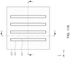
- FIG. 1 is a plan layout view of a semiconductor device according to an example embodiment of the present disclosure
- FIG. 2 is a cross-sectional diagram illustrating a semiconductor device according to an example embodiment of the present disclosure
- FIG. 3 is a cross-sectional diagram illustrating a semiconductor device according to an example embodiment of the present disclosure
- FIG. 4 is a plan layout view of a semiconductor device according to an example embodiment of the present disclosure.
- FIG. 5 is a cross-sectional diagram illustrating a semiconductor device according to an example embodiment of the present disclosure
- FIG. 6 is a plan layout view of a semiconductor device according to an example embodiment of the present disclosure.
- FIG. 7 is a cross-sectional diagram illustrating a semiconductor device according to an example embodiment of the present disclosure.
- FIG. 8 is a plan layout view of a semiconductor device according to an example embodiment of the present disclosure.
- FIGS. 9 A to 17 B are plan layout views and cross-sectional diagrams of structures that illustrate methods of manufacturing semiconductor devices according to example embodiments of the present disclosure.
- FIGS. 18 A to 21 B are plan layout views and cross-sectional diagrams of structures that illustrate methods of manufacturing semiconductor devices according to example embodiments of the present disclosure.
- FIG. 1 is a plan diagram illustrating a semiconductor device according to an example embodiment
- FIG. 2 is a cross-sectional diagram illustrating a semiconductor device according to an example embodiment, taken along lines I-I′ and II-II′ in FIG. 1
- a semiconductor device 100 may include a substrate 101 , a substrate insulating structure 110 embedded in the substrate 101 , an active region 105 on the substrate insulating structure 110 , a gate structure 160 on the active region 105 , and source/drain regions 150 spaced apart from each other on the active region 105 .
- the substrate 101 may have an upper surface extending in the x direction and they direction.
- the substrate 101 may include a recessed region at least in a portion thereof.
- the substrate insulating structure 110 may be disposed in the recessed region of the substrate 101 .
- the gate structure 160 may be disposed in the recessed region of the substrate 101 .
- the substrate 101 may cover an external side surface and a lower surface of the substrate insulating structure 110 , and may also be in contact with an external side surface and a lower surface of the substrate insulating structure 110 .
- the substrate 101 may be spaced apart from the active region 105 by the substrate insulating structure 110 .
- the substrate 101 may be configured as a semiconductor substrate.
- the substrate 101 may include a semiconductor material, such as, for example, a group IV semiconductor, a group III-V compound semiconductor, or a group II-VI compound semiconductor.
- the group IV semiconductor may include silicon (Si), germanium (Ge), or silicon germanium (SiGe).
- the substrate insulating structure 110 may be configured as a device isolation structure, and may define the active region 105 in the substrate 101 .
- the substrate insulating structure 110 may be embedded/recessed within the substrate 101 .
- the substrate insulating structure 110 may cover a side surface and a lower surface of the active region 105 .
- the substrate insulating structure 110 may be disposed between the substrate 101 and the active region 105 .
- the substrate insulating structure 110 may surround a side surface and a lower surface of the gate structure 160 .
- the substrate insulating structure 110 may include a portion disposed between the substrate 101 and a first portion 105 a of the active region 105 , a portion disposed between the substrate 101 and a second portion 105 b of the active region 105 , and a portion disposed between the source/drain region 150 and the substrate 101 .
- the substrate insulating structure 110 may be disposed between the active region 105 and the underlying/surrounding substrate 101 and may reduce leakage current of a transistor.
- the transistor may be configured as the gate structure 160 , the source/drain regions 150 , and a channel region in the active region 105 facing the gate structure 160 .
- the substrate insulating structure 110 may include a lower insulating layer 111 , first sidewall insulating layers 112 disposed on the lower insulating layer 111 , and second sidewall insulating layers 115 disposed on the lower insulating layer 111 .
- Each of the first sidewall insulating layers 112 may extend from the lower insulating layer 111 .
- Each of the second sidewall insulating layers 115 may extend from the lower insulating layer 111 .
- the second sidewall insulating layers 115 may be in contact with corresponding ones of the first sidewall insulating layers 112 .
- the lower insulating layer 111 , the first sidewall insulating layers 112 , and the second sidewall insulating layers 115 may form a single insulating structure within the substrate 101 by being connected to each other.
- the lower insulating layer 111 may be disposed on the substrate 101 .
- the lower insulating layer 111 may be disposed on a height level lower than a height level of an upper surface of the substrate 101 .
- the lower insulating layer 111 may be disposed on a height level lower than a height level of the gate structure 160 .
- the lower insulating layer 111 may be disposed on a height level lower than a height level of the active region 105 .
- the lower insulating layer 111 may be disposed below the first sidewall insulating layers 112 and below the second sidewall insulating layers 115 .
- the lower insulating layer 111 may be in contact with the first sidewall insulating layers 112 and the second sidewall insulating layers 115 .
- the lower insulating layer 111 may be spaced apart from the gate structure 160 .
- the lower insulating layer 111 may cover a lower surface of the active region 105 , such that the active region 105 extends between the lower insulating layer 111 and the gate structure 160 .
- the first portion 105 a of the active region 105 may be disposed between the lower insulating layer 111 and the lower surface of the gate structure 160 .
- the lower insulating layer 111 may be in contact with the source/drain region 150 .
- a side surface of the lower insulating layer 111 may protrude further than a side surface of the second sidewall insulating layers 115 in contact with the substrate 101 among the second sidewall insulating layers 115 in the x direction. At least a portion of the side surface of the lower insulating layer 111 may protrude further than side surfaces of the first sidewall insulating layers 112 in the y direction.
- the external side wall of the lower insulating layer 111 may have an angular shape.
- the angular-shaped external side wall of the lower insulating layer 111 may be formed using a wet etching process during the manufacturing method described hereinbelow with reference to FIGS. 12 A and 12 B .
- the shape of the lower insulating layer 111 may be varied in other example embodiments.
- a width W 1 of the lower insulating layer 111 in the x direction may be a maximum width of the substrate insulating structure 110 in the x direction.
- a width W 2 of the lower insulating layer 111 in the y direction may be a maximum width of the substrate insulating structure 110 in the y direction.
- the width W 1 of the lower insulating layer 111 may be greater than a distance between the second insulating layers 115 in the x direction.
- the width W 1 of the lower insulating layer 111 may be greater than a distance D 1 between a pair of second insulating layers 115 the farthest apart among the second insulating layers 115 in the x direction.
- a width of at least a portion of the lower insulating layer 111 may be greater than a distance D 2 between the first insulating layers 112 .
- Each of the first sidewall insulating layers 112 may extend in the x direction on the substrate 101 .
- Each of the first sidewall insulating layers 112 may be disposed to be in contact with the second sidewall insulating layers 115 .
- Each of the first sidewall insulating layers 112 may be disposed on the lower insulating layer 111 and may be in contact with the lower insulating layer 111 .
- Each of the second sidewall insulating layers 115 may extend in the y direction on the substrate 101 .
- Each of the second sidewall insulating layers 115 may be disposed between the first sidewall insulating layers 112 .
- Each of the second sidewall insulating layers 115 may be disposed on the lower insulating layer 111 and may be in contact with the lower insulating layer 111 .
- the number of the second sidewall insulating layers 115 is illustrated as four (4), but is not limited thereto, and the number of the second sidewall insulating layers 115 may be varied in other example embodiments.
- the number of the second sidewall insulating layers 115 may be two or more.
- the second sidewall insulating layers 115 may be disposed between the substrate 101 and the active region 105 . In an example embodiment, when three or more second sidewall insulating layers 115 are provided, a portion of the second sidewall insulating layers 115 may be disposed between the active regions 105 spaced apart from each other. In an example embodiment, when three or more second sidewall insulating layers 115 are provided, a plurality of the gate structures 160 may be disposed between each of the adjacent second sidewall insulating layers 115 .
- the substrate insulating structure 110 may include an insulating material, such as an oxide (e.g., SiO2).
- the active region 105 may be defined by the substrate insulating structure 110 disposed on the substrate 101 . Channel regions of transistors may be formed in the active region 105 .
- the active region 105 may have a structure embedded in the substrate 101 .
- the active region 105 may be disposed within a recessed region of the substrate 101 .
- the active region 105 may be spaced apart from the substrate 101 by the insulating structure 110 , and may not be in contact with the substrate 101 .
- the active region 105 may include the same semiconductor material as that of the substrate 101 , and may also include impurities/dopants. In an example embodiment, a plurality of the active regions 105 may be spaced apart from each other in the x direction.
- the active region 105 may include a first portion 105 a disposed between a lower surface of the gate structure 160 and the lower insulating layer 111 and a second portion 105 b disposed between the gate structure 160 and the second sidewall insulating layers 115 .
- the first portion 105 a of the active region 105 may be disposed between the source/drain regions 150 disposed on both sides of the gate structure 160 .
- the first portion 105 a of the active region 105 may be disposed between the first source/drain region 150 _ 1 and the second source/drain region 150 _ 2 .
- the first portion 105 a of the active region 105 may cover the lower surface of the gate structure 160 .
- the second portion 105 b of the active region 105 may cover the side surface of the gate structure 160 and may cover the second sidewall insulating layer 115 . Since the active region 105 may include a first portion 105 a covering the lower surface of the gate structure 160 and a second portion 105 b covering the side surfaces of the gate structure 160 and the second sidewall insulating layer 115 , the width of the channel region in the active region 105 may increase. As the width of the channel region is configured to be large, current drivability of the transistor may improve.
- the gate structure 160 may be disposed to extend in the y direction between the first sidewall insulating layers 112 and between the second sidewall insulating layers 115 .
- the side and lower surfaces of the gate structure 160 may be surrounded by the substrate insulating structure 110 .
- the gate structure 160 may be embedded in the substrate 101 .
- the gate structure 160 may be spaced apart from the lower insulating layer 111 and the first sidewall insulating layers 112 .
- the gate structure 160 may be disposed between the first sidewall insulating layers 112 and between the second sidewall insulating layers 115 . Side and lower surfaces of the gate structure 160 may be surrounded by the first sidewall insulating layers 112 and the lower insulating layer 111 .
- Side and lower surfaces of the gate structure 160 may be surrounded by the second sidewall insulating layers 115 and the lower insulating layer 111 .
- Each of the plurality of gate structures 160 may be disposed between the first sidewall insulating layers 112 and between the second sidewall insulating layers 115 adjacent to each other among the second sidewall insulating layers 115 .
- a side surface of the gate structure 160 may be spaced apart from the second sidewall insulating layers 115 by the second portion 105 b of the active region 105 .
- the gate structure 160 may include a gate dielectric layer 161 and a gate electrode 165 on the gate dielectric layer 161 .
- the gate dielectric layer 161 may be disposed between the active region 105 and the gate electrode 165 .
- the gate dielectric layer 161 may be disposed between the first portion 105 a of the active region 105 and the gate electrode 165 and between the second portion 105 b of the active region 105 and the gate electrode 165 .
- the gate dielectric layer 161 may be disposed to surround overall surfaces other than an uppermost surface of the gate electrode 165 .
- the gate dielectric layer 161 may include an oxide, nitride, or high-k material (i.e., a dielectric material having a dielectric constant greater than silicon oxide (SiO 2 )).
- the gate electrode 165 may be disposed on the gate dielectric layer 161 .
- the gate electrode 165 may include a conductive material, such as, for example, a metal nitride (e.g., titanium nitride (TiN), tantalum nitride (TaN), and/or tungsten nitride (WN)), and/or a metal material such as aluminum (Al), tungsten (W), or molybdenum (Mo), or a semiconductor material such as doped polysilicon.
- a single gate electrode 165 is provided, but an example embodiment thereof is not limited thereto.
- the gate electrode 165 may include two or more multilayers having different conductive materials.
- the source/drain regions 150 may be disposed on the active region 105 .
- the source/drain regions 150 may be disposed on both sides of the gate structure 160 in the y direction, respectively.
- Each of the source/drain regions 150 may have an upper surface coplanar with an uppermost surface of the substrate 101 .
- a depth of each of the source/drain regions 150 may be substantially equal to a distance from the upper surface of the substrate 101 to the lower insulating layer 111 .
- a lower surface of the source/drain regions 150 may be disposed on a height level lower than a height level of a lower surface of the gate structure 160 .
- the source/drain regions 150 may include a first source/drain region 150 _ 1 and a second source/drain region 150 _ 2 spaced apart from each other on the active region 105 .
- the source/drain regions 150 may serve as a source region or a drain region of a transistor.
- the source/drain regions 150 may be a semiconductor layer including a semiconductor material.
- the source/drain regions 150 may include silicon (Si).
- the source/drain regions 150 may include a first conductivity-type semiconductor layer including a first dopant.
- the source/drain regions 150 may include impurities of different types and/or concentrations.
- the source/drain regions 150 may include n-type doped silicon (Si) and/or p-type doped silicon germanium (SiGe).
- FIG. 3 is a cross-sectional diagram illustrating a semiconductor device according to an example embodiment, illustrating a modified example of the semiconductor device 100 described with reference to FIGS. 1 and 2 taken along lines I-I′ and II-II′ in FIG. 1 .
- the gate structure 160 of the semiconductor device 100 may further include an electrically insulating gate capping layer 166 disposed on the gate electrode 165 .
- the gate capping layer 166 may be disposed to extend in the y direction along the upper surface of the gate electrode 165 . In an example embodiment, a side surface of the gate capping layer 166 may be in contact with the active region 105 .
- the gate capping layer 166 may be formed of oxide, nitride, and oxynitride, and may include at least one of SiO, SiN, SiCN, SiOC, SiON, and SiOCN, for example.
- a side surface of the gate capping layer 166 may be in contact with the active region 105 . In an example embodiment, a side surface of the gate capping layer 166 may be in contact with the first portion 105 a of the active region 105 .
- FIG. 4 is a plan diagram illustrating a semiconductor device according to an example embodiment.
- FIG. 5 is a cross-sectional diagram illustrating a semiconductor device according to an example embodiment, taken along lines I-I′ and II-II′ in FIG. 1 .
- a substrate insulating structure 110 a may include a lower insulating layer 111 a , first sidewall insulating layers 112 a disposed on the lower insulating layer 111 a , and second sidewall insulating layers 115 a disposed on the lower insulating layer 111 a .
- an external side wall of the lower insulating layer 111 a may have a rounded shape, differently from an external side wall of the lower insulating layer 111 in FIGS. 1 and 2 .
- the external side wall of the lower insulating layer 111 a may have a curved shape.
- the external side wall of the lower insulating layer 111 a having a rounded shape may be formed by etching by an isotropic etching process in the manufacturing method described with reference to FIGS. 12 A and 12 B .
- FIG. 6 is a plan diagram illustrating a semiconductor device according to an example embodiment.
- FIG. 7 is a cross-sectional diagram illustrating a semiconductor device according to an example embodiment, taken along lines I-I′ and II-II′ in FIG. 1 .
- a semiconductor device 100 b may include a substrate 101 , a substrate insulating structure 110 b embedded in the substrate 101 , an active region 105 on the substrate insulating structure 110 b , a gate structure 160 a on the active region 105 , and source/drain regions 150 a spaced apart from each other on the active region 105 .
- the substrate insulating structure 110 b may define the active region 105 in the substrate 101 .
- the substrate insulating structure 110 b may cover the active region 105 on the substrate 101 .
- the substrate insulating structure 110 b may cover a side surface and a lower surface of the active region 105 .
- the substrate insulating structure 110 b may be disposed between the substrate 101 and the active region 105 .
- the substrate insulating structure 110 b may be disposed between the substrate 101 and the third portion 105 c of the active region 105 .
- the substrate insulating structure 110 b may be disposed between the substrate 101 and a fourth portion 105 d of the active region 105 .
- the substrate insulating structure 110 b may be disposed between the source/drain region 150 a and the substrate 101 .
- the substrate insulating structure 110 b may include a lower insulating layer 111 b , first sidewall insulating layers 112 b disposed on the lower insulating layer 111 b , second sidewall insulating layers 115 b disposed on the lower insulating layer 111 b , and a third sidewall insulating layer 114 disposed on the lower insulating layer 111 b .
- Each of the first sidewall insulating layers 112 b may extend from the lower insulating layer 111 .
- Each of the second sidewall insulating layers 115 may extend from the lower insulating layer 111 .
- the third sidewall insulating layer 114 may extend from the lower insulating layer 111 .
- the second sidewall insulating layers 115 may be in contact with each of the first sidewall insulating layers 112 .
- the lower insulating layer 111 , the first sidewall insulating layers 112 , and the second sidewall insulating layers 115 may form a single, highly integrated, insulating structure by being connected to each other.
- the lower insulating layer 111 b may be disposed below the first sidewall insulating layers 112 b , below the second sidewall insulating layers 115 b , and below the third sidewall insulating layer 114 .
- the lower insulating layer 111 b may be in contact with each of the first sidewall insulating layers 112 b , the second sidewall insulating layers 115 b , and the third sidewall insulating layer 114 .
- the lower insulating layer 111 b may be spaced apart from the gate structure 160 .
- the lower insulating layer 111 b may cover the lower surface of the active region 105 .
- the active region 105 may be disposed between the lower insulating layer 111 b and the gate structure 160 a .
- the third portion 105 c of the active region 105 may be disposed between the lower insulating layer 111 b and the gate structure 160 .
- the lower insulating layer 111 b may be spaced apart from the source/drain region 150 .
- a shape of the lower insulating layer 111 b may be the same as that of the lower insulating layer 111 described with reference to FIGS. 1 and 2 .
- a shape of the lower insulating layer 111 b may be the same as that of the lower insulating layer 111 a described with reference to FIGS. 4 and 5 .
- a side surface of the lower insulating layer 111 b may protrude further than a side surface of the second sidewall insulating layers 115 b in contact with the substrate 101 among the second sidewall insulating layers 115 b in the x direction.
- At least a portion of a side surface of the lower insulating layer 111 b in the y direction may protrude further than a side surface of the first sidewall insulating layers 112 b .
- the external side wall of the lower insulating layer 111 b may have an angular shape or a rounded shape.
- Each of the first sidewall insulating layers 112 b may extend in the x direction on the substrate 101 .
- Each of the first sidewall insulating layers 112 b may extend in the x direction and may be disposed to be in contact with the second sidewall insulating layers 115 b and the third sidewall insulating layer 114 .
- Each of the second sidewall insulating layers 115 b may extend in the y direction on the substrate 101 .
- at least one third sidewall insulating layer 114 may be disposed between the second sidewall insulating layers 115 b .
- Each of the second sidewall insulating layers 115 b may be disposed on the lower insulating layer 111 b and may be in contact with the lower insulating layer 111 b .
- each of the second sidewall insulating layers 115 b may be disposed between the substrate 101 and the active region 105 and between the substrate 101 and the gate structure 160 .
- each of the second sidewall insulating layers 115 b may be in contact with the gate structure 160 .
- the number of the gate structure 160 disposed between a pair of the second sidewall insulating layers 115 may be one.
- the third sidewall insulating layer 114 may extend in the y direction on the substrate 101 .
- the third sidewall insulating layer 114 may be disposed between the first sidewall insulating layers 112 b .
- the third sidewall insulating layer 114 may be disposed between the second sidewall insulating layers 115 b .
- the third sidewall insulating layer 114 may be disposed on the lower insulating layer 111 b and may be in contact with the lower insulating layer 111 b .
- two of the third sidewall insulating layers 114 are provided, but the number of third sidewall insulating layers 114 may be varied in example embodiments.
- the number of the third sidewall insulating layer 114 may be one or two or more.
- the third sidewall insulating layer 114 may include a first portion 114 a having a height level lower than a height level of the second sidewall insulating layer 115 b and a second portion 114 b having the substantially same height level as a height level of the second sidewall insulating layer 115 b .
- An upper surface of the first portion 114 a of the third sidewall insulating layer 114 may be disposed on a height level lower than a height level of an upper surface of the second sidewall insulating layers 115 b .
- An upper surface of the second portion 114 b of the third sidewall insulating layer 114 may be disposed at substantially the same height level as the height level of the upper surface of the second sidewall insulating layers 115 b .
- the gate structure 160 may be disposed on the first portion 114 a of the third sidewall insulating layer 114 .
- the first portion 114 a of the third sidewall insulating layer 114 may be in contact with the lower surface of the gate structure 160 .
- the first portion 114 a of the third sidewall insulating layer 114 may be spaced apart from the source/drain regions 150 a .
- the second portion 114 b of the third sidewall insulating layer 114 may be in contact with the source/drain regions 150 a .
- the second portion 114 b of the third sidewall insulating layer 114 may cover the side surface of the gate structure 160 .
- the active region 105 may be defined by a substrate insulating structure 110 b disposed on the substrate 101 .
- the active region 105 may include a third portion 105 c disposed between the lower surface of the gate structure 160 a and the lower insulating layer 111 b and fourth portion 105 d disposed between the side surface of the gate structure 160 a and the first sidewall insulating layers 112 b .
- the third portion 105 c of the active region 105 may be disposed between the first sidewall insulating layers 112 b and between the second sidewall insulating layer 115 b and the third sidewall insulating layer 114 .
- the third portion 105 c of the active region 105 may cover the lower surface of the gate structure 160 .
- the fourth portion 105 d of the active region 105 may cover the side surface of the gate structure 160 and may cover the first sidewall insulating layer 112 b . Since the active region 105 may include the third portion 105 c covering the lower surface of the gate structure 160 a and the second portion 105 b covering the side surface of the gate structure 160 a and the first sidewall insulating layer 112 b , a length of the channel region in the active region 105 may increase. As the length of the channel region increases, a short channel effect (SCE) may be addressed.
- SCE short channel effect
- the gate structure 160 a may be disposed to extend in the y direction between the first sidewall insulating layers 112 a and between the second sidewall insulating layers 115 a .
- the side surface and the lower surface of the gate structure 160 a may be surrounded by the substrate insulating structure 110 b .
- the gate structure 160 a may be disposed between the first sidewall insulating layers 112 b and between the second sidewall insulating layers 115 b .
- the side surface and the lower surface of the gate structure 160 a may be surrounded by the first sidewall insulating layers 112 b and the lower insulating layer 111 b .
- the side surface and the lower surface of the gate structure 160 a may be surrounded by the second sidewall insulating layers 115 b and the lower insulating layer 111 b .
- the lower surface of the gate structure 160 a may be in contact with the third sidewall insulating layer 114 .
- a lower surface of the gate structure 160 a may be in contact with the first portion 114 a of the third sidewall insulating layer 114 .
- a side surface of the gate structure 160 a may be in contact with the second sidewall insulating layers 115 b .
- a side surface of the gate structure 160 a may be spaced apart from the first sidewall insulating layers 112 b by the active region 105 .
- a side surface of the gate structure 160 a may be spaced apart from the first sidewall insulating layers 112 b by the fourth portion 105 d of the active region 105 .
- the components of the gate structure 160 a may be the same as those of the gate structure 160 described with reference to FIG. 2 or FIG. 3 .
- the gate structure 160 a may include a gate dielectric layer 161 a and a gate electrode 165 a on the gate dielectric layer 161 a , similarly to the gate structure 160 in FIG. 2 .
- the gate structure 160 a may further include a gate capping layer 166 (see FIG. 3 ) disposed on the gate electrode 165 a , similarly to the gate structure 160 in FIG. 3 .
- the source/drain regions 150 a may be disposed on the active region 105 .
- the source/drain regions 150 a may be disposed on both sides of the gate structure 160 , respectively.
- the source/drain regions 150 a may be disposed on the fourth portion 105 d of the active region 105 .
- a depth of each of the source/drain regions 150 a may be smaller than a distance from the upper surface of the substrate 101 to the lower insulating layer 111 .
- a lower surface of the source/drain regions 150 a may be disposed on a height level higher than a height level of the lower surface of the gate structure 160 .
- the lower surface of the source/drain regions 150 a may be defined as a set of points at which the concentration of impurities in the source/drain regions 150 a has a minimum value.
- the lower surface of the source/drain regions 150 a may be disposed on a level lower than the level of the lower surface of the gate structure 160 .
- the source/drain regions 150 a may be spaced apart from the lower insulating layer 111 b by the active region 105 .
- the source/drain regions 150 a may be spaced apart from the lower insulating layer 111 b by the fourth portion 105 d of the active region 105 .
- the source/drain regions 150 a may include a first source/drain region 150 a _ 1 and a second source/drain region 150 a _ 2 spaced apart from each other on the active region 105 .
- FIG. 8 is a plan diagram illustrating a semiconductor device according to an example embodiment. Referring to FIG. 8 , a modified embodiment of the substrate insulating structure 110 c in a semiconductor device 100 c is illustrated.
- a width of the lower insulating layer 111 c of the substrate insulating structure 110 c in the x direction may have the greatest width in a central region of the lower insulating layer 111 c taken in the y direction.
- the width of the lower insulating layer 111 c in the x direction may include a portion increasing along the y direction and a portion decreasing along the y direction.
- the width of the lower insulating layer 111 c in the x direction may have the greatest width in the central portion of the insulating structure 110 taken in the y direction.
- FIGS. 9 A to 17 B are diagrams illustrating processes sequence in order to explain of a method of manufacturing a semiconductor device in order according to an example embodiment.
- FIGS. 9 A- 17 B illustrate a method of manufacturing the semiconductor device in FIGS. 1 and 2 according to an example embodiment.
- FIGS. 9 A, 10 A, 11 A, 12 A, 13 A, 14 A, 15 A, 16 A, and 17 A are plan layout diagrams illustrating a method of manufacturing a semiconductor device according to example embodiments.
- FIGS. 9 B, 10 B, 11 B, 12 B, 13 B, 14 B, 15 B, 16 B, and 17 B are cross-sectional diagrams of intermediate structures that illustrate a method of manufacturing a semiconductor device according to example embodiments.
- FIGS. 9 A, 10 B, 11 B, 12 B, 13 B, 14 B, 15 B, 16 B, and 17 B are cross-sectional diagrams of intermediate structures that illustrate a method of manufacturing a semiconductor device according to example embodiments.
- 9 B, 10 B, 11 B, 12 B, 13 B, 14 B, 15 B, 16 B, and 17 B illustrate cross-sectional surfaces of the examples in FIGS. 9 A, 10 A, 11 A, 12 A, 13 A, 14 A, 15 A, 16 A and 17 A , respectively, taken along lines I-I′ and II-II′.
- a plurality of first openings OP 1 may be formed in the semiconductor substrate 101 s .
- the first openings OP 1 may be regions in which a portion of the semiconductor substrate 101 s is recessed.
- the first openings OP 1 may be formed by removing a portion of the semiconductor substrate 101 s .
- the first openings OP 1 may be formed by, for example, removing a portion of the semiconductor substrate 101 s by performing a photo process and an etching process.
- Each of the plurality of first openings OP 1 may extend in the y direction and may be spaced apart from each other in the x direction.
- the first openings OP 1 may be formed in positions corresponding to the second sidewall insulating layers 115 described with reference to FIGS. 1 and 2 .
- a first spacer layer SP 1 and a second spacer layer SP 2 may be formed in order on the semiconductor substrate 101 s including the first openings OP 1 .
- the first spacer layer SP 1 may be formed on the upper surface of the semiconductor substrate 101 s and the openings OP 1 .
- the first spacer layer SP 1 may be formed of a material able to well fill the inside of the first openings OP 1 having a small width.
- the first spacer layer SP 1 may include silicon nitride.
- the second spacer layer SP 2 may be formed on the first spacer layer SP 1 .
- the second spacer layer SP 2 may be formed on an uppermost surface of the semiconductor substrate 101 s other than the first openings OP 1 .
- the second spacer layer SP 2 may include a material different from that of the first spacer layer SP 1 .
- the second spacer layer SP 2 may include, for example, polycrystalline silicon.
- the second spacer layer SP 2 may be formed to prevent the first spacer layer SP 1 disposed on the uppermost surface of the semiconductor substrate 101 s and the region other than the opening OP 1 of the semiconductor substrate 101 s from being removed together in a process of etching back the first spacer layer SP 1 described with reference to FIGS. 11 A and 11 B .
- a portion of the first spacer layer SP 1 disposed on the first openings OP 1 may be removed by an etch-back process.
- a portion disposed on the lower surface of the first opening OP 1 of the first spacer layer SP 1 may be removed by the etch-back process.
- a portion of the first spacer layer SP 1 may be removed such that a portion of the semiconductor substrate 101 s may be exposed.
- the first openings OP 1 may include the first portion OP 1 a in which the first spacer layer SP 1 is disposed on the sidewall thereof and the second portion OP 1 b in which the semiconductor substrate 101 s is exposed since the first spacer layer SP 1 is not disposed on the sidewall and the lower surface of the first opening OP 1 .
- a lower opening OPL extending from the first openings OP 1 may be formed.
- the lower opening OPL may be formed by removing a portion of the semiconductor substrate 101 s exposed by the second portion OP 1 b of each of the first openings OP 1 .
- the regions from which the semiconductor substrate 101 s is removed by each of the first openings OP 1 may be connected to each other and may form a single lower opening OPL.
- the width W 3 of the lower opening OPL in the x direction may be greater than a distance d 3 between the first openings OP 1 that are farthest apart.
- the lower opening OPL may be formed by an etching process.
- the etching process may be, for example, a wet etching process or an isotropic etching process.
- the lower opening OPL when the lower opening OPL is formed by a wet etching process, the lower opening OPL may have an angular-shaped external side wall similarly to the lower insulating layer 111 described with reference to FIGS. 1 and 2 .
- the lower opening OPL when the lower opening OPL is formed by an isotropic etching process, the lower opening OPL may have a rounded external side wall similarly to the lower insulating layer 111 a described with reference to FIGS. 4 and 5 .
- the second sidewall insulating layers 115 and the lower insulating layer 111 may be formed by removing the first and second spacer layers SP 1 and SP 2 and filling an insulating material in the first openings OP 1 and the lower opening OPL.
- the insulating material may be, for example, oxide.
- source/drain regions 150 spaced apart from each other may be formed between adjacent second sidewall insulating layers 115 .
- the source/drain regions 150 may be formed by doping the semiconductor substrate 101 s with impurities.
- the source/drain regions 150 may be formed by, for example, performing an ion implantation process on the semiconductor substrate 101 s .
- the source/drain regions 150 may be deeply formed to be in contact with the lower insulating layer 111 .
- the ion implantation process may include implanting impurities by a first energy, implanting impurities by a second energy less than the first energy, and implementing impurities by a third energy less than the second energy.
- processes of implanting the impurities and annealing may be further included.
- a second opening OP 2 disposed between adjacent second sidewall insulating layers 115 may be formed.
- the second opening OP 2 may be formed in a position corresponding to the gate structure 160 described with reference to FIGS. 1 and 2 .
- the second opening OP 2 may be formed to not expose the lower insulating layer 111 .
- the second opening OP 2 may be formed to not expose the second sidewall insulating layers 115 .
- the second opening OP 2 may be formed by performing, for example, a photo process and an etching process.
- a lower surface and a side surface of the second opening OP 2 may be surrounded by the lower insulating layer 111 and the adjacent second sidewall insulating layers 115 .
- the second opening OP 2 may expose a partial region of the semiconductor substrate 101 s and may not expose the lower insulating layer 111 and the second sidewall insulating layers 115 .
- a gate dielectric layer 161 including an insulating material may be formed in the second opening OP 2 , and a gate electrode 165 including a conductive material may be formed on the gate dielectric layer 161 , thereby forming the gate structure 160 .
- the gate structure 160 may further forma gate capping layer 166 (see FIG. 3 ) on the gate dielectric layer 161 and the gate electrode 165 by removing the gate electrode 165 and an upper portion of the gate dielectric layer 161 .
- third openings OP 3 extending in the x direction may be formed such that a portion of each of the second sidewall insulating layers 115 and a portion of the semiconductor substrate 101 s are removed.
- the third openings OP 3 may expose a portion of the lower insulating layer 111 .
- a semiconductor layer 105 s spaced apart from the semiconductor substrate 101 s may be formed by the third openings OP 3 , the second sidewall insulating layers 115 , and the lower insulating layer 111 . Side and lower surfaces of the semiconductor layer 105 s may be surrounded by the third openings OP 3 , the second sidewall insulating layers 115 , and the lower insulating layer 111 .
- the semiconductor layer 105 s may be in contact with the gate structure 160 .
- the semiconductor substrate 101 s may be spaced apart from the gate structure 160 .
- the first sidewall insulating layers 112 may be formed by filling inside of the third openings OP 3 with an insulating material, thereby forming a substrate insulating structure 110 including the first sidewall insulating layers 112 , the second sidewall insulating layers 115 and the lower insulating layer 111 .
- the semiconductor layer 105 s may be the active region 105 described with reference to FIGS. 1 and 2 .
- FIGS. 18 A to 21 B are diagrams illustrating processes sequence in order to explain of a method of manufacturing a semiconductor device in order according to an example embodiment.
- FIGS. 18 A to 21 B illustrate a method of manufacturing the semiconductor device in FIGS. 6 and 7 according to an example embodiment.
- FIGS. 18 A, 19 A, 20 A, and 21 A are plan layout diagrams illustrating a method of manufacturing a semiconductor device according to example embodiments.
- FIGS. 18 B, 19 B, 20 B, and 21 B are cross-sectional diagrams of intermediate structures illustrating a method of manufacturing a semiconductor device according to example embodiments.
- FIGS. 18 B, 19 B, 20 B, and 21 B illustrate cross-sectional surfaces of the examples in FIGS.
- source/drain regions 150 a spaced apart from each other may be formed between the second sidewall insulating layers 115 .
- the source/drain regions 150 a may be formed in an upper region of the semiconductor substrate 101 s .
- the source/drain regions 150 a may be formed by doping the semiconductor substrate 101 s with impurities.
- the source/drain regions 150 a may be formed by performing, for example, an ion implantation process on the semiconductor substrate 101 s .
- the source/drain regions 150 may be spaced apart from the lower insulating layer 111 b .
- a depth of the source/drain regions 150 a may be smaller than a distance from an uppermost surface of the semiconductor substrate 101 s to an upper surface of the lower insulating layer 111 b .
- the source/drain regions 150 a may include a plurality of layers having different doping concentrations.
- a fourth opening OP 4 may be formed to remove a portion of the at least one second sidewall insulating layer 115 b .
- the fourth opening OP 4 may be formed in a position corresponding to the gate structure 160 a described with reference to FIGS. 6 and 7 .
- a portion of the at least one second sidewall insulating layer 115 b may be removed such that the third sidewall insulating layer 114 including a portion having a height level lower than a height level of the second sidewall insulating layers 115 b may be formed.
- the fourth opening OP 4 may be formed between a pair of the second sidewall insulating layers 115 .
- a third sidewall insulating layer 114 from which a portion of the second sidewall insulating layers 115 is removed may be disposed between a pair of the second sidewall insulating layers 115 .
- the fourth opening OP 4 may be disposed between the first and second source/drain regions 150 a _ 1 and 150 a _ 2 spaced apart from each other.
- the fourth opening OP 4 may be formed to not expose the lower insulating layer 111 b .
- the fourth opening OP 4 may be formed to expose the second sidewall insulating layers 115 .
- the fourth opening OP 4 may be formed by performing, for example, a photo process and an etching process.
- a lower surface and side surfaces of the fourth opening OP 4 may be surrounded by the lower insulating layer 111 and the adjacent second sidewall insulating layers 115 .
- the fourth opening OP 4 may expose a partial region of the semiconductor substrate 101 s and may expose the second sidewall insulating layers 115 in contact with the semiconductor substrate 101 s.
- a gate dielectric layer 161 a including an insulating material may be formed in the fourth opening OP 4 , and a gate electrode 165 a including a conductive material may be formed on the gate dielectric layer 161 a , thereby forming the gate structure 160 a .
- the gate structure 160 a may further form a gate capping layer 166 (see FIG. 3 ) on the gate dielectric layer 161 a and the gate electrode 165 a by removing the gate electrode 165 a and an upper portion of the gate dielectric layer 161 a.
- fifth openings OP 5 extending in the x direction may be formed such that a portion of each of the second sidewall insulating layers 115 b and a portion of the semiconductor substrate 101 s may be removed.
- the fifth openings OP 5 may expose a portion of the lower insulating layer 111 b .
- a semiconductor layer 105 s spaced apart from the semiconductor substrate 101 s may be formed by the fifth openings OP 5 , the second sidewall insulating layers 115 b , and the lower insulating layer 111 .
- Side and lower surfaces of the semiconductor layer 105 s may be surrounded by the fifth openings OP 5 , the second sidewall insulating layers 115 b , and the lower insulating layer 111 b .
- the semiconductor layer 105 s may be in contact with the gate structure 160 a .
- the semiconductor substrate 101 s may be spaced apart from the gate structure 160 a .
- a semiconductor layer 150 s may be disposed between the fifth openings OP 5 and a side surface of the gate structure 160 a.
- the first sidewall insulating layers 112 b may be formed by filling inside of the fifth openings OP 5 with an insulating material, thereby forming a substrate insulating structure 110 b including the first sidewall insulating layers 112 b , the second sidewall insulating layers 115 b , the third sidewall insulating layer 114 and the lower insulating layer 111 b .
- the semiconductor layer 105 s may be the active region 105 described with reference to FIGS. 6 and 7 .
- a semiconductor device having improved electrical characteristics may be provided.
Landscapes
- Insulated Gate Type Field-Effect Transistor (AREA)
- Engineering & Computer Science (AREA)
- Physics & Mathematics (AREA)
- Condensed Matter Physics & Semiconductors (AREA)
- General Physics & Mathematics (AREA)
- Manufacturing & Machinery (AREA)
- Computer Hardware Design (AREA)
- Microelectronics & Electronic Packaging (AREA)
- Power Engineering (AREA)
Abstract
Description
Claims (18)
Applications Claiming Priority (2)
| Application Number | Priority Date | Filing Date | Title |
|---|---|---|---|
| KR1020210065540A KR20220158173A (en) | 2021-05-21 | 2021-05-21 | Semiconductor devices |
| KR10-2021-0065540 | 2021-05-21 |
Publications (2)
| Publication Number | Publication Date |
|---|---|
| US20220376116A1 US20220376116A1 (en) | 2022-11-24 |
| US12080799B2 true US12080799B2 (en) | 2024-09-03 |
Family
ID=84103168
Family Applications (1)
| Application Number | Title | Priority Date | Filing Date |
|---|---|---|---|
| US17/715,887 Active 2042-05-25 US12080799B2 (en) | 2021-05-21 | 2022-04-07 | Semiconductor devices with enhanced substrate isolation |
Country Status (3)
| Country | Link |
|---|---|
| US (1) | US12080799B2 (en) |
| KR (1) | KR20220158173A (en) |
| CN (1) | CN115458532A (en) |
Citations (12)
| Publication number | Priority date | Publication date | Assignee | Title |
|---|---|---|---|---|
| US7157350B2 (en) | 2004-05-17 | 2007-01-02 | Taiwan Semiconductor Manufacturing Company, Ltd. | Method of forming SOI-like structure in a bulk semiconductor substrate using self-organized atomic migration |
| US7180159B2 (en) | 2004-07-13 | 2007-02-20 | Texas Instruments Incorporated | Bipolar transistor having base over buried insulating and polycrystalline regions |
| KR100756809B1 (en) | 2006-04-28 | 2007-09-07 | 주식회사 하이닉스반도체 | Semiconductor device and manufacturing method thereof |
| US20070228455A1 (en) | 2006-03-31 | 2007-10-04 | Yoshitaka Sasago | Semiconductor device and manufacturing method thereof |
| US7352030B2 (en) | 2005-01-28 | 2008-04-01 | International Business Machines Corporation | Semiconductor devices with buried isolation regions |
| US7358144B2 (en) | 2006-01-23 | 2008-04-15 | Hynix Semiconductor Inc. | Method for fabricating semiconductor device |
| US7445973B2 (en) | 2006-09-29 | 2008-11-04 | Micron Technology, Inc. | Transistor surround gate structure with silicon-on-insulator isolation for memory cells, memory arrays, memory devices and systems and methods of forming same |
| US7977196B2 (en) | 2006-03-31 | 2011-07-12 | Hynix Semiconductor Inc. | Semiconductor device with increased channel area and fabrication method thereof |
| US8012833B2 (en) | 2007-09-17 | 2011-09-06 | Hynix Semiconductor Inc. | Semiconductor device and method of fabricating the same |
| US20110318890A1 (en) * | 2004-06-25 | 2011-12-29 | Lee Sung-Young | Methods of forming semiconductor-on-insulating (soi) field effect transistors with body contacts |
| US8361869B2 (en) | 2010-12-08 | 2013-01-29 | Institute of Microelectronics, Chinese Academy of Sciences | Method for manufacturing suspended fin and gate-all-around field effect transistor |
| US20130175622A1 (en) * | 2012-01-11 | 2013-07-11 | International Business Machines Corporation | Electrical isolation structures for ultra-thin semiconductor-on-insulator devices |
-
2021
- 2021-05-21 KR KR1020210065540A patent/KR20220158173A/en active Pending
-
2022
- 2022-04-07 US US17/715,887 patent/US12080799B2/en active Active
- 2022-05-18 CN CN202210538868.1A patent/CN115458532A/en active Pending
Patent Citations (14)
| Publication number | Priority date | Publication date | Assignee | Title |
|---|---|---|---|---|
| US7157350B2 (en) | 2004-05-17 | 2007-01-02 | Taiwan Semiconductor Manufacturing Company, Ltd. | Method of forming SOI-like structure in a bulk semiconductor substrate using self-organized atomic migration |
| US8263444B2 (en) | 2004-06-25 | 2012-09-11 | Samsung Electronics Co., Ltd. | Methods of forming semiconductor-on-insulating (SOI) field effect transistors with body contacts |
| US20110318890A1 (en) * | 2004-06-25 | 2011-12-29 | Lee Sung-Young | Methods of forming semiconductor-on-insulating (soi) field effect transistors with body contacts |
| US7180159B2 (en) | 2004-07-13 | 2007-02-20 | Texas Instruments Incorporated | Bipolar transistor having base over buried insulating and polycrystalline regions |
| US7352030B2 (en) | 2005-01-28 | 2008-04-01 | International Business Machines Corporation | Semiconductor devices with buried isolation regions |
| US7358144B2 (en) | 2006-01-23 | 2008-04-15 | Hynix Semiconductor Inc. | Method for fabricating semiconductor device |
| US20070228455A1 (en) | 2006-03-31 | 2007-10-04 | Yoshitaka Sasago | Semiconductor device and manufacturing method thereof |
| US7977196B2 (en) | 2006-03-31 | 2011-07-12 | Hynix Semiconductor Inc. | Semiconductor device with increased channel area and fabrication method thereof |
| US20070252199A1 (en) | 2006-04-28 | 2007-11-01 | Hynix Semiconductor Inc. | Semiconductor device having a recess channel transistor |
| KR100756809B1 (en) | 2006-04-28 | 2007-09-07 | 주식회사 하이닉스반도체 | Semiconductor device and manufacturing method thereof |
| US7445973B2 (en) | 2006-09-29 | 2008-11-04 | Micron Technology, Inc. | Transistor surround gate structure with silicon-on-insulator isolation for memory cells, memory arrays, memory devices and systems and methods of forming same |
| US8012833B2 (en) | 2007-09-17 | 2011-09-06 | Hynix Semiconductor Inc. | Semiconductor device and method of fabricating the same |
| US8361869B2 (en) | 2010-12-08 | 2013-01-29 | Institute of Microelectronics, Chinese Academy of Sciences | Method for manufacturing suspended fin and gate-all-around field effect transistor |
| US20130175622A1 (en) * | 2012-01-11 | 2013-07-11 | International Business Machines Corporation | Electrical isolation structures for ultra-thin semiconductor-on-insulator devices |
Also Published As
| Publication number | Publication date |
|---|---|
| US20220376116A1 (en) | 2022-11-24 |
| KR20220158173A (en) | 2022-11-30 |
| CN115458532A (en) | 2022-12-09 |
Similar Documents
| Publication | Publication Date | Title |
|---|---|---|
| US11640973B2 (en) | Semiconductor device and method for fabricating the same | |
| US11935939B2 (en) | Semiconductor device having buried gate structure and method for fabricating the same | |
| TWI786692B (en) | Semiconductor structure and method of manufacturing the same | |
| KR20200017281A (en) | Semiconductor devices | |
| US12278285B2 (en) | Semiconductor devices | |
| US10840331B2 (en) | Semiconductor device | |
| US10109634B2 (en) | Semiconductor device having air gap and method for manufacturing the same, memory cell having the same and electronic device having the same | |
| US12426339B2 (en) | Buried gate semiconductor device having a dielectric layer between two electrodes | |
| US9685364B2 (en) | Silicon-on-insulator integrated circuit devices with body contact structures and methods for fabricating the same | |
| US6297530B1 (en) | Self aligned channel implantation | |
| US20260040529A1 (en) | Semiconductor device having metal nitride gate doped with a low work function | |
| US20250194171A1 (en) | Semiconductor device | |
| US12080799B2 (en) | Semiconductor devices with enhanced substrate isolation | |
| US9230990B2 (en) | Silicon-on-insulator integrated circuit devices with body contact structures | |
| KR20230162296A (en) | Semiconductor devices | |
| CN117410334A (en) | Semiconductor structures and methods of forming them | |
| CN113764280A (en) | Semiconductor structure and method of forming the same | |
| US20240162301A1 (en) | Semiconductor device and method for fabricating the same | |
| TWI897730B (en) | Semiconductor structure and method for forming the same | |
| US20250275201A1 (en) | Semiconductor device |
Legal Events
| Date | Code | Title | Description |
|---|---|---|---|
| AS | Assignment |
Owner name: SAMSUNG ELECTRONICS CO., LTD., KOREA, REPUBLIC OF Free format text: ASSIGNMENT OF ASSIGNORS INTEREST;ASSIGNORS:LEE, SOHYEON;MOON, SUNGSU;LEE, JAEDUK;AND OTHERS;SIGNING DATES FROM 20211115 TO 20211117;REEL/FRAME:059537/0317 |
|
| FEPP | Fee payment procedure |
Free format text: ENTITY STATUS SET TO UNDISCOUNTED (ORIGINAL EVENT CODE: BIG.); ENTITY STATUS OF PATENT OWNER: LARGE ENTITY |
|
| STPP | Information on status: patent application and granting procedure in general |
Free format text: DOCKETED NEW CASE - READY FOR EXAMINATION |
|
| STPP | Information on status: patent application and granting procedure in general |
Free format text: NON FINAL ACTION MAILED |
|
| STPP | Information on status: patent application and granting procedure in general |
Free format text: RESPONSE TO NON-FINAL OFFICE ACTION ENTERED AND FORWARDED TO EXAMINER |
|
| STPP | Information on status: patent application and granting procedure in general |
Free format text: NOTICE OF ALLOWANCE MAILED -- APPLICATION RECEIVED IN OFFICE OF PUBLICATIONS |
|
| STPP | Information on status: patent application and granting procedure in general |
Free format text: AWAITING TC RESP., ISSUE FEE NOT PAID |
|
| STPP | Information on status: patent application and granting procedure in general |
Free format text: NOTICE OF ALLOWANCE MAILED -- APPLICATION RECEIVED IN OFFICE OF PUBLICATIONS |
|
| STPP | Information on status: patent application and granting procedure in general |
Free format text: PUBLICATIONS -- ISSUE FEE PAYMENT RECEIVED |
|
| STPP | Information on status: patent application and granting procedure in general |
Free format text: PUBLICATIONS -- ISSUE FEE PAYMENT VERIFIED |
|
| STCF | Information on status: patent grant |
Free format text: PATENTED CASE |