US12077633B2 - Chemical-resistant protective film-forming composition containing polymerization product of arylene compound having glycidyl group - Google Patents
Chemical-resistant protective film-forming composition containing polymerization product of arylene compound having glycidyl group Download PDFInfo
- Publication number
- US12077633B2 US12077633B2 US17/279,299 US201917279299A US12077633B2 US 12077633 B2 US12077633 B2 US 12077633B2 US 201917279299 A US201917279299 A US 201917279299A US 12077633 B2 US12077633 B2 US 12077633B2
- Authority
- US
- United States
- Prior art keywords
- protective film
- group
- forming composition
- formula
- film
- Prior art date
- Legal status (The legal status is an assumption and is not a legal conclusion. Google has not performed a legal analysis and makes no representation as to the accuracy of the status listed.)
- Active, expires
Links
Classifications
-
- C—CHEMISTRY; METALLURGY
- C08—ORGANIC MACROMOLECULAR COMPOUNDS; THEIR PREPARATION OR CHEMICAL WORKING-UP; COMPOSITIONS BASED THEREON
- C08G—MACROMOLECULAR COMPOUNDS OBTAINED OTHERWISE THAN BY REACTIONS ONLY INVOLVING UNSATURATED CARBON-TO-CARBON BONDS
- C08G65/00—Macromolecular compounds obtained by reactions forming an ether link in the main chain of the macromolecule
- C08G65/02—Macromolecular compounds obtained by reactions forming an ether link in the main chain of the macromolecule from cyclic ethers by opening of the heterocyclic ring
- C08G65/26—Macromolecular compounds obtained by reactions forming an ether link in the main chain of the macromolecule from cyclic ethers by opening of the heterocyclic ring from cyclic ethers and other compounds
- C08G65/2636—Macromolecular compounds obtained by reactions forming an ether link in the main chain of the macromolecule from cyclic ethers by opening of the heterocyclic ring from cyclic ethers and other compounds the other compounds containing sulfur
-
- C—CHEMISTRY; METALLURGY
- C08—ORGANIC MACROMOLECULAR COMPOUNDS; THEIR PREPARATION OR CHEMICAL WORKING-UP; COMPOSITIONS BASED THEREON
- C08G—MACROMOLECULAR COMPOUNDS OBTAINED OTHERWISE THAN BY REACTIONS ONLY INVOLVING UNSATURATED CARBON-TO-CARBON BONDS
- C08G59/00—Polycondensates containing more than one epoxy group per molecule; Macromolecules obtained by polymerising compounds containing more than one epoxy group per molecule using curing agents or catalysts which react with the epoxy groups
- C08G59/18—Macromolecules obtained by polymerising compounds containing more than one epoxy group per molecule using curing agents or catalysts which react with the epoxy groups ; e.g. general methods of curing
- C08G59/20—Macromolecules obtained by polymerising compounds containing more than one epoxy group per molecule using curing agents or catalysts which react with the epoxy groups ; e.g. general methods of curing characterised by the epoxy compounds used
- C08G59/22—Di-epoxy compounds
- C08G59/24—Di-epoxy compounds carbocyclic
- C08G59/245—Di-epoxy compounds carbocyclic aromatic
-
- C—CHEMISTRY; METALLURGY
- C08—ORGANIC MACROMOLECULAR COMPOUNDS; THEIR PREPARATION OR CHEMICAL WORKING-UP; COMPOSITIONS BASED THEREON
- C08G—MACROMOLECULAR COMPOUNDS OBTAINED OTHERWISE THAN BY REACTIONS ONLY INVOLVING UNSATURATED CARBON-TO-CARBON BONDS
- C08G59/00—Polycondensates containing more than one epoxy group per molecule; Macromolecules obtained by polymerising compounds containing more than one epoxy group per molecule using curing agents or catalysts which react with the epoxy groups
- C08G59/18—Macromolecules obtained by polymerising compounds containing more than one epoxy group per molecule using curing agents or catalysts which react with the epoxy groups ; e.g. general methods of curing
- C08G59/68—Macromolecules obtained by polymerising compounds containing more than one epoxy group per molecule using curing agents or catalysts which react with the epoxy groups ; e.g. general methods of curing characterised by the catalysts used
-
- C—CHEMISTRY; METALLURGY
- C08—ORGANIC MACROMOLECULAR COMPOUNDS; THEIR PREPARATION OR CHEMICAL WORKING-UP; COMPOSITIONS BASED THEREON
- C08G—MACROMOLECULAR COMPOUNDS OBTAINED OTHERWISE THAN BY REACTIONS ONLY INVOLVING UNSATURATED CARBON-TO-CARBON BONDS
- C08G63/00—Macromolecular compounds obtained by reactions forming a carboxylic ester link in the main chain of the macromolecule
-
- C—CHEMISTRY; METALLURGY
- C08—ORGANIC MACROMOLECULAR COMPOUNDS; THEIR PREPARATION OR CHEMICAL WORKING-UP; COMPOSITIONS BASED THEREON
- C08G—MACROMOLECULAR COMPOUNDS OBTAINED OTHERWISE THAN BY REACTIONS ONLY INVOLVING UNSATURATED CARBON-TO-CARBON BONDS
- C08G65/00—Macromolecular compounds obtained by reactions forming an ether link in the main chain of the macromolecule
- C08G65/02—Macromolecular compounds obtained by reactions forming an ether link in the main chain of the macromolecule from cyclic ethers by opening of the heterocyclic ring
- C08G65/26—Macromolecular compounds obtained by reactions forming an ether link in the main chain of the macromolecule from cyclic ethers by opening of the heterocyclic ring from cyclic ethers and other compounds
- C08G65/2603—Macromolecular compounds obtained by reactions forming an ether link in the main chain of the macromolecule from cyclic ethers by opening of the heterocyclic ring from cyclic ethers and other compounds the other compounds containing oxygen
- C08G65/2615—Macromolecular compounds obtained by reactions forming an ether link in the main chain of the macromolecule from cyclic ethers by opening of the heterocyclic ring from cyclic ethers and other compounds the other compounds containing oxygen the other compounds containing carboxylic acid, ester or anhydride groups
-
- G—PHYSICS
- G03—PHOTOGRAPHY; CINEMATOGRAPHY; ANALOGOUS TECHNIQUES USING WAVES OTHER THAN OPTICAL WAVES; ELECTROGRAPHY; HOLOGRAPHY
- G03F—PHOTOMECHANICAL PRODUCTION OF TEXTURED OR PATTERNED SURFACES, e.g. FOR PRINTING, FOR PROCESSING OF SEMICONDUCTOR DEVICES; MATERIALS THEREFOR; ORIGINALS THEREFOR; APPARATUS SPECIALLY ADAPTED THEREFOR
- G03F7/00—Photomechanical, e.g. photolithographic, production of textured or patterned surfaces, e.g. printing surfaces; Materials therefor, e.g. comprising photoresists; Apparatus specially adapted therefor
- G03F7/004—Photosensitive materials
- G03F7/09—Photosensitive materials characterised by structural details, e.g. supports, auxiliary layers
- G03F7/094—Multilayer resist systems, e.g. planarising layers
-
- G—PHYSICS
- G03—PHOTOGRAPHY; CINEMATOGRAPHY; ANALOGOUS TECHNIQUES USING WAVES OTHER THAN OPTICAL WAVES; ELECTROGRAPHY; HOLOGRAPHY
- G03F—PHOTOMECHANICAL PRODUCTION OF TEXTURED OR PATTERNED SURFACES, e.g. FOR PRINTING, FOR PROCESSING OF SEMICONDUCTOR DEVICES; MATERIALS THEREFOR; ORIGINALS THEREFOR; APPARATUS SPECIALLY ADAPTED THEREFOR
- G03F7/00—Photomechanical, e.g. photolithographic, production of textured or patterned surfaces, e.g. printing surfaces; Materials therefor, e.g. comprising photoresists; Apparatus specially adapted therefor
- G03F7/004—Photosensitive materials
- G03F7/09—Photosensitive materials characterised by structural details, e.g. supports, auxiliary layers
- G03F7/11—Photosensitive materials characterised by structural details, e.g. supports, auxiliary layers having cover layers or intermediate layers, e.g. subbing layers
-
- G—PHYSICS
- G03—PHOTOGRAPHY; CINEMATOGRAPHY; ANALOGOUS TECHNIQUES USING WAVES OTHER THAN OPTICAL WAVES; ELECTROGRAPHY; HOLOGRAPHY
- G03F—PHOTOMECHANICAL PRODUCTION OF TEXTURED OR PATTERNED SURFACES, e.g. FOR PRINTING, FOR PROCESSING OF SEMICONDUCTOR DEVICES; MATERIALS THEREFOR; ORIGINALS THEREFOR; APPARATUS SPECIALLY ADAPTED THEREFOR
- G03F7/00—Photomechanical, e.g. photolithographic, production of textured or patterned surfaces, e.g. printing surfaces; Materials therefor, e.g. comprising photoresists; Apparatus specially adapted therefor
- G03F7/16—Coating processes; Apparatus therefor
- G03F7/168—Finishing the coated layer, e.g. drying, baking, soaking
-
- G—PHYSICS
- G03—PHOTOGRAPHY; CINEMATOGRAPHY; ANALOGOUS TECHNIQUES USING WAVES OTHER THAN OPTICAL WAVES; ELECTROGRAPHY; HOLOGRAPHY
- G03F—PHOTOMECHANICAL PRODUCTION OF TEXTURED OR PATTERNED SURFACES, e.g. FOR PRINTING, FOR PROCESSING OF SEMICONDUCTOR DEVICES; MATERIALS THEREFOR; ORIGINALS THEREFOR; APPARATUS SPECIALLY ADAPTED THEREFOR
- G03F7/00—Photomechanical, e.g. photolithographic, production of textured or patterned surfaces, e.g. printing surfaces; Materials therefor, e.g. comprising photoresists; Apparatus specially adapted therefor
- G03F7/20—Exposure; Apparatus therefor
-
- G—PHYSICS
- G03—PHOTOGRAPHY; CINEMATOGRAPHY; ANALOGOUS TECHNIQUES USING WAVES OTHER THAN OPTICAL WAVES; ELECTROGRAPHY; HOLOGRAPHY
- G03F—PHOTOMECHANICAL PRODUCTION OF TEXTURED OR PATTERNED SURFACES, e.g. FOR PRINTING, FOR PROCESSING OF SEMICONDUCTOR DEVICES; MATERIALS THEREFOR; ORIGINALS THEREFOR; APPARATUS SPECIALLY ADAPTED THEREFOR
- G03F7/00—Photomechanical, e.g. photolithographic, production of textured or patterned surfaces, e.g. printing surfaces; Materials therefor, e.g. comprising photoresists; Apparatus specially adapted therefor
- G03F7/26—Processing photosensitive materials; Apparatus therefor
-
- H01L21/0337—
-
- H01L21/3081—
-
- H01L21/31111—
-
- H01L21/31144—
-
- H—ELECTRICITY
- H10—SEMICONDUCTOR DEVICES; ELECTRIC SOLID-STATE DEVICES NOT OTHERWISE PROVIDED FOR
- H10P—GENERIC PROCESSES OR APPARATUS FOR THE MANUFACTURE OR TREATMENT OF DEVICES COVERED BY CLASS H10
- H10P50/00—Etching of wafers, substrates or parts of devices
- H10P50/20—Dry etching; Plasma etching; Reactive-ion etching
- H10P50/28—Dry etching; Plasma etching; Reactive-ion etching of insulating materials
- H10P50/282—Dry etching; Plasma etching; Reactive-ion etching of insulating materials of inorganic materials
- H10P50/283—Dry etching; Plasma etching; Reactive-ion etching of insulating materials of inorganic materials by chemical means
-
- H—ELECTRICITY
- H10—SEMICONDUCTOR DEVICES; ELECTRIC SOLID-STATE DEVICES NOT OTHERWISE PROVIDED FOR
- H10P—GENERIC PROCESSES OR APPARATUS FOR THE MANUFACTURE OR TREATMENT OF DEVICES COVERED BY CLASS H10
- H10P50/00—Etching of wafers, substrates or parts of devices
- H10P50/60—Wet etching
- H10P50/64—Wet etching of semiconductor materials
- H10P50/642—Chemical etching
-
- H—ELECTRICITY
- H10—SEMICONDUCTOR DEVICES; ELECTRIC SOLID-STATE DEVICES NOT OTHERWISE PROVIDED FOR
- H10P—GENERIC PROCESSES OR APPARATUS FOR THE MANUFACTURE OR TREATMENT OF DEVICES COVERED BY CLASS H10
- H10P50/00—Etching of wafers, substrates or parts of devices
- H10P50/69—Etching of wafers, substrates or parts of devices using masks for semiconductor materials
- H10P50/691—Etching of wafers, substrates or parts of devices using masks for semiconductor materials for Group V materials or Group III-V materials
- H10P50/692—Etching of wafers, substrates or parts of devices using masks for semiconductor materials for Group V materials or Group III-V materials characterised by their composition, e.g. multilayer masks or materials
-
- H—ELECTRICITY
- H10—SEMICONDUCTOR DEVICES; ELECTRIC SOLID-STATE DEVICES NOT OTHERWISE PROVIDED FOR
- H10P—GENERIC PROCESSES OR APPARATUS FOR THE MANUFACTURE OR TREATMENT OF DEVICES COVERED BY CLASS H10
- H10P50/00—Etching of wafers, substrates or parts of devices
- H10P50/69—Etching of wafers, substrates or parts of devices using masks for semiconductor materials
- H10P50/691—Etching of wafers, substrates or parts of devices using masks for semiconductor materials for Group V materials or Group III-V materials
- H10P50/693—Etching of wafers, substrates or parts of devices using masks for semiconductor materials for Group V materials or Group III-V materials characterised by their size, orientation, disposition, behaviour or shape, in horizontal or vertical plane
- H10P50/695—Etching of wafers, substrates or parts of devices using masks for semiconductor materials for Group V materials or Group III-V materials characterised by their size, orientation, disposition, behaviour or shape, in horizontal or vertical plane characterised by the process involved to create the mask, e.g. lift-off masks or sidewalls or to modify the mask
-
- H—ELECTRICITY
- H10—SEMICONDUCTOR DEVICES; ELECTRIC SOLID-STATE DEVICES NOT OTHERWISE PROVIDED FOR
- H10P—GENERIC PROCESSES OR APPARATUS FOR THE MANUFACTURE OR TREATMENT OF DEVICES COVERED BY CLASS H10
- H10P50/00—Etching of wafers, substrates or parts of devices
- H10P50/71—Etching of wafers, substrates or parts of devices using masks for conductive or resistive materials
-
- H—ELECTRICITY
- H10—SEMICONDUCTOR DEVICES; ELECTRIC SOLID-STATE DEVICES NOT OTHERWISE PROVIDED FOR
- H10P—GENERIC PROCESSES OR APPARATUS FOR THE MANUFACTURE OR TREATMENT OF DEVICES COVERED BY CLASS H10
- H10P50/00—Etching of wafers, substrates or parts of devices
- H10P50/73—Etching of wafers, substrates or parts of devices using masks for insulating materials
-
- H—ELECTRICITY
- H10—SEMICONDUCTOR DEVICES; ELECTRIC SOLID-STATE DEVICES NOT OTHERWISE PROVIDED FOR
- H10P—GENERIC PROCESSES OR APPARATUS FOR THE MANUFACTURE OR TREATMENT OF DEVICES COVERED BY CLASS H10
- H10P70/00—Cleaning of wafers, substrates or parts of devices
- H10P70/20—Cleaning during device manufacture
-
- H—ELECTRICITY
- H10—SEMICONDUCTOR DEVICES; ELECTRIC SOLID-STATE DEVICES NOT OTHERWISE PROVIDED FOR
- H10P—GENERIC PROCESSES OR APPARATUS FOR THE MANUFACTURE OR TREATMENT OF DEVICES COVERED BY CLASS H10
- H10P76/00—Manufacture or treatment of masks on semiconductor bodies, e.g. by lithography or photolithography
- H10P76/40—Manufacture or treatment of masks on semiconductor bodies, e.g. by lithography or photolithography of masks comprising inorganic materials
- H10P76/405—Manufacture or treatment of masks on semiconductor bodies, e.g. by lithography or photolithography of masks comprising inorganic materials characterised by their composition, e.g. multilayer masks
-
- H—ELECTRICITY
- H10—SEMICONDUCTOR DEVICES; ELECTRIC SOLID-STATE DEVICES NOT OTHERWISE PROVIDED FOR
- H10P—GENERIC PROCESSES OR APPARATUS FOR THE MANUFACTURE OR TREATMENT OF DEVICES COVERED BY CLASS H10
- H10P76/00—Manufacture or treatment of masks on semiconductor bodies, e.g. by lithography or photolithography
- H10P76/40—Manufacture or treatment of masks on semiconductor bodies, e.g. by lithography or photolithography of masks comprising inorganic materials
- H10P76/408—Manufacture or treatment of masks on semiconductor bodies, e.g. by lithography or photolithography of masks comprising inorganic materials characterised by their sizes, orientations, dispositions, behaviours or shapes
- H10P76/4085—Manufacture or treatment of masks on semiconductor bodies, e.g. by lithography or photolithography of masks comprising inorganic materials characterised by their sizes, orientations, dispositions, behaviours or shapes characterised by the processes involved to create the masks
Definitions
- the present invention relates to a composition for forming a protective film, in particular, excellent in resistance to a wet etching liquid for semiconductors, in a lithography process for the manufacture of semiconductors. Also, it relates to a method for producing a substrate with a resist pattern using the above-mentioned protective film, and a method for manufacturing semiconductor devices.
- Patent Literature 1 discloses a protective film-forming composition to an aqueous hydrogen peroxide solution, containing a specific compound which contains a carboxy group and/or a hydroxy group.
- Patent Literature 1 WO 2018/052130A
- the resist underlayer film When a resist underlayer film is used as an etching mask and a processing of a base substrate is carried out by wet etching, the resist underlayer film is required to have a good mask function to the wet etching liquid (that is, capability of protecting the substrate at the masked portion from the liquid) at the time of processing the base substrate. In such a case, the resist underlayer film is used as a protective film to the substrate. Further, when unnecessary protective film is removed by dry etching after the wet etching, the protective film is required to be a (high etching rate) protective film having a high etching rate so as to be quickly removed by dry etching so that no damage of the base substrate is caused.
- a protective film-forming composition which has good covering property to a so-called stepped substrate, has a small difference in the film thickness after embedding, and can form a flat film.
- An object of the present invention is to solve the above-mentioned problems.
- the present invention embraces the following.
- a protective film-forming composition to a wet etching liquid for semiconductors which comprises a solvent and a ring-opening polymerization product (C) from a reaction of a diepoxy compound (A) and a bi- or higher functional proton-generating compound (B).
- A diepoxy compound
- B bi- or higher functional proton-generating compound
- X 1 , X 2 , X 3 and X 4 each independently represent an alkyl group having 1 to 6 carbon atoms;
- —W— represents any of a direct bond, —CH 2 —, —C(CH 3 ) 2 —, —C(CF 3 ) 2 , —CO—, —O—, —S— or —SO 2 —;
- n 3 , n 3 and n 6 each independently represent an integer of 0 to 4; and
- n 4 represents an integer of 0 to 6.
- R 1 , R 2 , R 3 , R 4 and R 5 each independently represent a hydrogen atom, an alkyl group having 1 to 6 carbon atoms optionally substituted, an alkenyl group having 2 to 6 carbon atoms, a hydroxy group, an alkoxy group having 1 to 6 carbon atoms, a cyano group or a halogen atom, and R 2 and R 4 optionally bonded to each other to form a ring;
- —Y 1 — and —Y 2 — each independently represent —O—, —S—, —COO— or —COO—;
- Z represents a direct bond or a divalent organic group;
- n 7 and n 8 each independently represent an integer of 0 to 5;
- n 9 and n 10 each independently represent an integer of 0 or 1; and
- n 11 represents an integer of 0 to 4.
- —V 1 — represents —O—, —S—, —S—S—, —CR 10 ⁇ CR 11 —, —C( ⁇ CR 12 R 13 )— or —C ⁇ C—
- R 10 , R 11 , R 12 and R 13 each independently represent a hydrogen atom or a methyl group:
- —V 2 — represents —O— or —S—;
- R 8 and R 9 each independently represent a hydrogen atom, an alkyl group having 1 to 6 carbon atoms optionally substituted, an alkenyl group having 2 to 6 carbon atoms, a hydroxy group, an alkoxy group having 1 to 6 carbon atoms, a cyano group or a halogen atom;
- n 12 represents an integer of 1 to 3; and
- n 13 represents an integer of 0 to 2.
- a protective film which comprises a baked product of an applied film comprising the protective film-forming composition according to any one of [1] to [13].
- a method for producing a substrate equipped with a resist pattern characterized by being used for manufacturing a semiconductor which comprises the steps of:
- a method for manufacturing a semiconductor device which comprises the steps of:
- the protective film-forming composition of the present invention has a good mask function to a wet etching liquid at the time of processing a base substrate, and further it is excellent in high dry etching rate and flatness of a stepped substrate, so that it enables fine processing of a semiconductor substrate easily.
- the protective film-forming composition of the present application contains a ring-opening polymerization product (C) from a reaction of a diepoxy compound (A) and a bi- or higher functional proton-generating compound (B).
- the ring-opening polymerization product (C) which is a resulting product of reacting the diepoxy compound (A) and the bi- or higher functional proton-generating compound (B) by, for example, the method known per se described in Examples, preferably has the unit structure below.
- Q represents a divalent organic group from the ring-opening polymerization of the diepoxy compound (A)
- T represents a divalent organic group derived from the bi- or higher functional proton-generating compound (B).
- Q is preferably represented by the following formula (A-2).
- Ar represents a divalent arylene group
- n 1 and n 2 each independently represent an integer of 0 or 1.
- the above-mentioned Ar includes, for example, an arylene group having 6 to 40 carbon atoms. Specific examples thereof include a phenylene group, an o-methylphenylene group, a m-methylphenylene group, a p-methylphenylene group, an o-chlorophenylene group, a m-chlorophenylene group, a p-chlorophenylene group, an o-fluorophenylene group, a p-fluorophenylene group, an o-methoxyphenylene group, a p-methoxyphenylene group, a p-nitrophenylene group, a p-cyanophenylene group, an ⁇ -naphthylene group, a ⁇ -naphthylene group, an o-biphenylylene group, a m-biphenylylene group, a p-biphenylylene group, a 1-anthrylene
- the above-mentioned Ar is preferably represented by any of the following formula (A-3), the following formula (A-4) and the following formula (A-5).
- X 1 , X 2 , X 3 and X 4 each independently represent an alkyl group having 1 to 6 carbon atoms;
- —W— represents any of a direct bond, —CH 2 —, —C(CH 3 ) 2 —, —C(CF 3 ) 2 , —CO—, —O—, —S— or —SO 2 —;
- n 3 , n 8 and n 6 each independently represent an integer of 0 to 4; and n 4 represents an integer of 0 to 6.
- n 3 is preferably 0.
- the above-mentioned alkyl group having 1 to 6 carbon atoms includes a methyl group, an ethyl group, an n-propyl group, an i-propyl group, a cyclopropyl group, an n-butyl group, an i-butyl group, an s-butyl group, a t-butyl group, a cyclobutyl group, a 1-methyl-cyclopropyl group, a 2-methyl-cyclopropyl group, an n-pentyl group, a 1-methyl-n-butyl group, a 2-methyl-n-butyl group, a 3-methyl-n-butyl group, a 1,1-dimethyl-n-propyl group, a 1,2-dimethyl-n-propyl group, a 2,2-dimethyl-n-propyl group, a 1-ethyl-n-propyl group, a cyclopentyl group, a 1-methyl
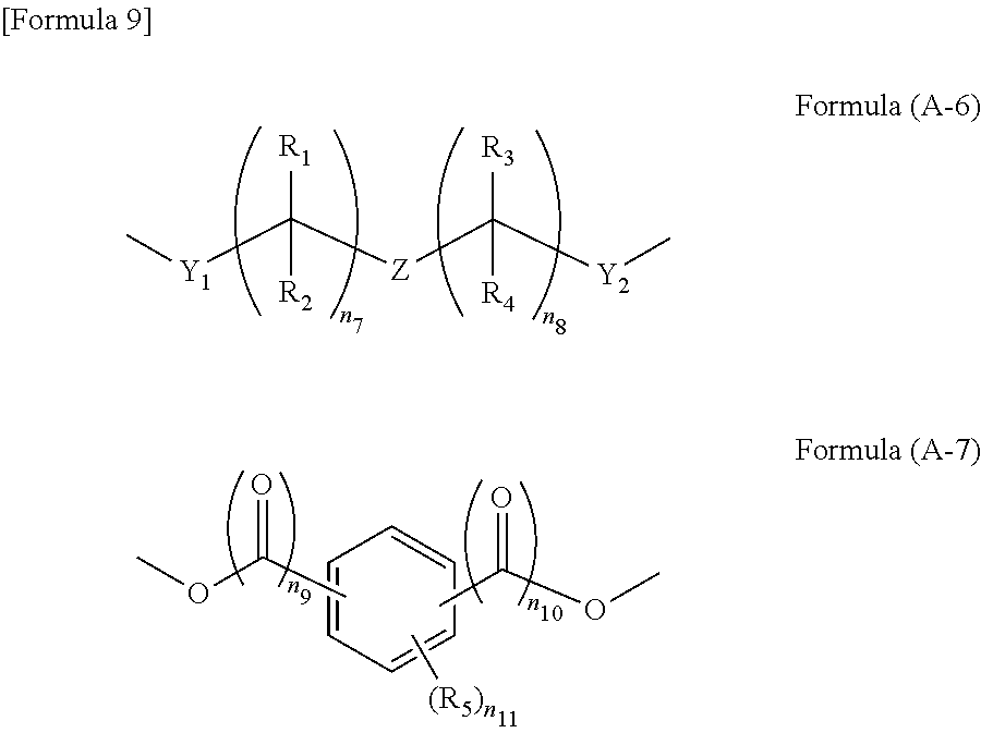
- T is preferably represented by the following formula (A-6) or the following formula (A-7).
- R 1 , R 2 , R 3 , R 4 and R 8 each independently represent a hydrogen atom, an alkyl group having 1 to 6 carbon atoms optionally substituted, an alkenyl group having 2 to 6 carbon atoms, a hydroxy group, an alkoxy group having 1 to 6 carbon atoms, a cyano group or a halogen atom, and R 2 and R 4 optionally bonded to each other to form a ring;
- —Y 1 — and —Y 2 — each independently represent —O—, —S— or —COO—;
- —Z— represents a direct bond or a divalent organic group, and preferred divalent organic group represents —O—, —S—, —S—S—, —CR 10 ⁇ CR 11 —, —C( ⁇ CR 12 R 13 )— or —C ⁇ C—;
- R 10 , R 11 , R 12 and R 13 each independently represent a hydrogen atom or
- the alkyl group having 1 to 6 carbon atoms includes the above-mentioned alkyl groups.
- the above-mentioned “optionally substituted” means that a part or all of the hydrogen atoms of the above-mentioned alkyl group may be substituted with, for example, a hydroxy group, a halogen atom, a carboxyl group, a nitro group, a cyano group, a methylenedioxy group, an acetoxy group, a methylthio group, an amino group or an alkoxy group having 1 to 9 carbon atoms.
- the above-mentioned halogen atom includes a fluorine atom, a chlorine atom, a bromine atom and an iodine atom.
- the above-mentioned alkenyl group having 2 to 6 carbon atoms includes an ethenyl group, a 1-propenyl group, a 2-propenyl group, a 1-methyl-1-ethenyl group, a 1-butenyl group, a 2-butenyl group, a 3-butenyl group, a 2-methyl-1-propenyl group, a 2-methyl-2-propenyl group, a 1-ethylethenyl group, a 1-methyl-1-propenyl group, a 1-methyl-2-propenyl group, a 1-pentenyl group, a 2-pentenyl group, a 3-pentenyl group, a 4-pentenyl group, a 1-n-propylethenyl group, a 1-methyl-1-butenyl group, a 1-methyl-2-butenyl group, a 1-methyl-3-butenyl group, a 2-ethyl-2-propenyl group, a 2-methyl-1-
- the above-mentioned alkoxy group having 1 to 6 carbon atoms includes a methoxy group, an ethoxy group, an n-propoxy group, an i-propoxy group, an n-butoxy group, an i-butoxy group, an s-butoxy group, an t-butoxy group, an n-pentyloxy group, a 1-methyl-n-butoxy group, a 2-methyl-n-butoxy group, a 3-methyl-n-butoxy group, a 1,1-dimethyl-n-propoxy group, a 1,2-dimethyl-n-propoxy group, a 2,2-dimethyl-n-propoxy group, a 1-ethyl-n-propoxy group, an n-hexyloxy group, a 1-methyl-n-pentyloxy group, a 2-methyl-n-pentyloxy group, a 3-methyl-n-pentyloxy group, a 4-methyl-n-pentyloxy group, a 1,1
- R 2 and R 4 optionally bonded to each other to form a ring means that R 2 and R 4 may be bonded to each other to form, for example, a hydrocarbon ring having 3 to 12 carbon atoms.
- the divalent organic group represented by Z is preferably represented by the following formula (A-8).
- —V 1 — represents —O—, —S—, —S—S—, —CR 10 ⁇ CR 11 —, —C( ⁇ CR 12 R 13 )— or —C ⁇ C—
- R 10 , R 11 , R 12 and Ria each independently represent a hydrogen atom or a methyl group
- —V 2 — represents —O— or —S—
- R 8 and R 9 each represent a hydrogen atom, an alkyl group having 1 to 6 carbon atoms optionally substituted, an alkenyl group having 2 to 6 carbon atoms, a hydroxy group, an alkoxy group having 1 to 6 carbon atoms, a cyano group or a halogen atom
- n 12 represents an integer of 1 to 3
- n 13 represents an integer of 0 to 2.
- alkyl group having 1 to 6 carbon atoms optionally substituted the alkenyl group having 2 to 6 carbon atoms and the alkoxy group having 1 to 6 carbon atoms are as mentioned above.
- T is preferably represented by the following formula (A-6).
- the divalent organic group represented by Z is preferably represented by the following formula (A-8).
- —Y 1 — and —Y 2 — in the above-mentioned formula (A-6) are preferably —COO—.
- the —COO— represents an ester bond. It is preferred that the carbonyl group of the ester bond is present at the position close to the unit structure containing the substituents R 1 and R 2 of formula (A-6) or to the unit structure containing the substituents R 3 and R 4 .
- the above-mentioned unit structure of the ring-opening polymerization product (C) may be exemplified, for example, as follows.
- the above-mentioned diepoxy compound (A) includes an aryl diglycidyl ether compound and an aryl diglycidyl ester compound.
- the phenyl diglycidyl ether compound or phenyl diglycidyl ester compound having the structural unit of formula (A-3) may be exemplified, for example, as follows.
- the compound represented by formula (D-1) is available as a product name: Denacol EX-711 from Nagase ChemteX Corporation.
- the compound represented by formula (D-8) is available as a product name: Denacol EX-721 from Nagase ChemteX Corporation.
- the compound represented by formula (D-13) is available as product names: Denacol EX-201 or Denacol EX-201-IM from Nagase ChemteX Corporation.
- naphthyl diglycidyl ether compound or naphthyl diglycidyl ester compound having the structural unit of formula (A-4) may be exemplified, for example, as follows.
- biphenyl diglycidyl ether compound bisphenol diglycidyl ether compound, biphenyl diglycidyl ester compound or bisphenol diglycidyl ester compound having the structural unit of formula (A-5) may be exemplified, for example, as follows.
- the “functional” referred to in the above-mentioned bi- or higher functional proton-generating compound (B) is a concept focusing on the chemical properties and chemical reactivity of a substance.
- a functional group When a functional group is referred to, the physical properties and chemical reactivity inherent to a certain compound are reminded; however, in the present application, it refers to a reactive substituent that can be bonded to another compound by generating a proton. That is, for example, the term “bifunctional” means that two reactive substituents are possessed by the above-mentioned compound.
- the reactive substituent of the present application includes a hydroxy group, an epoxy group, an acyl group, an acetyl group, a formyl group, a benzoyl group, a carboxy group, a carbonyl group, an amino group, an imino group, a cyano group, an azo group, an azi group, a thiol group, a sulfo group and an allyl group.
- the proton generating compound (B) of the present application is not particularly limited as long as it is bifunctional or higher, and preferably tetrafunctional or lower, preferably trifunctional or lower and most preferably bifunctional.
- the bi- or higher functional proton-generating compound (B) of the present application includes, for example, a compound containing two or more carboxy groups, a compound containing two or more hydroxyl groups and a compound containing two or more thiol groups.
- One or two or more species of the above-mentioned functional group may be present in the compound.
- the carboxy group-containing compound, hydroxyl group-containing compound and thiol group-containing compound having the structural unit of the above-mentioned formula (A-6) include, for example, the following.
- the weight average molecular weight of the polymerization product of the present application is within the range of preferably 500 to 10,000, and further preferably 700 to 5,000.
- the protective film-forming composition of the present invention may be prepared by dissolving each of the above-mentioned components in an organic solvent, and may be used in a uniform solution state.
- any solvents capable of dissolving the above-mentioned ring-opening polymerization product (C) may be used without any particular limitation.
- the protective film-forming composition according to the present invention is used in a uniform solution state, it is recommended to use a solvent usually used in the lithography process in combination in view of its application performance.
- organic solvents include, for example, ethylene glycol monomethyl ether, ethylene glycol monoethyl ether, methyl cellosolve acetate, ethyl cellosolve acetate, diethylene glycol monomethyl ether, diethylene glycol monoethyl ether, propylene glycol, propylene glycol monomethyl ether, propylene glycol monoethyl ether, propylene glycol monomethyl ether acetate, propylene glycol propyl ether acetate, toluene, xylene, methyl ethyl ketone, methyl isobutyl ketone, cyclopentanone, cyclohexanone, cycloheptanone, 4-methyl-2-pentanol, methyl 2-hydroxyisobutyrate, ethyl 2-hydroxyisobutyrate, ethyl ethoxyacetate, 2-hydroxyethyl acetate, methyl 3-methoxypropionat
- propylene glycol monomethyl ether propylene glycol monomethyl ether acetate, ethyl lactate, butyl lactate, cyclohexanone and the like are preferable.
- propylene glycol monomethyl ether and propylene glycol monomethyl ether acetate are preferable.
- the protective film-forming composition of the present invention may contain a cross-linking catalyst as an optional component to promote the cross-linking reaction.
- a cross-linking catalyst in addition to the acidic compound, a compound that generates an acid or a base by heat may be used.
- a sulfonic acid compound or a carboxylic acid compound may be used, and as the compound that generates an acid by heat, a thermal acid generator may be used.
- the sulfonic acid compound or the carboxylic acid compound includes, for example, p-toluenesulfonic acid, trifluoromethanesulfonic acid, pyridinium trifluoromethanesulfonate, pyridinium-p-toluenesulfonate, pyridinium-4-hydroxybenzenesulfonate, salicylic acid, camphor sulfonic acid, 5-sulfosalicyclic acid, 4-chlorobenzenesulfonic acid, 4-hydroxybenzenesulfonic acid, pyridinium-4-hydroxybenzenesulfonic acid, benzenedisulfonic acid, 1-naphthalenesulfonic acid, 4-nitrobenzenesulfonic acid, citric acid, benzoic acid and hydroxybenzoic acid.
- the thermal acid generator includes, for example, K-PURE [Registered Trademark] CXC-1612, ditto CXC-1614, ditto TAG-2172, ditto TAG-2179, ditto TAG-2678 and ditto TAG2689 (all available from King Industries, Inc.), and SI-45, SI-60, SI-80, SI-100, SI-110 and SI-150 (all available from SANSHIN CHEMICAL INDUSTRY CO., LTD.).
- K-PURE Registered Trademark
- an amine compound or an ammonium hydroxide compound may be used, and as the compound that generates a base by heat, urea may be used.
- the amine compound includes, for example, tertiary amines such as triethanolamine, tributanolamine, trimethylamine, triethylamine, tri-normal-propylamine, triisopropylamine, tri-normal-butylamine, tri-tert-butylamine, tri-normal-octylamine, triisopropanolamine, phenyldiethanolamine, stearyl diethanolamine, diazabicyclooctane, etc., and aromatic amines such as pyridine, 4-dimethylamino-pyridine, etc.
- tertiary amines such as triethanolamine, tributanolamine, trimethylamine, triethylamine, tri-normal-propylamine, triisopropylamine, tri-normal-butylamine, tri-tert-butylamine, tri-normal-octylamine, triisopropanolamine, phenyldiethanolamine,
- amine compound in addition, it includes primary amines such as benzylamine, normal-butylamine, etc., and secondary amines such as diethylamine, di-normal-butylamine, etc. as the amine compound.
- primary amines such as benzylamine, normal-butylamine, etc.
- secondary amines such as diethylamine, di-normal-butylamine, etc.
- amine compounds may be used alone or in combination of two or more.
- the ammonium hydroxide compound includes, for example, tetramethylammonium hydroxide, tetraethylammonium hydroxide, tetrapropyl-ammonium hydroxide, tetrabutylammonium hydroxide, benzyltrimethylammonium hydroxide, benzyltriethylammonium hydroxide, cetyltrimethylammonium hydroxide, phenyltrimethylammonium hydroxide and phenyltriethylammonium hydroxide.
- a compound having a thermolabile group such as an amide group, a urethane group or an aziridine group, which generates an amine by heating may be used as the compound that generates a base by heat, for example.
- the compound that generates a base by heat includes urea, benzyltrimethylammonium chloride, benzyltriethylammonium chloride, benzyldimethylphenylammonium chloride, benzyldodecyldimethylammonium chloride, benzyltributylammonium chloride and choline chloride.
- cross-linking catalysts may be used alone or in combination of two or more.
- the above-mentioned protective film-forming composition contains the cross-linking catalyst, its content is within the range of 0.0001 to 20% by weight, preferably 0.01 to 15% by weight, and further preferably 0.1 to 10% by mass, based on the total solid content of the protective film-forming composition.
- the resist underlayer film forming composition of the present invention may contain a cross-linking agent component.
- the cross-linking agent includes a melamine-based, substituted urea-based or polymer-based cross-linking agent, etc. It is preferably a cross-linking agent having at least two cross-linking formable substituents, and it is a compound such as methoxymethylated glycol uril, butoxymethylated glycol uril, methoxymethylated melamine, butoxymethylated melamine, methoxymethylated benzoguanamine, butoxymethylated benzoguanamine, methoxymethylated urea, butoxymethylated urea, methoxymethylated thiourea, methoxymethylated thiourea, or the like.
- a condensed product of these compounds may be used.
- a cross-linking agent having high heat resistance may be used.
- a compound containing a cross-linking formable substituent having an aromatic ring (for example, benzene ring, naphthalene ring) in the molecule may be used.
- Such a compound includes a compound having a partial structure of the following formula (5-1) and a polymer or oligomer having a recurring unit of the following formula (5-2).
- R 11 , R 12 , R 13 and R 14 are each a hydrogen atom or an alkyl group having 1 to 10 carbon atoms, and these alkyl groups may be referred to the above-mentioned exemplification.
- m1 meets 1 ⁇ m1 ⁇ 6 ⁇ m2
- m2 meets 1 ⁇ m2 ⁇ 5
- m3 meets 1 ⁇ m3 ⁇ 4 ⁇ m2
- m4 meets 1 ⁇ m4 ⁇ 3.
- Examples of the compound, polymer or oligomer of formula (5-1) and formula (5-2) are as follows.
- the above-mentioned compounds are commercially available as products from ASAHI YUKIZAI CORPORATION or Honshu Chemical Industry Co., Ltd.
- the compound of formula (6-22) is available as product name: TMOM-BP from ASAHI YUKIZAI CORPORATION.
- cross-linking agents may be used alone or in combination of two or more.
- the amount of the cross-linking agent to be added may vary depending on a coating solvent to be used, a base substrate to be used, a solution viscosity to be required, a film shape to be required, or the like, and it is within the range of 0.001 to 80% by weight, preferably 0.01 to 50% by weight, and further preferably 0.1 to 40% by weight based on the total solid content of the protective film-forming composition.
- these cross-linking agents may sometimes cause a cross-linking reaction due to self-condensation, they can cause a cross-linking reaction with cross-linkable substituents, when the cross-linkable substituents are present in the above-mentioned polymer of the present invention.
- the protective film-forming composition of the present invention may contain a surfactant as an optional component to improve its applicability to the semiconductor substrate.
- the above-mentioned surfactants includes, for example, nonionic surfactants including polyoxyethylene alkyl ethers such as polyoxyethylene lauryl ether, polyoxyethylene stearyl ether, polyoxyethylene cetyl ether, polyoxyethylene oleyl ether, etc., polyoxyethylene alkyl aryl ethers such as polyoxyethylene octylphenyl ether, polyoxyethylene nonyl phenyl ether, etc., sorbitan fatty acid esters such as polyoxyethylene-polyoxypropylene block copolymers, sorbitan monolaurate, sorbitan monopalmitate, sorbitan monostearate, sorbitan monooleate, sorbitan trioleate, sorbitan tristearate, etc., polyoxyethylene sorbitan fatty acid esters such as polyoxyethylene sorb
- surfactants may be used alone or in combination of two or more.
- the content thereof is within the range of 0.0001 to 10% by weight, preferably 0.01 to 5% by weight based on the total solid content of the protective film-forming composition.
- a light absorbing agent a rheology adjusting agent, an adhesive auxiliary agent, etc.
- the rheology adjusting agent is effective in improving fluidity of the protective film-forming composition.
- the adhesive auxiliary agent is effective in improving adhesion between the underlayer film and the semiconductor substrate or resist.
- the light absorbing agent that may suitably be used includes, for example, the commercially available light absorbing agents described in “Technology and Market of Industrial Dyes” (CMC Publishing Co., Ltd.) or “Dye Handbook” (edited by The Society of Organic Synthetic Chemistry, Japan), such as C.I. Disperse Yellow 1, 3, 4, 5, 7, 8, 13, 23, 31, 49, 50, 51, 54, 60, 64, 66, 68, 79, 82, 88, 90, 93, 102, 114 and 124; C.I. Disperse Orangel, 5, 13, 25, 29, 30, 31, 44, 57, 72 and 73; C.I.
- the above-mentioned light absorbing agent is usually formulated in a proportion of 10% by mass or less, and preferably 5% by mass or less based on the total solid content of the protective film-forming composition.
- the rheology adjusting agent is added for the purpose of mainly improving fluidity of the protective film-forming composition, and particularly in the baking process, improving uniformity of the film thickness of the resist underlayer film or heightening filling property of the protective film-forming composition inside the hole.
- phthalic acid derivatives such as dimethyl phthalate, diethyl phthalate, diisobutyl phthalate, dihexyl phthalate, butylisodecyl phthalate, etc.
- adipic acid derivatives such as di-normal-butyl adipate, diisobutyl adipate, diisooctyl adipate, octyldecyl adipate, etc.
- maleic acid derivatives such as di-normal-butylmaleate, diethyl maleate, dinonyl maleate, etc.
- oleic acid derivatives such as methyl oleate, butyl oleate, tetrahydrofurfuryl oleate, etc.
- stearic acid derivatives such as normal-butyl stearate, glyceryl stearate, etc.
- These rheology adjusting agents are usually formulated in a proportion of less than 30% by
- the adhesive auxiliary agent is added for the purpose of mainly improving adhesiveness between the protective film-forming composition and the substrate or resist, and particularly preventing the resist from peeling off during development.
- Specific examples thereof include chlorosilanes such as trimethylchlorosilane, dimethylmethylol chlorosilane, methyldiphenylchlorosilane, chloromethyldimethylchlorosilane, etc., alkoxysilanes such as trimethylmethoxysilane, dimethyldiethoxysilane, methyldimethoxysilane, dimethylmethylol ethoxysilane, diphenyldimethoxysilane, phenyltriethoxysilane, etc., silazanes such as hexamethyl-disilazane, N,N′-bis(trimethylsilyl)urea, dimethyltrimethylsilylamine, trimethyl-silylimidazole, etc., silanes such as methylol trichloro
- a solid content of the protective film-forming composition according to the present invention is usually made 0.1 to 70% by mass, and preferably 0.1 to 60% by mass.
- the solid content is the content ratio of all the components excluding the solvent from the protective film-forming composition.
- the proportion of the ring-opening polymerized product in the solid content is within the range of 1 to 100% by mass, 1 to 99.9% by mass, 50 to 99.9% by mass, 50 to 95% by mass, and 50 to 90% by mass by increasing preference.
- the substrate equipped with a resist pattern according to the present invention may be produced by applying the above-mentioned protective film-forming composition onto a semiconductor substrate and baking the applied composition.
- the semiconductor substrate to which the protective film-forming composition of the present invention is applied includes, for example, silicon wafers, germanium wafers, and compound semiconductor wafers such as gallium arsenide, indium phosphate, gallium nitride, indium nitride, aluminum nitride, etc.
- the inorganic film may be formed by, for example, ALD (atomic layer deposition) method, CVD (chemical vapor deposition) method, reactive sputtering method, ion plating method, vacuum deposition method, or spin coating method (spin-on-glass: SOG).
- ALD atomic layer deposition
- CVD chemical vapor deposition
- reactive sputtering method reactive sputtering method
- ion plating method vacuum deposition method
- spin coating method spin-on-glass: SOG
- the inorganic film includes, for example, a polysilicon film, a silicon oxide film, a silicon nitride film, a BPSG (Boro-Phospho Silicate Glass) film, a titanium nitride film, a titanium oxynitride film, a tungsten nitride film, a gallium nitride film and a gallium arsenide film.
- a polysilicon film for example, a polysilicon film, a silicon oxide film, a silicon nitride film, a BPSG (Boro-Phospho Silicate Glass) film, a titanium nitride film, a titanium oxynitride film, a tungsten nitride film, a gallium nitride film and a gallium arsenide film.
- the protective film-forming composition of the present invention is applied by a suitable application method such as a spinner, a coater, etc. Thereafter, by baking the applied composition using a heating means such as a hot plate, etc., a protective film is formed.
- a suitable application method such as a spinner, a coater, etc.
- a heating means such as a hot plate, etc.
- a protective film is formed.
- the baking conditions these are appropriately selected from a baking temperature of 100° C. to 400° C. and a baking time of 0.3 minute to 60 minutes. These are preferably a baking temperature of 120° C. to 350° C. and a baking time of 0.5 minute to 30 minutes, and more preferably a baking temperature of 150° C. to 300° C. and a baking time of 0.8 minute to 10 minutes.
- the film thickness of the protective film to be formed is within the range of 0.001 ⁇ m to 10 ⁇ m, preferably 0.002 ⁇ m to 1 ⁇ m, and more preferably 0.005 ⁇ m to 0.5 ⁇ m. If the temperature at the time of baking is lower than the above-mentioned range, cross-linking sometimes becomes insufficient so that a resistance of the formed protective film to a resist solvent or a basic aqueous hydrogen peroxide solution is sometimes difficultly obtained. On the other hand, if the temperature at the time of baking is higher than the above-mentioned range, the protective film is sometimes decomposed by heat.
- the exposure is carried out through a mask (reticle) for forming a predetermined pattern, and for example, i-line, KrF excimer laser, ArF excimer laser, EUV (extreme ultraviolet) or EB (electron beam) is used.
- a mask reticle
- i-line KrF excimer laser, ArF excimer laser, EUV (extreme ultraviolet) or EB (electron beam)
- EUV extreme ultraviolet
- EB electrotron beam
- the alkaline developer that may be used includes, for example, an aqueous solution of alkalis including inorganic alkalis such as sodium hydroxide, potassium hydroxide, sodium carbonate, sodium silicate, sodium metasilicate, aqueous ammonia, etc., primary amines such as ethylamine, n-propylamine, etc., secondary amines such as diethylamine, di-n-butylamine, etc., tertiary amines such as triethylamine, methyl-diethylamine, etc., alcohol amines such as dimethylethanolamine, triethanolamine, etc., quaternary ammonium salts such as tetramethylammonium hydroxide, tetraethylammonium hydroxide, choline, etc., cyclic amines such as pyrrole, piperidine, etc.
- inorganic alkalis such as sodium hydroxide, potassium hydroxide, sodium carbonate, sodium silicate
- aqueous solution of the alkalis by adding an appropriate amount of an alcohol such as isopropyl alcohol, etc., a surfactant such as nonionic, etc.
- a preferable developer is a quaternary ammonium salt, and more preferably tetramethylammonium hydroxide and choline.
- a surfactant, etc. it is possible to add a surfactant, etc., to these developers. It is also possible to use a method including the step of developing the portion in which an alkali dissolution rate of the photoresist has not been improved, while using an organic solvent such as butyl acetate, etc. in place of the alkaline developer.
- the protective film is subjected to dry etching. At that time, the surface of inorganic film is allowed to expose if the inorganic film has been formed on the surface of the semiconductor substrate used, and the surface of semiconductor substrate is allowed to expose if no inorganic film has been formed on the surface of the semiconductor substrate used.
- wet etching is carried out using a wet etching liquid for semiconductors to form a desired pattern.
- the wet etching liquid for semiconductor a chemical solution usually used for etching processing of a wafer for semiconductor may be used, and for example, both of a substance showing acidity and a substance showing basicity may be used.
- the substance showing acidity includes, for example, hydrogen peroxide, hydrofluoric acid, ammonium fluoride, acidic ammonium fluoride, ammonium hydrogen fluoride, buffered hydrofluoric acid, hydrochloric acid, nitric acid, sulfuric acid, phosphoric acid or a mixed liquid of these.
- Specific examples thereof include SC-2 (hydrochloric acid-hydrogen peroxide solution).
- the substance showing basicity includes basic aqueous hydrogen peroxide solution, in which a hydrogen peroxide solution is mixed with an organic amine such as ammonia, sodium hydroxide, potassium hydroxide, sodium cyanide, potassium cyanide, triethanolamine, etc., so as to make the pH of the resulting solution is basic.
- an organic amine such as ammonia, sodium hydroxide, potassium hydroxide, sodium cyanide, potassium cyanide, triethanolamine, etc.
- SC-1 ammonia-hydrogen peroxide solution
- any chemical liquid that can be basic pH may also be used as a chemical liquid for wet etching, such as a mixture of urea and a hydrogen peroxide solution, in which the thermal decomposition of urea generates ammonia, which in turn would ultimately make the mixture basic pH.
- an acidic aqueous hydrogen peroxide or a basic aqueous hydrogen peroxide solution is preferable.
- These chemical liquids may contain an additive such as a surfactant, etc.
- An operating temperature of the wet etching liquid for semiconductor is desirably 25° C. to 90° C., and more desirably 40° C. to 80° C.
- As a wet etching time it is desirable to be 0.5 min to 30 min, and further desirably 1 min to 20 min.
- the device etc. used for determining the weight average molecular weight of the polymers obtained in Synthetic Examples below are shown as follows.
- Device HLC-8320GPC manufactured by TOSOH CORPORATION GPC column: Shodex [registered trademark] ⁇ Asahipak [registered trademark] (SHOWADENKO K. K.)
- the obtained reaction product corresponded to formula (B-1).
- the weight average molecular weight Mw determined by GPC in terms of polystyrene was 3,200.
- the obtained reaction product corresponded to formula (B-2).
- the weight average molecular weight Mw determined by GPC in terms of polystyrene was 2,700.
- the obtained reaction product corresponded to formula (B-3).
- the weight average molecular weight Mw determined by GPC in terms of polystyrene was 2,600.
- the obtained reaction product corresponded to formula (B-4).
- the weight average molecular weight Mw determined by GPC in terms of polystyrene was 3,100.
- the obtained reaction product corresponded to formula (B-5).
- the weight average molecular weight Mw determined by GPC in terms of polystyrene was 2,000.
- the obtained reaction product corresponded to formula (B-6).
- the weight average molecular weight Mw determined by GPC in terms of polystyrene was 2,600.
- the obtained reaction product corresponded to formula (B-7).
- the weight average molecular weight Mw determined by GPC in terms of polystyrene was 1,900.
- the obtained reaction product corresponded to formula (B-8).
- the weight average molecular weight Mw determined by GPC in terms of polystyrene was 1,500.
- the obtained reaction product corresponded to formula (B-9).
- the weight average molecular weight Mw determined by GPC in terms of polystyrene was 3,500.
- reaction flask containing 10.00 g of resorcinol diglycidyl ether product name: Denacol EX-201-IM, available from Nagase ChemteX Corporation
- 6.09 g of succinic acid, 0.80 g of ethyltriphenylphosphonium bromide and 67.55 g of propylene glycol monomethyl ether was heated while stirring at 100° C. for 27 hours.
- the obtained reaction product corresponded to formula (B-10).
- the weight average molecular weight Mw determined by GPC in terms of polystyrene was 3,000.
- reaction flask containing 10.00 g of resorcinol diglycidyl ether product name: Denacol EX-201-IM, available from Nagase ChemteX Corporation
- 6.71 g of itaconic acid 0.80 g of ethyltriphenylphosphonium bromide, 0.03 g of hydroquinone and 70.03 g of propylene glycol monomethyl ether was heated while stirring at 100° C. for 25 hours.
- the obtained reaction product corresponded to formula (B-11).
- the weight average molecular weight Mw determined by GPC in terms of polystyrene was 1,700.
- reaction flask containing 10.00 g of resorcinol diglycidyl ether product name: Denacol EX-201-IM, available from Nagase ChemteX Corporation
- 5.99 g of fumaric acid 0.80 g of ethyltriphenylphosphonium bromide, 0.03 g of hydroquinone and 67.14 g of propylene glycol monomethyl ether was heated while stirring at 100° C. for 26 hours.
- the obtained reaction product corresponded to formula (B-12).
- the weight average molecular weight Mw determined by GPC in terms of polystyrene was 4,500.
- the obtained reaction product corresponded to formula (C-1).
- the weight average molecular weight Mw determined by GPC in terms of polystyrene was 2,800.
- the obtained reaction product corresponded to formula (C-2).
- the weight average molecular weight Mw determined by GPC in terms of polystyrene was 1,900.
- the obtained reaction product corresponded to formula (C-3).
- the weight average molecular weight Mw determined by GPC in terms of polystyrene was 4,400.
- Each of the protective film-forming compositions prepared in Examples 1 to 12 and Comparative Examples 1 to 5 was applied (spin-coat) on a silicon wafer by a spin coater.
- the composition-applied silicon wafer was heated on a hot plate at 250° C. for 1 minute to form an applied film (protective film) having a film thickness of 100 nm.
- the silicon wafer carrying the protective film thereon was immersed in a mixed solvent of propylene glycol monomethyl ether and propylene glycol monomethyl ether acetate having a weight-basis mixing ratio of 7:3 for 1 minute. After the immersion, the wafer was spin-dried and baked at 100° C. for 30 seconds.
- the film thicknesses of the protective film before and after the immersion in the mixed solvent were measured by an optical interference film thickness meter (product name: NanoSpec 6100, manufactured by Nanometrics Japan Ltd.).
- the evaluation of the resist solvent resistance was carried out by calculating the percent film thickness reduction rate of the protective film removed by the immersion in the solvent according to the calculation formula: ((film thickness before immersion in solvent) ⁇ (film thickness after immersion in solvent)) ⁇ (film thickness before immersion in solvent) ⁇ 100; and evaluating the calculated percent film thickness reduction rate.
- the results are shown in Table 1. Incidentally, if the film thickness reduction rate is about 1% or less, it can be said that the film has a sufficient resist solvent resistance.
- the protective film-forming compositions of Examples 1 to 12 and Comparative Examples 1 to 5 had an extremely small change in film thickness even after being immersed in the resist solvent. Accordingly, the protective film-forming compositions of Examples 1 to 12 have a sufficient resist solvent resistance to function as a protective film.
- each of the protective film-forming compositions prepared in Examples 1 to 12 and Comparative Examples 1 to 5 was applied onto a TiN-deposited substrate having a deposit film thickness of 50 nm, and heated at 250° C. for 1 minute to form a protective film so as to have a film thickness of 100 nm.
- 28% aqueous ammonia, 33% hydrogen peroxide and water were mixed in a weight-basis mixing ratio of 1:1:2, respectively, to prepare a basic aqueous hydrogen peroxide solution.
- the TiN-deposited substrate carrying the protective film-forming composition applied thereon was immersed into the basic aqueous hydrogen peroxide solution heated at 50° C., and the period (peeling time) from the time of immediately after the immersion to the time of peeling off of the protective film from the substrate was measured.
- the results of the resistance test to the basic aqueous hydrogen peroxide solution are shown in Table 2. Incidentally, it can be said that the longer the peeling time, the higher the resistance to the wet etching liquid using the basic aqueous hydrogen peroxide solution.
- each of the protective film-forming compositions prepared in Examples 1 to 12 and Comparative Examples 1 to 5 was applied onto a TiN-deposited substrate having a deposit film thickness of 50 nm, and heated at 250° C. for 1 minute to form a protective film so as to have a film thickness of 100 nm.
- 85% phosphoric acid and water were mixed in a weight-basis mixing ratio of 1:1 to prepare an acidic aqueous hydrogen peroxide solution.
- the TiN-deposited substrate carrying the protective film-forming composition applied thereon was immersed into the acidic aqueous hydrogen peroxide solution heated at 60° C., and the period (peeling time) from the time of immediately after the immersion to the time of the peeling off of the protective film from the substrate was measured.
- the results of the resistance test to the acidic aqueous hydrogen peroxide solution are shown in Table 2. Incidentally, it can be said that the longer the peeling time, the higher the resistance to the wet etching liquid using the acidic aqueous hydrogen peroxide solution.
- Examples 1 to 5 and Examples 7 to 12 had a longer peeling time of the protective film to the basic hydrogen peroxide solution than Comparative Examples 1 to 3. That is, Examples 1 to 5 and Examples 7 to 12 have a good resistance to the wet etching liquid using the basic hydrogen peroxide solution than Comparative Examples 1 to 3.
- Examples 2 to 12 had a longer peeling time of the protective film to the acidic aqueous hydrogen peroxide solution than Comparative Examples 1 to 3. That is, Examples 2 to 12 have a good chemical liquid resistance to the acidic aqueous hydrogen peroxide solution than Comparative Examples 1 to 3, and they have a resistance to the wet etching liquid using the acidic aqueous hydrogen peroxide solution.
- Examples 1 to 12 show a good chemical liquid resistance to the basic hydrogen peroxide solution or the acidic aqueous hydrogen peroxide solution or both of them than Comparative Examples 1 to 3, so that the composition of Examples 1 to 12 are useful as the protective film to the wet etching liquid for semiconductors.
- each of the protective film-forming compositions prepared in the above Examples 1 to 12 and Comparative Examples 4 to 5 was applied onto a silicon wafer and heated at 250° C. for 1 minute to form a protective film so as to have a film thickness of 100 nm.
- the formed protective film and the resist underlayer film (product name: ARC (Registered Trademark) 29A, available from Nissan Chemical Corporation) for semiconductor lithography were subjected to dry etching with a nitrogen gas using a dry etching device (product name: RIE-10NR, manufactured by SUMCO CORPORATION) to determine the ratio of the dry etching rate (selection ratio of dry etching rate) of the protective film based on that of the resist underlayer film.
- the results of measurement of the etching selection ratio are shown in Table 3. Incidentally, it can be said that the larger the etching selection ratio, the faster the dry etching rate.
- each of the protective film-forming compositions prepared in Examples 1 to 12 and Comparative Examples 4 to 5 was applied onto a TiN-deposited, silicon substrate having a deposit film thickness of 5 nm and having a depth of 200 nm and a trench width of 50 nm. The resultant substrate was then heated at 250° C. for 1 minute.
- the protective film-forming composition was prepared so as to provide a film thickness of 100 nm after heated on the silicon wafer at 250° C. for 1 minute.
- the film thickness at a dense pattern area with a pitch of 100 nm and that at an open area having no pattern formed were observed by using a scanning electron microscope (product name: S-4800, manufactured by Hitachi High-Technologies Corporation), and the difference (film thickness bias) of the film thicknesses between the dense and the open area was determined.
- the results of determining the film thickness bias are shown in Table 3. Incidentally, it can be said that the smaller the film thickness bias, the smaller the difference in the film thicknesses between the dense area and the open area, so that the composition can be more flatly applied on a base substrate having a pattern.
- Examples 1 to 12 have a higher dry etching selection ratio than Comparative Examples 4 to 5, so that the composition of Examples 1 to 12 have a rapid dry etching rate. That is, Examples 1 to 12 may shorten the dry etching time necessary for removing the protective film, and reduce damage to the base substrate, so that the compositions of Examples 1 to 12 are useful.
- Example 1 to 12 the difference in film thicknesses (film thickness bias) between the dense area and the open area is smaller than in Comparative Examples 4 to 5, so that it can be said that the compositions of Examples 1 to 12 can be more flatly applied on a base substrate having a pattern. That is, Examples 1 to 12 are unlikely to cause unevenness of the film thickness on a base substrate having a pattern, and permit uniform removal of a certain amount of the protective film in a desired etching time, so that the compositions of Examples 1 to 12 are useful.
- Example 1 to Example 12 are excellent in resistance to a wet etching liquid for semiconductors using a basic aqueous hydrogen peroxide solution or an acidic aqueous hydrogen peroxide solution than Comparative Examples 1 to 3, and are rapid in etching rate than Comparative Examples 4 to 5, so that the compositions of Examples 1 to 12 can be flatly applied on a base substrate having a pattern. Therefore, according to the present invention, there is provided a protective film-forming composition having a high wet etching resistance, high etching rate, and high flatness in combination.
- the protective film-forming composition according to the present invention is excellent in resistance to wet etching liquids applied for processing a substrate, and has a high dry etching rate, so that the composition permits easy processing of a substrate; and the composition provides a protective film excellent in flatness, when it is applied to a stepped substrate.
Landscapes
- Chemical & Material Sciences (AREA)
- Chemical Kinetics & Catalysis (AREA)
- General Physics & Mathematics (AREA)
- Physics & Mathematics (AREA)
- Medicinal Chemistry (AREA)
- Organic Chemistry (AREA)
- Polymers & Plastics (AREA)
- Health & Medical Sciences (AREA)
- Structural Engineering (AREA)
- Architecture (AREA)
- Engineering & Computer Science (AREA)
- Materials For Photolithography (AREA)
- General Chemical & Material Sciences (AREA)
- Organic Low-Molecular-Weight Compounds And Preparation Thereof (AREA)
- Photosensitive Polymer And Photoresist Processing (AREA)
- Epoxy Resins (AREA)
- Exposure Of Semiconductors, Excluding Electron Or Ion Beam Exposure (AREA)
Abstract
Description
[2]
The protective film-forming composition according to [1], wherein the ring-opening polymerization product (C) is represented by a unit structure of the following formula (A-1):

wherein, in formula (A-1), Q represents a divalent organic group from the ring-opening polymerization of the diepoxy compound (A), and T represents a divalent organic group derived from the bi- or higher functional proton-generating compound (B).
[3]
The protective film-forming composition according to [2], wherein Q in formula (A-1) is represented by the following formula (A-2):

wherein, in formula (A-2), Ar represents a divalent arylene group, and n1 and n2 each independently represent an integer of 0 or 1.
[4]
The protective film-forming composition according to [3], wherein Ar in formula (A-2) is represented by any of the following formula (A-3), the following formula (A-4) and the following formula (A-5):

wherein, in formula (A-3) to formula (A-5), X1, X2, X3 and X4 each independently represent an alkyl group having 1 to 6 carbon atoms; —W— represents any of a direct bond, —CH2—, —C(CH3)2—, —C(CF3)2, —CO—, —O—, —S— or —SO2—; n3, n3 and n6 each independently represent an integer of 0 to 4; and n4 represents an integer of 0 to 6.
[5]
The protective film-forming composition according to [1], wherein T in formula (A-1) is represented by the following formula (A-6) or the following formula (A-7):

wherein, in formula (A-6) or formula (A-7), R1, R2, R3, R4 and R5 each independently represent a hydrogen atom, an alkyl group having 1 to 6 carbon atoms optionally substituted, an alkenyl group having 2 to 6 carbon atoms, a hydroxy group, an alkoxy group having 1 to 6 carbon atoms, a cyano group or a halogen atom, and R2 and R4 optionally bonded to each other to form a ring; —Y1— and —Y2— each independently represent —O—, —S—, —COO— or —COO—; Z represents a direct bond or a divalent organic group; n7 and n8 each independently represent an integer of 0 to 5; n9 and n10 each independently represent an integer of 0 or 1; and n11 represents an integer of 0 to 4.
[6]
The protective film-forming composition according to [5], wherein the divalent organic group represented by Z in formula (A-6) is represented by the following formula (A-8):

wherein, in formula (A-8), —V1— represents —O—, —S—, —S—S—, —CR10═CR11—, —C(═CR12R13)— or —C≡C—; R10, R11, R12 and R13 each independently represent a hydrogen atom or a methyl group: —V2— represents —O— or —S—; R8 and R9 each independently represent a hydrogen atom, an alkyl group having 1 to 6 carbon atoms optionally substituted, an alkenyl group having 2 to 6 carbon atoms, a hydroxy group, an alkoxy group having 1 to 6 carbon atoms, a cyano group or a halogen atom; n12 represents an integer of 1 to 3; and n13 represents an integer of 0 to 2.
[7]
The protective film-forming composition according to [4], wherein Ar in formula (A-2) is represented by formula (A-3).
[8]
The protective film-forming composition according to [7], wherein n3 in formula (A-3) is 0.
[9]
The protective film-forming composition according to [5], wherein -T- in formula (A-1) is represented by formula (A-6).
[10]
The protective film-forming composition according to [9], wherein —Y1— and —Y2— in formula (A-6) are —COO—.
[11]
The protective film-forming composition according to any one of [1] to [10], which further comprises a cross-linking catalyst.
[12]
The protective film-forming composition according to any one of [1] to [11], which further comprises a cross-linking agent.
[13]
The protective film-forming composition according to any one of [1] to [12], which further comprises a surfactant.
[14]
A protective film which comprises a baked product of an applied film comprising the protective film-forming composition according to any one of [1] to [13].
[15]
A method for producing a substrate equipped with a resist pattern characterized by being used for manufacturing a semiconductor, which comprises the steps of:

wherein, in formula (A-1), Q represents a divalent organic group from the ring-opening polymerization of the diepoxy compound (A), and T represents a divalent organic group derived from the bi- or higher functional proton-generating compound (B).

wherein, in formula (A-2), Ar represents a divalent arylene group, and n1 and n2 each independently represent an integer of 0 or 1.

wherein, in formula (A-3) to formula (A-5), X1, X2, X3 and X4 each independently represent an alkyl group having 1 to 6 carbon atoms; —W— represents any of a direct bond, —CH2—, —C(CH3)2—, —C(CF3)2, —CO—, —O—, —S— or —SO2—; n3, n8 and n6 each independently represent an integer of 0 to 4; and n4 represents an integer of 0 to 6.
wherein, in formula (A-6) or formula (A-7), R1, R2, R3, R4 and R8 each independently represent a hydrogen atom, an alkyl group having 1 to 6 carbon atoms optionally substituted, an alkenyl group having 2 to 6 carbon atoms, a hydroxy group, an alkoxy group having 1 to 6 carbon atoms, a cyano group or a halogen atom, and R2 and R4 optionally bonded to each other to form a ring; —Y1— and —Y2— each independently represent —O—, —S— or —COO—; —Z— represents a direct bond or a divalent organic group, and preferred divalent organic group represents —O—, —S—, —S—S—, —CR10═CR11—, —C(═CR12R13)— or —C≡C—; R10, R11, R12 and R13 each independently represent a hydrogen atom or a methyl group; n7 and n8 each independently represent an integer of 0 to 5; n9 and n10 each independently represent an integer of 0 or 1; and n11 represents an integer of 0 to 4.

wherein, in formula (A-8), —V1— represents —O—, —S—, —S—S—, —CR10═CR11—, —C(═CR12R13)— or —C≡C—; R10, R11, R12 and Ria each independently represent a hydrogen atom or a methyl group; —V2— represents —O— or —S—; R8 and R9 each represent a hydrogen atom, an alkyl group having 1 to 6 carbon atoms optionally substituted, an alkenyl group having 2 to 6 carbon atoms, a hydroxy group, an alkoxy group having 1 to 6 carbon atoms, a cyano group or a halogen atom; n12 represents an integer of 1 to 3; and n13 represents an integer of 0 to 2.


To 4.04 g of the solution (the solid content is 16.2% by weight) of the reaction product corresponding to the above-mentioned formula (B-1) were added 0.13 g of 3,3′,5,5′-tetrakis(methoxymethyl)-4,4′-dihydroxybiphenyl (product name: TMOM-BP, available from Honshu Chemical Industry Co., Ltd.) as a cross-linking agent, 0.01 g of pyridinium-4-hydroxybenzenesulfonate as a cross-linking catalyst, 0.001 g of a fluorine-based surfactant (product name: MEGAFACE R-40, available from DIC Corporation) as a surfactant, 13.89 g of propylene glycol monomethyl ether and 1.92 g of propylene glycol monomethyl ether acetate to prepare a solution of a protective film-forming composition.

To 3.93 g of the solution (the solid content is 16.7% by weight) of the reaction product corresponding to the above-mentioned formula (B-2) were added 0.13 g of 3,3′,5,5′-tetrakis(methoxymethyl)-4,4′-dihydroxybiphenyl (product name: TMOM-BP, available from Honshu Chemical Industry Co., Ltd.) as a cross-linking agent, 0.01 g of pyridinium-4-hydroxybenzenesulfonate as a cross-linking catalyst, 0.001 g of a fluorine-based surfactant (product name: MEGAFACE R-40, available from DIC Corporation) as a surfactant, 14.00 g of propylene glycol monomethyl ether and 1.92 g of propylene glycol monomethyl ether acetate to prepare a solution of a protective film-forming composition.

To 3.79 g of the solution (the solid content is 17.3% by weight) of the reaction product corresponding to the above-mentioned formula (B-3) were added 0.13 g of 3,3′,5,5′-tetrakis(methoxymethyl)-4,4′-dihydroxybiphenyl (product name: TMOM-BP, available from Honshu Chemical Industry Co., Ltd.) as a cross-linking agent, 0.01 g of pyridinium-4-hydroxybenzenesulfonate as a cross-linking catalyst, 0.001 g of a fluorine-based surfactant (product name: MEGAFACE R-40, available from DIC Corporation) as a surfactant, 14.15 g of propylene glycol monomethyl ether and 1.92 g of propylene glycol monomethyl ether acetate to prepare a solution of a protective film-forming composition.

To 4.03 g of the solution (the solid content is 16.3% by weight) of the reaction product corresponding to the above-mentioned formula (B-4) were added 0.13 g of 3,3′,5,5′-tetrakis(methoxymethyl)-4,4′-dihydroxybiphenyl (product name: TMOM-BP, available from Honshu Chemical Industry Co., Ltd.) as a cross-linking agent, 0.01 g of pyridinium-4-hydroxybenzenesulfonate as a cross-linking catalyst, 0.001 g of a fluorine-based surfactant (product name: MEGAFACE R-40, available from DIC Corporation) as a surfactant, 13.91 g of propylene glycol monomethyl ether and 1.92 g of propylene glycol monomethyl ether acetate to prepare a solution of a protective film-forming composition.

To 3.73 g of the solution (the solid content is 17.6% by weight) of the reaction product corresponding to the above-mentioned formula (B-5) were added 0.13 g of 3,3′,5,5′-tetrakis(methoxymethyl)-4,4′-dihydroxybiphenyl (product name: TMOM-BP, available from Honshu Chemical Industry Co., Ltd.) as a cross-linking agent, 0.01 g of pyridinium-4-hydroxybenzenesulfonate as a cross-linking catalyst, 0.001 g of a fluorine-based surfactant (product name: MEGAFACE R-40, available from DIC Corporation) as a surfactant, 14.21 g of propylene glycol monomethyl ether and 1.92 g of propylene glycol monomethyl ether acetate to prepare a solution of a protective film-forming composition.

To 3.52 g of the solution (the solid content is 18.6% by weight) of the reaction product corresponding to the above-mentioned formula (B-6) were added 0.13 g of 3,3′,5,5′-tetrakis(methoxymethyl)-4,4′-dihydroxybiphenyl (product name: TMOM-BP, available from Honshu Chemical Industry Co., Ltd.) as a cross-linking agent, 0.01 g of pyridinium-4-hydroxyphenylbenzene as a cross-linking catalyst, 0.001 g of a fluorine-based surfactant (product name: MEGAFACE R-40, available from DIC Corporation) as a surfactant, 14.41 g of propylene glycol monomethyl ether and 1.92 g of propylene glycol monomethyl ether acetate to prepare a solution of a protective film-forming composition.

To 4.07 g of the solution (the solid content is 16.1% by weight) of the reaction product corresponding to the above-mentioned formula (B-7) were added 0.13 g of 3,3′,5,5′-tetrakis(methoxymethyl)-4,4′-dihydroxybiphenyl (product name: TMOM-BP, available from Honshu Chemical Industry Co., Ltd.) as a cross-linking agent, 0.01 g of pyridinium-4-hydroxybenzenesulfonate as a cross-linking catalyst, 0.001 g of a fluorine-based surfactant (product name: MEGAFACE R-40, available from DIC Corporation) as a surfactant, 13.87 g of propylene glycol monomethyl ether and 1.92 g of propylene glycol monomethyl ether acetate to prepare a solution of a protective film-forming composition.

To 3.59 g of the solution (the solid content is 18.2% by weight) of the reaction product corresponding to the above-mentioned formula (B-8) were added 0.13 g of 3,3′,5,5′-tetrakis(methoxymethyl)-4,4′-dihydroxybiphenyl (product name: TMOM-BP, available from Honshu Chemical Industry Co., Ltd.) as a cross-linking agent, 0.01 g of pyridinium-4-hydroxybenzenesulfonate as a cross-linking catalyst, 0.001 g of a fluorine-based surfactant (product name: MEGAFACE R-40, available from DIC Corporation) as a surfactant, 14.31 g of propylene glycol monomethyl ether and 1.92 g of propylene glycol monomethyl ether acetate to prepare a solution of a protective film-forming composition.

To 4.16 g of the solution (the solid content is 16.8% by weight) of the reaction product corresponding to the above-mentioned formula (B-9) were added 0.13 g of 3,3′,5,5′-tetrakis(methoxymethyl)-4,4′-dihydroxybiphenyl (product name: TMOM-BP, available from Honshu Chemical Industry Co., Ltd.) as a cross-linking agent, 0.01 g of pyridinium-4-hydroxybenzenesulfonate as a cross-linking catalyst, 0.001 g of a fluorine-based surfactant (product name: MEGAFACE R-40, available from DIC Corporation) as a surfactant, 13.78 g of propylene glycol monomethyl ether and 1.92 g of propylene glycol monomethyl ether acetate to prepare a solution of a protective film-forming composition.

To 3.93 g of the solution (the solid content is 16.7% by weight) of the reaction product corresponding to the above-mentioned formula (B-10) were added 0.13 g of 3,3′,5,5′-tetrakis(methoxymethyl)-4,4′-dihydroxybiphenyl (product name: TMOM-BP, available from Honshu Chemical Industry Co., Ltd.) as a cross-linking agent, 0.01 g of pyridinium-4-hydroxybenzenesulfonate as a cross-linking catalyst, 0.001 g of a fluorine-based surfactant (product name: MEGAFACE R-40, available from DIC Corporation) as a surfactant, 13.94 g of propylene glycol monomethyl ether and 1.92 g of propylene glycol monomethyl ether acetate to prepare a solution of a protective film-forming composition.

To 3.60 g of the solution (the solid content is 18.2% by weight) of the reaction product corresponding to the above-mentioned formula (B-11) were added 0.13 g of 3,3′,5,5′-tetrakis(methoxymethyl)-4,4′-dihydroxybiphenyl (product name: TMOM-BP, available from Honshu Chemical Industry Co., Ltd.) as a cross-linking agent, 0.01 g of pyridinium-4-hydroxybenzenesulfonate as a cross-linking catalyst, 0.001 g of a fluorine-based surfactant (product name: MEGAFACE R-40, available from DIC Corporation) as a surfactant, 14.34 g of propylene glycol monomethyl ether and 1.92 g of propylene glycol monomethyl ether acetate to prepare a solution of a protective film-forming composition.

To 3.92 g of the solution (the solid content is 16.7% by weight) of the reaction product corresponding to the above-mentioned formula (B-12) were added 0.13 g of 3,3′,5,5′-tetrakis(methoxymethyl)-4,4′-dihydroxybiphenyl (product name: TMOM-BP, available from Honshu Chemical Industry Co., Ltd.) as a cross-linking agent, 0.01 g of pyridinium-4-hydroxybenzenesulfonate as a cross-linking catalyst, 0.001 g of a fluorine-based surfactant (product name: MEGAFACE R-40, available from DIC Corporation) as a surfactant, 14.01 g of propylene glycol monomethyl ether and 1.92 g of propylene glycol monomethyl ether acetate to prepare a solution of a protective film-forming composition.

To 3.97 g of the solution (the solid content is 16.5% by weight) of the reaction product corresponding to the above-mentioned formula (C-1) were added 0.13 g of 3,3′,5,5′-tetrakis(methoxymethyl)-4,4′-dihydroxybiphenyl (product name: TMOM-BP, available from Honshu Chemical Industry Co., Ltd.) as a cross-linking agent, 0.01 g of pyridinium-4-hydroxybenzenesulfonate as a cross-linking catalyst, 0.001 g of a fluorine-based surfactant (product name: MEGAFACE R-40, available from DIC Corporation) as a surfactant, 13.96 g of propylene glycol monomethyl ether and 1.92 g of propylene glycol monomethyl ether acetate to prepare a solution of a protective film-forming composition.

To 4.08 g of the solution (the solid content is 16.1% by weight) of the reaction product corresponding to the above-mentioned formula (C-2) were added 0.13 g of 3,3′,5,5′-tetrakis(methoxymethyl)-4,4′-dihydroxybiphenyl (product name: TMOM-BP, available from Honshu Chemical Industry Co., Ltd.) as a cross-linking agent, 0.01 g of pyridinium-4-hydroxybenzenesulfonate as a cross-linking catalyst, 0.001 g of a fluorine-based surfactant (product name: MEGAFACE R-40, available from DIC Corporation) as a surfactant, 13.86 g of propylene glycol monomethyl ether and 1.92 g of propylene glycol monomethyl ether acetate to prepare a solution of a protective film-forming composition.

To 3.81 g of the solution (the solid content is 17.2% by weight) of the reaction product corresponding to the above-mentioned formula (C-3) were added 0.13 g of 3,3′,5,5′-tetrakis(methoxymethyl)-4,4′-dihydroxybiphenyl (product name: TMOM-BP, available from Honshu Chemical Industry Co., Ltd.) as a cross-linking agent, 0.01 g of pyridinium-4-hydroxybenzenesulfonate as a cross-linking catalyst, 0.001 g of a fluorine-based surfactant (product name: MEGAFACE R-40, available from DIC Corporation) as a surfactant, 14.12 g of propylene glycol monomethyl ether and 1.92 g of propylene glycol monomethyl ether acetate to prepare a solution of a protective film-forming composition.

To 4.06 g of the solution (the solid content is 16.1% by weight) of the reaction product corresponding to the above-mentioned formula (C-4) were added 0.13 g of 3,3′,5,5′-tetrakis(methoxymethyl)-4,4′-dihydroxybiphenyl (product name: TMOM-BP, available from Honshu Chemical Industry Co., Ltd.) as a cross-linking agent, 0.01 g of pyridinium-4-hydroxybenzenesulfonate as a cross-linking catalyst, 0.001 g of a fluorine-based surfactant (product name: MEGAFACE R-40, available from DIC Corporation) as a surfactant, 13.87 g of propylene glycol monomethyl ether and 1.92 g of propylene glycol monomethyl ether acetate to prepare a solution of a protective film-forming composition.

To 3.36 g of the solution (the solid content is 19.5% by weight) of the reaction product corresponding to the above-mentioned formula (C-5) were added 0.13 g of 3,3′,5,5′-tetrakis(methoxymethyl)-4,4′-dihydroxybiphenyl (product name: TMOM-BP, available from Honshu Chemical Industry Co., Ltd.) as a cross-linking agent, 0.01 g of pyridinium-4-hydroxybenzenesulfonate as a cross-linking catalyst, 0.001 g of a fluorine-based surfactant (product name: MEGAFACE R-40, available from DIC Corporation) as a surfactant, 14.58 g of propylene glycol monomethyl ether and 1.92 g of propylene glycol monomethyl ether acetate to prepare a solution of a protective film-forming composition.
| TABLE 1 | |||
| No. | Film thickness reduction rate | ||
| Example 1 | 0.0% | ||
| Example 2 | 0.0% | ||
| Example 3 | 0.0% | ||
| Example 4 | 0.2% | ||
| Example 5 | 0.3% | ||
| Example 6 | 0.0% | ||
| Example 7 | 0.1% | ||
| Example 8 | 0.1% | ||
| Example 9 | 0.0% | ||
| Example 10 | 0.1% | ||
| Example 11 | −0.2% | ||
| Example 12 | 0.1% | ||
| Comparative Example 1 | 0.1% | ||
| Comparative Example 2 | 0.2% | ||
| Comparative Example 3 | 0.2% | ||
| Comparative Example 4 | 0.0% | ||
| Comparative Example 5 | 0.0% | ||
| TABLE 2 | ||
| Peeling time of | Peeling time of | |
| protective film (basic | protective film (acidic | |
| aqueous hydrogen | aqueous hydrogen | |
| No. | peroxide solution) | peroxide solution) |
| Example 1 | 51 seconds | <5 | minutes |
| Example 2 | 58 seconds | 5 to 10 | minutes |
| Example 3 | 67 seconds | 5 to 10 | minutes |
| Example 4 | 92 seconds | 5 to 10 | minutes |
| Example 5 | 123 seconds | >10 | minutes |
| Example 6 | 39 seconds | >10 | minutes |
| Example 7 | 57 seconds | 5 to 10 | minutes |
| Example 8 | 69 seconds | >10 | minutes |
| Example 9 | 55 seconds | >10 | minutes |
| Example 10 | 139 seconds | >10 | minutes |
| Example 11 | 147 seconds | >10 | minutes |
| Example 12 | 61 seconds | >10 | minutes |
| Comparative Example 1 | 45 seconds | <5 | minutes |
| Comparative Example 2 | 48 seconds | <5 | minutes |
| Comparative Example 3 | 46 seconds | <5 | minutes |
| TABLE 3 | ||
| Etching selection ratio | ||
| (ARC (registered | Film thickness bias | |
| No. | trademark) 29A ratio) | (dense/open) |
| Example 1 | 1.08 | 54 nm |
| Example 2 | 1.01 | 22 nm |
| Example 3 | 0.91 | 32 nm |
| Example 4 | 1.00 | 14 nm |
| Example 5 | 0.88 | 42 nm |
| Example 6 | 0.94 | 58 nm |
| Example 7 | 0.90 | 18 nm |
| Example 8 | 0.83 | 30 nm |
| Example 9 | 0.88 | 46 nm |
| Example 10 | 0.89 | 40 nm |
| Example 11 | 0.80 | 48 nm |
| Example 12 | 0.86 | 60 nm |
| Comparative Example 4 | 0.65 | 81 nm |
| Comparative Example 5 | 0.78 | 81 nm |
Claims (20)


Applications Claiming Priority (3)
| Application Number | Priority Date | Filing Date | Title |
|---|---|---|---|
| JP2018206860 | 2018-11-01 | ||
| JP2018-206860 | 2018-11-01 | ||
| PCT/JP2019/042708 WO2020090950A1 (en) | 2018-11-01 | 2019-10-31 | Chemical-resistant protective film forming composition which contains polymerization product of arylene compound having glycidyl group |
Publications (2)
| Publication Number | Publication Date |
|---|---|
| US20210403635A1 US20210403635A1 (en) | 2021-12-30 |
| US12077633B2 true US12077633B2 (en) | 2024-09-03 |
Family
ID=70462384
Family Applications (1)
| Application Number | Title | Priority Date | Filing Date |
|---|---|---|---|
| US17/279,299 Active 2041-10-31 US12077633B2 (en) | 2018-11-01 | 2019-10-31 | Chemical-resistant protective film-forming composition containing polymerization product of arylene compound having glycidyl group |
Country Status (6)
| Country | Link |
|---|---|
| US (1) | US12077633B2 (en) |
| JP (1) | JP7207417B2 (en) |
| KR (1) | KR102777041B1 (en) |
| CN (1) | CN112969739A (en) |
| TW (1) | TWI830801B (en) |
| WO (1) | WO2020090950A1 (en) |
Families Citing this family (4)
| Publication number | Priority date | Publication date | Assignee | Title |
|---|---|---|---|---|
| KR102665491B1 (en) * | 2020-11-06 | 2024-05-10 | 삼성에스디아이 주식회사 | Epoxy resin composition for encapsulating semiconductor device and semiconductor device encapsulated using the same |
| US12482656B2 (en) | 2022-03-02 | 2025-11-25 | Brewer Science, Inc. | Coating compositions and methods to enhance SC-1 resistance |
| TW202513643A (en) | 2023-09-08 | 2025-04-01 | 日商日產化學股份有限公司 | Composition for forming protective film, protective film, method for producing substrate, and method for producing semiconductor device |
| WO2026084075A1 (en) * | 2024-10-18 | 2026-04-23 | 日産化学株式会社 | Alkali-soluble gap filling material forming composition for lithography |
Citations (7)
| Publication number | Priority date | Publication date | Assignee | Title |
|---|---|---|---|---|
| CN101160549A (en) | 2005-04-19 | 2008-04-09 | 日产化学工业株式会社 | Composition for forming an antireflection film for lithography containing a polymer having an ethylenedicarbonyl structure |
| CN101473270A (en) | 2006-06-19 | 2009-07-01 | 日产化学工业株式会社 | Composition containing hydroxylated condensation resin for forming film under resist |
| WO2017158930A1 (en) | 2016-03-14 | 2017-09-21 | 国立大学法人北陸先端科学技術大学院大学 | Laminate, etching mask, method for manufacturing laminate, method for manufacturing etching mask, and method for manufacturing thin-film transistor |
| WO2018052130A1 (en) | 2016-09-16 | 2018-03-22 | 日産化学工業株式会社 | Composition for forming protective film |
| CN108713164A (en) | 2016-03-09 | 2018-10-26 | 日产化学工业株式会社 | Resist lower membrane formation composition and used the composition resist pattern forming method |
| WO2018203464A1 (en) | 2017-05-02 | 2018-11-08 | 日産化学株式会社 | Composition for forming film protecting against aqueous hydrogen peroxide solution |
| WO2018203540A1 (en) | 2017-05-02 | 2018-11-08 | 日産化学株式会社 | Resist underlayer film-forming composition |
Family Cites Families (3)
| Publication number | Priority date | Publication date | Assignee | Title |
|---|---|---|---|---|
| US10113083B2 (en) * | 2013-08-08 | 2018-10-30 | Nissan Chemical Industries, Ltd. | Resist underlayer film-forming composition containing polymer which contains nitrogen-containing ring compound |
| JP6711397B2 (en) | 2016-03-30 | 2020-06-17 | 日産化学株式会社 | Resist underlayer film forming composition containing a compound having a glycoluril skeleton as an additive |
| TWI617400B (en) * | 2017-01-19 | 2018-03-11 | Toolbox |
-
2019
- 2019-10-31 TW TW108139454A patent/TWI830801B/en active
- 2019-10-31 JP JP2020554019A patent/JP7207417B2/en active Active
- 2019-10-31 CN CN201980071835.7A patent/CN112969739A/en active Pending
- 2019-10-31 US US17/279,299 patent/US12077633B2/en active Active
- 2019-10-31 WO PCT/JP2019/042708 patent/WO2020090950A1/en not_active Ceased
- 2019-10-31 KR KR1020217010878A patent/KR102777041B1/en active Active
Patent Citations (14)
| Publication number | Priority date | Publication date | Assignee | Title |
|---|---|---|---|---|
| CN101160549A (en) | 2005-04-19 | 2008-04-09 | 日产化学工业株式会社 | Composition for forming an antireflection film for lithography containing a polymer having an ethylenedicarbonyl structure |
| US20080268379A1 (en) | 2005-04-19 | 2008-10-30 | Nissan Chemical Industries, Ltd. | Anti-Reflective Coating Forming Composition For Lithography Containing Polymer Having Ethylenedicarbonyl Structure |
| CN101473270A (en) | 2006-06-19 | 2009-07-01 | 日产化学工业株式会社 | Composition containing hydroxylated condensation resin for forming film under resist |
| US20090317740A1 (en) | 2006-06-19 | 2009-12-24 | Nissan Chemical Industries, Ltd. | Composition containing hydroxylated condensation resin for forming resist underlayer film |
| CN108713164A (en) | 2016-03-09 | 2018-10-26 | 日产化学工业株式会社 | Resist lower membrane formation composition and used the composition resist pattern forming method |
| US20190177475A1 (en) | 2016-03-09 | 2019-06-13 | Nissan Chemical Industries, Ltd. | Composition for forming resist underlayer film and method for forming resist pattern using same |
| WO2017158930A1 (en) | 2016-03-14 | 2017-09-21 | 国立大学法人北陸先端科学技術大学院大学 | Laminate, etching mask, method for manufacturing laminate, method for manufacturing etching mask, and method for manufacturing thin-film transistor |
| US20190088501A1 (en) | 2016-03-14 | 2019-03-21 | Japan Advanced Institute Of Science And Technology | Laminate, etching mask, method of producing laminate, method of producing etching mask, and method of producing thin film transistor |
| WO2018052130A1 (en) | 2016-09-16 | 2018-03-22 | 日産化学工業株式会社 | Composition for forming protective film |
| US20200183282A1 (en) * | 2016-09-16 | 2020-06-11 | Nissan Chemical Corporation | Protective film-forming composition |
| WO2018203464A1 (en) | 2017-05-02 | 2018-11-08 | 日産化学株式会社 | Composition for forming film protecting against aqueous hydrogen peroxide solution |
| WO2018203540A1 (en) | 2017-05-02 | 2018-11-08 | 日産化学株式会社 | Resist underlayer film-forming composition |
| US20200131376A1 (en) | 2017-05-02 | 2020-04-30 | Nissan Chemical Corporation | Composition for forming film protecting against aqueous hydrogen peroxide solution |
| US20200201184A1 (en) | 2017-05-02 | 2020-06-25 | Nissan Chemical Corporation | Resist underlayer film-forming composition |
Non-Patent Citations (3)
| Title |
|---|
| Apr. 27, 2021 International Preliminary Report on Patentability issued in International Patent Application No. PCT/JP2019/042708. |
| Feb. 15, 2023 Office Action issued in Chinese Patent Application No. 201980071835.7. |
| Jan. 28, 2020 International Search Report issued in International Patent Application No. PCT/JP2019/042708. |
Also Published As
| Publication number | Publication date |
|---|---|
| US20210403635A1 (en) | 2021-12-30 |
| JPWO2020090950A1 (en) | 2021-09-30 |
| TW202035502A (en) | 2020-10-01 |
| KR102777041B1 (en) | 2025-03-10 |
| WO2020090950A1 (en) | 2020-05-07 |
| TWI830801B (en) | 2024-02-01 |
| JP7207417B2 (en) | 2023-01-18 |
| CN112969739A (en) | 2021-06-15 |
| KR20210083258A (en) | 2021-07-06 |
Similar Documents
| Publication | Publication Date | Title |
|---|---|---|
| US11300879B2 (en) | Resist underlayer film forming composition containing triaryldiamine-containing novolac resin | |
| US12077633B2 (en) | Chemical-resistant protective film-forming composition containing polymerization product of arylene compound having glycidyl group | |
| US12572074B2 (en) | Resist underlying film-forming composition comprising a reaction product with a glycidyl ester compound | |
| JP2023184588A (en) | Chemical-resistant protective film-forming composition containing a polymerization product having a terminal diol structure | |
| US12189294B2 (en) | Resist underlayer film-forming composition having diol structure | |
| US12331156B2 (en) | Chemical-resistant protective film forming composition containing hydroxyaryl-terminated polymer | |
| KR102820400B1 (en) | Composition for forming a resist underlayer film comprising a heterocyclic compound |
Legal Events
| Date | Code | Title | Description |
|---|---|---|---|
| FEPP | Fee payment procedure |
Free format text: ENTITY STATUS SET TO UNDISCOUNTED (ORIGINAL EVENT CODE: BIG.); ENTITY STATUS OF PATENT OWNER: LARGE ENTITY |
|
| STPP | Information on status: patent application and granting procedure in general |
Free format text: DOCKETED NEW CASE - READY FOR EXAMINATION |
|
| STPP | Information on status: patent application and granting procedure in general |
Free format text: NON FINAL ACTION MAILED |
|
| STPP | Information on status: patent application and granting procedure in general |
Free format text: RESPONSE TO NON-FINAL OFFICE ACTION ENTERED AND FORWARDED TO EXAMINER |
|
| STPP | Information on status: patent application and granting procedure in general |
Free format text: NOTICE OF ALLOWANCE MAILED -- APPLICATION RECEIVED IN OFFICE OF PUBLICATIONS |
|
| STPP | Information on status: patent application and granting procedure in general |
Free format text: PUBLICATIONS -- ISSUE FEE PAYMENT VERIFIED |
|
| STCF | Information on status: patent grant |
Free format text: PATENTED CASE |