US12068157B2 - Method of manufacturing semiconductor device - Google Patents
Method of manufacturing semiconductor device Download PDFInfo
- Publication number
- US12068157B2 US12068157B2 US17/385,069 US202117385069A US12068157B2 US 12068157 B2 US12068157 B2 US 12068157B2 US 202117385069 A US202117385069 A US 202117385069A US 12068157 B2 US12068157 B2 US 12068157B2
- Authority
- US
- United States
- Prior art keywords
- roi
- overlay
- patterns
- measurement light
- over
- Prior art date
- Legal status (The legal status is an assumption and is not a legal conclusion. Google has not performed a legal analysis and makes no representation as to the accuracy of the status listed.)
- Active, expires
Links
Images


Classifications
-
- H—ELECTRICITY
- H01—ELECTRIC ELEMENTS
- H01L—SEMICONDUCTOR DEVICES NOT COVERED BY CLASS H10
- H01L21/00—Processes or apparatus adapted for the manufacture or treatment of semiconductor or solid state devices or of parts thereof
- H01L21/02—Manufacture or treatment of semiconductor devices or of parts thereof
- H01L21/027—Making masks on semiconductor bodies for further photolithographic processing not provided for in group H01L21/18 or H01L21/34
- H01L21/0271—Making masks on semiconductor bodies for further photolithographic processing not provided for in group H01L21/18 or H01L21/34 comprising organic layers
- H01L21/0273—Making masks on semiconductor bodies for further photolithographic processing not provided for in group H01L21/18 or H01L21/34 comprising organic layers characterised by the treatment of photoresist layers
- H01L21/0274—Photolithographic processes
-
- H10P74/23—
-
- H10P76/2041—
-
- G—PHYSICS
- G01—MEASURING; TESTING
- G01B—MEASURING LENGTH, THICKNESS OR SIMILAR LINEAR DIMENSIONS; MEASURING ANGLES; MEASURING AREAS; MEASURING IRREGULARITIES OF SURFACES OR CONTOURS
- G01B11/00—Measuring arrangements characterised by the use of optical techniques
- G01B11/14—Measuring arrangements characterised by the use of optical techniques for measuring distance or clearance between spaced objects or spaced apertures
-
- G—PHYSICS
- G03—PHOTOGRAPHY; CINEMATOGRAPHY; ANALOGOUS TECHNIQUES USING WAVES OTHER THAN OPTICAL WAVES; ELECTROGRAPHY; HOLOGRAPHY
- G03F—PHOTOMECHANICAL PRODUCTION OF TEXTURED OR PATTERNED SURFACES, e.g. FOR PRINTING, FOR PROCESSING OF SEMICONDUCTOR DEVICES; MATERIALS THEREFOR; ORIGINALS THEREFOR; APPARATUS SPECIALLY ADAPTED THEREFOR
- G03F7/00—Photomechanical, e.g. photolithographic, production of textured or patterned surfaces, e.g. printing surfaces; Materials therefor, e.g. comprising photoresists; Apparatus specially adapted therefor
- G03F7/70—Microphotolithographic exposure; Apparatus therefor
- G03F7/70483—Information management; Active and passive control; Testing; Wafer monitoring, e.g. pattern monitoring
- G03F7/70605—Workpiece metrology
- G03F7/70616—Monitoring the printed patterns
- G03F7/70633—Overlay, i.e. relative alignment between patterns printed by separate exposures in different layers, or in the same layer in multiple exposures or stitching
-
- G—PHYSICS
- G03—PHOTOGRAPHY; CINEMATOGRAPHY; ANALOGOUS TECHNIQUES USING WAVES OTHER THAN OPTICAL WAVES; ELECTROGRAPHY; HOLOGRAPHY
- G03F—PHOTOMECHANICAL PRODUCTION OF TEXTURED OR PATTERNED SURFACES, e.g. FOR PRINTING, FOR PROCESSING OF SEMICONDUCTOR DEVICES; MATERIALS THEREFOR; ORIGINALS THEREFOR; APPARATUS SPECIALLY ADAPTED THEREFOR
- G03F7/00—Photomechanical, e.g. photolithographic, production of textured or patterned surfaces, e.g. printing surfaces; Materials therefor, e.g. comprising photoresists; Apparatus specially adapted therefor
- G03F7/70—Microphotolithographic exposure; Apparatus therefor
- G03F7/70483—Information management; Active and passive control; Testing; Wafer monitoring, e.g. pattern monitoring
- G03F7/70605—Workpiece metrology
- G03F7/70681—Metrology strategies
- G03F7/70683—Mark designs
-
- H—ELECTRICITY
- H01—ELECTRIC ELEMENTS
- H01L—SEMICONDUCTOR DEVICES NOT COVERED BY CLASS H10
- H01L22/00—Testing or measuring during manufacture or treatment; Reliability measurements, i.e. testing of parts without further processing to modify the parts as such; Structural arrangements therefor
- H01L22/10—Measuring as part of the manufacturing process
- H01L22/12—Measuring as part of the manufacturing process for structural parameters, e.g. thickness, line width, refractive index, temperature, warp, bond strength, defects, optical inspection, electrical measurement of structural dimensions, metallurgic measurement of diffusions
-
- H10P74/203—
-
- H10W46/00—
Definitions
- the present disclosure relates to a method of manufacturing a semiconductor device.
- the overlay key pattern for overlay measurement is attacked, step differences in a lower portion occur, or the like, and thus the overlay key is damaged.
- the difficulty of overlay measurement is increasing, and the damaged overlay key may make the overlay measurement inaccurate.
- aspects of the present disclosure provide a method of manufacturing a semiconductor device in which the entire overlay key is divided into a plurality of regions of interest (ROI) to perform overlay measurement for each ROI.
- ROI regions of interest
- aspects of the present disclosure also provide a method of manufacturing a semiconductor device in which the accuracy of the overlay measurement is improved by optimizing an overlay recipe.
- a method of manufacturing a semiconductor device comprising forming a first lower overlay key including first and second patterns in a lower layer, forming a first upper overlay key including third and fourth patterns in an upper layer vertically disposed on the lower layer, irradiating a first measurement light to a first region of interest (ROI) over first portions of the first and second patterns to detect a first overlay error and irradiating a second measurement light to a second ROI over second portions of the first and second patterns, the second ROI being different from the first ROI, to detect a second overlay error.
- ROI region of interest
- a method of manufacturing a semiconductor device comprising forming a first lower overlay key including first and second patterns in a lower layer, forming a first upper overlay key including third and fourth patterns in an upper layer vertically disposed on the lower layer, irradiating a first measurement light to a first ROI over first portions of the third and fourth patterns to detect a first overlay error and irradiating a second measurement light to a second ROI over second portions of the third and fourth patterns, the second ROI being different from the first ROI, to detect a second overlay error, wherein the third and fourth patterns are photoresist patterns.
- a method of manufacturing a semiconductor device comprising forming a first lower overlay key including first and second patterns extending in a first direction in a lower layer, and a second lower overlay key including third and fourth patterns in the lower layer, the third and fourth patterns extending in a second direction crossing the first direction, the second lower overlay key being a congruent shape of the first lower overlay key and being disposed by 90° rotation of the first lower overlay key about a first point on the lower layer, forming a first upper overlay key including fifth and sixth patterns extending in the first direction and a second upper overlay key including seventh and eighth patterns extending in the second direction, in an upper layer vertically disposed on the lower layer, irradiating a first measurement light to a first_first ROI over first portions of the first and second patterns and a second_first ROI over first portions of the third and fourth patterns to detect a first overlay error, the second_first ROI being a congruent shape of the first_first ROI and being disposed at a region determined
- FIG. 1 is a schematic diagram illustrating an overlay error detection device used in a method of manufacturing a semiconductor device according to some embodiments of the present disclosure
- FIG. 2 is a schematic diagram illustrating a spectroscopic image measurement equipment used in a method of manufacturing a semiconductor device according to some embodiments of the present disclosure
- FIG. 3 is a flowchart illustrating a method of manufacturing a semiconductor device according to some embodiments of the present disclosure
- FIG. 4 is a diagram illustrating a semiconductor substrate according to some embodiments of the present disclosure.
- FIG. 5 is a partially enlarged view of the semiconductor substrate of FIG. 4 ;
- FIG. 6 is an enlarged view of an overlay key area of FIG. 5 ;
- FIG. 7 A is an exemplary cross-sectional view of a semiconductor substrate taken along line A-A of FIG. 5 ;
- FIG. 7 B is another exemplary cross-sectional view of a semiconductor substrate taken along line A-A of FIG. 5 ;
- FIG. 7 C is still another exemplary cross-sectional view of a semiconductor substrate taken along line A-A of FIG. 5 ;
- FIG. 8 is a diagram illustrating an ROI for an overlay key area of FIG. 6 ;
- FIG. 9 is a diagram illustrating still another ROI for an overlay key area of FIG. 6 ;
- FIGS. 10 to 12 are diagrams illustrating intermediate steps of a method of manufacturing a semiconductor device according to some embodiments.
- FIG. 13 is a diagram illustrating an adjusted ROI for the overlay key area of FIG. 6 ;
- FIG. 14 is a diagram illustrating an overlay key of a semiconductor substrate according to still some other embodiments of the present disclosure.
- FIG. 1 is a schematic diagram illustrating an overlay error detection device used in a method of manufacturing a semiconductor device according to some embodiments of the present disclosure.
- an overlay error detection device 1 includes a spectroscopic image measurement equipment 100 and a computing system 200 .
- the spectroscopic image measurement equipment 100 irradiates the semiconductor substrate with measurement light and measures a characteristic value of the semiconductor substrate from the reflection light.
- the measurement light may be reflected from the semiconductor substrate, which is called the reflection light (i.e., the reflected light).
- the spectroscopic image measurement equipment 100 analyzes the semiconductor substrate by detecting the polarization state and diffraction of the reflection light, which corresponds to the measurement light reflected from the sample (e.g., the semiconductor substrate).
- This polarization state may be described as ⁇ (psi) and ⁇ (delta), where ⁇ (psi) is the reflection coefficient ratio of the p-wave and the s-wave, and ⁇ (delta) is a phase difference between the p-wave and the s-wave.
- the spectroscopic image measurement equipment 100 measures the complex refractive index or the like of the material constituting the semiconductor substrate based on the wavelength of the measurement light, and provides the thickness of the thin film including the semiconductor substrate, as well as various information including a complex refractive index, a shape, a crystal state, a chemical structure, an electrical conductivity, or the like, on a sample, that is, a semiconductor substrate, thereby detecting the degree of alignment between the lower layer and the upper layer.
- the spectroscopic image measurement equipment 100 uses an image sensor or a camera equipped with an image sensor as a detector for detecting reflection light.
- the scope of the present disclosure is not limited to using only the spectroscopic image measurement equipment 100 .
- various embodiments of the present disclosure may be using an image sensor or a camera equipped with an image sensor as a detector, but may be implemented using an image measurement equipment that uses light of several wavelengths as measurement light. A detailed description of the spectroscopic image measurement equipment 100 will be described later with reference to FIG. 2 .
- the computing system 200 receives the data measured by the spectroscopic image measurement equipment 100 , for example, data regarding the polarization state of the reflection light which are expressed using as ⁇ (psi) and ⁇ (delta), and analyzes the data.
- the computing system 200 includes a processor 210 and a memory 220 , and the processor 210 and the memory 220 may exchange data through a bus 230 .
- the data measured by the spectroscopic image measurement equipment 100 may be transmitted to the computing system 200 and then stored in the memory 220 of the computing system 200 .
- the data measured in the memory 220 may be illustrated as a graph through analysis software or an application executed on the processor 210 , or may be subjected to various analysis processes.
- the memory 220 may save the disposition and size of an ROI, which will be described later, the recipe information that is setting information for overlay measurement, such as the center wavelength, bandwidth, spectral structure of the measurement light, a kernel 3 sigma that indicates the degree of overlay error between the upper and lower layers, a periodic_ratio, a contrast, or the like, as one output file.
- the kernel 3 sigma can be obtained through standard deviation ( ⁇ ) of overlay error residual data using the kernel principal component analysis model.
- the periodic ratio can be obtained using periods of upper patterns in upper overlay keys and periods of lower patterns of lower overlay keys to be described.
- the contrast can be obtained as a contrast to images of overlay keys.
- the computing system 200 may include a portable computer such as a desktop computer, a server, a notebook computer, and a laptop computer, as well as a mobile computer including a smartphone, a tablet computer, or the like, but the scope of the present disclosure is not limited thereto.
- the computing system 200 may be directly connected to the spectroscopic image measurement equipment 100 (for example, through a cable), or may be connected through a wired network including a local area network (LAN), a wide area network (WAN), or the like or through a wireless network including a WiFi network, a cellular network, or the like, to exchange data with each other.
- LAN local area network
- WAN wide area network
- WiFi Wireless Fidelity
- FIG. 2 is a schematic diagram illustrating a spectroscopic image measurement equipment used in a method of manufacturing a semiconductor device according to some embodiments of the present disclosure.
- the spectroscopic image measurement equipment 100 may include a light source 110 , a spectroscope 111 , a filter 112 , an image sensor 120 , and a stage 500 .
- the spectroscopic image measurement equipment 100 may use light generated by mixing light including a continuous wavelength band as measurement light L, but is not limited thereto, and light of a short wavelength may be used according to an embodiment.
- the measurement light L may include a first measurement light L 1 and a second measurement light L 2 .
- the light source 110 may be a white light source, but the present disclosure is not limited thereto.
- the spectroscope 111 and the filter 112 may be used to convert light emitted from the light source 110 into light having a specific wavelength or light having a wavelength of a specific band.
- the spectroscope 111 disperses the light emitted from the light source 110 according to the wavelength, and provides the dispersed light to the filter 112 .
- the filter 112 receiving the dispersed light may generate the measurement light L and irradiate the measurement light L to the semiconductor substrate 30 , may adjust the center wavelength of the measurement light L and the wavelength band of the measurement light L, and may determine the spectral structure (for example, single pass band or double pass band) of the wavelength of the measurement light L.
- light generated from the filter 112 is polarized by a polarizer, and is used to irradiate the sample (e.g., the semiconductor substrate 30 ) at an optional angle of incidence through the illumination optical system.
- the light generated from the filter 112 may be used to irradiate the semiconductor substrate 30 through a compensator as well as a polarizer, or may be used to irradiate the semiconductor substrate 30 through a phase modulator instead of the compensator.
- the image sensor 120 may receive measurement light reflected from the semiconductor substrate 30 , measure a change in polarization, a degree of diffraction, a change in energy intensity, or the like as an image, and detect an overlay error between upper and lower layers. Data collected in the form of an image may be transmitted to and processed by the computing system 200 illustrated in FIG. 1 .
- the spectroscopic image measurement equipment 100 may perform measurement on the semiconductor substrate 30 positioned on the stage 500 .
- the semiconductor substrate 30 may be moved onto the stage 500 after an exposure process is performed at the outside.
- embodiments according to the technical spirit of the present disclosure are not limited thereto.
- the semiconductor substrate 30 may be transferred to the stage 500 .
- FIG. 3 is a flowchart illustrating a method of manufacturing a semiconductor device according to some embodiments of the present disclosure.
- a plurality of lower overlay keys are formed on a lower layer (step S 110 ).
- a plurality of lower overlay keys are formed on an upper layer vertically disposed on the lower layer (step S 120 ).
- FIG. 4 is a diagram illustrating a semiconductor substrate according to some embodiments of the present disclosure.
- FIG. 5 is a partially enlarged view of the semiconductor substrate of FIG. 4 .
- FIG. 6 is an enlarged view of an overlay key area of FIG. 5 .
- FIG. 7 A is an exemplary cross-sectional view of a semiconductor substrate taken along line A-A′ of FIG. 5 .
- FIG. 7 B is an exemplary cross-sectional view of a semiconductor substrate taken along line A-A′ of FIG. 5 .
- FIG. 7 C is an exemplary cross-sectional view of a semiconductor substrate taken along line A-A′ of FIG. 5 .
- first to fourth lower overlay keys 310 to 340 may be formed on the substrate 300 by using lower layers LL 1 to LL 3
- first to fourth upper overlay keys 410 to 440 may be formed by using upper layers HL 1 to HL 3 vertically disposed higher than the lower layers LL 1 to LL 3 in a third direction Z.
- the semiconductor substrate 30 may correspond to the semiconductor substrate 30 disposed on the stage 500 of FIG. 2 .
- a semiconductor substrate 30 may include a plurality of shot areas SH.
- the shot area SH may be an area exposed by a single exposure process in a photolithography process.
- One shot area SH may be one chip area CA or a plurality of chip areas CA.
- the chip area CA may include a plurality of circuit areas.
- the semiconductor substrate 30 may include the plurality of circuit areas formed on a substrate 300 as shown in FIG. 7 A , for example.
- a scribe lane area SA may be disposed between the plurality of chip areas CA.
- the chip area CA may be defined by the scribe lane area SA.
- the scribe lane area SA may surround the chip area CA.
- the semiconductor substrate 30 may further include the scribe lane area SA surrounding each of the plurality of chip areas CA.
- the plurality of chip areas CA may be cut into individual chips along the scribe lane area SA, and after the plurality of chip areas CA are cut, each individualized chip may include part of the scribe lane area SA.
- the overlay key area OA may be disposed on the semiconductor substrate 10 .
- the overlay key area OA may be disposed on the scribe lane area SA.
- embodiments according to the technical spirit of the present disclosure are not limited thereto.
- the overlay key area OA may be disposed on the chip area CA.
- at least one overlay key area may be disposed on the chip area CA and at least one overlay key area may be disposed on the scribe lane area SA.
- it is assumed that the overlay key area OA is disposed on the scribe lane area SA.
- the semiconductor substrate 30 may include a chip area CA and an overlay key area OA 1 .
- the chip area CA and the overlay key area OA 1 may be spaced apart from each other.
- the semiconductor substrate 30 illustrated in FIG. 5 may be the semiconductor substrate 30 after an exposure process and an etching process or exposure and development are performed on the upper layer HL 1 .
- FIG. 7 A illustrates an embodiment to which a method of manufacturing a semiconductor device of the present disclosure may be applied in a memory device.
- the memory device may include a volatile memory device such as a static random access memory (SRAM) and a dynamic random access memory (DRAM), but may also include a nonvolatile memory device such as flash memory, phase-change random access memory (PRAM), and resistive random-access memory (RRAM).
- SRAM static random access memory
- DRAM dynamic random access memory
- nonvolatile memory device such as flash memory, phase-change random access memory (PRAM), and resistive random-access memory (RRAM).
- a contact 302 , a contact plug 304 , mold layers 401 and 403 , supporter layers 402 and 404 , a first mask layer 405 , a second mask layer 406 , an anti-reflection layer 407 , and a first chip pattern P 1 may be formed on the substrate 300 in the chip area CA.
- the first to fourth lower overlay keys 310 to 340 , the mold layers 401 and 403 , the supporter layers 402 and 404 , the first mask layer 405 , the second mask layer 406 , the anti-reflection layer 407 , and the first to fourth upper overlay keys 410 to 440 may be formed on the substrate 300 in the overlay key area OA 1 .
- the contact 302 may be disposed on a first surface 300 a of the substrate 300 , and may be in contact with source/drain regions disposed on the substrate 300 .
- the contact 302 may extend in the third direction Z to be in contact with the contact plug 304 included in an insulating layer 303 and be electrically connected to the contact plug 304 .
- the contact 302 is illustrated as a single layer in the drawing, but may include or may be formed of a plurality of conductive layers such as a contact layer, a silicide layer, a landing pad, or the like.
- An interlayer insulating layer 301 may be disposed among the components disposed between the substrate 300 and the insulating layer 303 , and the components may be generated based on patterns formed using the lower layer LL 1 .
- the contact plug 304 may be disposed to be aligned with a first hole pattern HP 1 formed by the first chip pattern P 1 , and the alignment may be achieved through the disposition of the first to fourth lower overlay keys 310 to 340 and the first to fourth upper overlay keys 410 to 440 to be described later.
- a bit line BL may extend in a second direction Y between the contacts 302 .
- a separate insulating material IL may be disposed between the insulating layer 303 and the bit line BL, and according to an embodiment, the insulating material IL may be a spacer. Some portions of each bit line BL may be spaced apart from the substrate 300 , and some portions of each bit line BL may be connected to the substrate 300 for electrical connection thereto.
- the mold layers 401 and 403 and the supporter layers 402 and 404 may be alternately stacked on the insulating layer 303 , and the first mask layer 405 , the second mask layer 406 , and the anti-reflection layer 407 may be sequentially stacked on the supporter layer 404 .
- the mold layers 401 and 403 may include or may be formed of silicon oxide, for example, and the supporter layers 402 and 404 may include or may be formed of silicon nitride, but are not limited thereto.
- the first mask layer 405 may include or may be formed of silicon oxide, and the second mask layer 406 may include or may be formed of spin on hardmask (SOH), but is not limited thereto.
- the anti-reflection layer 407 may include or may be formed of silicon nitride or silicon oxynitride.
- the anti-reflection layer 407 may be silicon oxynitride.
- the first chip pattern P 1 may be disposed on a first surface 407 a of the anti-reflection layer 407 , and may be formed by performing exposure and etching (or exposure and developing) on the upper layer HL 1 .
- the upper layer HL 1 may include or may be formed of photoresist or metal.
- the present invention is not limited thereto.
- the upper layer HL 1 may include or may be formed of a carbon compound.
- the first to fourth upper overlay keys 410 to 440 e.g., the first_fifth upper pattern 415 of the first upper overlay key 410 and the second upper overlay key 420 as shown in FIG.
- the first to fourth upper overlay keys 410 to 440 may be formed by exposure and developing.
- the first chip pattern P 1 , and the first to fourth upper overlay keys 410 to 440 may be a photoresist pattern.
- the first chip pattern P 1 may be a photoresist pattern on which EUV patterning is performed.
- the EUV is light having a wavelength within the range of from 4 nm to 124 nm, and for example in the present disclosure, a wavelength within the range of from 4 nm to 20 nm may be used, and the EUV light may be generated by laser applied to a plasma source material (for example, TiN).
- the photoresist may be polumethylmethacrylate (PMMA), poly(4-hydroxystryrene), or the like, but is not limited thereto.
- the first hole pattern HP 1 between two adjacent first chip patterns P 1 may be formed to be aligned with the contact plug 304 in the third direction Z, a lower electrode (e.g., a lower electrode of a memory cell) may be formed along the first hole pattern HP 1 , and the lower electrode may be in contact with the contact plug 304 or may be electrically connected to the contact plug 304 to form a memory cell structure.
- a photomask for forming the first chip patterns P 1 may have overlay key patterns corresponding to the first to fourth upper overlay keys 410 to 440 , and may be aligned to the first to fourth lower overlay keys 310 to 340 .
- the first to fourth lower overlay keys 310 to 340 may be disposed on the first surface 300 a of the substrate 300 and may be formed by patterning the upper layer HL 1 .
- the first to fourth lower overlay keys 310 to 340 may be formed by performing exposure and etching (or exposure and developing) on the lower layer LL 1 .
- the lower layer LL 1 may include or may be formed of photoresist or metal. The present invention is not limited thereto.
- the lower layer LL 1 may include or may be formed of a carbon compound.
- the first to fourth lower overlay keys 310 to 340 may be formed by exposure and etching, and for the lower layer LL 1 of photoresist, the first to fourth lower overlay keys 310 to 340 may be formed by exposure and developing. In case where the lower layer LL 1 is formed of photoresist, the first to fourth lower overlay keys 310 to 340 may be photoresist patterns.
- the first lower overlay key 310 may include first_first to first_sixth lower patterns 311 to 316 .
- Each of the first_first to first_sixth lower patterns 311 to 316 may extend in a first direction X, and the first_first to first_sixth lower patterns 311 to 316 may be disposed along a line extending in the second direction Y.
- the first_first to first_fifth lower patterns 311 to 315 may have a rectangular shape in a plan view, but the first_sixth lower patterns 316 may be a defective pattern since a partial area thereof is damaged to be different from the first_first to first_fifth lower patterns 311 to 315 in shape.
- the damage or the like may occur to at least one of the first_first to first_sixth lower patterns 311 to 316 by a process performed on the chip area CA.
- a second lower overlay key 320 may be disposed by being rotated 90° clockwise about an origin O (or a first point) of the overlay area OA 1 with respect to the first lower overlay key 310 .
- a second-third lower pattern 323 may be disposed by being rotated 90° clockwise about the origin O with respect to the first_third lower patterns 313 .
- some patterns may be damaged to be a defective pattern, and the second_first to second-third lower patterns 321 to 323 may have a rectangular shape in a plan view, but second_fourth to second_sixth lower patterns 324 to 326 may be defective patterns with a partial area being damaged to be different from the second_first to second-third lower patterns 321 to 323 in shape.
- the first lower overlay key 310 and the second lower overlay key 320 are the same as each other in shape (i.e., congruent), except for orientations and locations at the overlay area OA 1 .
- a third lower overlay key 330 may be disposed by being rotated 90° clockwise about the origin O of the overlay area OA 1 with respect to the second lower overlay key 320
- a fourth lower overlay key 340 may be disposed by being rotated 90° clockwise about the origin O of the overlay area OA 1 with respect to the third lower overlay key 330
- lower patterns included in the third lower overlay key 330 and the fourth lower overlay key 340 may have a rectangular shape in a plan view.
- the first to fourth lower overlay keys 310 to 340 are the same as each other in shape, except for orientations and locations at the overlay area OA 1 .
- the insulating layer 303 , the mold layers 401 and 403 , and the supporter layers 402 and 404 may be alternately stacked on the first to fourth lower overlay keys 310 to 340 , and the first mask layer 405 , the second mask layer 406 , and the anti-reflection layer 407 may be sequentially stacked on the supporter layer 404 .
- the interlayer insulating layer 301 may be disposed between the first to fourth lower overlay keys 310 to 340 , and between the insulating layer 303 and the first to fourth lower overlay keys 310 to 340 .
- the first to fourth upper overlay keys 410 to 440 may be disposed on the first surface 407 a of the anti-reflection layer 407 and may be formed by patterning the upper layer HL 1 .
- the first to fourth upper overlay keys 410 to 440 may be formed by performing exposure and etching (or exposure and developing) on the upper layer HL 1 .
- the upper layer HL 1 may include or may be formed of photoresist or metal. The present invention is not limited thereto.
- the upper layer HL 1 may include or may be formed of a carbon compound.
- the first to fourth upper overlay keys 410 to 440 may be formed by exposure and etching, and for the upper layer HL 1 of photoresist, the first to fourth upper overlay keys 410 to 440 (e.g., the first_fifth upper pattern 415 of the first upper overlay key 410 and the second upper overlay key 420 as shown in FIG. 7 A ) may be formed by exposure and developing. In case where the upper layer HL 1 is formed of photoresist, the first to fourth upper overlay keys 410 to 440 may be photoresist patterns.
- the first to fourth upper overlay keys 410 to 440 may be disposed so as not to overlap the first to fourth lower overlay keys 310 to 340 in a plan view.
- the first upper overlay key 410 may include the first_first to first_sixth upper patterns 411 to 416 .
- Each of the first_first to first_sixth upper patterns 411 to 416 may extend in the first direction X, and the first_first to first_sixth upper patterns 411 to 416 may be disposed along a line extending in the second direction Y.
- the first_first to first_sixth upper patterns 411 to 416 may have a rectangular shape in a plan view.
- a second upper overlay key 420 may be disposed by being rotated 90° clockwise about an origin O of the overlay area OA 1 with respect to the first upper overlay key 410 .
- a second_sixth upper pattern 426 may be disposed by being rotated 90° clockwise about the origin O with respect to the first_sixth upper pattern 416 .
- the second_first to second_sixth upper patterns 421 to 426 may have a rectangular shape in a plan view.
- the first upper overlay key 410 and the second upper overlay key 420 are the same as each other in shape, except orientation and locations at the overlay area OA 1 .
- a third upper overlay key 430 may be disposed by being rotated 90° clockwise about the origin O of the overlay area OA 1 with respect to the second upper overlay key 420
- a fourth upper overlay key 440 may be disposed by being rotated 90° clockwise about the origin O of the overlay area OA 1 with respect to the third upper overlay key 430
- patterns included in the third upper overlay key 430 and the fourth upper overlay key 440 may have a rectangular shape in a plan view.
- the first to fourth upper overlay keys 410 to 440 are the same as each other in shape, except for orientations and locations at the overlay area OA 1 .
- the first to fourth lower overlay keys 310 to 340 and the first to fourth upper overlay keys 410 to 440 may not overlap each other in a plan view, and may be disposed in a square shape in a plan view.
- the first hole pattern HP 1 and the contact plug 304 may be arranged in the third direction Z (i.e., may be aligned with each other in the third direction Z).
- a photomask for forming the first chip patterns P 1 and the first hole pattern HP 1 may have overlay key patterns corresponding to the first to fourth upper overlay keys 410 to 440 , and the overlay key patterns of the photomask may be aligned with the first to fourth lower overlay keys 310 to 340 such that the first hole pattern HP 1 aligned with the contact plug 304 may be formed via exposure and etching or exposure and developing using the photomask.
- the first to fourth upper overlay keys 410 to 440 may be used as reference overlay keys for subsequent exposure and etching or exposure and developing.
- FIG. 7 B is an exemplary cross-sectional view of a semiconductor substrate taken along line A-A′ of FIG. 5 .
- a method of manufacturing a semiconductor device according to some embodiments of the present disclosure which may be applied to a storage device will be described with reference to FIG. 7 B . Differences from the memory devices illustrated in FIG. 7 A will be mainly described.
- the storage device may include a nonvolatile memory (NVM) that stores data.
- NVM nonvolatile memory
- the nonvolatile memory may be a V-NAND flash memory of a 2-dimensional (2D) structure or a 3-dimensional (3D) structure.
- the present invention is not limited thereto.
- the nonvolatile memory may be other types of nonvolatile memories such as PRAM and/or RRAM.
- a plurality of conductive layers 306 , an insulating layer 408 , the anti-reflection layer 407 , and a second chip pattern HP 2 may be formed on the substrate 300 in the chip area CA.
- the first to fourth lower overlay keys 310 to 340 , the insulating layer 408 , the anti-reflection layer 407 , and the first to fourth upper overlay keys 410 to 440 may be formed on the substrate 300 in the overlay key area OA.
- the substrate 300 , the anti-reflection layer 407 , the second upper layer HL 2 , a second lower layer LL 2 , the second chip pattern HP 2 , the first to fourth lower overlay keys 310 to 340 , and the first to fourth upper overlay keys 410 to 440 correspond to the substrate 300 , the anti-reflection layer 407 , the first chip pattern HP 1 , the first upper layer HL 1 , the first lower layer LL 1 , the first to fourth lower overlay keys 310 to 340 , and the first to fourth upper overlay keys 410 to 440 of FIG. 7 A , respectively.
- the descriptions thereof will be omitted.
- the plurality of conductive layers 306 may be stacked on the substrate 300 in the third direction Z.
- the conductive layer 306 adjacent to the substrate 300 may extend to partially protrude in the first direction X compared to the conductive layer 306 adjacent to the insulating layer 408 , so that the plurality of conductive layers 306 may form a step structure.
- the plurality of conductive layers 306 may include a plurality of word lines, a string selection line, a ground selection line, and the like in the storage device.
- a channel structure CH may extend in the third direction Z perpendicular to the top surface of the substrate 300 to penetrate the plurality of conductive layers 306 .
- the channel structure CH may include a data storage layer, a channel layer, a buried insulating layer, and the like.
- the insulating layer 408 may be formed on the channel structure CH, and a bit line plug may be formed in the insulating layer 408 through a post process.
- the anti-reflection layer 407 and the second chip pattern P 2 may be formed on the insulating layer 408 .
- the second hole pattern HP 2 and the channel structure CH may be aligned to each other in the third direction Z through the disposition of the first to fourth lower overlay keys 310 to 340 and the first to fourth upper overlay keys 410 to 440 .
- a bit line plug may be formed along the second hole pattern HP 2 , and the bit line plug may electrically connect the bit line to the channel structure CH.
- the interlayer insulating layer 301 may be disposed between the components disposed between the substrate 300 and the insulating layer 408 .
- the insulating layer 408 and the anti-reflection layer 407 may be sequentially stacked on the first to fourth lower overlay keys 310 to 340 in the third direction Z.
- the interlayer insulating layer 301 may be disposed between the components disposed between the substrate 300 and the insulating layer 408 on the overlay key area OA 1 .
- FIG. 7 C is an exemplary cross-sectional view of a semiconductor substrate taken along line A-A′ of FIG. 5 .
- a method of manufacturing a semiconductor device according to some embodiments of the present disclosure which may be applied to a logic device will be described with reference to FIG. 7 C . Differences from the memory devices shown in FIG. 7 A will be mainly described.
- the logic device may include a central processing unit (CPU), a graphics processing unit (GPU), a neural processing unit (NPU), and/or a data processing unit (DPU), or the like but the technical spirit of the present disclosure is not limited to the example of the logic device.
- CPU central processing unit
- GPU graphics processing unit
- NPU neural processing unit
- DPU data processing unit
- a transistor TR, the interlayer insulating layer 301 , the anti-reflection layer 407 , and a third chip pattern HP 3 may be formed on the substrate 300 in the chip area CA.
- the first to fourth lower overlay keys 310 to 340 , the interlayer insulating layer 301 , the anti-reflection layer 407 , and the first to fourth upper overlay keys 410 to 440 may be formed on the substrate 300 in the overlay key area OA.
- the substrate 300 , the interlayer insulating layer 301 , the anti-reflection layer 407 , the third upper layer HL 3 , the third lower layer LL 3 , the third chip pattern HP 3 , the first to fourth lower overlay keys 310 to 340 , and the first to fourth upper overlay keys 410 to 440 correspond to the substrate 300 , the interlayer insulating layer 301 , the anti-reflection layer 407 , the third upper layer HL 3 , the third lower layer LL 3 , the third chip pattern HP 3 , the first to fourth lower overlay keys 310 to 340 , and the first to fourth upper overlay keys 410 to 440 of FIG. 7 A , respectively.
- the descriptions thereof will be omitted.
- a plurality of transistors TR may be disposed on the substrate 300 , and each transistor TR may include a source/drain region 307 .
- the third hole pattern HP 3 and the source/drain region 307 may be aligned in the third direction Z through the disposition of the first to fourth lower overlay keys 310 to 340 and the first to fourth upper overlay keys 410 to 440 .
- a photomask for forming the third hole pattern HP 3 may have overlay key patterns corresponding to the first to fourth upper overlay keys 410 to 440 (e.g., the first_fifth pattern 415 of the first upper overlay key 410 and the second upper overlay key 420 as shown in FIG.
- the overlay key patterns of the photomask may be aligned with the first to fourth lower overlay keys 310 to 340 such that the third hole pattern HP 3 aligned with the source/drain region 307 may be formed via exposure and etching or exposure and developing using the photomask.
- the first to fourth upper overlay keys 410 to 440 may be used as reference overlay keys for subsequent exposure and etching or exposure and developing.
- a contact penetrating the interlayer insulating layer 301 may be formed along the third hole pattern HP 3 , and the contact may electrically connect the plurality of transistors TR to external wires.
- a plurality of regions of interest are set for each overlay using the overlay error detection device 1 of FIG. 1 (step S 130 ).
- the first to fourth lower overlay keys 310 to 340 , and the first to fourth upper overlay keys 410 to 440 are assumed to be reference overlay keys for aligning a photomask thereto.
- each ROI may be a region of the semiconductor substrate 30 overlapping at least one reference overlay key (e.g., at least one of the first to fourth lower overlay keys 310 to 340 , and the first to fourth upper overlay keys 410 to 440 ) and being illuminated with the measurement light L of the overlay error detection device 1 .
- FIG. 8 is a diagram for describing an ROI for an overlay key area of FIG. 6 .
- a first_first lower ROI R 310 _ 1 is set over the first_fourth to first_sixth lower patterns 314 to 316 , and has a long side with a length of a first width Wa and a short side with a length of a second width Wb.
- a first_second lower ROI R 310 _ 2 is set over the first_fourth to first_sixth lower patterns 314 to 316 without overlapping the first_first lower ROI R 310 _ 1 in a plan view, and has a long side with a length of a first width Wa and a short side with a length of a second width Wb.
- a first_third lower ROI R 310 _ 3 is set over the first_fourth to first_sixth lower patterns 314 to 316 without overlapping the first_first and first_second lower ROIs R 310 _ 1 and R 310 _ 2 in a plan view, and has a long side with a length of a first width Wa and a short side with a length of a second width Wb.
- a first_fourth lower ROI R 310 _ 4 is set over the first_first to first_third lower patterns 311 to 313 without overlapping the first_first to first_third lower ROIs R 310 _ 1 to R 310 _ 3 in a plan view, and has a long side with a length of a first width Wa and a short side with a length of a second width Wb.
- a first_fifth lower ROI R 310 _ 5 is set over the first_first to first_third lower patterns 311 to 313 without overlapping the first_first to first_fourth lower ROIs R 310 _ 1 to R 310 _ 4 in a plan view, and has a long side with a length of a first width Wa and a short side with a length of a second width Wb.
- a first_sixth lower ROI R 310 _ 6 is set over the first_first to first_third lower patterns 311 to 313 without overlapping the first_first to first_fifth lower ROIs R 310 _ 1 to R 310 _ 5 in a plan view, and has a long side with a length of a first width Wa and a short side with a length of a second width Wb.
- the disposition relationship between the first lower overlay key 310 and the first to sixth lower ROIs R 310 _ 1 to R 310 _ 6 may also be applied to the disposition relationship between the second lower overlay key 320 and second_first to second_sixth lower ROIs R 320 _ 1 to R 320 _ 6 , the disposition relationship between the third lower overlay key 330 and third_first to third_sixth lower ROIs R 330 _ 1 to R 330 _ 6 , the disposition relationship between the fourth lower overlay key 340 and fourth_first to fourth_sixth lower ROIs R 340 _ 1 to R 340 _ 6 , the disposition relationship between the first upper overlay key 410 and first_first to first_sixth upper ROIs R 410 _ 1 to R 410 _ 6 , the disposition relationship between the second upper overlay key 420 and second_first to second_sixth upper ROIs R 420 _ 1 to R 420 _ 6 , the disposition relationship between the third upper overlay key 430 and third_first to third_sixth upper
- the second_first lower ROI R 320 _ 1 may be disposed by being rotated 90° clockwise about the origin O of the overlay area OA 1 with respect to the first_first lower ROI R 310 _ 1
- the third_first lower ROI R 330 _ 1 may be disposed by being rotated 90° clockwise about the origin O of the overlay area OA 1 with respect to the second_first lower ROI R 320 _ 1
- the fourth_first lower ROI R 340 _ 1 may be disposed by being rotated by 90° clockwise about the origin O of the overlay area OA 1 with respect to the third_first lower ROI R 330 _ 1 .
- the disposition relationship between the first_first to fourth_first lower ROIs R 310 _ 1 to R 340 _ 1 may also be applied to the disposition relationship between the first_second to fourth_second lower ROIs R 310 _ 2 to R 340 _ 2 , the disposition relationship between the first_third to fourth_third lower ROIs R 310 _ 3 to R 340 _ 3 , the disposition relationship between the first_fourth to fourth_fourth lower ROIs R 310 _ 4 to R 340 _ 4 , the disposition relationship between the first_fifth to fourth_fifth lower ROIs R 310 _ 5 to R 340 _ 5 , the disposition relationship between the first_sixth to fourth_sixth lower ROIs R 310 _ 6 to R 340 _ 6 , the disposition relationship between the first_first to fourth_first upper ROIs R 410 _ 1 to R 440 _ 1 , the disposition relationship between the first_second to fourth_second upper ROIs R 410 _ 2 to R 440 _ 2
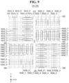
- FIG. 9 is a diagram illustrating an ROI for an overlay key area of FIG. 6 .
- the ROI setting (step S 130 refer to FIG. 3 ) of a method of manufacturing a semiconductor device according to some embodiments of the present disclosure will be described with reference to FIG. 9 .
- a description will be made focusing on differences from the ROI setting (step S 130 ) illustrated in FIG. 8 .
- At least a part of a first_first lower ROI R 310 _ 1 ′ may overlap a first_second lower ROI R 310 _ 2 ′, a first_fourth lower ROI R 310 _ 4 ′, and a first_fifth lower ROI R 310 _ 5 ′ in a plan view.
- At least a part of the first_second lower ROI R 310 _ 2 ′ may overlap the first_first lower ROI R 310 _ 1 ′, the first_third lower ROI R 310 _ 3 ′, the first_fourth lower ROI R 310 _ 4 ′, the first_fifth lower ROI R 310 _ 5 ′, and a first_sixth lower ROI R 310 _ 6 ′ in a plan view.
- At least a part of the first_third lower ROI R 310 _ 3 ′ may overlap the first_second lower ROI R 310 _ 2 ′, the first_fifth lower ROI R 310 _ 5 ′, and the first_sixth lower ROI R 310 _ 6 ′ in a plan view.
- At least a part of the first_fourth lower ROI R 310 _ 4 ′ may overlap the first_first lower ROI R 310 _ 1 ′, the first_second lower ROI R 310 _ 2 ′, and the first_fifth lower ROI R 310 _ 5 ′ in a plan view.
- At least a part of the first_fifth lower ROI R 310 _ 5 ′ may overlap the first_first lower ROI R 310 _ 1 ′, the first_second lower ROI R 310 _ 2 ′, the first_third lower ROI R 310 _ 3 ′, the first_fourth lower ROI R 310 _ 4 ′, and a first_sixth lower ROI R 310 _ 6 ′ in a plan view.
- At least a part of the first_sixth lower ROI R 310 _ 6 ′ may overlap the first_second lower ROI R 310 _ 2 ′, the first_third lower ROI R 310 _ 3 ′, and the first_fifth lower ROI R 310 _ 5 ′ in a plan view.
- the disposition relationship between the first to sixth lower ROIs R 310 _ 1 ′ to R 310 _ 6 ′ may also be applied to the disposition relationship between the second_first to second_sixth lower ROIs R 320 _ 1 ′ to R 320 _ 6 ′, the disposition relationship between the third_first to third_sixth lower ROIs R 330 _ 1 ′ to R 330 _ 6 ′, the disposition relationship between the fourth_first to fourth_sixth lower ROIs R 340 _ 1 ′ to R 340 _ 6 ′, the disposition relationship between the first_first to first_sixth upper ROIs R 410 _ 1 ′ to R 410 _ 6 ′, the disposition relationship between the second_first to second_sixth upper ROIs R 420 _ 1 ′ to R 420 _ 6 ′, the disposition relationship between the third_first to third_sixth upper ROIs R 430 _ 1 ′ to R 430 _ 6 ′, and the disposition relationship between the fourth_first
- a detection value of an overlay error is measured by measuring an overlay for a plurality of ROIs through the overlay error detection device 1 of FIG. 1 (step S 140 ).
- the overlay error detection device 1 of FIG. 1 may irradiate each ROI with the measurement light L (refer to FIG. 1 ) and measure the reflection light (i.e., reflected light of the measurement light L), thereby determining the degree of alignment of the pattern of the upper layer HL 1 ( FIG. 7 A ) with respect to the first lower layer LL 1 having the first to fourth lower overlay keys 310 to 340 , for example, and the components on the substrate 300 ( FIG. 7 A ).
- the overlay error detection device 1 may irradiate the first_first to fourth_first lower ROIs R 310 _ 1 to R 340 _ 1 and the first_first to fourth_first upper ROIs R 410 _ 1 to R 440 _ 1 simultaneously with a first measurement light L 1 that has a first center frequency ⁇ C_R_ 1 and a first bandwidth BW_R_ 1 , thereby performing each measurement of the first to fourth lower and upper ROIs R 310 to R 340 and R 410 to R 440 .
- the first_first to fourth_first lower ROIs R 310 _ 1 to R 340 _ 1 and the first_first to fourth_first upper ROIs R 410 _ 1 to R 440 _ 1 are collectively referred to as a first group R_ 1 .
- the degree of alignment in the second direction Y may be measured by irradiating the first_first and third_first lower ROIs R 310 _ 1 and R 330 _ 1 and the first_first and third_first upper ROIs R 410 _ 1 and R 430 _ 1 with the first measurement light L 1
- the degree of alignment in the first direction X may be measured by irradiating the second_first and fourth_first lower ROIs R 320 _ 1 and R 340 _ 1 and the second_first and fourth_first upper ROIs R 420 _ 1 and R 440 _ 1 with the first measurement light L 1 .
- the overlay error detection device 1 may measure a first kernel 3 sigma 3 ⁇ _R_ 1 , a first period ratio Periodic_Ratio_R_ 1 , and a first contrast CP_R_ 1 through the reflected first measurement light L 1 , and a first detection value Residual_R_ 1 of a first overlay error may be detected through the measurement values.
- the first detection value is a figure indicating the degree of the first overlay error.
- the first detection value may include or may be formed of percentage. The present invention is not limited thereto.
- the memory 220 of the overlay error detection device 1 may store the disposition information (e.g., locations within the semiconductor substrate 30 ) of the first_first to fourth_first lower ROIs R 310 _ 1 to R 340 _ 1 and the first_first to fourth_first upper ROIs R 410 _ 1 to R 440 _ 1 , the recipe information (e.g., the first center frequency ⁇ C_R_ 1 and the first bandwidth BW_R_ 1 ) for the first measurement light, a detection value for a first overlay error, and the like, in a first output file OutputFile_R_ 1 .
- the disposition information e.g., locations within the semiconductor substrate 30
- the recipe information e.g., the first center frequency ⁇ C_R_ 1 and the first bandwidth BW_R_ 1
- OutputFile_R_ 1 e.g., the first output file OutputFile_R_ 1 .
- the overlay error detection device 1 may irradiate the first_second to fourth_second lower ROIs R 310 _ 2 to R 340 _ 2 and the first_second to fourth_second upper ROIs R 410 _ 2 to R 440 _ 2 simultaneously with a second measurement light L 2 that has a second center frequency ⁇ C_R_ 2 and a second bandwidth BW_R_ 2 , thereby performing each measurement of the first to fourth lower and upper ROIs R 310 to R 340 and R 410 to R 440 .
- the first_second to fourth_second lower ROIs R 310 _ 2 to R 340 _ 2 and the first_second to fourth_second upper ROIs R 410 _ 2 to R 440 _ 2 are collectively referred to as a second group R_ 2 .
- the degree of alignment in the second direction Y may be measured by irradiating the first_second and third_second lower ROIs R 310 _ 2 and R 330 _ 2 and the first_second and third_second upper ROIs R 410 _ 2 and R 430 _ 2 with the second measurement light L 2
- the degree of alignment in the first direction X may be grasped by irradiating the second_second and fourth_second lower ROIs R 320 _ 2 and R 340 _ 2 and the second_second and fourth_second upper ROIs R 420 _ 2 and R 440 _ 2 with the second measurement light L 2 .
- the overlay error detection device 1 may measure a second kernel 3 sigma 3 ⁇ _R_ 2 , a second period ratio Periodic_Ratio_R_ 2 , and a second contrast CP_R_ 2 through the reflected second measurement light L 2 , and a second detection value Residual_R_ 2 of a second overlay error may be detected through the measurement values.
- the memory 220 of the overlay error detection device 1 may store the disposition information (e.g., locations within the semiconductor substrate 30 ) of the first_second to fourth_second lower ROIs R 310 _ 2 to R 340 _ 2 and the first_second to fourth_second upper ROIs R 410 _ 2 to R 440 _ 2 , the recipe information (e.g., the second center frequency ⁇ C_R_ 2 and the second bandwidth BW_R_ 2 ) for the second measurement light L 2 , a detection value for a second overlay error, and the like, in a second output file OutputFile_R_ 2 .
- the disposition information e.g., locations within the semiconductor substrate 30
- the recipe information e.g., the second center frequency ⁇ C_R_ 2 and the second bandwidth BW_R_ 2
- the overlay error detection device 1 may irradiate the first_third to fourth_third lower ROIs R 310 _ 3 to R 340 _ 3 and the first_third to fourth_third upper ROIs R 410 _ 3 to R 440 _ 3 simultaneously with a third measurement light that has a third center frequency ⁇ C_R_ 3 and a third bandwidth BW_R_ 3 , thereby performing each measurement of the first to fourth lower and upper ROIs R 310 to R 340 and R 410 to R 440 .
- the first_third to fourth_third lower ROIs R 310 _ 3 to R 340 _ 3 and the first_third to fourth_third upper ROIs R 410 _ 3 to R 440 _ 3 are collectively referred to as a third group R_ 3 .
- the degree of alignment in the second direction Y may be measured by irradiating the first_third and third-third lower ROIs R 310 _ 3 and R 330 _ 3 and the first_third and third-third upper ROIs R 410 _ 3 and R 430 _ 3 with the third measurement light
- the degree of alignment in the first direction X may be measured by irradiating the second-third and fourth_third lower ROIs R 320 _ 3 and R 340 _ 3 and the second-third and fourth_third upper ROIs R 420 _ 3 and R 440 _ 3 with the third measurement light.
- the overlay error detection device 1 may measure a third kernel 3 sigma 3 ⁇ _R_ 3 , a third period ratio Periodic_Ratio_R_ 3 , and a third contrast CP_R_ 3 through the reflected third measurement light, and a third detection value Residual_R_ 3 of a third overlay error may be detected through the measurement value.
- the memory 220 of the overlay error detection device 1 may store the disposition information of the first_third to fourth_third lower ROIs R 310 _ 3 to R 340 _ 3 and the first_third to fourth_third upper ROIs R 410 _ 3 to R 440 _ 3 , the recipe information for the third measurement light, a detection value for a first overlay error, and the like, in a third output file OutputFile_R_ 3 .
- the overlay error detection device 1 may irradiate the first_fourth to fourth_fourth lower ROIs R 310 _ 4 to R 340 _ 4 and the first_fourth to fourth_fourth upper ROIs R 410 _ 4 to R 440 _ 4 simultaneously with a fourth measurement light that has a fourth center frequency ⁇ C_R_ 4 and a fourth bandwidth BW_R_ 4 , thereby performing each measurement of the first to fourth lower and upper ROIs R 310 to R 340 and R 410 to R 440 .
- the first_fourth to fourth_fourth lower ROIs R 310 _ 4 to R 340 _ 4 and the first_fourth to fourth_fourth upper ROIs R 410 _ 4 to R 440 _ 4 are collectively referred to as a fourth group R_ 4 .
- the degree of alignment in the second direction Y may be measured by irradiating the first_fourth and third_fourth lower ROIs R 310 _ 4 and R 330 _ 4 and the first_fourth and third_fourth upper ROIs R 410 _ 4 and R 430 _ 4 with the fourth measurement light
- the degree of alignment in the first direction X may be measured by irradiating the second_fourth and fourth_fourth lower ROIs R 320 _ 4 and R 340 _ 4 and the second_fourth and fourth_fourth upper ROIs R 420 _ 4 and R 440 _ 4 with the fourth measurement light.
- the overlay error detection device 1 may measure a fourth kernel 3 sigma 3 ⁇ _R_ 4 , a fourth period ratio Periodic_Ratio_R_ 4 , and a fourth contrast CP_R_ 4 through the reflected fourth measurement light, and a fourth detection value Residual_R_ 1 of a fourth overlay error may be detected through the measurement values.
- the memory 220 of the overlay error detection device 1 may store the disposition information (e.g., locations within the semiconductor substrate 30 ) of the first_fourth to fourth_fourth lower ROIs R 310 _ 4 to R 340 _ 4 and the first_fourth to fourth_fourth upper ROIs R 410 _ 4 to R 440 _ 4 , the recipe information (e.g., the fourth center frequency ⁇ C_R_ 4 and the fourth bandwidth BW_R_ 4 ) for the fourth measurement light, a detection value for a fourth overlay error, and the like, in a fourth output file OutputFile_R_ 1 .
- the disposition information e.g., locations within the semiconductor substrate 30
- the recipe information e.g., the fourth center frequency ⁇ C_R_ 4 and the fourth bandwidth BW_R_ 4
- the overlay error detection device 1 may irradiate the first_fifth to fourth_fifth lower ROIs R 310 _ 5 to R 340 _ 5 and the first_fifth to fourth_fifth upper ROIs R 410 _ 5 to R 440 _ 5 simultaneously with a fifth measurement light that has a fifth center frequency ⁇ C_R_ 5 and a fifth bandwidth BW_R_ 5 , thereby performing each measurement of the first to fourth lower and upper ROIs R 310 to R 340 and R 410 to R 440 .
- the first_fifth to fourth_fifth lower ROIs R 310 _ 5 to R 340 _ 5 and the first_fifth to fourth_fifth upper ROIs R 410 _ 5 to R 440 _ 5 are collectively referred to as a fifth group R_ 5 .
- the degree of alignment in the second direction Y may be measured by irradiating the first_fifth and third_fifth lower ROIs R 310 _ 5 and R 330 _ 5 and the first_fifth and third_fifth upper ROIs R 410 _ 5 and R 430 _ 5 with the fifth measurement light
- the degree of alignment in the first direction X may be measured by irradiating the second_fifth and fourth_fifth lower ROIs R 320 _ 5 and R 340 _ 5 and the second_fifth and fourth_fifth upper ROIs R 420 _ 5 and R 440 _ 5 with the fifth measurement light.
- the overlay error detection device 1 may measure a fifth kernel 3 sigma 3 ⁇ _R_ 5 , a fifth period ratio Periodic_Ratio_R_ 5 , and a fifth contrast CP_R_ 5 through the reflected fifth measurement light, and a fifth detection value Residual_R_ 5 of a fifth overlay error may be detected through the measurement values.
- the memory 220 of the overlay error detection device 1 may store the disposition information (e.g., locations within the semiconductor substrate 30 ) of the first_fifth to fourth_fifth lower ROIs R 310 _ 5 to R 340 _ 5 and the first_fifth to fourth_fifth upper ROIs R 410 _ 5 to R 440 _ 5 , the recipe information (e.g., the fifth center frequency ⁇ C_R_ 5 and the fifth bandwidth BW_R_ 5 ) for the fifth measurement light, a detection value for a fifth overlay error, and the like, in a fifth output file OutputFile_R_ 5 .
- the disposition information e.g., locations within the semiconductor substrate 30
- the recipe information e.g., the fifth center frequency ⁇ C_R_ 5 and the fifth bandwidth BW_R_ 5
- OutputFile_R_ 5 e.g., the fourth output file
- the overlay error detection device 1 may irradiate the first_sixth to fourth_sixth lower ROIs R 310 _ 6 to R 340 _ 6 and the first_sixth to fourth_sixth upper ROIs R 410 _ 6 to R 440 _ 6 simultaneously with a sixth measurement light that has a sixth center frequency ⁇ C_R_ 6 and a sixth bandwidth BW_R_ 6 , thereby performing each measurement of the first to fourth lower and upper ROIs R 310 to R 340 and R 410 to R 440 .
- the first_sixth to fourth_sixth lower ROIs R 310 _ 6 to R 340 _ 6 and the first_sixth to fourth_sixth upper ROIs R 410 _ 6 to R 440 _ 6 are collectively referred to as a sixth group R_ 6 .
- the degree of alignment in the second direction Y may be measured by irradiating the first_sixth and third_sixth lower ROIs R 310 _ 6 and R 330 _ 6 and the first_sixth and third_sixth upper ROIs R 410 _ 6 and R 430 _ 6 with the sixth measurement light
- the degree of alignment in the first direction X may be measured by irradiating the second_sixth and fourth_sixth lower ROIs R 320 _ 6 and R 340 _ 6 and the second_sixth and fourth_sixth upper ROIs R 420 _ 6 and R 440 _ 6 with the sixth measurement light.
- the overlay error detection device 1 may measure a sixth kernel 3 sigma 3 ⁇ _R_ 6 , a sixth period ratio Periodic_Ratio_R_ 6 , and a sixth contrast CP_R_ 6 through the reflected sixth measurement light, and a sixth detection value Residual_R_ 6 of a sixth overlay error may be detected through the measurement values.
- the memory 220 of the overlay error detection device 1 may store the disposition information (e.g., locations within the semiconductor substrate 30 ) of the first_sixth to fourth_sixth lower ROIs R 310 _ 6 to R 340 _ 6 and the first_sixth to fourth_sixth upper ROIs R 410 _ 6 to R 440 _ 6 , the recipe information (e.g., the sixth center frequency ⁇ C_R_ 6 and the sixth bandwidth BW_R_ 6 ) for the sixth measurement light, a detection value for a sixth overlay error, and the like, in a sixth output file OutputFile_R_ 6 .
- the disposition information e.g., locations within the semiconductor substrate 30
- the recipe information e.g., the sixth center frequency ⁇ C_R_ 6 and the sixth bandwidth BW_R_ 6
- a kernel 3 sigma value for a third group R_ 3 corresponding to the first_third to fourth_third lower ROIs R 310 _ 3 to R 340 _ 3 and the first_third to fourth_third upper ROIs R 410 _ 3 to R 440 _ 3 is measured to be the lowest among the first to sixth groups R_ 1 to R_ 6 . This is because in the first_third to fourth_third lower ROIs R 310 _ 3 to R 340 _ 3 , the measurement is not performed on the first_first lower pattern 311 and the second_fourth to second_sixth lower patterns 324 to 326 , which are defective patterns in which a partial area has been damaged.
- the overlay error detection device 1 may set an ROI by avoiding the first, fifth, and sixth groups R_ 1 , R_ 5 , and R_ 6 that exceed a predetermined threshold value a of the Kernel 3 sigma.
- the predetermined threshold value a may be empirically determined.
- it may also check the fluctuation of the detection value in which the kernel 3 sigma value fluctuates even at the same ROI according to the fluctuation of the center wavelength ⁇ of the measurement light L.
- the overlay error detection device 1 sets an adjusted ROI for an overlay key based on the detection value of the overlay error of FIGS. 11 and 12 (step S 150 ).
- the overlay error detection device 1 sets the first lower ROI R 310 over the first_second to first_sixth lower patterns 311 to 315 with respect to the first lower overlay key 310 , and has a long side with a length of a third width Wa′ and a short side with a length of a fourth width Wb′.
- the first ROI R 310 does not overlap the first_first lower pattern 311 which is damaged.
- the second lower ROI R 320 is set over the second_second to second_sixth lower patterns 322 to 326 , and has a long side with a length of a third width Wa′ and a short side with a length of a fourth width Wb′.
- the second lower ROI R 320 may overlap portions of the second_second to second_sixth lower patterns 322 to 326 , without overlapping damage portions of thereof.
- the third lower ROI R 330 is set over the third_second to third_sixth lower patterns 332 to 336 , and has a long side with a length of a third width Wa′ and a short side with a length of a fourth width Wb′.
- the fourth lower ROI R 340 is set over the fourth_second to fourth_sixth lower patterns 342 to 346 , and has a long side with a length of a third width Wa′ and a short side with a length of a fourth width Wb′.
- the length of the third width Wa′ may be different from the first width Wa of FIG. 8
- the length of the fourth width Wb′ may be different from the second width Wb of FIG. 8
- the length of the third width Wa′ may be greater than the first width Wa
- the length of the fourth width Wb′ may be greater than the second width Wb.
- a detection value of an overlay error is measured by measuring an overlay for an adjusted ROI through the overlay error detection device 1 (step S 160 ).
- the overlay error detection device 1 may irradiate each adjusted ROI with the measurement light L (refer to FIG. 1 ) and measure the reflection light, thereby determining the degree of alignment of the pattern of the upper layer HL 1 ( FIG. 7 A ) and the components on the substrate 300 ( FIG. 7 A ).
- the overlay error detection device 1 performs the steps S 130 and S 140 to set an adjusted ROI, measure the overlay, and measure the detection value of the overlay error.
- the adjusted ROI not only the overlay measurement may be performed excluding the defective pattern, but also the recipe of the measurement light may be optimized according to the recipe information of the measurement light, and thus, the reliability of the overlay measurement may be improved.
- FIG. 14 is a diagram illustrating an overlay key of a semiconductor substrate according to some embodiments of the present disclosure.
- an overlay key area OA 2 of the semiconductor substrate 30 will be described with reference to FIG. 14 .
- a description will be made focusing on differences from the overlay key area OA 1 illustrated in FIG. 6 .
- Fifth and sixth lower overlay keys 350 and 360 and fifth and sixth upper overlay keys 450 and 460 may be disposed on the overlay key area OA 2 .
- the fifth lower overlay key 350 may include fifth_first to fifth_sixth lower patterns 351 to 356
- the sixth lower overlay key 360 may include sixth_first to sixth_sixth lower patterns 361 to 366
- the fifth upper overlay key 450 may include fifth_first to fifth_sixth upper patterns 451 to 456
- the sixth upper overlay key 460 may include sixth_first to sixth_sixth upper patterns 461 to 466 .
- the fifth and sixth lower overlay keys 350 and 360 may correspond to the first and second lower overlay keys 310 and 320 of FIG. 6 , respectively, and the fifth and sixth upper overlay keys 450 and 460 may correspond to the first and second upper overlay keys 410 and 420 of FIG. 6 , respectively.
- the fifth lower overlay key 350 may overlap the fifth upper overlay key 450 in a plan view
- the sixth lower overlay key 360 may overlap the sixth upper overlay key 460 in a plan view
- the fifth_first to fifth_sixth lower patterns 351 to 356 included in the fifth lower overlay key 350 do not overlap the fifth_first to fifth_sixth upper patterns 451 to 456 included in the fifth upper overlay key 450 in a plan view.
- the fifth_first to fifth_sixth lower patterns 351 to 356 , and the fifth_first to fifth_sixth upper patterns 451 to 456 may be alternately arranged in the second direction Y.
- the fifth_second lower pattern 452 may be disposed between the fifth_first and fifth_second upper patterns 451 and 452
- the fifth_first upper pattern 451 may be disposed between the fifth_first and fifth_second lower patterns 351 and 352 .
- This disposition may also be applied to the sixth lower overlay key 360 and the sixth upper overlay key 460 .
Landscapes
- Physics & Mathematics (AREA)
- General Physics & Mathematics (AREA)
- Engineering & Computer Science (AREA)
- Manufacturing & Machinery (AREA)
- Computer Hardware Design (AREA)
- Microelectronics & Electronic Packaging (AREA)
- Power Engineering (AREA)
- Condensed Matter Physics & Semiconductors (AREA)
- Exposure And Positioning Against Photoresist Photosensitive Materials (AREA)
Abstract
Description
Claims (20)
Applications Claiming Priority (2)
| Application Number | Priority Date | Filing Date | Title |
|---|---|---|---|
| KR1020200166728A KR20220077615A (en) | 2020-12-02 | 2020-12-02 | A method of manufacturing a semiconductor device |
| KR10-2020-0166728 | 2020-12-02 |
Publications (2)
| Publication Number | Publication Date |
|---|---|
| US20220172944A1 US20220172944A1 (en) | 2022-06-02 |
| US12068157B2 true US12068157B2 (en) | 2024-08-20 |
Family
ID=81752843
Family Applications (1)
| Application Number | Title | Priority Date | Filing Date |
|---|---|---|---|
| US17/385,069 Active 2042-10-15 US12068157B2 (en) | 2020-12-02 | 2021-07-26 | Method of manufacturing semiconductor device |
Country Status (2)
| Country | Link |
|---|---|
| US (1) | US12068157B2 (en) |
| KR (1) | KR20220077615A (en) |
Citations (11)
| Publication number | Priority date | Publication date | Assignee | Title |
|---|---|---|---|---|
| US6486954B1 (en) | 2000-09-01 | 2002-11-26 | Kla-Tencor Technologies Corporation | Overlay alignment measurement mark |
| US6819426B2 (en) * | 2001-02-12 | 2004-11-16 | Therma-Wave, Inc. | Overlay alignment metrology using diffraction gratings |
| JP2005317617A (en) | 2004-04-27 | 2005-11-10 | Nikon Corp | Position detection mark and reticle or photosensitive substrate including the same, position detection method, mark evaluation method, mark detection method and mark detection apparatus, and exposure method and exposure apparatus |
| KR101476080B1 (en) | 2010-08-03 | 2014-12-23 | 케이엘에이-텐코 코포레이션 | Multi-layer overlay metrology target and complimentary overlay metrology measurement systems |
| USRE45943E1 (en) * | 2007-03-14 | 2016-03-22 | Taiwan Semiconductor Manufacturing Company, Ltd. | Measurement of overlay offset in semiconductor processing |
| US9811003B2 (en) | 2012-05-29 | 2017-11-07 | Asml Netherlands B.V. | Metrology method and apparatus, substrate, lithographic system and device manufacturing method |
| US10289008B2 (en) | 2016-12-09 | 2019-05-14 | Asml Netherlands B.V. | Methods and apparatus for predicting performance of a measurement method, measurement method and apparatus |
| US20190250521A1 (en) | 2013-05-30 | 2019-08-15 | Kla-Tencor Corporation | Combined imaging and scatterometry metrology |
| CN111123662A (en) | 2020-01-19 | 2020-05-08 | 中国科学院微电子研究所 | Method and device for acquiring overlay error measurement data |
| US10990023B1 (en) * | 2020-02-27 | 2021-04-27 | Taiwan Semiconductor Manufacturing Co., Ltd. | Method and apparatus for diffraction-based overlay measurement |
| US20210199596A1 (en) * | 2019-12-27 | 2021-07-01 | Canon Kabushiki Kaisha | Inspection apparatus and manufacturing method for semiconductor device |
-
2020
- 2020-12-02 KR KR1020200166728A patent/KR20220077615A/en not_active Ceased
-
2021
- 2021-07-26 US US17/385,069 patent/US12068157B2/en active Active
Patent Citations (11)
| Publication number | Priority date | Publication date | Assignee | Title |
|---|---|---|---|---|
| US6486954B1 (en) | 2000-09-01 | 2002-11-26 | Kla-Tencor Technologies Corporation | Overlay alignment measurement mark |
| US6819426B2 (en) * | 2001-02-12 | 2004-11-16 | Therma-Wave, Inc. | Overlay alignment metrology using diffraction gratings |
| JP2005317617A (en) | 2004-04-27 | 2005-11-10 | Nikon Corp | Position detection mark and reticle or photosensitive substrate including the same, position detection method, mark evaluation method, mark detection method and mark detection apparatus, and exposure method and exposure apparatus |
| USRE45943E1 (en) * | 2007-03-14 | 2016-03-22 | Taiwan Semiconductor Manufacturing Company, Ltd. | Measurement of overlay offset in semiconductor processing |
| KR101476080B1 (en) | 2010-08-03 | 2014-12-23 | 케이엘에이-텐코 코포레이션 | Multi-layer overlay metrology target and complimentary overlay metrology measurement systems |
| US9811003B2 (en) | 2012-05-29 | 2017-11-07 | Asml Netherlands B.V. | Metrology method and apparatus, substrate, lithographic system and device manufacturing method |
| US20190250521A1 (en) | 2013-05-30 | 2019-08-15 | Kla-Tencor Corporation | Combined imaging and scatterometry metrology |
| US10289008B2 (en) | 2016-12-09 | 2019-05-14 | Asml Netherlands B.V. | Methods and apparatus for predicting performance of a measurement method, measurement method and apparatus |
| US20210199596A1 (en) * | 2019-12-27 | 2021-07-01 | Canon Kabushiki Kaisha | Inspection apparatus and manufacturing method for semiconductor device |
| CN111123662A (en) | 2020-01-19 | 2020-05-08 | 中国科学院微电子研究所 | Method and device for acquiring overlay error measurement data |
| US10990023B1 (en) * | 2020-02-27 | 2021-04-27 | Taiwan Semiconductor Manufacturing Co., Ltd. | Method and apparatus for diffraction-based overlay measurement |
Also Published As
| Publication number | Publication date |
|---|---|
| US20220172944A1 (en) | 2022-06-02 |
| KR20220077615A (en) | 2022-06-09 |
Similar Documents
| Publication | Publication Date | Title |
|---|---|---|
| CN104781650B (en) | For high aspect ratio and the gauging system and method for big lateral dimension structure | |
| JP4196319B2 (en) | Overlay measurement method | |
| CN110062952B (en) | Simultaneous multi-angle spectroscopy | |
| JP4864290B2 (en) | Method and structure for calibrating measurement tools based on non-destructive lightwave measurements (scatterometry) used to measure the dimensions of structures on semiconductor devices | |
| US6479200B1 (en) | Method of controlling stepper process parameters based upon scatterometric measurements of DICD features | |
| US7642550B2 (en) | Multi-layer structures for parameter measurement | |
| US6643008B1 (en) | Method of detecting degradation in photolithography processes based upon scatterometric measurements of grating structures, and a device comprising such structures | |
| US12142537B2 (en) | Defect measurement method | |
| US6529282B1 (en) | Method of controlling photolithography processes based upon scatterometric measurements of photoresist thickness, and system for accomplishing same | |
| WO2022183639A1 (en) | Semiconductor structure measuring method, and device | |
| US12068157B2 (en) | Method of manufacturing semiconductor device | |
| US12451352B2 (en) | Method for fabricating semiconductor device | |
| CN100416821C (en) | Semiconductor device with measurement pattern and measurement method thereof | |
| US6582863B1 (en) | Method of controlling photolithography processes based upon scatterometric measurements of sub-nominal grating structures | |
| Sendelbach et al. | Use of multiple azimuthal angles to enable advanced scatterometry applications | |
| US20250076185A1 (en) | Angle Of Incidence And Azimuth Angle Resolved Spectroscopic Ellipsometry For Semiconductor Metrology | |
| JP7463551B2 (en) | Trench optical measurement target | |
| US20250147409A1 (en) | Method for manufacturing semiconductor device | |
| Medikonda et al. | Scatterometry-based methodologies for characterization of MRAM technology | |
| KR100672691B1 (en) | Pattern measuring method of semiconductor device | |
| US12131111B2 (en) | Method, apparatus and device for measuring semiconductor structure | |
| US20230109008A1 (en) | Spectroscopic Reflectometry And Ellipsometry Measurements With Electroreflectance Modulation | |
| US20250164872A1 (en) | Semiconductor structure inspection method, extreme ultraviolet (euv) mask inspection method, and euv lithography method | |
| US20250105064A1 (en) | Electrical Performance Prediction Based On Structural Measurements Of Partially Fabricated Semiconductor Devices | |
| CN121096888A (en) | Testing methods, apparatus, equipment, media and procedures products |
Legal Events
| Date | Code | Title | Description |
|---|---|---|---|
| FEPP | Fee payment procedure |
Free format text: ENTITY STATUS SET TO UNDISCOUNTED (ORIGINAL EVENT CODE: BIG.); ENTITY STATUS OF PATENT OWNER: LARGE ENTITY |
|
| AS | Assignment |
Owner name: SAMSUNG ELECTRONICS CO., LTD., KOREA, REPUBLIC OF Free format text: ASSIGNMENT OF ASSIGNORS INTEREST;ASSIGNORS:HA, HYUN SEUNG;KIM, JANG HOON;KIM, TAE-KYU;AND OTHERS;REEL/FRAME:057133/0392 Effective date: 20210716 |
|
| STPP | Information on status: patent application and granting procedure in general |
Free format text: DOCKETED NEW CASE - READY FOR EXAMINATION |
|
| STPP | Information on status: patent application and granting procedure in general |
Free format text: NON FINAL ACTION MAILED |
|
| STPP | Information on status: patent application and granting procedure in general |
Free format text: RESPONSE TO NON-FINAL OFFICE ACTION ENTERED AND FORWARDED TO EXAMINER |
|
| STPP | Information on status: patent application and granting procedure in general |
Free format text: NOTICE OF ALLOWANCE MAILED -- APPLICATION RECEIVED IN OFFICE OF PUBLICATIONS |
|
| ZAAB | Notice of allowance mailed |
Free format text: ORIGINAL CODE: MN/=. |
|
| STPP | Information on status: patent application and granting procedure in general |
Free format text: PUBLICATIONS -- ISSUE FEE PAYMENT VERIFIED |
|
| STCF | Information on status: patent grant |
Free format text: PATENTED CASE |