US12068028B2 - Circuitry for parallel set and reset of resistive random-access memory (ReRAM) cells - Google Patents
Circuitry for parallel set and reset of resistive random-access memory (ReRAM) cells Download PDFInfo
- Publication number
- US12068028B2 US12068028B2 US17/653,353 US202217653353A US12068028B2 US 12068028 B2 US12068028 B2 US 12068028B2 US 202217653353 A US202217653353 A US 202217653353A US 12068028 B2 US12068028 B2 US 12068028B2
- Authority
- US
- United States
- Prior art keywords
- reram
- input
- output
- programming
- port
- Prior art date
- Legal status (The legal status is an assumption and is not a legal conclusion. Google has not performed a legal analysis and makes no representation as to the accuracy of the status listed.)
- Active, expires
Links
- 230000015654 memory Effects 0.000 title claims abstract description 13
- 230000005669 field effect Effects 0.000 claims description 4
- 239000012212 insulator Substances 0.000 claims description 2
- 229910052710 silicon Inorganic materials 0.000 claims description 2
- 239000010703 silicon Substances 0.000 claims description 2
- 238000000034 method Methods 0.000 abstract description 16
- 238000010586 diagram Methods 0.000 description 10
- 238000012795 verification Methods 0.000 description 4
- 230000008901 benefit Effects 0.000 description 3
- 230000007423 decrease Effects 0.000 description 2
- 230000007812 deficiency Effects 0.000 description 2
- 230000006870 function Effects 0.000 description 2
- XOJVVFBFDXDTEG-UHFFFAOYSA-N Norphytane Natural products CC(C)CCCC(C)CCCC(C)CCCC(C)C XOJVVFBFDXDTEG-UHFFFAOYSA-N 0.000 description 1
- 238000003491 array Methods 0.000 description 1
- 230000000694 effects Effects 0.000 description 1
- 238000010200 validation analysis Methods 0.000 description 1
Images


Classifications
-
- G—PHYSICS
- G11—INFORMATION STORAGE
- G11C—STATIC STORES
- G11C16/00—Erasable programmable read-only memories
- G11C16/02—Erasable programmable read-only memories electrically programmable
- G11C16/06—Auxiliary circuits, e.g. for writing into memory
- G11C16/10—Programming or data input circuits
-
- G—PHYSICS
- G11—INFORMATION STORAGE
- G11C—STATIC STORES
- G11C13/00—Digital stores characterised by the use of storage elements not covered by groups G11C11/00, G11C23/00, or G11C25/00
- G11C13/0002—Digital stores characterised by the use of storage elements not covered by groups G11C11/00, G11C23/00, or G11C25/00 using resistive RAM [RRAM] elements
- G11C13/0021—Auxiliary circuits
- G11C13/0023—Address circuits or decoders
- G11C13/0026—Bit-line or column circuits
-
- G—PHYSICS
- G11—INFORMATION STORAGE
- G11C—STATIC STORES
- G11C13/00—Digital stores characterised by the use of storage elements not covered by groups G11C11/00, G11C23/00, or G11C25/00
- G11C13/0002—Digital stores characterised by the use of storage elements not covered by groups G11C11/00, G11C23/00, or G11C25/00 using resistive RAM [RRAM] elements
- G11C13/0021—Auxiliary circuits
- G11C13/0023—Address circuits or decoders
- G11C13/0028—Word-line or row circuits
-
- G—PHYSICS
- G11—INFORMATION STORAGE
- G11C—STATIC STORES
- G11C13/00—Digital stores characterised by the use of storage elements not covered by groups G11C11/00, G11C23/00, or G11C25/00
- G11C13/0002—Digital stores characterised by the use of storage elements not covered by groups G11C11/00, G11C23/00, or G11C25/00 using resistive RAM [RRAM] elements
- G11C13/0021—Auxiliary circuits
- G11C13/0038—Power supply circuits
-
- G—PHYSICS
- G11—INFORMATION STORAGE
- G11C—STATIC STORES
- G11C13/00—Digital stores characterised by the use of storage elements not covered by groups G11C11/00, G11C23/00, or G11C25/00
- G11C13/0002—Digital stores characterised by the use of storage elements not covered by groups G11C11/00, G11C23/00, or G11C25/00 using resistive RAM [RRAM] elements
- G11C13/0021—Auxiliary circuits
- G11C13/004—Reading or sensing circuits or methods
-
- G—PHYSICS
- G11—INFORMATION STORAGE
- G11C—STATIC STORES
- G11C13/00—Digital stores characterised by the use of storage elements not covered by groups G11C11/00, G11C23/00, or G11C25/00
- G11C13/0002—Digital stores characterised by the use of storage elements not covered by groups G11C11/00, G11C23/00, or G11C25/00 using resistive RAM [RRAM] elements
- G11C13/0021—Auxiliary circuits
- G11C13/0064—Verifying circuits or methods
-
- G—PHYSICS
- G11—INFORMATION STORAGE
- G11C—STATIC STORES
- G11C13/00—Digital stores characterised by the use of storage elements not covered by groups G11C11/00, G11C23/00, or G11C25/00
- G11C13/0002—Digital stores characterised by the use of storage elements not covered by groups G11C11/00, G11C23/00, or G11C25/00 using resistive RAM [RRAM] elements
- G11C13/0021—Auxiliary circuits
- G11C13/0069—Writing or programming circuits or methods
-
- G—PHYSICS
- G11—INFORMATION STORAGE
- G11C—STATIC STORES
- G11C13/00—Digital stores characterised by the use of storage elements not covered by groups G11C11/00, G11C23/00, or G11C25/00
- G11C13/0002—Digital stores characterised by the use of storage elements not covered by groups G11C11/00, G11C23/00, or G11C25/00 using resistive RAM [RRAM] elements
- G11C13/0021—Auxiliary circuits
- G11C13/0097—Erasing, e.g. resetting, circuits or methods
-
- G—PHYSICS
- G11—INFORMATION STORAGE
- G11C—STATIC STORES
- G11C16/00—Erasable programmable read-only memories
- G11C16/02—Erasable programmable read-only memories electrically programmable
- G11C16/06—Auxiliary circuits, e.g. for writing into memory
- G11C16/34—Determination of programming status, e.g. threshold voltage, overprogramming or underprogramming, retention
- G11C16/3404—Convergence or correction of memory cell threshold voltages; Repair or recovery of overerased or overprogrammed cells
-
- G—PHYSICS
- G11—INFORMATION STORAGE
- G11C—STATIC STORES
- G11C13/00—Digital stores characterised by the use of storage elements not covered by groups G11C11/00, G11C23/00, or G11C25/00
- G11C13/0002—Digital stores characterised by the use of storage elements not covered by groups G11C11/00, G11C23/00, or G11C25/00 using resistive RAM [RRAM] elements
- G11C13/0021—Auxiliary circuits
- G11C13/003—Cell access
-
- G—PHYSICS
- G11—INFORMATION STORAGE
- G11C—STATIC STORES
- G11C13/00—Digital stores characterised by the use of storage elements not covered by groups G11C11/00, G11C23/00, or G11C25/00
- G11C13/0002—Digital stores characterised by the use of storage elements not covered by groups G11C11/00, G11C23/00, or G11C25/00 using resistive RAM [RRAM] elements
- G11C13/0021—Auxiliary circuits
- G11C13/0069—Writing or programming circuits or methods
- G11C2013/0076—Write operation performed depending on read result
-
- G—PHYSICS
- G11—INFORMATION STORAGE
- G11C—STATIC STORES
- G11C13/00—Digital stores characterised by the use of storage elements not covered by groups G11C11/00, G11C23/00, or G11C25/00
- G11C13/0002—Digital stores characterised by the use of storage elements not covered by groups G11C11/00, G11C23/00, or G11C25/00 using resistive RAM [RRAM] elements
- G11C13/0021—Auxiliary circuits
- G11C13/0069—Writing or programming circuits or methods
- G11C2013/0078—Write using current through the cell
-
- G—PHYSICS
- G11—INFORMATION STORAGE
- G11C—STATIC STORES
- G11C2213/00—Indexing scheme relating to G11C13/00 for features not covered by this group
- G11C2213/70—Resistive array aspects
- G11C2213/79—Array wherein the access device being a transistor
-
- G—PHYSICS
- G11—INFORMATION STORAGE
- G11C—STATIC STORES
- G11C2213/00—Indexing scheme relating to G11C13/00 for features not covered by this group
- G11C2213/70—Resistive array aspects
- G11C2213/82—Array having, for accessing a cell, a word line, a bit line and a plate or source line receiving different potentials
Definitions
- the invention generally relates to resistive random-access memory (ReRAM) arrays, and more particularly to the programming of a plurality of ReRAM cells.
- ReRAM resistive random-access memory
- Resistive random-access memories are, unlike, for example, Flash memory cells, bit programmable. That is, every bit of the array may be programmed separately from any other bit being programmed. When used in random access mode, write-over is permitted, meaning that a bit may be flipped from ‘0’ to ‘1’ (set) or from ‘1’ to ‘0’ (reset). For example, a set operation may be deemed to decrease the resistance of the resistive element of the ReRAM cell, while a reset operation may be deemed to increase the resistance of the resistive element of the ReRAM cell. In order to perform the programming of a ReRAM cell, the process described in FIG. 1 is used. For example, a byte of memory contains ‘00110101’.
- the new data is compared to the old data so as to establish which bits need to be changed. This has to be separated between bits that require to be ‘set’ (for example, changed from ‘0’ to ‘1’) and bits to be ‘reset’ (for example, need to be changed from ‘1’ to ‘0’). That requires the creation of masks to allow proper programming of the respective cells. Thereafter, for example, the ‘set’ process takes place, then a verification, thereafter the ‘reset’ process takes place, and this is verified too. The ‘reset’ is performed after the ‘set’ operation.
- the overall time to program the ReRAM word includes the serial time it takes to set and reset the bits plus other overhead activities, such as the creation of masks and the validation.
- the ReRAM array comprises: a plurality of ReRAM cells arranged in an array, wherein the array includes a plurality of rows and a plurality of columns, wherein at least two ReRAM cells of an array includes a word, wherein each ReRAM cell includes a select device having a control port, a first port, and a second port, such that under the control of a signal applied to the control port, current may flow or not flow between the first port and the second port, and a resistive element including a top electrode (TE) and a bottom electrode (BE), wherein the control port is connected to a word line, the first port connected to a source line, the TE connected to a bit line, and the second port is connected to the BE; and a plurality of controllers, wherein the output of each of the plurality of controllers cause a reset programming or a set programming of the ReRAM cell in the column of the plurality of ReRAM cells that has
- Certain embodiments disclosed herein include a method for parallel reset and set programming of a resistive random-access memory (ReRAM) word of a ReRAM array.
- the method comprises: receiving a new word to be programmed into the ReRAM word of the ReRAM array, wherein the new word contains a plurality of bits, each bit corresponding to a ReRAM cell; comparing a content of the ReRAM word to be programmed to the received new word; determining, based on the comparison, a plurality of enable signals to each source line and bit line of the ReRAM word to be programmed; generating a mask to disable programming of a first portion of the plurality of bits of the ReRAM word that are not to be programmed and enable programming of a second portion of the plurality of bits of the ReRAM word that are to be programmed; performing parallel reset and set programming of the ReRAM word to be programmed while applying the mask; terminating programming upon checking the content of the ReRAM word that was programmed to be successful; and repeating programming upon determination that the content of the ReRAM word does not match
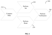
- FIG. 2 is a flow diagram of a process to perform programming of a plurality of ReRAM cells according to an embodiment.
- FIG. 3 is a schematic diagram of a ReRAM array equipped with bit line and bit source controllers for parallel reset and set programming according to an embodiment.
- FIG. 4 is a schematic diagram of a programming termination circuitry according to an embodiment.
- FIG. 5 is a flowchart of a parallel reset and set programming of a ReRAM word according to an embodiment.
- FIG. 6 is a schematic timing diagram for parallel programming of ReRAM cells of the same word according to an embodiment.
- the term “programming” may refer herein to the initial setting of the resistor from its pristine condition, also known as forming of the ReRAM resistor. It may further refer to either set or reset of the ReRAM resistor as the case may be. The discussion below is with regard to either the form-programming or set-programming of the ReRAM resistive element. However, it should be noted that the circuits may be so adapted to handle also reset-programming without departing from the scope of the present disclosure.
- a circuitry for increasing programming speed of a resistive random-access memory (ReRAM) word by performing parallel set and reset operation is presented. It thereby overcomes deficiencies of serial set and reset programming of ReRAM cells and speeds up the programming process.
- Control circuitry is provided for smart parallel programming of a word line of the ReRAM array. Cells that do not have to be changed in a word line are masked. A method of operation of the circuitry achieves such parallel programming process.
- FIG. 2 depicts a flow diagram 200 of a process to perform programming of a plurality of ReRAM cells according to an embodiment.
- comparison of data takes place. That is, if, for example, a byte of memory contains ‘00110101’ to be changed to ‘01011100.’ the first, fourth, sixth, and seventh bits, beginning from the left, do not need to be changed. The bits to retain unchanged may be masked from being changed as further described herein. For example, such a mask in this case may be 01101001, where a ‘1’ designates a bit that needs to be programmed, i.e., set or reset as the case may be.
- the second and fifth bits of the ReRAM word need to be ‘set’, i.e., be flipped from ‘0’ to ‘1’, while the third and eighth bits of the ReRAM word need to be ‘reset’, i.e., be flipped from ‘1’ to ‘0’.
- a ‘set’ programming may be performed to flip a bit of the ReRAM word from, for example, ‘0’ to ‘1’.
- a ‘reset’ programming may be performed to flip a bit of the ReRAM word from, for example, ‘1’ to ‘0’.
- Reset and set are opposite operations. It should be appreciated that, in an embodiment, the logical function of set programming and reset may be the opposite of the description provided herein, i.e., set may mean flipping from ‘1’ to ‘0’ and reset flipping a bit from ‘0’ to ‘1’ that is only the logical association of the operations performed.
- the provided circuitry and method of operation allow parallel performance of the ‘reset’ 230 and ‘set’ 220 operations. Thereafter, at 240 , verification may be performed to verify that the desired new data was written into the ReRAM word.
- the programming steps presented herein that allow parallel programming may provide a significant speed advantage over the solutions discussed in the related art that performs step-by-step sequential programming and verification.
- FIG. 3 is an example schematic diagram 300 of a ReRAM array equipped with bit line 340 , source line 330 , and controllers 350 for parallel reset and set programming according to an embodiment.
- a portion of a ReRAM array is shown including of three ReRAM words 320 , specifically ReRAM word 320 - i ⁇ 1 , 320 - i , and 320 - i + 1 .
- Each ReRAM word includes four ReRAM cells, each ReRAM cell including a ReRAM resistive element and a control transistor, for example, an N-type field effect transistor (N-FET). It should be noted that the number of ReRAM cells in a ReRAM word may vary, 4-bits in the instant example, 8-bits in another example, and any other number of bits, all without departing from the scope of the disclosed embodiments.
- Each ReRAM word is controlled by a word-line 310 , for example WLi- 1 310 - i ⁇ 1 , WLi 310 - i , and WLi+ 1 310 - i + 1 . When a word-line is selected, for example WLi 310 - i , then the ReRAM cells of the ReRAM word may be programmed according to the disclosed embodiments.
- the set of a ReRAM cell is performed by applying a high voltage on a ReRAM cell's bit line, for example, a bit line 340 - j ⁇ 1 and a low voltage (e.g., ground) on the ReRAM cell's source line, for example source line 330 - j ⁇ 1 .
- a high voltage on a ReRAM cell's bit line
- a low voltage e.g., ground
- Such programming may be achieved when the word line is selected, for example, word line 310 - i .
- the ReRAM cells in other not selected word lines, for example word line 310 - i + 1 shall not be programmed in this case set.
- a reset of a ReRAM cell is done by applying a high voltage on a ReRAM cell's source line, for example source line 330 - j ⁇ 1 and a low voltage (e.g., ground) on the ReRAM cell's bit line, for example bit line 340 - j ⁇ 1 .
- a high voltage on a ReRAM cell's source line
- a low voltage e.g., ground
- the set and reset operations of bits in the same word line may be accomplished in parallel.
- the FETs are used as a three-port select device and may be a MOSFET (metal-oxide-silicon field-effect transistor), FinFET (fin field-effect transistor), silicon-on-insulator (SOI) FET, and other like select devices, for example bipolar junction transistor (BJT), all without departing from the scope of the disclosed embodiments.
- MOSFET metal-oxide-silicon field-effect transistor
- FinFET fin field-effect transistor
- SOI silicon-on-insulator
- BJT bipolar junction transistor
- Such select devices control through a control port 370 - xy 1 , for example the gate of a FET 370 - xy , the flow of current between a first port of the select device, for example a source 370 - xy 3 of the FET 370 - xy , and a second port of the FET, for example the drain port 370 - xy 2 of the FET 370 - xy .
- each of x and y may be an integer referring to a column and a line and defining the location of a FET within the ReRAM array.
- programming of a ReRAM array may be performed on each bit that is arranged as columns of bits in each word.
- the source of each N-FET in a column of bits is connected to the source line (SL), for example source lines 330 - j ⁇ 1 , 330 - j , 330 - j + 1 , and 330 - j + 2 .
- the drain of each N-FET is connected to the bottom electrode (BE) of the resistive element of the ReRAM cell, while the top electrode (TE) is connected to a bit line (BL), for example, bit lines 340 - j ⁇ 1 , 340 - j , 340 - j + 1 , and 340 - j + 2 in FIG. 3 .
- a BL/SL controller 350 is connected to each corresponding pair of source line (SL) 330 and bit line (BL) 340 . That is, BL/SL controller 350 - j ⁇ 1 is connected to source line 330 - j ⁇ 1 and bit line 340 - j ⁇ 1 , BL/SL controller 350 - j is connected to source line 330 - j and bit line 340 - j , and so on.
- Each BL/SL controller 350 (e.g., 350 - j ⁇ 1 , 350 - j , 350 - j + 1 , 350 - j + 2 ) includes a first multiplexer 352 and a second multiplexer 354 . It should be noted that FIG. 3 shows components of only a single BL/SL controller 350 - j ⁇ 1 for simplicity and illustrative purposes.
- the first multiplexer 352 receives as an input V high 356 and, under a set/reset (SR) signal 360 , operates the multiplexer to transfer V high 356 to either a first output of the first multiplexer 352 or a second output of the first multiplexer 352 , depending on the signal SR 360 of ‘0’ or ‘1’.
- the first output of the first multiplexer 352 is connected to a source line 330 , therefore in the case of the first multiplexer 352 - j ⁇ 1 , the first output (‘0’) is connected to the source line 330 - j ⁇ 1 .
- the second output of the first multiplexer 352 is connected to a bit line 340 , therefore in the case of the first multiplexer 352 - j ⁇ 1 , the second output (‘1’) is connected to the bit line 340 + 1 .
- the second multiplexer 354 receives as an input V low 358 and, also under the control of SR signal 360 , operates the multiplexer 354 to transfer V low 358 to either a first output of the second multiplexer 354 or a second output of the second multiplexer 354 .
- the first output of the second multiplexer 354 is connected to a bit line 340 , therefore in the case of the second multiplexer 354 - j ⁇ 1 its first output (‘0’) is connected to the bit line 340 - j ⁇ 1 .
- the second output of the second multiplexer 354 is connected to a source line 330 , therefore in the case of the second multiplexer 354 - j ⁇ 1 its second output (‘1’) is connected to the source line 330 - j ⁇ 1 .
- the V high 356 signal may be kept at a low voltage (e.g., ground) thus preventing that particular ReRAM cell from being activated even if the respective word line 310 is active.
- WLi 310 - i active for programming the mask will prevent BL/SL controllers 350 - j + 1 and 350 - j to provide voltages to respective source lines and bit lines and therefore their respective ReRAM cells in word 320 - i will not be programmed, as also further explained herein.
- FIG. 4 is an example of a schematic diagram of a programming termination circuitry 400 according to an embodiment.
- Termination circuitry is used to terminate programming of a ReRAM cell upon reaching the desired level of programming.
- the particular termination circuitry 400 is adapted to support the ability of parallel set and reset programming of ReRAM cells in the same word line. It is therefore necessary for the termination circuitry to be able to switch in a similar way that is used for the source line 330 and the bit line 340 as discussed herein.
- the termination of programming may be achieved by causing V high 356 to become instead a low voltage thereby terminating the programming process of the ReRAM cell, while other ReRAM cells, which may be taking longer to program, remain unaffected.
- a termination signal 456 is provided by a comparator 450 that has a ‘+’ input 452 and ‘ ⁇ ’ input 454 .
- the ReRAM cell current I cell 410 is multiplexed by a first multiplexer 420 responsive of a set/reset (SR) 424 to either a first output (‘0’) that is connected to input 454 of the comparator 450 , or to a second output (‘1’) that is connected to input 452 of the comparator 450 .
- the SR signal 424 for a particular ReRAM cell is the same SR signal used and explained with respect of FIG. 3 (SR signal 360 ).
- the reference current may be measured from the V high input 356 , for example 356 - j ⁇ 1 .
- a reference current I ref 430 is multiplexed by a second multiplexer 440 responsive of the SR signal 424 to either a first output (‘0’) that is connected to input 452 of the comparator 450 , or to a second output (‘1’) that is connected to input 454 of the comparator 450 .
- the resistance of the ReRAM cell is changed from high to low, and thus the ReRAM current 410 increases until it becomes higher than the reference current 430 .
- the comparator 450 flips and issues the termination signal 456 .
- the resistance of the ReRAM cell is changed from low to high, and thus the ReRAM current 410 decreases until it becomes lower that the reference current 430 .
- the comparator 450 flips and issues the termination signal 456 .
- the programming termination circuitry 400 operates for both cases of set and reset programming of the ReRAM cell as the case may be.
- FIG. 5 is an example flowchart 500 of a parallel reset and set programming of a
- ReRAM word according to an embodiment.
- a word to be programmed into a word of a ReRAM is received, for example on bit lines 340 .
- a comparison between the received word and the content of the ReRAM word to be written into is performed to find out which bits need to be programmed, i.e., either reset or set, and which do not need programming, i.e., remain with their previous content either ‘0’ or ‘1’.
- the respective SR signals 360 for proper programming of each bit (i.e., ReRAM cell) within the word that needs to be programmed is determined.
- a mask is generated to mask those bits of the word that are not to be changed and therefore not required to be programmed.
- the programming takes place by applying the generated SR signals, the respective word line 310 for the ReRAM word to be programmed and the mask to mask bits that may not need programming.
- FIG. 6 is an example of a schematic timing diagram 600 for parallel programming of ReRAM cells of the same word according to an embodiment.
- two ReRAM cells denoted “1” and “2” and as R 1 and R 2 in the timing diagram 600 are presented.
- the initial state of R 1 is at high resistance, for example 150 kilo-ohms, and the initial resistance of R 2 is at low resistance, for example 10 kilo-ohms.
- Changes over time of the respective resistances R 1 and R 2 are shown by signal 610 and 620 respectively.
- the two ReRAM cells have a common world line denoted WL. Changes over time of the world line WL are shown by signal 630 .
- Content programming of each of the ReRAM cells “1” and “2” is controlled by respective SR signals, operative as explained herein, where SR 1 controls the set or reset programming of cell “1” while SR2 controls the set or reset programming of cell “2”. Changes in SR over time are shown in timing signal 640 while changes in SR 2 over time are shown in timing signal 670 .
- Each ReRAM cell is programmed by applying an appropriate signal on its respective BL and SL, that is, for ReRAM cell “1” BL 1 and SL 1 and for ReRAM cell “2” BL 2 and SL 2 . Changes over time in signals BL 1 and SL 1 are shown in respective timing signals 650 and 660 . Changes over time in signals BL 2 and SL 2 are shown in respective timing signals 680 and 690 .
- a set programming of ReRAM cell “1”, i.e., to change the resistance of R 1 from a high-resistive state to a low-resistive state, and a reset programming of ReRAM cell “2”, i.e., to change the resistance of R 2 from a low-resistive state to a high-resistive state, may be performed in parallel, rather than serially as performed by the prior art.
- the appropriate voltages for set and reset programming may be provided on the respective BL and SL of each ReRAM cell.
- SR 1 is held at high as shown with timing signal 640 during the time where the WL 630 is at high (i.e., allowing the programming of the ReRAM cells controlled by WL 630 ).
- This allows for the set programming of ReRAM cell “1” to occur by providing a high voltage on BL 1 650 and a low voltage on SL 1 660 , while WL 630 is at high. Therefore, SR 2 is held at low as shown with timing signal 670 during the time where the WL 630 is at high (i.e., allowing the programming of the ReRAM cells controlled by WL 630 ).
- WL 630 may be 310 - i of FIG.
- SL 1 may be 330 - j ⁇ 1
- BL 1 may be 340 - j ⁇ 1
- SR 1 may be 360 - j ⁇ 1
- SL 2 may be 330 - j
- BL 2 may be 340 - j
- SR 2 may be 360 - j .
- the difference in applying of the high voltage for BL 1 650 and SL 2 690 may further be a result of a programming termination circuitry that may expedite or delay the end of the applying of the high voltage.
- the ReRAM array comprises: a plurality of ReRAM cells arranged in an array, wherein the array includes a plurality of rows and a plurality of columns, wherein at least two ReRAM cells of an array includes a word, wherein each ReRAM cell includes a select device having a control port, a first port, and a second port, such that under the control of a signal applied to the control port, current may flow or not flow between the first port and the second port, and a resistive element including a top electrode (TE) and a bottom electrode (BE), wherein the control port is connected to a word line, the first port connected to a source line, the TE connected to a bit line, and the second port is connected to the BE; and a plurality of controllers, wherein the output of each of the plurality of controllers cause a reset programming or a set programming of the ReRAM cell in the column of the plurality of ReRAM cells that has the respective word line activated; such
- each of the plurality of controllers further comprises: a first set/reset (SR) signal input, wherein the first SR signal input is configured to receive a first SR signal that is either at a first operational level or a second operational level; a first output communicatively connected to the source line of the column of the plurality of ReRAM cells; a second output communicatively connected to the bit line of the column of the plurality of ReRAM cells; a first multiplexer having a first input connected to a first voltage source and a second input connected to the first SR signal input, wherein upon the first SR signal presenting the first operational level, the first voltage source is connected to the first output and upon the first SR signal presenting the second operational level, the first voltage source is connected to the second output; and a second multiplexer having a third input connected to a second voltage source and a fourth input connected to the first SR signal input, wherein upon the first SR signal presenting the first operational level, the second voltage source is connected
- a method for parallel reset and set programming of a resistive random-access memory (ReRAM) word of a ReRAM array comprises: receiving a new word to be programmed into the ReRAM word of the ReRAM array, wherein the new word contains a plurality of bits, each bit being a ReRAM cell; comparing a content of the ReRAM word to be programmed to the received new word; determining, based on the comparison, a plurality of enable signals to each source line and bit line of the ReRAM word to be programmed; generating a mask to disable programming of a first portion of the plurality of bits of the ReRAM word that are not to be programmed and enable programming of a second portion of the plurality of bits of the ReRAM word that are to be programmed; performing parallel reset and set programming of the ReRAM word to be programmed while applying the mask; terminating programming upon checking the content of the ReRAM word that was programmed to be successful; and repeating programming upon determination that the content of the ReRAM word does not match the new word, wherein the repeat
- any reference to an element herein using a designation such as “first,” “second,” and so forth does not generally limit the quantity or order of those elements. Rather, these designations are generally used herein as a convenient method of distinguishing between two or more elements or instances of an element. Thus, a reference to first and second elements does not mean that only two elements may be employed there or that the first element must precede the second element in some manner. Also, unless stated otherwise, a set of elements comprises one or more elements.
- the phrase “at least one of” followed by a listing of items means that any of the listed items can be utilized individually, or any combination of two or more of the listed items can be utilized. For example, if a system is described as including “at least one of A, B, and C,” the system can include A alone; B alone; C alone; 2A; 2B; 2C; 3A; A and B in combination; B and C in combination; A and C in combination; A, B, and C in combination; 2A and C in combination; A, 3B, and 2C in combination; and the like.
Landscapes
- Dram (AREA)
Abstract
Description
Claims (9)
Priority Applications (1)
| Application Number | Priority Date | Filing Date | Title |
|---|---|---|---|
| US17/653,353 US12068028B2 (en) | 2021-03-03 | 2022-03-03 | Circuitry for parallel set and reset of resistive random-access memory (ReRAM) cells |
Applications Claiming Priority (2)
| Application Number | Priority Date | Filing Date | Title |
|---|---|---|---|
| US202163156077P | 2021-03-03 | 2021-03-03 | |
| US17/653,353 US12068028B2 (en) | 2021-03-03 | 2022-03-03 | Circuitry for parallel set and reset of resistive random-access memory (ReRAM) cells |
Publications (2)
| Publication Number | Publication Date |
|---|---|
| US20220284955A1 US20220284955A1 (en) | 2022-09-08 |
| US12068028B2 true US12068028B2 (en) | 2024-08-20 |
Family
ID=83116320
Family Applications (1)
| Application Number | Title | Priority Date | Filing Date |
|---|---|---|---|
| US17/653,353 Active 2043-01-14 US12068028B2 (en) | 2021-03-03 | 2022-03-03 | Circuitry for parallel set and reset of resistive random-access memory (ReRAM) cells |
Country Status (2)
| Country | Link |
|---|---|
| US (1) | US12068028B2 (en) |
| CN (1) | CN115035938A (en) |
Families Citing this family (2)
| Publication number | Priority date | Publication date | Assignee | Title |
|---|---|---|---|---|
| CN114822640A (en) | 2021-01-28 | 2022-07-29 | 威比特纳诺有限公司 | Current and voltage limiting circuit for resistive random access memory programming |
| US12131777B2 (en) * | 2021-09-30 | 2024-10-29 | Weebit Nano Ltd. | Resistive random-access memory (ReRAM) cell optimized for reset and set currents |
Citations (14)
| Publication number | Priority date | Publication date | Assignee | Title |
|---|---|---|---|---|
| US20090135637A1 (en) * | 2007-10-05 | 2009-05-28 | Kabushiki Kaisha Toshiba | Resistance change memory device |
| US20130242641A1 (en) * | 2012-03-14 | 2013-09-19 | Elpida Memory, Inc. | Semiconductor device |
| US20130250657A1 (en) * | 2012-03-07 | 2013-09-26 | Rambus Inc. | System and Method for Writing Data to an RRAM Cell |
| US8995169B1 (en) | 2013-09-12 | 2015-03-31 | Sandisk 3D Llc | Method of operating FET low current 3D Re-RAM |
| US9082964B2 (en) | 2013-03-15 | 2015-07-14 | Globalfoundries Singapore Pte. Ltd. | Nonvolative memory with filament |
| US20150364186A1 (en) * | 2014-06-12 | 2015-12-17 | Winbond Electronics Corp. | Rram memory device and method thereof |
| US9312002B2 (en) | 2014-04-04 | 2016-04-12 | Sandisk Technologies Inc. | Methods for programming ReRAM devices |
| US20160118120A1 (en) * | 2014-10-27 | 2016-04-28 | Industrial Technology Research Institute | Resistive memory system, driver circuit thereof and method for setting resistance thereof |
| US20170301399A1 (en) * | 2014-09-30 | 2017-10-19 | Xi'an Uniic Semiconductors Co., Ltd. | Storage array programming method and device for resistive random access memory |
| US9947399B2 (en) | 2015-03-26 | 2018-04-17 | Sandisk Technologies Llc | Updating resistive memory |
| US9953726B1 (en) * | 2016-11-28 | 2018-04-24 | Arm Limited | Fast quasi-parity checker for correlated electron switch (CES) memory array |
| US10147485B2 (en) | 2016-09-29 | 2018-12-04 | Microsemi Soc Corp. | Circuits and methods for preventing over-programming of ReRAM-based memory cells |
| US10872661B2 (en) | 2019-04-10 | 2020-12-22 | Microchip Technology Inc. | ReRAM programming method including low-current pre-programming for program time reduction |
| US20210280223A1 (en) * | 2020-03-03 | 2021-09-09 | Micron Technology, Inc. | On-the-fly programming and verifying method for memory cells based on counters and ecc feedback |
-
2022
- 2022-03-03 US US17/653,353 patent/US12068028B2/en active Active
- 2022-03-03 CN CN202210207824.0A patent/CN115035938A/en active Pending
Patent Citations (15)
| Publication number | Priority date | Publication date | Assignee | Title |
|---|---|---|---|---|
| US20090135637A1 (en) * | 2007-10-05 | 2009-05-28 | Kabushiki Kaisha Toshiba | Resistance change memory device |
| US20130250657A1 (en) * | 2012-03-07 | 2013-09-26 | Rambus Inc. | System and Method for Writing Data to an RRAM Cell |
| US20130242641A1 (en) * | 2012-03-14 | 2013-09-19 | Elpida Memory, Inc. | Semiconductor device |
| US9082964B2 (en) | 2013-03-15 | 2015-07-14 | Globalfoundries Singapore Pte. Ltd. | Nonvolative memory with filament |
| US8995169B1 (en) | 2013-09-12 | 2015-03-31 | Sandisk 3D Llc | Method of operating FET low current 3D Re-RAM |
| US9368207B2 (en) | 2013-09-12 | 2016-06-14 | Sandisk Technologies Inc. | Method of operating FET low current 3D re-ram |
| US9312002B2 (en) | 2014-04-04 | 2016-04-12 | Sandisk Technologies Inc. | Methods for programming ReRAM devices |
| US20150364186A1 (en) * | 2014-06-12 | 2015-12-17 | Winbond Electronics Corp. | Rram memory device and method thereof |
| US20170301399A1 (en) * | 2014-09-30 | 2017-10-19 | Xi'an Uniic Semiconductors Co., Ltd. | Storage array programming method and device for resistive random access memory |
| US20160118120A1 (en) * | 2014-10-27 | 2016-04-28 | Industrial Technology Research Institute | Resistive memory system, driver circuit thereof and method for setting resistance thereof |
| US9947399B2 (en) | 2015-03-26 | 2018-04-17 | Sandisk Technologies Llc | Updating resistive memory |
| US10147485B2 (en) | 2016-09-29 | 2018-12-04 | Microsemi Soc Corp. | Circuits and methods for preventing over-programming of ReRAM-based memory cells |
| US9953726B1 (en) * | 2016-11-28 | 2018-04-24 | Arm Limited | Fast quasi-parity checker for correlated electron switch (CES) memory array |
| US10872661B2 (en) | 2019-04-10 | 2020-12-22 | Microchip Technology Inc. | ReRAM programming method including low-current pre-programming for program time reduction |
| US20210280223A1 (en) * | 2020-03-03 | 2021-09-09 | Micron Technology, Inc. | On-the-fly programming and verifying method for memory cells based on counters and ecc feedback |
Also Published As
| Publication number | Publication date |
|---|---|
| US20220284955A1 (en) | 2022-09-08 |
| CN115035938A (en) | 2022-09-09 |
Similar Documents
| Publication | Publication Date | Title |
|---|---|---|
| US8392770B2 (en) | Resistance change memory device having high-speed two-step write mode | |
| US9685234B2 (en) | Apparatuses and methods for performing multiple memory operations | |
| TW202046320A (en) | Method of writing to resistive random access memory cells | |
| US9318158B2 (en) | Non-volatile memory using bi-directional resistive elements | |
| US9887009B2 (en) | Memory page buffer with simultaneous multiple bit programming capability | |
| US9824752B2 (en) | 1T-1R architecture for resistive random access memory | |
| US12068028B2 (en) | Circuitry for parallel set and reset of resistive random-access memory (ReRAM) cells | |
| US7609543B2 (en) | Method and implementation of stress test for MRAM | |
| US9293196B2 (en) | Memory cells, memory systems, and memory programming methods | |
| US9548398B2 (en) | NAND type variable resistance random access memory and methods | |
| EP3136398B1 (en) | Ternary content addressable memory (tcam) with programmable resistive elements | |
| US9361976B2 (en) | Sense amplifier including a single-transistor amplifier and level shifter and methods therefor | |
| US9959928B1 (en) | Iterative method and apparatus to program a programmable resistance memory element using stabilizing pulses | |
| US20150206565A1 (en) | Semiconductor memory device and method of controlling semiconductor memory device | |
| US20190287634A1 (en) | Memory devices configured to perform leak checks | |
| KR20170083939A (en) | Resistive random access memory apparatus | |
| DE102019103746A1 (en) | Memory sense amplifier with precharge | |
| US9570182B1 (en) | Semiconductor memory device and memory system | |
| DE102013200515A1 (en) | Semiconductor memory device | |
| US10431270B2 (en) | Apparatuses for modulating threshold voltages of memory cells | |
| US8547734B1 (en) | Method of reading from and writing to magnetic random access memory (MRAM) | |
| US9734908B1 (en) | Writing method for resistive memory cell and resistive memory | |
| US8472262B2 (en) | Sense amplifier for reading a crossbar memory array | |
| US12562224B2 (en) | Resistive memory with enhanced redundancy writing | |
| US11915749B2 (en) | Resistive memory device and forming method thereof with improved forming time and improved forming uniformity |
Legal Events
| Date | Code | Title | Description |
|---|---|---|---|
| AS | Assignment |
Owner name: WEEBIT NANO LTD., ISRAEL Free format text: ASSIGNMENT OF ASSIGNORS INTEREST;ASSIGNORS:DAGAN, LIOR;SEVER, ILAN;REEL/FRAME:059160/0384 Effective date: 20220303 |
|
| FEPP | Fee payment procedure |
Free format text: ENTITY STATUS SET TO UNDISCOUNTED (ORIGINAL EVENT CODE: BIG.); ENTITY STATUS OF PATENT OWNER: SMALL ENTITY |
|
| FEPP | Fee payment procedure |
Free format text: ENTITY STATUS SET TO SMALL (ORIGINAL EVENT CODE: SMAL); ENTITY STATUS OF PATENT OWNER: SMALL ENTITY |
|
| STPP | Information on status: patent application and granting procedure in general |
Free format text: DOCKETED NEW CASE - READY FOR EXAMINATION |
|
| STPP | Information on status: patent application and granting procedure in general |
Free format text: NON FINAL ACTION MAILED |
|
| STPP | Information on status: patent application and granting procedure in general |
Free format text: RESPONSE TO NON-FINAL OFFICE ACTION ENTERED AND FORWARDED TO EXAMINER |
|
| STPP | Information on status: patent application and granting procedure in general |
Free format text: NOTICE OF ALLOWANCE MAILED -- APPLICATION RECEIVED IN OFFICE OF PUBLICATIONS |
|
| ZAAB | Notice of allowance mailed |
Free format text: ORIGINAL CODE: MN/=. |
|
| STPP | Information on status: patent application and granting procedure in general |
Free format text: PUBLICATIONS -- ISSUE FEE PAYMENT VERIFIED |
|
| STCF | Information on status: patent grant |
Free format text: PATENTED CASE |