US12064965B2 - Element substrate and print head - Google Patents
Element substrate and print head Download PDFInfo
- Publication number
- US12064965B2 US12064965B2 US17/901,033 US202217901033A US12064965B2 US 12064965 B2 US12064965 B2 US 12064965B2 US 202217901033 A US202217901033 A US 202217901033A US 12064965 B2 US12064965 B2 US 12064965B2
- Authority
- US
- United States
- Prior art keywords
- wiring
- wiring line
- line
- electrical
- element substrate
- Prior art date
- Legal status (The legal status is an assumption and is not a legal conclusion. Google has not performed a legal analysis and makes no representation as to the accuracy of the status listed.)
- Active, expires
Links
Images


Classifications
-
- B—PERFORMING OPERATIONS; TRANSPORTING
- B41—PRINTING; LINING MACHINES; TYPEWRITERS; STAMPS
- B41J—TYPEWRITERS; SELECTIVE PRINTING MECHANISMS, i.e. MECHANISMS PRINTING OTHERWISE THAN FROM A FORME; CORRECTION OF TYPOGRAPHICAL ERRORS
- B41J2/00—Typewriters or selective printing mechanisms characterised by the printing or marking process for which they are designed
- B41J2/005—Typewriters or selective printing mechanisms characterised by the printing or marking process for which they are designed characterised by bringing liquid or particles selectively into contact with a printing material
- B41J2/01—Ink jet
- B41J2/135—Nozzles
- B41J2/14—Structure thereof only for on-demand ink jet heads
- B41J2/14016—Structure of bubble jet print heads
- B41J2/14072—Electrical connections, e.g. details on electrodes, connecting the chip to the outside...
-
- B—PERFORMING OPERATIONS; TRANSPORTING
- B41—PRINTING; LINING MACHINES; TYPEWRITERS; STAMPS
- B41J—TYPEWRITERS; SELECTIVE PRINTING MECHANISMS, i.e. MECHANISMS PRINTING OTHERWISE THAN FROM A FORME; CORRECTION OF TYPOGRAPHICAL ERRORS
- B41J2/00—Typewriters or selective printing mechanisms characterised by the printing or marking process for which they are designed
- B41J2/005—Typewriters or selective printing mechanisms characterised by the printing or marking process for which they are designed characterised by bringing liquid or particles selectively into contact with a printing material
- B41J2/01—Ink jet
- B41J2/135—Nozzles
- B41J2/14—Structure thereof only for on-demand ink jet heads
- B41J2/14016—Structure of bubble jet print heads
- B41J2/14032—Structure of the pressure chamber
- B41J2/1404—Geometrical characteristics
-
- B—PERFORMING OPERATIONS; TRANSPORTING
- B41—PRINTING; LINING MACHINES; TYPEWRITERS; STAMPS
- B41J—TYPEWRITERS; SELECTIVE PRINTING MECHANISMS, i.e. MECHANISMS PRINTING OTHERWISE THAN FROM A FORME; CORRECTION OF TYPOGRAPHICAL ERRORS
- B41J2/00—Typewriters or selective printing mechanisms characterised by the printing or marking process for which they are designed
- B41J2/005—Typewriters or selective printing mechanisms characterised by the printing or marking process for which they are designed characterised by bringing liquid or particles selectively into contact with a printing material
- B41J2/01—Ink jet
- B41J2/135—Nozzles
- B41J2/14—Structure thereof only for on-demand ink jet heads
- B41J2/14016—Structure of bubble jet print heads
- B41J2/14088—Structure of heating means
- B41J2/14112—Resistive element
- B41J2/14129—Layer structure
Definitions
- the present invention relates to an element substrate for a print head ejecting a liquid to perform printing and a print head.
- Japanese Patent Laid-Open No. 2016-137705 discloses a liquid ejection head using an element substrate in which a positive side wiring (VH wiring) layer for passing a current through a heating element and a negative side wiring (GNDH wiring) layer are provided, the VH wiring layer and the GNDH wiring layer facing each other.
- VH wiring positive side wiring
- GNDH wiring negative side wiring
- the present invention provides an element substrate and a print head with which a decrease in yield and an increase in cost in a manufacturing process can be reduced.
- the element substrate of the present invention includes a plurality of arranged heating elements and an electrical wiring line configured to supply the heating elements with power, the electrical wiring line being provided in a first electrical wiring layer and a second electrical wiring layer overlapping the first electrical wiring layer, wherein the first electrical wiring layer includes a first wiring line connected to one connecting unit of the heating elements and a second wiring line connected to the other connecting unit of the heating elements, wherein the second electrical wiring layer includes a third wiring line connected to the first wiring line and a fourth wiring line connected to the second wiring line, the first electrical wiring layer including a first wiring group in which at least one pair of the first wiring line and the second wiring line are provided in parallel, the second electrical wiring layer including a second wiring group in which at least one pair of the third wiring line and the fourth wiring line are provided in parallel, wherein a wiring line of the first wiring group and a wiring line of the second wiring group intersect when viewed from a viewpoint of a line orthogonal to the first electrical wiring layer, and wherein the first wiring group and the second wiring group are different in
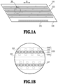
- FIG. 1 A is a plan view showing an element substrate
- FIG. 1 B is an enlarged view showing a portion IB in FIG. 1 A ;
- FIG. 2 A is a plan view of a heating element
- FIG. 2 B is a cross-sectional view taken along a line IIB-IIB in FIG. 2 A ;
- FIG. 3 A is a plan view of the element substrate
- FIG. 3 B is an enlarged view of an electrical wiring layer
- FIG. 4 A is a plan view of the element substrate
- FIG. 4 B is an enlarged view of the electrical wiring layer
- FIG. 5 is a diagram showing through holes between electrical wiring layers
- FIG. 6 A is a diagram illustrating wiring resistance
- FIG. 6 B is a diagram showing a simulation result of a voltage drop
- FIG. 6 C is a diagram showing a simulation result of a voltage drop
- FIG. 7 A is a plan view of the element substrate
- FIG. 7 B is an enlarged view of the electrical wiring layer
- FIG. 8 A is a plan view of the element substrate
- FIG. 8 B is an enlarged view of the electrical wiring layer
- FIG. 9 is a diagram showing a power supply wiring layer.
- FIG. 1 A is a plan view showing an element substrate 100 in the present embodiment and FIG. 1 B is an enlarged view showing a portion IB in FIG. 1 A .
- the element substrate 100 has a plane shape of a parallelogram and includes a plurality of heating elements 101 in a plurality of rows, a drive circuit 203 configured to drive each of the heating elements 101 , and an electrode pad 201 configured to transfer a driving current to the heating element 101 .
- the element substrate 100 includes an ejection port forming member 108 formed by aligning a plurality of ejection ports 109 provided in correspondence with the heating elements 101 in rows along an arrow S direction. In the print head, a plurality of the element substrates 100 are arranged in the arrow S direction.
- the drive circuit 203 is connected to an electrode pad 201 and generates a driving current for the heating element 101 according to a print signal supplied from the outside of the print head via the electrode pad 201 .
- a liquid supply path 301 and a liquid collection path 302 extend in the arrow S direction and the liquid supply path 301 and the liquid collection path 302 is provided with a plurality of openings 300 (a supply port 300 a , a collection port 300 b ), respectively.
- the liquid supply path 301 is provided with a plurality of the supply ports 300 a capable of supplying the heating elements 101 with a liquid
- the liquid collection path 302 is provided with a plurality of the collection ports 300 b capable of collecting the liquid from the heating elements 101 .
- the liquid supplied to a pressure chamber 107 from the supply port 300 a of the liquid supply path 301 is heated by the heating element 101 and foamed, so that the liquid is ejected from each of the ejection ports 109 .
- the liquid supplied from the supply port 300 a and not ejected is collected at the collection port 300 b in the liquid collection path 302 .
- the ink collected at the collection port 300 b is supplied to the liquid ejection head again via a tank unit (not shown) or the like provided in a printing apparatus. In this way, the liquid circulates in the printing apparatus.
- the supply port 300 a and the collection port 300 b are through holes that penetrate a substrate 114 in the element substrate 100 (see FIG. 2 B to be described later). As described above, by sandwiching the heating element 101 between the supply port 300 a and the collection port 300 b , refilling after ejection can be performed at a relatively high speed.
- FIG. 2 A is an enlarged plan view of a peripheral area of one heating element 101 in the element substrate of the print head of the present embodiment and FIG. 2 B is a cross-sectional view taken along a line IIB-IIB in FIG. 2 A .
- the heating element 101 is provided so as to face the ejection port 109 and is provided with a plurality of connecting members 102 connecting an electrical wiring line 103 and the heating element 101 .
- the direction of a current flowing through the heating element 101 is defined as an X direction and a direction orthogonal to the X direction is defined as a Y direction. Additionally, a direction orthogonal to the X direction and the Y direction is defined as a Z direction.
- the Y direction is a direction in which the heating elements 101 or the ejection ports 109 are arranged.
- the Z direction is a direction orthogonal to a surface on which the ejection port is formed and is a direction in which the liquid is ejected.
- the element substrate 100 includes the substrate 114 and the ejection port forming member 108 .
- the substrate 114 includes a base material 113 formed of Si and an insulating film 104 formed on the base material 113 .
- the heating element 101 that generates heat energy for ejecting a liquid, a protective film 105 , and a cavitation resistant film 106 are provided.
- the heating element 101 is formed of a Ta compound such as TaSiN.
- the insulating film 104 is formed of an insulator such as SiO.
- the ejection port forming member 108 is provided on the surface of the substrate 114 on which the heating element 101 is formed.
- the ejection port forming member 108 includes the ejection ports 109 corresponding to respective heating elements 101 and forms the pressure chamber 107 for each ejection port 109 together with the substrate 114 .
- the electrical wiring line 103 for supplying the heating element 101 with a current is provided so as to be embedded in the insulating film 104 .
- the electrical wiring line 103 electrically connects the drive circuit 203 and the heating element 101 via each of the connecting members 102 .
- the electrical wiring line 103 is made of aluminum and has a film thickness (a dimension in the Z direction) of about 0.4 to 1.2 ⁇ m.
- the heating element 101 generates heat due to the supplied current, and the heating element 101 having a high temperature heats the liquid in the pressure chamber 107 to generate bubbles. The bubbles cause the liquid in the vicinity of the ejection port 109 to be ejected from the ejection port 109 and printing is performed.
- the heating element 101 is covered with the protective film 105 made of SiN.
- the protective film 105 may be formed of SiO or SiC.
- the protective film 105 is covered with the cavitation resistant film 106 .
- the cavitation resistant film 106 is made of Ta or Ir.
- the electrical wiring line 103 is a metal and may be any one of Al, Cu, Ag, Au, Pt, W, Ni, and Co or an alloy including any one of Al, Cu, Ag, Au, Pt, W, Ni, and Co.
- the connecting members 102 are positioned at intervals along the Y direction. Each of the connecting members 102 is covered with the heating element 101 when viewed from a direction orthogonal to the surface on which the heating element 101 is provided.
- the connecting member 102 connects the electrical wiring line 103 and the heating element 101 in the vicinity of both end portions in the X direction of the heating element 101 . Accordingly, the current flows in the X direction in the heating element 101 .
- the heating element 101 includes, at one end side and the other end side, connection areas 110 to which a plurality of connecting members 102 are connected.
- the connecting member 102 is a plug extending in the Z direction from the vicinity of an end portion of the electrical wiring line 103 .
- the connecting member 102 has a substantially square cross section in the present embodiment, but corners may be rounded, and the shape of the cross section is not limited to a square but may be another shape such as a rectangle, a circle, or an ellipse.
- the connecting member 102 is made of tungsten but can be formed of any one of titanium, platinum, cobalt, nickel, molybdenum, tantalum, and silicon, or a compound thereof.
- the connecting member 102 may be integrally formed with the electrical wiring line 103 . That is, the connection member 102 integrated with the electrical wiring line 103 may be formed by cutting out a portion of the electrical wiring line 103 in a thickness direction.
- the electrical wiring line 103 is provided in the insulating film 104 and is connected to the heating element 101 via the connecting member 102 . Since electrical connection is made to the heating element 101 from a back surface side in this way, there is no need for an electrical wiring line covering the front surface side of the heating element 101 . In a configuration in which the electrical wiring line 103 is connected to the front surface side of the heating element 101 , an electrical wiring line having a film thickness of about 0.6 to 1.2 ⁇ m is laminated on the heating element 101 . Thus, there is a need to provide a protective film having a relatively large film thickness in order to secure a coverage property for a step height of about 0.6 to 1.2 ⁇ m.
- the electrical wiring line provided on the front surface side of the heating element 101 .
- the film thickness of the heating element 101 is about 0.01 to 0.05 ⁇ m, the step height is significantly smaller than that in the above configuration.
- a sufficient coverage property can be secured with the protective film 105 having a film thickness of about 0.15 to 0.3 ⁇ m, so that the protective film 105 can be thinned and the efficiency of heat transfer to ink is remarkably improved. This can achieve both reduction in power consumption and high quality by stabilizing foaming.
- a base (lower area) of the heating element 101 is preferably flat.
- the electrical wiring line 103 of each layer and the base portion of the heating element 101 are flattened by processing such as CMP.
- a contact surface of the connecting member 102 which is in contact with the heating element 101 and a contact surface of the insulating film 104 which is in contact with the heating element 101 are provided on the same plane.
- the base (lower area) of a heat generating resistor layer allows the electrical wiring line 103 of a pattern such as a signal wiring line and a power supply wiring line to pass immediately under the heating element 101 , that is, through the insulating film 104 between a central area 122 to be described later and the base material 113 or around the heating element 101 .
- a transistor can be arranged in the area, the area of the element substrate 100 can be reduced, the cost of the print head can be reduced, and the density of the ejection port 109 can be increased.
- the drive circuit 203 and a field oxide film 132 are formed in an interface area between the base material 113 formed of Si and the insulating film 104 .
- Such a configuration enables to multi-layer the electrical wiring line 103 while suppressing an influence on the characteristics of the heating element 101 . Further, allocating a plurality of wiring layers to the electrical wiring line 103 enables to significantly reduce power supply wiring resistance.
- the electrical wiring line 103 has three layers at different distances from the heating element 101 in a direction orthogonal to the plane of the element substrate 100 .
- the electrical wiring layer includes an electrical wiring layer 103 a farthest from the heating element 101 , an electrical wiring layer 103 b second farthest from the heating element 101 , and an electrical wiring layer 103 c closest to the heating element 101 .
- the electrical wiring layer 103 a is allocated to a signal wiring layer or a logic power supply wiring layer for driving the heating element 101 .
- the electrical wiring layer 103 b is allocated to the signal wiring layer or the logic power supply wiring layer for driving the heating element 101 and a wiring layer for supplying the heating element 101 with a current.
- the electrical wiring layer 103 c is allocated to a wiring layer for supplying the heating element 101 with a current.
- a VH wiring layer provided with a positive side (one side) wiring line for passing a current through a heating element and a GNDH wiring layer provided with a negative side (the other side) wiring line are provided so as to face each other.
- the VH wiring line and the GNDH wiring line face each other in a large area, there is a possibility that the frequency of interlayer short circuits caused by foreign matter will increase, and there is concern that yield decreases.
- each of the VH wiring line and the GNDH wiring line uses one layer, which costs.
- the VH wiring line and the GNDH wiring line are provided in the same layer. It is only required that at least a pair of the VH wiring line and GNDH wiring line be provided in parallel in the same layer. A detailed description will be given of the electrical wiring layer in the present embodiment.
- FIG. 3 A is a plan view showing the element substrate 100 and FIG. 3 B is an enlarged view of the electrical wiring layer 103 b in a portion IIIB in FIG. 3 A .
- the electrical wiring layer 103 b includes a signal wiring line (not shown) for driving the heating element 101 , a logic power supply wiring line (not shown), and a power supply wiring line (electrical wiring group) for supplying the heating element 101 with a current.
- the power supply wiring line for supplying the heating element 101 with a current includes a VH wiring line 103 b 1 , which is a power supply wiring line connected to the entrance side of the current flowing through the heating element 101 , and a GNDH wiring line 103 b 2 , which is a wiring line connected to the outlet side of the current flowing through the heating element 101 .
- the VH wiring line 103 b 1 and the GNDH wiring line 103 b 2 are arranged alternately in the X direction as shown in FIG. 3 B .
- a plurality of pairs of the VH wiring line 103 b 1 and GNDH wiring line 103 b 2 run across the entire area of the element substrate 100 .
- the power supply wiring line is connected along the oblique side of the outer shape of the element substrate 100 in a section L in the figure.
- FIG. 4 A is a plan view showing the element substrate 100 and FIG. 4 B is an enlarged view of the electrical wiring layer 103 c in a portion IVB in FIG. 4 A .
- the electrical wiring layer 103 c includes a power supply wiring line for supplying the heating element 101 with a current.
- the power supply wiring line for supplying the heating element 101 with a current includes a VH wiring line 103 c 1 , which is a power supply wiring line connected to the entrance side of the current flowing through the heating element 101 , and a GNDH wiring line 103 c 2 , which is a power supply wiring line connected to the outlet side of the current flowing through the heating element 101 .
- the VH wiring line 103 c 1 and the GNDH wiring line 103 c 2 are arranged alternately in the Y direction as shown in FIG. 4 B .
- a plurality of pairs of the VH wiring line 103 c 1 and GNDH wiring line 103 c 2 run across the entire area of the element substrate 100 .
- the VH wiring line 103 c 1 and the GNDH wiring line 103 c 2 are connected to the heating element 101 via the connecting member 102 .
- the VH wiring line 103 b 1 and the VH wiring line 103 c 1 are connected in different layers via a through-hole wiring line at a location where the wiring lines intersect and overlap each other in a case where the element substrate 100 is viewed from the front (when viewed from a viewpoint on a line perpendicular to the electrical wiring layer).
- the GNDH wiring line 103 b 2 and the GNDH wiring line 103 c 2 are also connected in different layers via a through-hole wiring line at a location where the wiring lines intersect and overlap each other in a case where the element substrate 100 is viewed from the front.
- FIG. 5 is a diagram showing a cross section taken along a line V-V in FIG. 4 B .
- a through hole 50 is formed between the VH wiring line 103 b 1 and the VH wiring line 103 c 1 .
- the VH wiring line 103 b 1 and the VH wiring line 103 c 1 are connected via the through-hole wiring line formed in the through hole.
- the connection between the VH wiring line 103 b 1 and the VH wiring line 103 c 1 has been described as an example here, but the same applies to the GNDH wiring line 103 b 2 and the GNDH wiring line 103 c 2 .
- the electrical wiring layer 103 c is routed in the X direction and the electrical wiring layer 103 b is routed in the Y direction.
- the thickness (wiring thickness) of the electrical wiring layer 103 c is 0.8 to 1.2 ⁇ m and the thickness of the electrical wiring layer 103 b is 0.3 to 0.6 ⁇ m.
- the electrical wiring layer 103 c has a film thickness larger than that of the electrical wiring layer 103 b .
- a voltage drop due to wiring resistance can be reduced by routing a wiring line with a large film thickness and a large cross-sectional area along a longitudinal direction (X direction) than by routing a wiring line with a large film thickness in a lateral direction (Y direction).
- the electrical wiring layer 103 c routed in the X direction which is the longitudinal direction has a film thickness larger than that of the electrical wiring layer 103 b routed in the Y direction to reduce the voltage drop.
- FIGS. 6 A, 6 B, and 6 C are diagrams illustrating wiring resistance from a heating element driving electrode 600 to the heating element 101 and showing results of simulating a voltage drop caused by the wiring resistance.
- a voltage drop in the case of driving simultaneously a total of four rows (rows A to D) of 32 heating elements 101 in one row is simulated.
- FIG. 6 B shows a simulation result of routing the electrical wiring layer 103 c with a large film thickness in the longitudinal direction (X direction) as in the present embodiment
- FIG. 6 C shows a simulation result of routing the electrical wiring layer 103 c in the lateral direction (Y direction).
- a voltage drop value is high in a position 601 (data number 0) and a position 604 (data number 32) where the heating element 101 farthest from the heating element driving electrode 600 is located.
- the VH wiring line and the GNDH wiring line are provided in the same layer. As a result, it is possible to reduce an area where the power supply wiring lines different between the layers face each other (only at locations where the power supply wiring lines intersect each other). This makes it possible to suppress the frequency of interlayer leakages caused by foreign matter generated at the time of generating a wiring line or the like and can achieve a reduction in yield in the manufacturing process. Further, since the VH wiring line and the GNDH wiring line are alternately routed in the same layer, wiring layer constituents can be reduced, so that an increase in cost can be suppressed.
- FIG. 7 A is a plan view showing the element substrate 100 in the present embodiment and FIG. 7 B is an enlarged view of the electrical wiring layer 103 b in a portion VIIB in FIG. 7 A .
- the element substrate 100 in the present embodiment has a rectangular outer shape as shown in FIG. 7 A . That is, since the outer shape of the element substrate 100 is a rectangle extending in the X direction and the Y direction, the power supply wiring line is connected along the Y direction in a section L in the figure, and the VH wiring line 103 b 1 and the GNDH wiring line 103 b 2 are arranged alternately in the X direction.
- FIG. 8 A is a plan view showing the element substrate 100 and FIG. 8 B is an enlarged view of the electrical wiring layer 103 c in a portion VIIIB in FIG. 8 A .
- the VH wiring line 103 c 1 and the GNDH wiring line 103 c 2 are alternately arranged in the Y direction as shown in FIG. 8 B .
- the VH wiring line 103 c 1 and the GNDH wiring line 103 c 2 are similarly run across the entire area of the element substrate 100 .
- a through hole is provided at a location where the power supply VH wiring line 103 b 1 and the VH wiring line 103 c 1 intersect and overlap each other.
- the power supply VH wiring line 103 b 1 and the VH wiring line 103 c 1 are connected via a through-hole wiring line.
- the GNDH wiring line 103 b 2 and the GNDH wiring line 103 c 2 are also provided with a through hole at a location where the GNDH wiring line 103 b 2 and the GNDH wiring line 103 c 2 intersect and overlap each other.
- the GNDH wiring line 103 b 2 and the GNDH wiring line 103 c 2 are connected via a through-hole wiring line.
- FIG. 9 is a diagram showing a power supply wiring layer in the present embodiment.
- the element substrate 100 of the present embodiment includes the electrical wiring layer 103 a farthest from the heating element 101 , the electrical wiring layer 103 b second farthest from the heating element 101 , the electrical wiring layer 103 c closer to the heating element 101 than the electrical wiring layer 103 b , and an electrical wiring layer 103 d closest to the heating element 101 .
- the electrical wiring layer 103 a , the electrical wiring layer 103 b , and the electrical wiring layer 103 c are the same as those in the first and second embodiments.
- the electrical wiring layer 103 d is an electrical wiring line having the same shape and the same arrangement (same configuration) as those of the electrical wiring layer 103 c .
- a through hole is provided between the VH wiring line 103 c 1 of the electrical wiring layer 103 c and the VH wiring line 103 d 1 of the electrical wiring layer 103 d .
- the VH wiring line 103 c 1 and the VH wiring line 103 d 1 are connected via a through-hole wiring line.
- a through hole is also provided between the GNDH wiring line 103 c 2 of the electrical wiring layer 103 c and the GNDH wiring line 103 d 2 of the electrical wiring layer 103 d .
- the GNDH wiring line 103 c 2 and the GNDH wiring line 103 d 2 are connected via a through-hole wiring line.
Landscapes
- Physics & Mathematics (AREA)
- Geometry (AREA)
- Particle Formation And Scattering Control In Inkjet Printers (AREA)
- Ink Jet (AREA)
Abstract
Description
Claims (11)
Applications Claiming Priority (2)
| Application Number | Priority Date | Filing Date | Title |
|---|---|---|---|
| JP2021-143903 | 2021-09-03 | ||
| JP2021143903A JP7786808B2 (en) | 2021-09-03 | 2021-09-03 | Element substrate and recording head |
Publications (2)
| Publication Number | Publication Date |
|---|---|
| US20230074434A1 US20230074434A1 (en) | 2023-03-09 |
| US12064965B2 true US12064965B2 (en) | 2024-08-20 |
Family
ID=85384866
Family Applications (1)
| Application Number | Title | Priority Date | Filing Date |
|---|---|---|---|
| US17/901,033 Active 2043-02-16 US12064965B2 (en) | 2021-09-03 | 2022-09-01 | Element substrate and print head |
Country Status (2)
| Country | Link |
|---|---|
| US (1) | US12064965B2 (en) |
| JP (1) | JP7786808B2 (en) |
Citations (5)
| Publication number | Priority date | Publication date | Assignee | Title |
|---|---|---|---|---|
| JP2004261985A (en) * | 2003-02-28 | 2004-09-24 | Sony Corp | Liquid ejection head, liquid ejection device, and method of driving liquid ejection head |
| US20150343773A1 (en) * | 2014-05-30 | 2015-12-03 | Canon Kabushiki Kaisha | Liquid ejection head |
| JP2016137705A (en) | 2015-01-27 | 2016-08-04 | キヤノン株式会社 | Element substrate for liquid discharge head and liquid discharge head |
| US10040284B2 (en) | 2015-07-02 | 2018-08-07 | Canon Kabushiki Kaisha | Discharge element substrate, printhead, and printing apparatus |
| US20190001680A1 (en) * | 2017-06-30 | 2019-01-03 | Canon Kabushiki Kaisha | Element board, liquid ejection head, and printing apparatus |
Family Cites Families (6)
| Publication number | Priority date | Publication date | Assignee | Title |
|---|---|---|---|---|
| JPH07297188A (en) * | 1994-04-25 | 1995-11-10 | Hitachi Ltd | Semiconductor integrated circuit device |
| JPH07312415A (en) * | 1994-05-16 | 1995-11-28 | Yamaha Corp | Semiconductor integrated circuit |
| JP2004296695A (en) * | 2003-03-26 | 2004-10-21 | Matsushita Electric Ind Co Ltd | Power supply wiring method and semiconductor device |
| JP2008105224A (en) * | 2006-10-24 | 2008-05-08 | Canon Inc | Inkjet recording substrate, recording head and recording apparatus provided with the substrate |
| JP2011213049A (en) * | 2010-04-01 | 2011-10-27 | Canon Inc | Liquid discharge head and driving method of the same |
| JP7397681B2 (en) * | 2020-01-16 | 2023-12-13 | キヤノン株式会社 | liquid discharge head |
-
2021
- 2021-09-03 JP JP2021143903A patent/JP7786808B2/en active Active
-
2022
- 2022-09-01 US US17/901,033 patent/US12064965B2/en active Active
Patent Citations (5)
| Publication number | Priority date | Publication date | Assignee | Title |
|---|---|---|---|---|
| JP2004261985A (en) * | 2003-02-28 | 2004-09-24 | Sony Corp | Liquid ejection head, liquid ejection device, and method of driving liquid ejection head |
| US20150343773A1 (en) * | 2014-05-30 | 2015-12-03 | Canon Kabushiki Kaisha | Liquid ejection head |
| JP2016137705A (en) | 2015-01-27 | 2016-08-04 | キヤノン株式会社 | Element substrate for liquid discharge head and liquid discharge head |
| US10040284B2 (en) | 2015-07-02 | 2018-08-07 | Canon Kabushiki Kaisha | Discharge element substrate, printhead, and printing apparatus |
| US20190001680A1 (en) * | 2017-06-30 | 2019-01-03 | Canon Kabushiki Kaisha | Element board, liquid ejection head, and printing apparatus |
Also Published As
| Publication number | Publication date |
|---|---|
| US20230074434A1 (en) | 2023-03-09 |
| JP7786808B2 (en) | 2025-12-16 |
| JP2023037261A (en) | 2023-03-15 |
Similar Documents
| Publication | Publication Date | Title |
|---|---|---|
| JP6598658B2 (en) | Element substrate for liquid discharge head and liquid discharge head | |
| CN101163591B (en) | Liquid discharge head, ink jet recording head and ink jet recording apparatus | |
| US10814623B2 (en) | Element substrate and liquid ejection head | |
| JP5197178B2 (en) | Inkjet recording head substrate and inkjet recording head | |
| CN109649012A (en) | Device substrate, the manufacturing method of device substrate, print head and printing equipment | |
| JP5436099B2 (en) | Method for manufacturing liquid discharge head substrate, liquid discharge head substrate, and liquid discharge head | |
| JP7471769B2 (en) | Element substrate, liquid ejection head and recording apparatus | |
| JP2009241438A (en) | Liquid droplet ejection head | |
| JP2011213049A (en) | Liquid discharge head and driving method of the same | |
| JP5208247B2 (en) | Inkjet recording head | |
| CN108859415B (en) | Printhead substrate, semiconductor substrate, manufacturing method thereof, and inkjet printing apparatus | |
| US7810907B2 (en) | Board for inkjet printing head and inkjet printing head using the same | |
| US12064965B2 (en) | Element substrate and print head | |
| US10889112B2 (en) | Liquid ejection head and manufacturing method thereof | |
| JP2019010769A (en) | Substrate for liquid discharge head and liquid discharge head | |
| US20260027836A1 (en) | Liquid ejection head substrate and liquid ejection head | |
| US20250196496A1 (en) | Element substrate and liquid ejection head | |
| US20250065625A1 (en) | Substrate for liquid ejection head, liquid ejection head, and method for manufacturing substrate for liquid ejection head | |
| CN110406258B (en) | Liquid ejection head substrate, method of manufacturing liquid ejection head substrate, and liquid ejection head | |
| JP2017094517A (en) | Actuator, inkjet head, and inkjet device | |
| CN120056598A (en) | Liquid ejecting head and method of manufacturing liquid ejecting head | |
| JP2016140977A (en) | Liquid ejection device and method of manufacturing liquid ejection device |
Legal Events
| Date | Code | Title | Description |
|---|---|---|---|
| FEPP | Fee payment procedure |
Free format text: ENTITY STATUS SET TO UNDISCOUNTED (ORIGINAL EVENT CODE: BIG.); ENTITY STATUS OF PATENT OWNER: LARGE ENTITY |
|
| AS | Assignment |
Owner name: CANON KABUSHIKI KAISHA, JAPAN Free format text: ASSIGNMENT OF ASSIGNORS INTEREST;ASSIGNORS:MIURA, YOSUKE;FUJII, YASUO;SOEDA, YASUHIRO;SIGNING DATES FROM 20220617 TO 20220620;REEL/FRAME:061341/0951 |
|
| STPP | Information on status: patent application and granting procedure in general |
Free format text: DOCKETED NEW CASE - READY FOR EXAMINATION |
|
| STPP | Information on status: patent application and granting procedure in general |
Free format text: NOTICE OF ALLOWANCE MAILED -- APPLICATION RECEIVED IN OFFICE OF PUBLICATIONS |
|
| ZAAA | Notice of allowance and fees due |
Free format text: ORIGINAL CODE: NOA |
|
| ZAAB | Notice of allowance mailed |
Free format text: ORIGINAL CODE: MN/=. |
|
| STPP | Information on status: patent application and granting procedure in general |
Free format text: PUBLICATIONS -- ISSUE FEE PAYMENT RECEIVED |
|
| STPP | Information on status: patent application and granting procedure in general |
Free format text: PUBLICATIONS -- ISSUE FEE PAYMENT VERIFIED |
|
| STCF | Information on status: patent grant |
Free format text: PATENTED CASE |