US12061493B2 - Low power hybrid reverse bandgap reference and digital temperature sensor - Google Patents
Low power hybrid reverse bandgap reference and digital temperature sensor Download PDFInfo
- Publication number
- US12061493B2 US12061493B2 US17/033,571 US202017033571A US12061493B2 US 12061493 B2 US12061493 B2 US 12061493B2 US 202017033571 A US202017033571 A US 202017033571A US 12061493 B2 US12061493 B2 US 12061493B2
- Authority
- US
- United States
- Prior art keywords
- transistor
- input
- size
- coupled
- amplifier
- Prior art date
- Legal status (The legal status is an assumption and is not a legal conclusion. Google has not performed a legal analysis and makes no representation as to the accuracy of the status listed.)
- Active, expires
Links
- 230000002441 reversible effect Effects 0.000 title abstract description 27
- 230000006870 function Effects 0.000 claims description 16
- 230000003071 parasitic effect Effects 0.000 abstract description 9
- 239000004065 semiconductor Substances 0.000 abstract description 5
- 238000012546 transfer Methods 0.000 abstract description 5
- 229910044991 metal oxide Inorganic materials 0.000 abstract description 4
- 150000004706 metal oxides Chemical class 0.000 abstract description 4
- 238000007726 management method Methods 0.000 description 18
- 238000000034 method Methods 0.000 description 18
- 230000008569 process Effects 0.000 description 14
- 238000012545 processing Methods 0.000 description 12
- 238000013461 design Methods 0.000 description 9
- 238000005516 engineering process Methods 0.000 description 9
- 230000000694 effects Effects 0.000 description 8
- 230000002093 peripheral effect Effects 0.000 description 8
- 238000005259 measurement Methods 0.000 description 7
- 238000004891 communication Methods 0.000 description 6
- 238000009529 body temperature measurement Methods 0.000 description 5
- 230000001413 cellular effect Effects 0.000 description 5
- 230000008859 change Effects 0.000 description 5
- 238000006243 chemical reaction Methods 0.000 description 5
- 238000010801 machine learning Methods 0.000 description 5
- 239000003990 capacitor Substances 0.000 description 4
- 238000010586 diagram Methods 0.000 description 3
- 239000002184 metal Substances 0.000 description 3
- 238000003032 molecular docking Methods 0.000 description 3
- 238000009966 trimming Methods 0.000 description 3
- XUIMIQQOPSSXEZ-UHFFFAOYSA-N Silicon Chemical compound [Si] XUIMIQQOPSSXEZ-UHFFFAOYSA-N 0.000 description 2
- 230000006399 behavior Effects 0.000 description 2
- 230000001419 dependent effect Effects 0.000 description 2
- 230000007613 environmental effect Effects 0.000 description 2
- 230000003993 interaction Effects 0.000 description 2
- 230000007774 longterm Effects 0.000 description 2
- 238000012986 modification Methods 0.000 description 2
- 230000004048 modification Effects 0.000 description 2
- 230000003287 optical effect Effects 0.000 description 2
- 229910052710 silicon Inorganic materials 0.000 description 2
- 239000010703 silicon Substances 0.000 description 2
- 238000003860 storage Methods 0.000 description 2
- 239000000758 substrate Substances 0.000 description 2
- 238000012360 testing method Methods 0.000 description 2
- 230000007704 transition Effects 0.000 description 2
- OKTJSMMVPCPJKN-UHFFFAOYSA-N Carbon Chemical compound [C] OKTJSMMVPCPJKN-UHFFFAOYSA-N 0.000 description 1
- 206010047289 Ventricular extrasystoles Diseases 0.000 description 1
- 230000004913 activation Effects 0.000 description 1
- 239000008186 active pharmaceutical agent Substances 0.000 description 1
- 230000003044 adaptive effect Effects 0.000 description 1
- 238000013459 approach Methods 0.000 description 1
- 230000003190 augmentative effect Effects 0.000 description 1
- 230000033228 biological regulation Effects 0.000 description 1
- 239000002041 carbon nanotube Substances 0.000 description 1
- 229910021393 carbon nanotube Inorganic materials 0.000 description 1
- 239000000969 carrier Substances 0.000 description 1
- 230000000295 complement effect Effects 0.000 description 1
- 238000004590 computer program Methods 0.000 description 1
- 239000000470 constituent Substances 0.000 description 1
- 230000008878 coupling Effects 0.000 description 1
- 238000010168 coupling process Methods 0.000 description 1
- 238000005859 coupling reaction Methods 0.000 description 1
- 230000007423 decrease Effects 0.000 description 1
- 238000001514 detection method Methods 0.000 description 1
- 239000013013 elastic material Substances 0.000 description 1
- 238000001914 filtration Methods 0.000 description 1
- 238000003384 imaging method Methods 0.000 description 1
- 238000004519 manufacturing process Methods 0.000 description 1
- 230000007246 mechanism Effects 0.000 description 1
- 238000010295 mobile communication Methods 0.000 description 1
- 238000005457 optimization Methods 0.000 description 1
- 238000004806 packaging method and process Methods 0.000 description 1
- 230000010363 phase shift Effects 0.000 description 1
- 229910021420 polycrystalline silicon Inorganic materials 0.000 description 1
- APTZNLHMIGJTEW-UHFFFAOYSA-N pyraflufen-ethyl Chemical compound C1=C(Cl)C(OCC(=O)OCC)=CC(C=2C(=C(OC(F)F)N(C)N=2)Cl)=C1F APTZNLHMIGJTEW-UHFFFAOYSA-N 0.000 description 1
- 230000004044 response Effects 0.000 description 1
- 230000004043 responsiveness Effects 0.000 description 1
- 238000009738 saturating Methods 0.000 description 1
- 238000012216 screening Methods 0.000 description 1
- 230000003068 static effect Effects 0.000 description 1
- CFMYXEVWODSLAX-QOZOJKKESA-N tetrodotoxin Chemical compound O([C@@]([C@H]1O)(O)O[C@H]2[C@@]3(O)CO)[C@H]3[C@@H](O)[C@]11[C@H]2[C@@H](O)N=C(N)N1 CFMYXEVWODSLAX-QOZOJKKESA-N 0.000 description 1
- 230000005641 tunneling Effects 0.000 description 1
- 230000000007 visual effect Effects 0.000 description 1
Images


Classifications
-
- G—PHYSICS
- G05—CONTROLLING; REGULATING
- G05F—SYSTEMS FOR REGULATING ELECTRIC OR MAGNETIC VARIABLES
- G05F1/00—Automatic systems in which deviations of an electric quantity from one or more predetermined values are detected at the output of the system and fed back to a device within the system to restore the detected quantity to its predetermined value or values, i.e. retroactive systems
- G05F1/10—Regulating voltage or current
- G05F1/46—Regulating voltage or current wherein the variable actually regulated by the final control device is DC
- G05F1/56—Regulating voltage or current wherein the variable actually regulated by the final control device is DC using semiconductor devices in series with the load as final control devices
- G05F1/565—Regulating voltage or current wherein the variable actually regulated by the final control device is DC using semiconductor devices in series with the load as final control devices sensing a condition of the system or its load in addition to means responsive to deviations in the output of the system, e.g. current, voltage, power factor
- G05F1/567—Regulating voltage or current wherein the variable actually regulated by the final control device is DC using semiconductor devices in series with the load as final control devices sensing a condition of the system or its load in addition to means responsive to deviations in the output of the system, e.g. current, voltage, power factor for temperature compensation
-
- G—PHYSICS
- G05—CONTROLLING; REGULATING
- G05F—SYSTEMS FOR REGULATING ELECTRIC OR MAGNETIC VARIABLES
- G05F3/00—Non-retroactive systems for regulating electric variables by using an uncontrolled element, or an uncontrolled combination of elements, such element or such combination having self-regulating properties
- G05F3/02—Regulating voltage or current
- G05F3/08—Regulating voltage or current wherein the variable is DC
- G05F3/10—Regulating voltage or current wherein the variable is DC using uncontrolled devices with non-linear characteristics
- G05F3/16—Regulating voltage or current wherein the variable is DC using uncontrolled devices with non-linear characteristics being semiconductor devices
- G05F3/20—Regulating voltage or current wherein the variable is DC using uncontrolled devices with non-linear characteristics being semiconductor devices using diode- transistor combinations
- G05F3/30—Regulators using the difference between the base-emitter voltages of two bipolar transistors operating at different current densities
Definitions
- BGR Bandgap reference
- DTS Digital Temperature Sensor
- FIG. 1 illustrates a low power hybrid reverse bandgap reference and digital temperature sensor, in accordance with some embodiments.
- FIG. 2 illustrates an unbalanced n-type input amplifier for the low power hybrid reverse bandgap reference and digital temperature sensor, in accordance with some embodiments.
- FIG. 3 illustrates an unbalanced p-type input amplifier for the low power hybrid reverse bandgap reference and digital temperature sensor, in accordance with some embodiments.
- FIGS. 4 A-B illustrate circuits to generate scaled emitter-base voltage for the low power hybrid reverse bandgap reference and digital temperature sensor, in accordance with some embodiments.
- FIG. 5 illustrates a plot showing the low power hybrid reverse bandgap reference operating as a digital temperature sensor, in accordance with some embodiments.
- FIGS. 6 A-B illustrates a layout of a bi-polar junction temperature device used in known bandgap circuits, and a layout of a single BJT device with a larger resistor ladder used in the low power hybrid reverse bandgap reference and digital temperature sensor, respectively, in accordance with some embodiments.
- FIG. 7 illustrates a smart device or a computer system or a SoC (System-on-Chip) with low power hybrid reverse bandgap reference and digital temperature sensor, respectively, in accordance with some embodiments.
- SoC System-on-Chip
- the temperature information can be obtained by comparing V BGR and V EB , so an analog-to-digital converter (ADC) is added to perform the comparison and thus implement the DTS function.
- ADC analog-to-digital converter
- the BJT device ends up using a relatively large footprint, especially in advanced semiconductor process.
- some client and server DTS designs leverage the existing sort and class test conditions to implement two-temperature (two-point) trimming which may not be viable in low cost test environments required by low BOM products.
- traditional BGREFs demand larger currents to bias a pair of BJTs and the matching of such structure is also a critical aspect.
- DTS low-power, low-cost DTS
- One kind utilizes a resistor to sense the temperature and obtains the temperature information from phase shifts caused by resistance changes in an RC filter or from current changes in a resistor bridge.
- their implementations require silicided poly-silicon resistors and the conversion speed is very slow (in the ms range).
- An existing low-power DTS structure requires one-temperature (one-point) trimming and utilizes a pair of NPN devices to generate the PTAT (proportional to absolute temperature) and CTAT (Complementary to absolute temperature) currents.
- the temperature information can be obtained by tuning a resistor digital-to-analog converter (DAC) to equalize the PTAT and CTAT currents.
- DAC digital-to-analog converter
- NPN devices are only available in a triple-well process and their availability in low-cost dual-well processes is limited, a variation uses a subthreshold MOS device and parasitic PNP BJT to obtain the PTAT and CTAT currents, respectively.
- both of these designs require a complex external readout circuit as they have a non-linear transfer curve of output code versus temperature. Furthermore, they operate in current mode, which increases design complexity and causes power consumption variations with the output code.
- LPHR low power hybrid reverse
- MOS metal oxide semiconductor
- PNP parasitic BJT PNP parasitic BJT device
- the LPHR architecture of various embodiments uses low-cost MOS transistors and the standard parasitic PNP device. Based on a reverse bandgap voltage, the LPHR can work as a configurable BGR. By comparing the configurable BGR with the scaled base-emitter voltage, the circuit can also perform as a DTS with a linear transfer function with single-temperature trim for high accuracy.
- the LPHR can be configured as a BGR or DTS (or digital thermometer) and comprises a first resistor (R 1 ); an amplifier having a first input (Vin ⁇ ) coupled to the first resistor, and a second input (Vin+) to receive a scaled emitter-base voltage ( ⁇ V EB ); and a second resistor (R 2 ) having variable resistance, wherein the second resistor is coupled to the first input and an output of the amplifier, wherein the output of the amplifier is a bandgap reference (V_BGR).
- the amplifier is an unbalanced amplifier having imbalanced input pair size or imbalanced biasing currents.
- the amplifier comprises a first input transistor (Q 0 ) having a first size; and a second input transistor (Q 1 ) having a second size, wherein the first size is ‘n’ times larger than the second size.
- the amplifier further comprises a current mirror coupled to the first input transistor and a second input transistor; and a current source coupled to the first input transistor and a second input transistor.
- the current mirror comprises a third transistor (Q 2 ) which is diode-connected and coupled to the first input transistor, wherein the third transistor has a third size; and a fourth transistor (Q 3 ) coupled to the third transistor and the second input transistor, wherein the fourth transistor has a fourth size, wherein the fourth size is ‘m’ times larger than the third size.
- the scaled emitter-base voltage is a first scaled emitter-base voltage
- the LPHR comprises a comparator to compare the output of the amplifier with a second scaled emitter-base voltage ( ⁇ V EB ).
- the second scaled emitter-base voltage is higher than the first scaled emitter-base voltage.
- the LPHR is coupled to a successive approximation logic to receive an output of the comparator and to generate a digital code (Dout), wherein the digital code changes according to the output of the comparator.
- the digital code is a first digital code
- the LPHR comprises a multiplexer to select one of the first digital code or a second digital code (Dext), wherein an output of the multiplexer is to adjust the variable resistance of the second resistor.
- the first digital code indicates a temperature of the LPHR.
- the LPHR comprises a circuitry to generate the first scaled emitter-base voltage and the second scaled emitter-base voltage.
- the circuitry comprises: a resistor divider; a current source coupled to the resistor divider; and a transistor coupled to the current source and the resistor divider, wherein the resistor divider has a first tap to provide the first scaled emitter-base voltage and a second tap to provide the second scaled emitter-base voltage.
- the transistor is one of a PNP BJT or a PMOS transistor.
- the LPHR can be used as temperature sensors in hot spots of a die. The same circuit can also be used as a reference voltage generator.
- the LPHR-DTS of various embodiments can achieve high accuracy with a single temperature trim across a 38% larger working temperature range, using 25% less power and requiring 23% shorter conversion time while providing a linear code to temperature transfer function, for example.
- the LPHR-BGR achieves better temperature independence and PSRR performance while consuming 0.15 ⁇ the power of the existing base BGR circuit.
- signals are represented with lines. Some lines may be thicker, to indicate more constituent signal paths, and/or have arrows at one or more ends, to indicate primary information flow direction. Such indications are not intended to be limiting. Rather, the lines are used in connection with one or more exemplary embodiments to facilitate easier understanding of a circuit or a logical unit. Any represented signal, as dictated by design needs or preferences, may actually comprise one or more signals that may travel in either direction and may be implemented with any suitable type of signal scheme.
- connection means a direct connection, such as electrical, mechanical, or magnetic connection between the things that are connected, without any intermediary devices.
- Coupled means a direct or indirect connection, such as a direct electrical, mechanical, or magnetic connection between the things that are connected or an indirect connection, through one or more passive or active intermediary devices.
- adjacent generally refers to a position of a thing being next to (e.g., immediately next to or close to with one or more things between them) or adjoining another thing (e.g., abutting it).
- circuit or “module” may refer to one or more passive and/or active components that are arranged to cooperate with one another to provide a desired function.
- signal may refer to at least one current signal, voltage signal, magnetic signal, or data/clock signal.
- the meaning of “a,” “an,” and “the” include plural references.
- the meaning of “in” includes “in” and “on.”
- analog signal is any continuous signal for which the time varying feature (variable) of the signal is a representation of some other time varying quantity, i.e., analogous to another time varying signal.
- digital signal is a physical signal that is a representation of a sequence of discrete values (a quantified discrete-time signal), for example of an arbitrary bit stream, or of a digitized (sampled and analog-to-digital converted) analog signal.
- scaling generally refers to converting a design (schematic and layout) from one process technology to another process technology and may be subsequently being reduced in layout area. In some cases, scaling also refers to upsizing a design from one process technology to another process technology and may be subsequently increasing layout area.
- scaling generally also refers to downsizing or upsizing layout and devices within the same technology node.
- scaling may also refer to adjusting (e.g., slowing down or speeding up—i.e. scaling down, or scaling up respectively) of a signal frequency relative to another parameter, for example, power supply level.
- phrases “A and/or B” and “A or B” mean (A), (B), or (A and B).
- phrase “A, B, and/or C” means (A), (B), (C), (A and B), (A and C), (B and C), or (A, B and C).
- the transistors in various circuits and logic blocks described here are metal oxide semiconductor (MOS) transistors or their derivatives, where the MOS transistors include drain, source, gate, and bulk terminals.
- the transistors and/or the MOS transistor derivatives also include Tri-Gate and FinFET transistors, Gate All Around Cylindrical Transistors, Tunneling FET (TFET), Square Wire, or Rectangular Ribbon Transistors, ferroelectric FET (FeFETs), or other devices implementing transistor functionality like carbon nanotubes or spintronic devices.
- MOSFET symmetrical source and drain terminals i.e., are identical terminals and are interchangeably used here.
- a TFET device on the other hand, has asymmetric Source and Drain terminals.
- BJT PNP/NPN Bi-polar junction transistors
- BiCMOS BiCMOS
- CMOS complementary metal oxide semiconductor
- FIG. 1 illustrates a low power hybrid reverse bandgap reference and digital temperature sensor 100 (herein LPHR circuit 100 ), in accordance with some embodiments.
- LPHR circuit 100 comprises unbalanced amplifier 101 , comparator 102 , Successive Approximation Register (SAR Logic) 103 , first scaled voltage source 104 , second scaled voltage source 105 , multiplexer (Mux) 106 , resistor R 1 , and resistor R 2 coupled as shown.
- SAR Logic Successive Approximation Register
- Mux multiplexer
- resistor R 1 resistor
- resistor R 2 resistor R 2 coupled as shown.
- Mux 106 is used to adjust the resistance of resistor R 2 via one of external data (D ext ) or data D out from SAR 103 .
- LPHR circuit 100 works as a configurable BGR if D ext is selected and as a DTS if D out is chosen. So, depending on whether LPHR circuit 100 is configured as a BGR or DTS, Mux 106 selects (using Select signal) one of D ext or D out . For example, when LPHR circuit 100 operates as BGR, Mux 106 selects D ext to select a resistance of R 2 to tune the bandgap reference voltage V_BGR, and selects D out when LPHR circuit 100 operates as a DTS.
- the output reference voltage V BGR can be adjusted with the input code D ext .
- the output V_BGR (or V BGR ) is compared with scaled ⁇ V EB by comparator 102 which generated the output Out for SAR 103 .
- amplifier 101 is an unbalanced amplifier working in weak inversion. Some embodiments of amplifier 101 are illustrated with reference to FIGS. 2 - 3 .
- FIG. 2 illustrates an unbalanced n-type input amplifier 200 for the low power hybrid reverse bandgap reference and digital temperature sensor, in accordance with some embodiments.
- Amplifier 200 comprises nMOS input transistors Q 0 and Q 1 , current mirror pMOS transistors Q 2 and Q 3 , and an n-type current source Qb biased by Vnbias.
- Input transistors receives Vin+ and Vin ⁇ signals, while output is provided on node Out.
- node names and signal names are interchangeably used.
- Out may refer to signal out or node out depending on the context of the sentence.
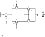
- FIG. 3 illustrates an unbalanced p-type input amplifier 300 for the low power hybrid reverse bandgap reference and digital temperature sensor, in accordance with some embodiments.
- Amplifier 300 is a flipped version of amplifier 200 .
- Amplifier 300 comprises pMOS input transistors Q 0 and Q 1 , current mirror nMOS transistors Q 2 and Q 3 , and an p-type current source Qb biased by Vpbias.
- Input transistors receives Vin+ and Vin ⁇ signals, while output is provided on node Out.
- the following section describes the basis of using unbalanced amplifier 200 or 300 for LPHR circuit 100 .
- the I DS to V GS characteristic is exponential, similar to the BJT:
- I DS I o ⁇ exp ⁇ ( V GS V T ) ( 2 )
- V T kT/q is the thermal voltage
- I o is a process related parameter but proportional to the transistor size (W/L). After some manipulation, it can be obtained:
- V GS V T ⁇ ln ⁇ ( I DS I o ) ( 3 )
- V GS difference is a function of the ratio of their size and the level of I DS .
- the input pair transistors Q 0 and Q 1 of amplifier 200 / 300 operate in weak inversion, and their size ratio is 1:n. Furthermore, their current is also imbalanced by a ratio of m:1 which is set by the current mirror devices Q 2 and Q 3 in the active loads.
- the transistors Q 0 and Q 1 of amplifier 200 / 300 can be kept in weak inversion region by low current biasing and large transistor sizes.
- FIGS. 4 A-B illustrate circuits 400 and 420 , respectively, to generate scaled emitter-base voltage for the low power hybrid reverse bandgap reference and digital temperature sensor, in accordance with some embodiments.
- the scaled base-emitter voltages ( ⁇ V EB ) and ( ⁇ V EB ) in FIG. 1 are generated by one of circuits 400 or 420 .
- Circuit 400 comprises current source Isrc, a resistor divider network comprising resistors R, and a PNP BJT device coupled as shown.
- a current source is applied to bias the PNP device, whose emitter-to-base voltage V EB is widely used in many BGR circuits to generate the CTAT voltage and has a negative TC (e.g., ⁇ 1.5 ⁇ 1.6 mV/° C.), where TC is the temperature coefficient.
- the scaled base-emitter voltages ( ⁇ V EB ) and ( ⁇ V EB ) are generated by the resistor ladder of resistors R.
- V bgs V ptat ⁇ V EB (5)
- the PTAT voltage (V ptat ) has a positive TC
- the CTAT voltage (V EB ) has a negative TC.
- V bgs reverse bandgap reference voltage
- the resistor feedback configuration is used to generate a BGR voltage with reasonable magnitude:
- V BGR ( 1 + R 2 R 1 ) ⁇ V bgs ( 6 )
- a configurable BGR voltage is generated, in accordance with various embodiments.
- circuit 420 can be used for generating the scaled V EB .
- a substrate is used to form the parasitic PNP, this PNP device can be replaced with a MOS device in sub-threshold as shown in circuit 420 FIG. 4 B .
- Circuit 420 comprises current source Isrc, a resistor divider network comprising resistors R, and a pMOS device coupled as shown.
- the scaled V EB is generated by replacing the PNP with pMOS device biasing in sub-threshold region.
- the resistors of various embodiments can be implemented as discrete resistors, resistors offered by the process technology node, transistors configured as resistors, or a combination of them.
- the bias voltage Vnbias and Vpbias can be generated by any suitable reference generator such as a voltage divider, resistor divider, current mirror based reference generator, an internal on-die reference generator, an off-die reference generator, or a combination of them.
- FIG. 5 illustrates plot 500 showing the low power hybrid reverse bandgap reference operating as a digital temperature sensor, in accordance with some embodiments.
- Mux 106 selects Dout to adjust resistance R 2
- LPHR 100 operates as a DTS to obtain the temperature information by comparing the scaled V EB voltage and the BGR voltage V BGR . Its function and circuit implementation are illustrated as follows.
- V BGR increases linearly with R 2 .
- different bandgap voltages can be obtained such as V BGR(1) and V BGR(2) as shown in plot 500 , and they are invariant with temperature.
- the V EB is a CTAT voltage with negative TC, so the temperature information can be obtained by comparing the V EB and V BGR .
- LPHR 100 significantly increases the working temperature range because it avoids the current comparator saturation problem existing temperature sensor circuits. Note, that the ⁇ V EB may be too small for use in this comparison by comparator 102 , so the other scaled CTAT voltage( ⁇ V EB ) is used to compare V BGR with ⁇ V EB , in accordance with some embodiments.
- the temperature information can be obtained from the value of R 2 (D out ) as,
- V go is approximately 1.2V, related to the silicon bandgap; tc is the TC of PNP devices.
- the D out codes are selected to control the tunable R 2 , and comparator 102 and digital Successive Approximation (SAR) logic circuits 103 are added as shown in FIG. 1 .
- SAR logic 103 generates an initial code D out which results in a V BGR(i) that is compared with ⁇ V EB .
- SAR logic 103 can automatically adjust the D out codes and after a number of clock cycles dictated by the required resolution, the final D out that ensures the V BGR(i) is equal to ⁇ V EB is obtained (as given by equation (7)).
- FIGS. 6 A-B illustrates layout 600 of a bi-polar junction temperature device used in known bandgap circuits, and layout 620 of a single BJT device with a larger resistor ladder used in the low power hybrid reverse bandgap reference and digital temperature sensor, respectively, in accordance with some embodiments.
- FIG. 6 A Most existing BGR/DTS circuits use a pair of BJT devices with size ratio of 1:8 to generate the required VEB voltages, and their layout structure is shown in FIG. 6 A .
- layout 600 one BJT is in the center and the other BJT is placed around to have a better matching performance.
- BJT 1 is in the center and BJT 2 are placed around it.
- a combination of a single BJT device with a large resistor ladder to generate the scaled VEB is a feature structure LPHR 100 .
- Its layout structure is shown as in FIG. 6 B , where a single BJT device, a large resistor array, switches (“SW”) and a current source (“CS”) generate the scaled VEBs.
- Circuit 100 and associated layout structure 620 provides an optimized layout which is less prone to BJT mismatch errors and lower power than the existing BGR/DTS designs.
- FIG. 7 illustrates a smart device or a computer system or a SoC (System-on-Chip) with low power hybrid reverse bandgap reference and digital temperature sensor, respectively, in accordance with some embodiments.
- device 2400 represents an appropriate computing device, such as a computing tablet, a mobile phone or smart-phone, a laptop, a desktop, an Internet-of-Things (IOT) device, a server, a wearable device, a set-top box, a wireless-enabled e-reader, or the like. It will be understood that certain components are shown generally, and not all components of such a device are shown in device 2400 .
- IOT Internet-of-Things
- the device 2400 comprises an SoC (System-on-Chip) 2401 .
- SoC System-on-Chip
- An example boundary of the SoC 2401 is illustrated using dotted lines in FIG. 7 , with some example components being illustrated to be included within SoC 2401 —however, SoC 2401 may include any appropriate components of device 2400 .
- device 2400 includes processor 2404 .
- Processor 2404 can include one or more physical devices, such as microprocessors, application processors, microcontrollers, programmable logic devices, processing cores, or other processing means.
- the processing operations performed by processor 2404 include the execution of an operating platform or operating system on which applications and/or device functions are executed.
- the processing operations include operations related to I/O (input/output) with a human user or with other devices, operations related to power management, operations related to connecting computing device 2400 to another device, and/or the like.
- the processing operations may also include operations related to audio I/O and/or display I/O.
- processor 2404 includes multiple processing cores (also referred to as cores) 2408 a , 2408 b , 2408 c . Although merely three cores 2408 a , 2408 b , 2408 c are illustrated in FIG. 7 , processor 2404 may include any other appropriate number of processing cores, e.g., tens, or even hundreds of processing cores. Processor cores 2408 a , 2408 b , 2408 c may be implemented on a single integrated circuit (IC) chip. Moreover, the chip may include one or more shared and/or private caches, buses or interconnections, graphics and/or memory controllers, or other components.
- IC integrated circuit
- processor 2404 includes cache 2406 .
- sections of cache 2406 may be dedicated to individual cores 2408 (e.g., a first section of cache 2406 dedicated to core 2408 a , a second section of cache 2406 dedicated to core 2408 b , and so on).
- one or more sections of cache 2406 may be shared among two or more of cores 2408 .
- Cache 2406 may be split in different levels, e.g., level 1 (L1) cache, level 2 (L2) cache, level 3 (L3) cache, etc.
- processor core 2404 may include a fetch unit to fetch instructions (including instructions with conditional branches) for execution by the core 2404 .
- the instructions may be fetched from any storage devices such as the memory 2430 .
- Processor core 2404 may also include a decode unit to decode the fetched instruction.
- the decode unit may decode the fetched instruction into a plurality of micro-operations.
- Processor core 2404 may include a schedule unit to perform various operations associated with storing decoded instructions.
- the schedule unit may hold data from the decode unit until the instructions are ready for dispatch, e.g., until all source values of a decoded instruction become available.
- the schedule unit may schedule and/or issue (or dispatch) decoded instructions to an execution unit for execution.
- the execution unit may execute the dispatched instructions after they are decoded (e.g., by the decode unit) and dispatched (e.g., by the schedule unit).
- the execution unit may include more than one execution unit (such as an imaging computational unit, a graphics computational unit, a general-purpose computational unit, etc.).
- the execution unit may also perform various arithmetic operations such as addition, subtraction, multiplication, and/or division, and may include one or more an arithmetic logic units (ALUs).
- ALUs arithmetic logic units
- a co-processor (not shown) may perform various arithmetic operations in conjunction with the execution unit.
- processor core 2404 may be an out-of-order processor core in one embodiment.
- Processor core 2404 may also include a retirement unit.
- the retirement unit may retire executed instructions after they are committed. In an embodiment, retirement of the executed instructions may result in processor state being committed from the execution of the instructions, physical registers used by the instructions being de-allocated, etc.
- Processor core 2404 may also include a bus unit to enable communication between components of processor core 2404 and other components via one or more buses.
- Processor core 2404 may also include one or more registers to store data accessed by various components of the core 2404 (such as values related to assigned app priorities and/or sub-system states (modes) association.
- device 2400 comprises connectivity circuitries 2431 .
- connectivity circuitries 2431 includes hardware devices (e.g., wireless and/or wired connectors and communication hardware) and/or software components (e.g., drivers, protocol stacks), e.g., to enable device 2400 to communicate with external devices.
- Device 2400 may be separate from the external devices, such as other computing devices, wireless access points or base stations, etc.
- connectivity circuitries 2431 may include multiple different types of connectivity.
- the connectivity circuitries 2431 may include cellular connectivity circuitries, wireless connectivity circuitries, etc.
- Cellular connectivity circuitries of connectivity circuitries 2431 refers generally to cellular network connectivity provided by wireless carriers, such as provided via GSM (global system for mobile communications) or variations or derivatives, CDMA (code division multiple access) or variations or derivatives, TDM (time division multiplexing) or variations or derivatives, 3rd Generation Partnership Project (3GPP) Universal Mobile Telecommunications Systems (UMTS) system or variations or derivatives, 3GPP Long-Term Evolution (LTE) system or variations or derivatives, 3GPP LTE-Advanced (LTE-A) system or variations or derivatives, Fifth Generation (5G) wireless system or variations or derivatives, 5G mobile networks system or variations or derivatives, 5G New Radio (NR) system or variations or derivatives, or other cellular service standards.
- GSM global system for mobile communications
- CDMA code division multiple access
- TDM time division multiplexing
- 3GPP
- Wireless connectivity circuitries (or wireless interface) of the connectivity circuitries 2431 refers to wireless connectivity that is not cellular, and can include personal area networks (such as Bluetooth, Near Field, etc.), local area networks (such as Wi-Fi), and/or wide area networks (such as WiMax), and/or other wireless communication.
- connectivity circuitries 2431 may include a network interface, such as a wired or wireless interface, e.g., so that a system embodiment may be incorporated into a wireless device, for example, a cell phone or personal digital assistant.
- device 2400 comprises control hub 2432 , which represents hardware devices and/or software components related to interaction with one or more I/O devices.
- processor 2404 may communicate with one or more of display 2422 , one or more peripheral devices 2424 , storage devices 2428 , one or more other external devices 2429 , etc., via control hub 2432 .
- Control hub 2432 may be a chipset, a Platform Control Hub (PCH), and/or the like.
- PCH Platform Control Hub
- control hub 2432 illustrates one or more connection points for additional devices that connect to device 2400 , e.g., through which a user might interact with the system.
- devices e.g., devices 2429
- devices that can be attached to device 2400 include microphone devices, speaker or stereo systems, audio devices, video systems or other display devices, keyboard or keypad devices, or other I/O devices for use with specific applications such as card readers or other devices.
- control hub 2432 can interact with audio devices, display 2422 , etc.
- input through a microphone or other audio device can provide input or commands for one or more applications or functions of device 2400 .
- audio output can be provided instead of, or in addition to display output.
- display 2422 includes a touch screen
- display 2422 also acts as an input device, which can be at least partially managed by control hub 2432 .
- control hub 2432 manages devices such as accelerometers, cameras, light sensors or other environmental sensors, or other hardware that can be included in device 2400 .
- the input can be part of direct user interaction, as well as providing environmental input to the system to influence its operations (such as filtering for noise, adjusting displays for brightness detection, applying a flash for a camera, or other features).
- control hub 2432 may couple to various devices using any appropriate communication protocol, e.g., PCIe (Peripheral Component Interconnect Express), USB (Universal Serial Bus), Thunderbolt, High Definition Multimedia Interface (HDMI), Firewire, etc.
- PCIe Peripheral Component Interconnect Express
- USB Universal Serial Bus
- Thunderbolt Thunderbolt
- HDMI High Definition Multimedia Interface
- Firewire etc.
- display 2422 represents hardware (e.g., display devices) and software (e.g., drivers) components that provide a visual and/or tactile display for a user to interact with device 2400 .
- Display 2422 may include a display interface, a display screen, and/or hardware device used to provide a display to a user.
- display 2422 includes a touch screen (or touch pad) device that provides both output and input to a user.
- display 2422 may communicate directly with the processor 2404 .
- Display 2422 can be one or more of an internal display device, as in a mobile electronic device or a laptop device or an external display device attached via a display interface (e.g., DisplayPort, etc.).
- display 2422 can be a head mounted display (HMD) such as a stereoscopic display device for use in virtual reality (VR) applications or augmented reality (AR) applications.
- HMD head mounted display
- VR virtual reality
- AR augmented reality
- device 2400 may include Graphics Processing Unit (GPU) comprising one or more graphics processing cores, which may control one or more aspects of displaying contents on display 2422 .
- GPU Graphics Processing Unit
- Control hub 2432 may include hardware interfaces and connectors, as well as software components (e.g., drivers, protocol stacks) to make peripheral connections, e.g., to peripheral devices 2424 .
- software components e.g., drivers, protocol stacks
- device 2400 could both be a peripheral device to other computing devices, as well as have peripheral devices connected to it.
- Device 2400 may have a “docking” connector to connect to other computing devices for purposes such as managing (e.g., downloading and/or uploading, changing, synchronizing) content on device 2400 .
- a docking connector can allow device 2400 to connect to certain peripherals that allow computing device 2400 to control content output, for example, to audiovisual or other systems.
- device 2400 can make peripheral connections via common or standards-based connectors.
- Common types can include a Universal Serial Bus (USB) connector (which can include any of a number of different hardware interfaces), DisplayPort including MiniDisplayPort (MDP), High Definition Multimedia Interface (HDMI), Firewire, or other types.
- USB Universal Serial Bus
- MDP MiniDisplayPort
- HDMI High Definition Multimedia Interface
- Firewire or other types.
- connectivity circuitries 2431 may be coupled to control hub 2432 , e.g., in addition to, or instead of, being coupled directly to the processor 2404 .
- display 2422 may be coupled to control hub 2432 , e.g., in addition to, or instead of, being coupled directly to processor 2404 .
- device 2400 comprises memory 2430 coupled to processor 2404 via memory interface 2434 .
- Memory 2430 includes memory devices for storing information in device 2400 .
- memory 2430 includes apparatus to maintain stable clocking as described with reference to various embodiments.
- Memory can include nonvolatile (state does not change if power to the memory device is interrupted) and/or volatile (state is indeterminate if power to the memory device is interrupted) memory devices.
- Memory device 2430 can be a dynamic random-access memory (DRAM) device, a static random-access memory (SRAM) device, flash memory device, phase-change memory device, or some other memory device having suitable performance to serve as process memory.
- DRAM dynamic random-access memory
- SRAM static random-access memory
- flash memory device phase-change memory device, or some other memory device having suitable performance to serve as process memory.
- memory 2430 can operate as system memory for device 2400 , to store data and instructions for use when the one or more processors 2404 executes an application or process.
- Memory 2430 can store application data, user data, music, photos, documents, or other data, as well as system data (whether long-term or temporary) related to the execution of the applications and functions of device 2
- Elements of various embodiments and examples are also provided as a machine-readable medium (e.g., memory 2430 ) for storing the computer-executable instructions (e.g., instructions to implement any other processes discussed herein).
- the machine-readable medium e.g., memory 2430
- embodiments of the disclosure may be downloaded as a computer program (e.g., BIOS) which may be transferred from a remote computer (e.g., a server) to a requesting computer (e.g., a client) by way of data signals via a communication link (e.g., a modem or network connection).
- BIOS a computer program
- a remote computer e.g., a server
- a requesting computer e.g., a client
- a communication link e.g., a modem or network connection
- device 2400 comprises temperature measurement circuitries 2440 , e.g., for measuring temperature of various components of device 2400 .
- temperature measurement circuitries 2440 may be embedded, or coupled or attached to various components, whose temperature are to be measured and monitored.
- temperature measurement circuitries 2440 may measure temperature of (or within) one or more of cores 2408 a , 2408 b , 2408 c , voltage regulator 2414 , memory 2430 , a mother-board of SoC 2401 , and/or any appropriate component of device 2400 .
- temperature measurement circuitries 2440 include a low power hybrid reverse (LPHR) bandgap reference (BGR) and digital temperature sensor (DTS), which utilizes subthreshold metal oxide semiconductor (MOS) transistor and the PNP parasitic Bi-polar Junction Transistor (BJT) device to form a reverse BGR that serves as the base for configurable BGR or DTS operating modes.
- the LPHR architecture uses low-cost MOS transistors and the standard parasitic PNP device. Based on a reverse bandgap voltage, the LPHR can work as a configurable BGR. By comparing the configurable BGR with the scaled base-emitter voltage, the circuit can also perform as a DTS with a linear transfer function with single-temperature trim for high accuracy.
- device 2400 comprises power measurement circuitries 2442 , e.g., for measuring power consumed by one or more components of the device 2400 .
- the power measurement circuitries 2442 may measure voltage and/or current.
- the power measurement circuitries 2442 may be embedded, or coupled or attached to various components, whose power, voltage, and/or current consumption are to be measured and monitored.
- power measurement circuitries 2442 may measure power, current and/or voltage supplied by one or more voltage regulators 2414 , power supplied to SoC 2401 , power supplied to device 2400 , power consumed by processor 2404 (or any other component) of device 2400 , etc.
- device 2400 comprises one or more voltage regulator circuitries, generally referred to as voltage regulator (VR) 2414 .
- VR 2414 generates signals at appropriate voltage levels, which may be supplied to operate any appropriate components of the device 2400 .
- VR 2414 is illustrated to be supplying signals to processor 2404 of device 2400 .
- VR 2414 receives one or more Voltage Identification (VID) signals, and generates the voltage signal at an appropriate level, based on the VID signals.
- VID Voltage Identification
- Various type of VRs may be utilized for the VR 2414 .
- VR 2414 may include a “buck” VR, “boost” VR, a combination of buck and boost VRs, low dropout (LDO) regulators, switching DC-DC regulators, constant-on-time controller-based DC-DC regulator, etc.
- Buck VR is generally used in power delivery applications in which an input voltage needs to be transformed to an output voltage in a ratio that is smaller than unity.
- Boost VR is generally used in power delivery applications in which an input voltage needs to be transformed to an output voltage in a ratio that is larger than unity.
- each processor core has its own VR, which is controlled by PCU 2410 a/b and/or PMIC 2412 .
- each core has a network of distributed LDOs to provide efficient control for power management.
- the LDOs can be digital, analog, or a combination of digital or analog LDOs.
- VR 2414 includes current tracking apparatus to measure current through power supply rail(s).
- VR 2414 includes a digital control scheme to manage states of a proportional-integral-derivative (PID) filter (also known as a digital Type-III compensator).
- PID proportional-integral-derivative
- the digital control scheme controls the integrator of the PID filter to implement non-linear control of saturating the duty cycle during which the proportional and derivative terms of the PID are set to 0 while the integrator and its internal states (previous values or memory) is set to a duty cycle that is the sum of the current nominal duty cycle plus a deltaD.
- the deltaD is the maximum duty cycle increment that is used to regulate a voltage regulator from ICCmin to ICCmax and is a configuration register that can be set post silicon.
- a state machine moves from a non-linear all ON state (which brings the output voltage Vout back to a regulation window) to an open loop duty cycle which maintains the output voltage slightly higher than the required reference voltage Vref. After a certain period in this state of open loop at the commanded duty cycle, the state machine then ramps down the open loop duty cycle value until the output voltage is close to the Vref commanded.
- output chatter on the output supply from VR 2414 is completely eliminated (or substantially eliminated) and there is merely a single undershoot transition which could lead to a guaranteed Vmin based on a comparator delay and the di/dt of the load with the available output decoupling capacitance.
- device 2400 comprises one or more clock generator circuitries, generally referred to as clock generator 2416 .
- Clock generator 2416 generates clock signals at appropriate frequency levels, which may be supplied to any appropriate components of device 2400 .
- clock generator 2416 is illustrated to be supplying clock signals to processor 2404 of device 2400 .
- clock generator 2416 receives one or more Frequency Identification (FID) signals, and generates the clock signals at an appropriate frequency, based on the FID signals.
- FID Frequency Identification
- device 2400 comprises battery 2418 supplying power to various components of device 2400 .
- battery 2418 is illustrated to be supplying power to processor 2404 .
- device 2400 may comprise a charging circuitry, e.g., to recharge the battery, based on Alternating Current (AC) power supply received from an AC adapter.
- battery 2418 includes battery subsystem which comprises battery control and driver MOS (DrMOS) block.
- the charging circuitry (e.g., 2418 ) comprises a buck-boost converter.
- This buck-boost converter comprises DrMOS or DrGaN devices used in place of half-bridges for traditional buck-boost converters.
- DrMOS Various embodiments here are described with reference to DrMOS. However, the embodiments are applicable to DrGaN.
- the DrMOS devices allow for better efficiency in power conversion due to reduced parasitic and optimized MOSFET packaging. Since the dead-time management is internal to the DrMOS, the dead-time management is more accurate than for traditional buck-boost converters leading to higher efficiency in conversion.
- the buck-boost converter of various embodiments comprises dual-folded bootstrap for DrMOS devices.
- folded bootstrap capacitors are added that cross-couple inductor nodes to the two sets of DrMOS switches.
- device 2400 comprises Power Control Unit (PCU) 2410 (also referred to as Power Management Unit (PMU), Power Controller, etc.).
- PCU Power Control Unit
- PMU Power Management Unit
- some sections of PCU 2410 may be implemented by one or more processing cores 2408 , and these sections of PCU 2410 are symbolically illustrated using a dotted box and labelled PCU 2410 a .
- some other sections of PCU 2410 may be implemented outside the processing cores 2408 , and these sections of PCU 2410 are symbolically illustrated using a dotted box and labelled as PCU 2410 b .
- PCU 2410 may implement various power management operations for device 2400 .
- PCU 2410 may include hardware interfaces, hardware circuitries, connectors, registers, etc., as well as software components (e.g., drivers, protocol stacks), to implement various power management operations for device 2400 .
- device 2400 comprises Power Management Integrated Circuit (PMIC) 2412 , e.g., to implement various power management operations for device 2400 .
- PMIC 2412 is a Reconfigurable Power Management ICs (RPMICs) and/or an IMVP (Intel® Mobile Voltage Positioning).
- RPMICs Reconfigurable Power Management ICs
- IMVP Intelligent Mobile Voltage Positioning
- the PMIC is within an IC chip separate from processor 2404 .
- The may implement various power management operations for device 2400 .
- PMIC 2412 may include hardware interfaces, hardware circuitries, connectors, registers, etc., as well as software components (e.g., drivers, protocol stacks), to implement various power management operations for device 2400 .
- device 2400 comprises one or both PCU 2410 or PMIC 2412 .
- any one of PCU 2410 or PMIC 2412 may be absent in device 2400 , and hence, these components are illustrated using dotted lines.
- Various power management operations of device 2400 may be performed by PCU 2410 , by PMIC 2412 , or by a combination of PCU 2410 and PMIC 2412 .
- PCU 2410 and/or PMIC 2412 may select a power state (e.g., P-state) for various components of device 2400 .
- PCU 2410 and/or PMIC 2412 may select a power state (e.g., in accordance with the ACPI (Advanced Configuration and Power Interface) specification) for various components of device 2400 .
- ACPI Advanced Configuration and Power Interface
- PCU 2410 and/or PMIC 2412 may cause various components of the device 2400 to transition to a sleep state, to an active state, to an appropriate C state (e.g., CO state, or another appropriate C state, in accordance with the ACPI specification), etc.
- PCU 2410 and/or PMIC 2412 may control a voltage output by VR 2414 and/or a frequency of a clock signal output by the clock generator, e.g., by outputting the VID signal and/or the FID signal, respectively.
- PCU 2410 and/or PMIC 2412 may control battery power usage, charging of battery 2418 , and features related to power saving operation.
- the clock generator 2416 can comprise a phase locked loop (PLL), frequency locked loop (FLL), or any suitable clock source.
- each core of processor 2404 has its own clock source. As such, each core can operate at a frequency independent of the frequency of operation of the other core.
- PCU 2410 and/or PMIC 2412 performs adaptive or dynamic frequency scaling or adjustment. For example, clock frequency of a processor core can be increased if the core is not operating at its maximum power consumption threshold or limit.
- PCU 2410 and/or PMIC 2412 determines the operating condition of each core of a processor, and opportunistically adjusts frequency and/or power supply voltage of that core without the core clocking source (e.g., PLL of that core) losing lock when the PCU 2410 and/or PMIC 2412 determines that the core is operating below a target performance level. For example, if a core is drawing current from a power supply rail less than a total current allocated for that core or processor 2404 , then PCU 2410 and/or PMIC 2412 can temporality increase the power draw for that core or processor 2404 (e.g., by increasing clock frequency and/or power supply voltage level) so that the core or processor 2404 can perform at higher performance level. As such, voltage and/or frequency can be increased temporality for processor 2404 without violating product reliability.
- the core clocking source e.g., PLL of that core
- PCU 2410 and/or PMIC 2412 may perform power management operations, e.g., based at least in part on receiving measurements from power measurement circuitries 2442 , temperature measurement circuitries 2440 , charge level of battery 2418 , and/or any other appropriate information that may be used for power management.
- PMIC 2412 is communicatively coupled to one or more sensors to sense/detect various values/variations in one or more factors having an effect on power/thermal behavior of the system/platform. Examples of the one or more factors include electrical current, voltage droop, temperature, operating frequency, operating voltage, power consumption, inter-core communication activity, etc.
- sensors may be provided in physical proximity (and/or thermal contact/coupling) with one or more components or logic/IP blocks of a computing system. Additionally, sensor(s) may be directly coupled to PCU 2410 and/or PMIC 2412 in at least one embodiment to allow PCU 2410 and/or PMIC 2412 to manage processor core energy at least in part based on value(s) detected by one or more of the sensors.
- processors 2404 may execute application programs 2450 , Operating System 2452 , one or more Power Management (PM) specific application programs (e.g., generically referred to as PM applications 2458 ), and/or the like. PM applications 2458 may also be executed by the PCU 2410 and/or PMIC 2412 .
- OS 2452 may also include one or more PM applications 2456 a , 2456 b , 2456 c .
- the OS 2452 may also include various drivers 2454 a , 2454 b , 2454 c , etc., some of which may be specific for power management purposes.
- device 2400 may further comprise a Basic Input/output System (BIOS) 2420 . BIOS 2420 may communicate with OS 2452 (e.g., via one or more drivers 2454 ), communicate with processors 2404 , etc.
- BIOS Basic Input/output System
- PM applications 2458 , 2456 , drivers 2454 , BIOS 2420 , etc. may be used to implement power management specific tasks, e.g., to control voltage and/or frequency of various components of device 2400 , to control wake-up state, sleep state, and/or any other appropriate power state of various components of device 2400 , control battery power usage, charging of the battery 2418 , features related to power saving operation, etc.
- battery 2418 is a Li-metal battery with a pressure chamber to allow uniform pressure on a battery.
- the pressure chamber is supported by metal plates (such as pressure equalization plate) used to give uniform pressure to the battery.
- the pressure chamber may include pressured gas, elastic material, spring plate, etc.
- the outer skin of the pressure chamber is free to bow, restrained at its edges by (metal) skin, but still exerts a uniform pressure on the plate that is compressing the battery cell.
- the pressure chamber gives uniform pressure to battery, which is used to enable high-energy density battery with, for example, 20% more battery life.
- pCode executing on PCU 2410 a/b has a capability to enable extra compute and telemetries resources for the runtime support of the pCode.
- pCode refers to a firmware executed by PCU 2410 a/b to manage performance of SoC 2401 .
- pCode may set frequencies and appropriate voltages for the processor.
- Part of the pCode are accessible via OS 2452 .
- mechanisms and methods are provided that dynamically change an Energy Performance Preference (EPP) value based on workloads, user behavior, and/or system conditions.
- EPP Energy Performance Preference
- an EPP parameter may inform a pCode algorithm as to whether performance or battery life is more important.
- This support may be done as well by OS 2452 by including machine-learning support as part of OS 2452 and either tuning the EPP value that the OS hints to the hardware (e.g., various components of SoC 2401 ) by machine-learning prediction, or by delivering the machine-learning prediction to the pCode in a manner similar to that done by a Dynamic Tuning Technology (DTT) driver.
- OS 2452 may have visibility to the same set of telemetries as are available to a DTT.
- pCode may tune its internal algorithms to achieve optimal power and performance results following the machine-learning prediction of activation type.
- the pCode as example may increase the responsibility for the processor utilization change to enable fast response for user activity, or may increase the bias for energy saving either by reducing the responsibility for the processor utilization or by saving more power and increasing the performance lost by tuning the energy saving optimization. This approach may facilitate saving more battery life in case the types of activities enabled lose some performance level over what the system can enable.
- the pCode may include an algorithm for dynamic EPP that may take the two inputs, one from OS 2452 and the other from software such as DTT, and may selectively choose to provide higher performance and/or responsiveness. As part of this method, the pCode may enable in the DTT an option to tune its reaction for the DTT for different types of activity.
- pCode improves the performance of the SoC in battery mode. In some embodiments, pCode allows drastically higher SoC peak power limit levels (and thus higher Turbo performance) in battery mode. In some embodiments, pCode implements power throttling and is part of Intel's Dynamic Tuning Technology (DTT). In various embodiments, the peak power limit is referred to PL4. However, the embodiments are applicable to other peak power limits. In some embodiments, pCode sets the Vth threshold voltage (the voltage level at which the platform will throttle the SoC) in such a way as to prevent the system from unexpected shutdown (or black screening).
- Vth threshold voltage the voltage level at which the platform will throttle the SoC
- pCode calculates the Psoc,pk SoC Peak Power Limit (e.g., PL4), according to the threshold voltage (Vth). These are two dependent parameters, if one is set, the other can be calculated. pCode is used to optimally set one parameter (Vth) based on the system parameters, and the history of the operation. In some embodiments, pCode provides a scheme to dynamically calculate the throttling level (Psoc,th) based on the available battery power (which changes slowly) and set the SoC throttling peak power (Psoc,th). In some embodiments, pCode decides the frequencies and voltages based on Psoc,th. In this case, throttling events have less negative effect on the SoC performance Various embodiments provide a scheme which allows maximum performance (Pmax) framework to operate.
- Pmax maximum performance
- VR 2414 includes a current sensor to sense and/or measure current through a high-side switch of VR 2414 .
- the current sensor uses an amplifier with capacitively coupled inputs in feedback to sense the input offset of the amplifier, which can be compensated for during measurement.
- the amplifier with capacitively coupled inputs in feedback is used to operate the amplifier in a region where the input common-mode specifications are relaxed, so that the feedback loop gain and/or bandwidth is higher.
- the amplifier with capacitively coupled inputs in feedback is used to operate the sensor from the converter input voltage by employing high-PSRR (power supply rejection ratio) regulators to create a local, clean supply voltage, causing less disruption to the power grid in the switch area.
- high-PSRR power supply rejection ratio
- a variant of the design can be used to sample the difference between the input voltage and the controller supply, and recreate that between the drain voltages of the power and replica switches. This allows the sensor to not be exposed to the power supply voltage.
- the amplifier with capacitively coupled inputs in feedback is used to compensate for power delivery network related (PDN-related) changes in the input voltage during current sensing.
- first embodiment may be combined with a second embodiment anywhere the particular features, structures, functions, or characteristics associated with the two embodiments are not mutually exclusive.
- Example 1 An apparatus comprising: a first resistor; an amplifier having a first input coupled to the first resistor, and a second input to receive a scaled emitter-base voltage; and a second resistor having variable resistance, wherein the second resistor is coupled to the first input and an output of the amplifier, wherein the output of the amplifier is a bandgap reference.
- Example 2 The apparatus of example 1, wherein the amplifier is an unbalanced amplifier having imbalanced input pair size or imbalanced biasing currents.
- Example 3 The apparatus of example 1, wherein the amplifier comprises: a first input transistor having a first size; a second input transistor having a second size, wherein the first size is n times larger than the second size; a current mirror coupled to the first input transistor and a second input transistor; and a current source coupled to the first input transistor and a second input transistor.
- Example 4 The apparatus of example 3, wherein the current mirror comprises: a third transistor which is diode-connected and coupled to the first input transistor, wherein the third transistor has a third size; and a fourth transistor coupled to the third transistor and the second input transistor, wherein the fourth transistor has a fourth size, wherein the fourth size is m times larger than the third size.
- Example 5 The apparatus of example 1, wherein the scaled emitter-base voltage is a first scaled emitter-base voltage, wherein the apparatus comprises a comparator to compare the output of the amplifier with a second scaled emitter-base voltage.
- Example 6 The apparatus of example 5 comprises a successive approximation logic to receive an output of the comparator and to generate a digital code, wherein the digital code changes according to the output of the comparator.
- Example 7 The apparatus of example 6, wherein the digital code is a first digital code, wherein the apparatus comprises a multiplexer to select one of the first digital code or a second digital code, wherein an output of the multiplexer is to adjust the variable resistance of the second resistor.
- Example 8 The apparatus of example 7, wherein when the multiplexer selects the first digital code, the first digital code indicates a temperature of the apparatus.
- Example 9 The apparatus of example 5 comprising a circuitry to generate the first scaled emitter-base voltage and the second scaled emitter-base voltage, wherein the circuitry comprises: a resistor divider; a current source coupled to the resistor divider; and a transistor coupled to the current source and the resistor divider, wherein the resistor divider has a first tap to provide the first scaled emitter-base voltage and a second tap to provide the second scaled emitter-base voltage.
- Example 10 The apparatus of example 9, wherein the transistor is one of a PNP BJT or a PMOS transistor.
- Example 11 An apparatus comprising: an amplifier having an imbalanced input pair size or imbalanced biasing currents, wherein a voltage difference between inputs of the amplifier is a proportional-to-absolute-temperature (PTAT) voltage, and wherein an output of the amplifier is a bandgap voltage; and a comparator coupled to the output of the amplifier, wherein the comparator to compare the bandgap voltage with a scaled emitter-base voltage.
- PTAT proportional-to-absolute-temperature
- Example 12 The apparatus of example 11, wherein the scaled emitter-base voltage is a first scaled emitter-base voltage, wherein the inputs of the amplifier include: a first input coupled to a first resistor and a second resistor; and a second input to receive a second first scaled emitter-based voltage.
- Example 13 The apparatus of example 12, wherein the amplifier comprises: a first input transistor having a first size, wherein the first input transistor is coupled to the second input; a second input transistor having a second size, wherein the second input transistor is coupled to the first input, wherein the first size is n times larger than the second size; a current mirror coupled to the first input transistor and a second input transistor; and a current source coupled to the first input transistor and a second input transistor.
- Example 14 The apparatus of example 13, wherein the current mirror comprises: a third transistor which is diode-connected and coupled to the first input transistor, wherein the third transistor has a third size; and a fourth transistor coupled to the third transistor and the second input transistor, wherein the fourth transistor has a fourth size, wherein the fourth size is m times larger than the third size.
- Example 15 The apparatus of example 11 comprises a successive approximation logic to receive an output of the comparator and to generate a digital code, wherein the digital code changes according to the output of the comparator.
- Example 16 A system comprising: a memory; a processor coupled to the memory; and a wireless interface to allow the processor to communicate with another device, wherein the processor includes an apparatus operable to function as bandgap reference or a digital thermometer, wherein the apparatus includes: a first resistor; an amplifier having a first input coupled to the first resistor, and a second input to receive a scaled emitter-base voltage; and a second resistor having variable resistance, wherein the second resistor is coupled to the first input and an output of the amplifier, wherein the output of the amplifier is a bandgap reference.
- Example 17 The system of example 16, wherein the amplifier is an unbalanced amplifier having imbalanced input pair size or imbalanced biasing currents.
- Example 18 The system of example 16, wherein the amplifier comprises: a first input transistor having a first size; a second input transistor having a second size, wherein the first size is n times larger than the second size; a current mirror coupled to the first input transistor and a second input transistor; and a current source coupled to the first input transistor and a second input transistor.
- Example 19 The system of example 18, wherein the current mirror comprises: a third transistor which is diode-connected and coupled to the first input transistor, wherein the third transistor has a third size; and a fourth transistor coupled to the third transistor and the second input transistor, wherein the fourth transistor has a fourth size, wherein the fourth size is m times larger than the third size.
- Example 20 The system of example 16, wherein the scaled emitter-base voltage is a first scaled emitter-base voltage, wherein the apparatus comprises a comparator to compare the output of the amplifier with a second scaled emitter-base voltage.
Landscapes
- Engineering & Computer Science (AREA)
- Physics & Mathematics (AREA)
- Microelectronics & Electronic Packaging (AREA)
- Electromagnetism (AREA)
- General Physics & Mathematics (AREA)
- Radar, Positioning & Navigation (AREA)
- Automation & Control Theory (AREA)
- Nonlinear Science (AREA)
- Power Engineering (AREA)
- Semiconductor Integrated Circuits (AREA)
- Measuring Temperature Or Quantity Of Heat (AREA)
Abstract
Description
V BGR =αV ptat +V EB (1)
V ptat =V in− −V in+ =V T ln(mn). (4)
V bgs =V ptat αV EB (5)
is the unit resistor of R2, and based on the assumption,
V EB =V go +tc·T (8)
Claims (20)
Priority Applications (5)
| Application Number | Priority Date | Filing Date | Title |
|---|---|---|---|
| US17/033,571 US12061493B2 (en) | 2020-09-25 | 2020-09-25 | Low power hybrid reverse bandgap reference and digital temperature sensor |
| DE102021119677.9A DE102021119677A1 (en) | 2020-09-25 | 2021-07-29 | LOW POWER HYBRID REVERSE BANDGAP REFERENCE AND DIGITAL TEMPERATURE SENSOR |
| TW110130928A TWI922489B (en) | 2020-09-25 | 2021-08-20 | Electronic apparatus and electronic system |
| CN202110974046.3A CN114253336A (en) | 2020-09-25 | 2021-08-24 | Low power hybrid reversed bandgap reference and digital temperature sensor |
| US18/763,940 US12379738B2 (en) | 2020-09-25 | 2024-07-03 | Low power hybrid reverse bandgap reference and digital temperature sensor |
Applications Claiming Priority (1)
| Application Number | Priority Date | Filing Date | Title |
|---|---|---|---|
| US17/033,571 US12061493B2 (en) | 2020-09-25 | 2020-09-25 | Low power hybrid reverse bandgap reference and digital temperature sensor |
Related Child Applications (1)
| Application Number | Title | Priority Date | Filing Date |
|---|---|---|---|
| US18/763,940 Continuation US12379738B2 (en) | 2020-09-25 | 2024-07-03 | Low power hybrid reverse bandgap reference and digital temperature sensor |
Publications (2)
| Publication Number | Publication Date |
|---|---|
| US20220100221A1 US20220100221A1 (en) | 2022-03-31 |
| US12061493B2 true US12061493B2 (en) | 2024-08-13 |
Family
ID=80624211
Family Applications (2)
| Application Number | Title | Priority Date | Filing Date |
|---|---|---|---|
| US17/033,571 Active 2042-12-12 US12061493B2 (en) | 2020-09-25 | 2020-09-25 | Low power hybrid reverse bandgap reference and digital temperature sensor |
| US18/763,940 Active US12379738B2 (en) | 2020-09-25 | 2024-07-03 | Low power hybrid reverse bandgap reference and digital temperature sensor |
Family Applications After (1)
| Application Number | Title | Priority Date | Filing Date |
|---|---|---|---|
| US18/763,940 Active US12379738B2 (en) | 2020-09-25 | 2024-07-03 | Low power hybrid reverse bandgap reference and digital temperature sensor |
Country Status (3)
| Country | Link |
|---|---|
| US (2) | US12061493B2 (en) |
| CN (1) | CN114253336A (en) |
| DE (1) | DE102021119677A1 (en) |
Families Citing this family (4)
| Publication number | Priority date | Publication date | Assignee | Title |
|---|---|---|---|---|
| JP2022111592A (en) * | 2021-01-20 | 2022-08-01 | キオクシア株式会社 | semiconductor integrated circuit |
| CN115357086B (en) * | 2022-08-29 | 2024-03-08 | 上海壁仞智能科技有限公司 | Bandgap reference circuit and operation method thereof, electronic device |
| CN118032148B (en) * | 2024-04-11 | 2024-06-25 | 苏州领慧立芯科技有限公司 | Integrated temperature sensor |
| CN118963480A (en) * | 2024-05-24 | 2024-11-15 | 玄武石半导体(武汉)有限公司 | A low power consumption reference voltage circuit with trimming |
Citations (4)
| Publication number | Priority date | Publication date | Assignee | Title |
|---|---|---|---|---|
| US6292406B1 (en) * | 2000-07-03 | 2001-09-18 | Advanced Micro Devices, Inc. | Method and low-power circuits used to generate accurate boosted wordline voltage for flash memory core cells in read mode |
| US20080067986A1 (en) * | 2006-09-14 | 2008-03-20 | Oki Electric Industry Co., Ltd. | Regulator circuit |
| US20130241524A1 (en) * | 2012-03-14 | 2013-09-19 | Fumihiro Inoue | Band gap reference circuit |
| US10268226B1 (en) * | 2018-01-16 | 2019-04-23 | Faraday Technology Corp. | Voltage generating device and calibrating method thereof |
Family Cites Families (8)
| Publication number | Priority date | Publication date | Assignee | Title |
|---|---|---|---|---|
| US6509726B1 (en) | 2001-07-30 | 2003-01-21 | Intel Corporation | Amplifier for a bandgap reference circuit having a built-in startup circuit |
| US6891358B2 (en) | 2002-12-27 | 2005-05-10 | Analog Devices, Inc. | Bandgap voltage reference circuit with high power supply rejection ratio (PSRR) and curvature correction |
| US7164308B2 (en) | 2003-01-17 | 2007-01-16 | International Rectifier Corporation | Temperature compensated bandgap voltage reference |
| JP2005182113A (en) | 2003-12-16 | 2005-07-07 | Toshiba Corp | Reference voltage generation circuit |
| KR100795013B1 (en) | 2006-09-13 | 2008-01-16 | 주식회사 하이닉스반도체 | Band Gap Reference Circuit and Temperature Information Output Device Using It |
| US9092044B2 (en) | 2011-11-01 | 2015-07-28 | Silicon Storage Technology, Inc. | Low voltage, low power bandgap circuit |
| US9122290B2 (en) | 2013-03-15 | 2015-09-01 | Intel Deutschland Gmbh | Bandgap reference circuit |
| US9600014B2 (en) | 2014-05-07 | 2017-03-21 | Analog Devices Global | Voltage reference circuit |
-
2020
- 2020-09-25 US US17/033,571 patent/US12061493B2/en active Active
-
2021
- 2021-07-29 DE DE102021119677.9A patent/DE102021119677A1/en active Pending
- 2021-08-24 CN CN202110974046.3A patent/CN114253336A/en active Pending
-
2024
- 2024-07-03 US US18/763,940 patent/US12379738B2/en active Active
Patent Citations (4)
| Publication number | Priority date | Publication date | Assignee | Title |
|---|---|---|---|---|
| US6292406B1 (en) * | 2000-07-03 | 2001-09-18 | Advanced Micro Devices, Inc. | Method and low-power circuits used to generate accurate boosted wordline voltage for flash memory core cells in read mode |
| US20080067986A1 (en) * | 2006-09-14 | 2008-03-20 | Oki Electric Industry Co., Ltd. | Regulator circuit |
| US20130241524A1 (en) * | 2012-03-14 | 2013-09-19 | Fumihiro Inoue | Band gap reference circuit |
| US10268226B1 (en) * | 2018-01-16 | 2019-04-23 | Faraday Technology Corp. | Voltage generating device and calibrating method thereof |
Non-Patent Citations (2)
| Title |
|---|
| Eberlein, Matthias et al., "A 28nm CMOS Ultra-Compact Thermal Sensor in Current-Mode Technique", 2016 Symposium on VLSI Circuits Digest of Technical Papers, 2 pgs. |
| Lu, Cho-Ying et al., "An 8b Subthreshold Hybrid Thermal Sensor with ± 1.07° C. Inaccuracy and Single-Element Remote-Sensing Technique in 22nm FinFET", ISSCC 2018, Session 19, Sensors and Interfaces, 19.1, 3 pgs. |
Also Published As
| Publication number | Publication date |
|---|---|
| DE102021119677A1 (en) | 2022-03-31 |
| US20240353882A1 (en) | 2024-10-24 |
| CN114253336A (en) | 2022-03-29 |
| US20220100221A1 (en) | 2022-03-31 |
| US12379738B2 (en) | 2025-08-05 |
| TW202232275A (en) | 2022-08-16 |
Similar Documents
| Publication | Publication Date | Title |
|---|---|---|
| US12379738B2 (en) | Low power hybrid reverse bandgap reference and digital temperature sensor | |
| US11658570B2 (en) | Seamless non-linear voltage regulation control to linear control apparatus and method | |
| US11592857B2 (en) | Bandgap-less reference generator | |
| US11675379B2 (en) | Variable-adaptive integrated computational digital low dropout regulator | |
| US11757357B2 (en) | Hybrid digital linear and switched capacitor voltage regulator | |
| US12164319B2 (en) | Dual loop voltage regulator | |
| US12051976B2 (en) | Dual-folded boot-strap based buck-boost converter | |
| US11742754B2 (en) | Enhanced constant-on-time buck intellectual property apparatus and method | |
| US11747371B2 (en) | Self-calibrated input voltage-agnostic replica-biased current sensing apparatus | |
| US12181947B2 (en) | Processor peak current control apparatus and method | |
| US11493968B2 (en) | Reverse bandgap reference circuit with bulk diode, and switch capacitor temperature sensor with duty-cycle output | |
| US12261526B2 (en) | Computational current sensor | |
| US20210124404A1 (en) | Workload aware power limiting and multiple-input multiple-output control | |
| US12009687B2 (en) | Apparatus and method to provide dynamic battery charging voltage | |
| CN114253382A (en) | Unified reservation and wake-up clamp apparatus and method | |
| US11336270B2 (en) | Fuse-less self-start controller | |
| US11476817B2 (en) | Low-power and area-efficient gain-bandwidth tripler amplifier | |
| US20240288850A1 (en) | Adaptive tuning for multi-asic systems | |
| TWI922489B (en) | Electronic apparatus and electronic system |
Legal Events
| Date | Code | Title | Description |
|---|---|---|---|
| FEPP | Fee payment procedure |
Free format text: ENTITY STATUS SET TO UNDISCOUNTED (ORIGINAL EVENT CODE: BIG.); ENTITY STATUS OF PATENT OWNER: LARGE ENTITY |
|
| AS | Assignment |
Owner name: INTEL CORPORATION, CALIFORNIA Free format text: ASSIGNMENT OF ASSIGNORS INTEREST;ASSIGNORS:LI, YOU;DUARTE, DAVID;FAN, YONGPING;SIGNING DATES FROM 20200930 TO 20201004;REEL/FRAME:053987/0515 |
|
| STCT | Information on status: administrative procedure adjustment |
Free format text: PROSECUTION SUSPENDED |
|
| STPP | Information on status: patent application and granting procedure in general |
Free format text: DOCKETED NEW CASE - READY FOR EXAMINATION |
|
| STPP | Information on status: patent application and granting procedure in general |
Free format text: NON FINAL ACTION MAILED |
|
| STPP | Information on status: patent application and granting procedure in general |
Free format text: RESPONSE TO NON-FINAL OFFICE ACTION ENTERED AND FORWARDED TO EXAMINER |
|
| STPP | Information on status: patent application and granting procedure in general |
Free format text: NOTICE OF ALLOWANCE MAILED -- APPLICATION RECEIVED IN OFFICE OF PUBLICATIONS |
|
| STPP | Information on status: patent application and granting procedure in general |
Free format text: PUBLICATIONS -- ISSUE FEE PAYMENT VERIFIED |
|
| STCF | Information on status: patent grant |
Free format text: PATENTED CASE |