US12050370B2 - Display device - Google Patents
Display device Download PDFInfo
- Publication number
- US12050370B2 US12050370B2 US17/114,742 US202017114742A US12050370B2 US 12050370 B2 US12050370 B2 US 12050370B2 US 202017114742 A US202017114742 A US 202017114742A US 12050370 B2 US12050370 B2 US 12050370B2
- Authority
- US
- United States
- Prior art keywords
- display device
- discoloration layer
- layer
- display panel
- disposed
- Prior art date
- Legal status (The legal status is an assumption and is not a legal conclusion. Google has not performed a legal analysis and makes no representation as to the accuracy of the status listed.)
- Active
Links
Images


Classifications
-
- G—PHYSICS
- G02—OPTICS
- G02F—OPTICAL DEVICES OR ARRANGEMENTS FOR THE CONTROL OF LIGHT BY MODIFICATION OF THE OPTICAL PROPERTIES OF THE MEDIA OF THE ELEMENTS INVOLVED THEREIN; NON-LINEAR OPTICS; FREQUENCY-CHANGING OF LIGHT; OPTICAL LOGIC ELEMENTS; OPTICAL ANALOGUE/DIGITAL CONVERTERS
- G02F1/00—Devices or arrangements for the control of the intensity, colour, phase, polarisation or direction of light arriving from an independent light source, e.g. switching, gating or modulating; Non-linear optics
- G02F1/01—Devices or arrangements for the control of the intensity, colour, phase, polarisation or direction of light arriving from an independent light source, e.g. switching, gating or modulating; Non-linear optics for the control of the intensity, phase, polarisation or colour
- G02F1/13—Devices or arrangements for the control of the intensity, colour, phase, polarisation or direction of light arriving from an independent light source, e.g. switching, gating or modulating; Non-linear optics for the control of the intensity, phase, polarisation or colour based on liquid crystals, e.g. single liquid crystal display cells
- G02F1/133—Constructional arrangements; Operation of liquid crystal cells; Circuit arrangements
- G02F1/1333—Constructional arrangements; Manufacturing methods
- G02F1/1335—Structural association of cells with optical devices, e.g. polarisers or reflectors
- G02F1/133509—Filters, e.g. light shielding masks
-
- G—PHYSICS
- G02—OPTICS
- G02F—OPTICAL DEVICES OR ARRANGEMENTS FOR THE CONTROL OF LIGHT BY MODIFICATION OF THE OPTICAL PROPERTIES OF THE MEDIA OF THE ELEMENTS INVOLVED THEREIN; NON-LINEAR OPTICS; FREQUENCY-CHANGING OF LIGHT; OPTICAL LOGIC ELEMENTS; OPTICAL ANALOGUE/DIGITAL CONVERTERS
- G02F1/00—Devices or arrangements for the control of the intensity, colour, phase, polarisation or direction of light arriving from an independent light source, e.g. switching, gating or modulating; Non-linear optics
- G02F1/01—Devices or arrangements for the control of the intensity, colour, phase, polarisation or direction of light arriving from an independent light source, e.g. switching, gating or modulating; Non-linear optics for the control of the intensity, phase, polarisation or colour
- G02F1/0126—Opto-optical modulation, i.e. control of one light beam by another light beam, not otherwise provided for in this subclass
-
- G—PHYSICS
- G02—OPTICS
- G02F—OPTICAL DEVICES OR ARRANGEMENTS FOR THE CONTROL OF LIGHT BY MODIFICATION OF THE OPTICAL PROPERTIES OF THE MEDIA OF THE ELEMENTS INVOLVED THEREIN; NON-LINEAR OPTICS; FREQUENCY-CHANGING OF LIGHT; OPTICAL LOGIC ELEMENTS; OPTICAL ANALOGUE/DIGITAL CONVERTERS
- G02F1/00—Devices or arrangements for the control of the intensity, colour, phase, polarisation or direction of light arriving from an independent light source, e.g. switching, gating or modulating; Non-linear optics
- G02F1/01—Devices or arrangements for the control of the intensity, colour, phase, polarisation or direction of light arriving from an independent light source, e.g. switching, gating or modulating; Non-linear optics for the control of the intensity, phase, polarisation or colour
- G02F1/13—Devices or arrangements for the control of the intensity, colour, phase, polarisation or direction of light arriving from an independent light source, e.g. switching, gating or modulating; Non-linear optics for the control of the intensity, phase, polarisation or colour based on liquid crystals, e.g. single liquid crystal display cells
- G02F1/133—Constructional arrangements; Operation of liquid crystal cells; Circuit arrangements
- G02F1/1333—Constructional arrangements; Manufacturing methods
- G02F1/13338—Input devices, e.g. touch panels
-
- G—PHYSICS
- G02—OPTICS
- G02F—OPTICAL DEVICES OR ARRANGEMENTS FOR THE CONTROL OF LIGHT BY MODIFICATION OF THE OPTICAL PROPERTIES OF THE MEDIA OF THE ELEMENTS INVOLVED THEREIN; NON-LINEAR OPTICS; FREQUENCY-CHANGING OF LIGHT; OPTICAL LOGIC ELEMENTS; OPTICAL ANALOGUE/DIGITAL CONVERTERS
- G02F1/00—Devices or arrangements for the control of the intensity, colour, phase, polarisation or direction of light arriving from an independent light source, e.g. switching, gating or modulating; Non-linear optics
- G02F1/01—Devices or arrangements for the control of the intensity, colour, phase, polarisation or direction of light arriving from an independent light source, e.g. switching, gating or modulating; Non-linear optics for the control of the intensity, phase, polarisation or colour
- G02F1/15—Devices or arrangements for the control of the intensity, colour, phase, polarisation or direction of light arriving from an independent light source, e.g. switching, gating or modulating; Non-linear optics for the control of the intensity, phase, polarisation or colour based on an electrochromic effect
-
- G—PHYSICS
- G02—OPTICS
- G02F—OPTICAL DEVICES OR ARRANGEMENTS FOR THE CONTROL OF LIGHT BY MODIFICATION OF THE OPTICAL PROPERTIES OF THE MEDIA OF THE ELEMENTS INVOLVED THEREIN; NON-LINEAR OPTICS; FREQUENCY-CHANGING OF LIGHT; OPTICAL LOGIC ELEMENTS; OPTICAL ANALOGUE/DIGITAL CONVERTERS
- G02F1/00—Devices or arrangements for the control of the intensity, colour, phase, polarisation or direction of light arriving from an independent light source, e.g. switching, gating or modulating; Non-linear optics
- G02F1/01—Devices or arrangements for the control of the intensity, colour, phase, polarisation or direction of light arriving from an independent light source, e.g. switching, gating or modulating; Non-linear optics for the control of the intensity, phase, polarisation or colour
- G02F1/17—Devices or arrangements for the control of the intensity, colour, phase, polarisation or direction of light arriving from an independent light source, e.g. switching, gating or modulating; Non-linear optics for the control of the intensity, phase, polarisation or colour based on variable-absorption elements not provided for in groups G02F1/015 - G02F1/169
-
- G—PHYSICS
- G06—COMPUTING OR CALCULATING; COUNTING
- G06V—IMAGE OR VIDEO RECOGNITION OR UNDERSTANDING
- G06V40/00—Recognition of biometric, human-related or animal-related patterns in image or video data
- G06V40/10—Human or animal bodies, e.g. vehicle occupants or pedestrians; Body parts, e.g. hands
- G06V40/12—Fingerprints or palmprints
- G06V40/13—Sensors therefor
- G06V40/1318—Sensors therefor using electro-optical elements or layers, e.g. electroluminescent sensing
-
- G—PHYSICS
- G02—OPTICS
- G02F—OPTICAL DEVICES OR ARRANGEMENTS FOR THE CONTROL OF LIGHT BY MODIFICATION OF THE OPTICAL PROPERTIES OF THE MEDIA OF THE ELEMENTS INVOLVED THEREIN; NON-LINEAR OPTICS; FREQUENCY-CHANGING OF LIGHT; OPTICAL LOGIC ELEMENTS; OPTICAL ANALOGUE/DIGITAL CONVERTERS
- G02F2203/00—Function characteristic
- G02F2203/11—Function characteristic involving infrared radiation
Definitions
- the disclosure relates to a display device, and more particularly, to a display device that includes a fingerprint recognition sensor.
- a display device such as liquid crystal display (LCD), an organic light emitting diode (OLED) display, and the like includes a display panel that includes a plurality of pixels that can display an image. Each pixel includes a pixel electrode that receives a data signal, and the pixel electrode may receive a data signal by being connected to at least one transistor.
- the display device may display an image by using pixels (or a pixel circuit). Recently, some display devices may have additional functions other than image display.
- the display device includes an optical member in a bezel at a front side (e.g., one side where an image is displayed), and may recognize an object by using the optical member.
- the optical member is a fingerprint recognition sensor
- the fingerprint can be recognized by recognizing a difference in the amount of reflection caused due to a line or curve of the fingerprint.
- the gaze of the user may be fixed or concentrated on the image (or the screen of the display device).
- Exemplary embodiments have been made in an effort to provide a display device with improved performance of a fingerprint recognition sensor.
- a display device includes: a display panel; a sensor that is disposed on a side of the display panel; and a discoloration layer that is disposed on an opposite side of the display panel, wherein transmittance of the discoloration layer may vary by 5 times to 20 times, which depends on whether or not ultraviolet light is present, with respect to light having a wavelength of about 600 nanometers (nm) to about 630 nm.
- the discoloration layer may have a transmittance of less than 10% with respect to light having a wavelength of 600 nm to 630 nm in the presence of ultraviolet light, and, the discoloration layer may have a transmittance of 80% or greater with respect to the light having the wavelength of 600 nm to 630 nm in the absence of ultraviolet light.
- the sensor may be an optical type of fingerprint recognition sensor.
- the discoloration layer may contain a fulgide-based material, a diarylethene-based material, or a combination thereof.
- the display device may further include a window, wherein the discoloration layer may be disposed between the display panel and the window.
- the display device may further include an adhesive layer that is disposed between the discoloration layer and the display panel.
- the display device may further include a window, wherein the window may be disposed between the display panel and the discoloration layer.
- the display device may further include a hard coating layer, wherein the discoloration layer may be disposed between the hard coating layer and the display panel.
- the discoloration layer may include an adhesive material, and thus, may also have an adhesive function.
- the discoloration layer may have transmittance greater than 90% with respect to visible light in an indoor environment.
- the discoloration layer may block transmittance of near-infrared light in an outdoor environment, and may transmit near-infrared light in an indoor environment.
- a display device includes: a display panel; a sensor that is disposed on a side of the display panel; and a discoloration layer that is disposed between the sensor and the display panel, wherein transmittance of the discoloration layer may vary by 5 times to 20 times, which depends on whether or not ultraviolet light is present, with respect to light of a wavelength of about 600 nm to about 630 nm.
- the discoloration layer may have transmittance of less than 10% with respect to light of a wavelength having 600 nm to 630 nm in the presence of ultraviolet light, and, the discoloration layer may have transmittance of 80% or greater with respect to the light having the wavelength of 600 nm to 630 nm in the absence of ultraviolet light.
- the sensor may be an optical type of fingerprint recognition sensor.
- the discoloration layer may include a fulgide-based material, a diarylethene-based material, or a combination thereof.
- the display device may further include an adhesive layer that is disposed between the discoloration layer and the sensor.
- the display device may further include an adhesive layer that is disposed between the discoloration layer and the display panel.
- the discoloration layer may include an adhesive material, and thus, may also have an adhesive function
- the discoloration layer may have transmittance of greater than 90% with respect to visible light in an indoor environment.
- the discoloration layer may block transmittance of near-infrared light in an outdoor environment, and may transmit near-infrared light in an indoor environment.
- a display device of which performance of a fingerprint recognition sensor is improved can be provided.
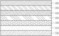
- FIG. 1 schematically illustrates a cross-section of a display device according to an exemplary embodiment of the invention.
- FIG. 2 shows a spectrum change according to ultraviolet absorption of a discoloration layer according to the exemplary embodiment of the invention.
- FIG. 3 shows a sensor of a display device in the prior art that does not include a discoloration layer.
- FIG. 4 shows a cross-section of a display device in the prior art where a near-infrared cutting layer is disposed between a display panel and a sensor.
- FIG. 5 represents a correlation of the invention between a cut wavelength and sensing performance of the optical type of fingerprint recognition sensor by using a cutting filter that cuts various wavelengths.
- FIG. 6 represents a correlation between a cut wavelength and sensing performance of the optical type of fingerprint recognition sensor by using a cutting filter that cuts various wavelengths.
- FIG. 7 represents a comparative correlation of a between a cut wavelength and sensing performance of the optical type of fingerprint recognition sensor by using a cutting filter that cuts various wavelengths.
- FIG. 8 represents a comparative correlation of a between a cut wavelength and sensing performance of the optical type of fingerprint recognition sensor by using a cutting filter that cuts various wavelengths.
- FIG. 9 illustrates a cross-section of a display device according to another exemplary embodiment of the invention.
- FIG. 10 illustrates a cross-section of a display device according to another exemplary embodiment of the invention.
- FIG. 11 illustrates a cross-section of a display device according to another exemplary embodiment of the invention.
- FIG. 12 illustrates a cross-section of a display device according to another exemplary embodiment of the invention.
- FIG. 13 illustrates a cross-section of a display device according to another exemplary embodiment of the invention.
- FIG. 14 illustrates a cross-section of a display device according to another exemplary embodiment of the invention.
- relative terms such as “lower” or “bottom” and “upper” or “top,” may be used herein to describe one element's relationship to another element as illustrated in the Figures. It will be understood that relative terms are intended to encompass different orientations of the device in addition to the orientation depicted in the Figures. For example, if the device in one of the figures is turned over, elements described as being on the “lower” side of other elements would then be oriented on “upper” sides of the other elements. The exemplary term “lower,” can therefore, encompasses both an orientation of “lower” and “upper,” depending on the particular orientation of the figure.
- the phrase “on a plane” means viewing a target portion from the top
- the phrase “on a cross-section” means viewing a cross-section formed by vertically cutting a target portion from the side.
- FIG. 1 schematically illustrates a cross-section of a display device according to an exemplary embodiment of the invention.
- a display device according to the exemplary embodiment includes a sensor 700 disposed below a display panel 100 , and a discoloration layer 400 disposed above the display panel 100 .
- the display device may include the sensor 700 that senses a fingerprint and the like, a first adhesive layer 510 that bonds the sensor 700 and the display panel 100 , a polarization layer 200 disposed on the display panel 100 , a second adhesive layer 520 that bonds the polarization layer 200 and a window 300 , and the discoloration layer 400 disposed on the window 300 .
- the first adhesive layer 510 and the second adhesive layer 520 are optional, and therefore, may be omitted depending on exemplary embodiments.
- the discoloration layer 400 is illustrated to be disposed above the window 300 , but may be positioned between the described other layers of FIG. 1 , and will depend on other exemplary embodiments.
- the discoloration layer 400 is a layer of which transmittance with respect to a wavelength of a near-infrared region (600 nm to 630 nm) will vary depending upon in indoor and outdoor environment, and sensitivity of the sensor 700 can be increased as the transmittance with respect to a specific wavelength varies according to its location in an indoor or outdoor environment. An exemplary detailed effect will be described later.
- transmittance of the discoloration layer with respect to a wavelength range of 600 nm to 630 nm will significantly change or vary depending on an indoor/outdoor environment.
- the discoloration layer 400 may have transmittance of 80% or greater with respect to a wavelength range of 600 nm to 630 nm. However, in an outdoor environment, the discoloration layer 400 may have transmittance of 10% or less with respect to a wavelength range of 600 nm to 630 nm. Accordingly, the transmittance of the discoloration layer 400 according to a wavelength of 600 nm to 630 nm may differ by 5 times to 10 times depending upon whether the display device of which the discoloration layer is part is located in an indoor and outdoor environment.
- the terms “indoor environment” and “outdoor environment” are distinguished from one another with reference to the relative amounts of ultraviolet (UV) light that the discoloration layer, which may be component part of a display device, is exposed to.
- UV ultraviolet
- both ultraviolet (UV) light and near-infrared light are regions of the electromagnetic spectrum present in natural light.
- the actual amounts of ultraviolet and near-infrared light in natural light will depend upon seasonal as well as then-current weather conditions.
- the term “outdoor environment” refers to an environment with light of greater than or equal to 1000 Lux.
- the term “indoor environment” refers to an environment with light of less 1000 Lux. A person of ordinary skill would measure the amount of light present including an amount of UV light with a light meter.
- the discoloration layer 400 may include a material of which a molecular structure is changed, e.g., such a molecular change may involve a ring-opening or ring forming isomerization, by absorption of ultraviolet (UV) light. Accordingly, as the molecular structure of the material is changed, the wavelength of light absorbed by the discoloration layer 400 also changes, and hence, there is a change in transmittance according to a wavelength of 600 nm to 630 nm.
- UV ultraviolet
- the discoloration layer 400 may include a fulgide-based material, a diarylethene-based material, or a combination of the two materials.
- the fulgide-based material implies a material that includes at least one fulgide.
- diarylethene-based material implies a material that includes at least one diarylethene.
- a molecular structure of the fulgide-based material may change due to UV absorption as shown in the following isomerization scheme below.
- the molecular scheme below is just one exemplary embodiment, and is not intended to limit the invention in any manner.
- a molecular structure of the diarylethene-based material may be reversibly changed due to UV absorption.
- the molecular scheme below is just one exemplary embodiment, and is not intended to limit the invention in any manner.
- X and Y may independently be H, a C1 to C2 alkyl group, a phenyl, or a heteroaryl.
- UV ultraviolet
- FIG. 2 represents a spectrum change according to UV absorption of the discoloration layer according to the exemplary embodiment of the invention.
- an absorption spectrum of the discoloration layer 400 according to the exemplary embodiment is shifted to the right side (to lower energy) (A to B) in the presence of UV light.
- a to B right side
- the discoloration layer 400 absorbs wavelengths at about 600 nm.
- the absorption spectrum of the discoloration layer 400 is shifted to the left side (to higher energy) (B to A).
- the discoloration layer 400 absorbs wavelengths at about 400 nm in the near-absence of UV light.
- the near-infrared light can be selectively reduced, blocked, or cut by the discoloration layer in an indoor or outdoor environment, thereby increasing sensitivity of the sensor 700 .
- FIG. 3 illustrates a sensor of a display device in the art that does not include the discoloration layer 400 .
- a display device of FIG. 3 includes a display panel 100 and a sensor 700 .
- the sensor 700 may be an optical type of fingerprint recognition sensor. Light generated from a light emission element is reflected by a finger that touches a front surface of the display panel 100 and then returns to a rear surface of the display panel 100 , and the optical fingerprint sensor of the optical type senses the light returned to the rear surface of the display panel 100 . Due to the curvature of the fingerprint, a difference in the reflection amount is generated, and the difference in the reflection amount must be recognized in the same form without a change in the surrounding environment, so that consistency of the optical fingerprint recognition can be enhanced.
- FIG. 4 shows a cross-section of a display device of the art where a near-infrared cutting layer 600 is disposed between a display panel 100 and a sensor 700 .
- a near-infrared cutting layer 600 cuts a wavelength in a near-infrared region, transmitted through the human hand, and thus the matching of optical fingerprint recognition can be improved.
- the near-infrared cutting layer 600 in FIG. 4 cuts the light reflected by the finger and returned to the rear surface, the efficiency of fingerprint recognition may be reduced. In particular, in an indoor environment where there is insufficient light, the light reflected by the finger is cut by the near-infrared cutting layer 600 and the performance of fingerprint recognition may be reduced.
- the near-infrared cutting layer 600 may also absorb light near the far red of the visible spectrum, and thus the near infrared cutting layer 600 may not be completely transparent, and exhibit a touch of color. Accordingly, the near-infrared cutting layer 600 would need to be positioned below the display panel 100 . Moreover, it may be difficult to position the near-infrared light cutting layer 600 above the display panel 100 .
- the display device includes a discoloration layer 400 disposed in a top surface of the display panel 100 .
- the discoloration layer 400 can maintain the fingerprint recognition performance of the sensor in both indoor and outdoor environments. That is, ultraviolet (UV) and near-infrared light is present in relatively large amounts in an outdoor environment compared to an indoor environment.
- a structure of the discoloration layer 400 is changed due to the presence of ultraviolet light, and thus the discoloration layer 400 absorbs light having a wavelength of 600 nm to 630 nm. That is, the near-infrared light is cut by the discoloration layer 400 , and thus performance of the optical type fingerprint recognition sensor can be maintained.
- UV and near-infrared light are present in relatively very small or trace amounts if at all compared to an outdoor environment.
- the molecular structure of the discoloration layer 400 had changed due to the absorption of ultraviolet light will return to its original structure.
- the discoloration layer 400 is transparent and does not affect display quality of the display panel 100 .
- the near-infrared light is not cut by the discoloration layer 400 , performance of the optical type fingerprint recognition sensor can be maintained.
- the display device includes the discoloration layer 400 of which an absorption spectrum will vary according to presence of ultraviolet light, and thus performance and transparency of the optical type of fingerprint recognition sensor can be maintained in both indoor and outdoor environments. That is, in an outdoor environment where ultraviolet and near-infrared light is present, the molecular structure of the discoloration layer 400 changes to a molecular structure that absorbs near-infrared light, and performance of the fingerprint recognition sensor can be maintained. Moreover, in the indoor environment where there is a small amount of ultraviolet and near-infrared light, the molecular structure of the discoloration layer 400 changes to a molecular structure that transmits visible light such that transparency can be maintained, and performance of the fingerprint recognition sensor can be maintained.
- FIG. 5 to FIG. 8 are provided to determine a correlation between a cut wavelength and sensing performance of the optical type of fingerprint recognition sensor by using a cutting filter that cuts various wavelengths.
- a sensor 700 is located inside a case 900 , and filters 1100 , 1200 , and 1300 , respectively, block different wavelengths positioned at an entrance of the case 900 .
- blocking light means that a component of the display device, e.g., a filter layer or a discoloration layer, will reduce the transmittance of light of a stated wavelength, wavelength range, or a region of the electromagnetic spectrum, by at least 80%, preferably, by at least 90%.
- the experiment results shown in FIG. 5 to FIG. 8 show that blocking light of about a 600 nm wavelength can improve performance of the optical type of fingerprint recognition sensor.
- the discoloration layer 400 of the display device according to the exemplary embodiment can improve performance of the optical type of fingerprint recognition sensor because transmittance with respect to light having a wavelength of about 600 nm to about 630 nm in an outdoor environment where ultraviolet and near-infrared light is present is less than 10%.
- the discoloration layer 400 is disposed above the window 300 , but this need not be the case as other embodiments can have the discoloration layer positioned between the window and the sensor.
- FIG. 9 illustrates a cross-section that is similar to the cross-section shown in FIG. 1 with respect to a display device according to another exemplary embodiment.
- a display device according to the exemplary embodiment further includes a hard coating layer 800 disposed above a discoloration layer 400 .
- the display device according to the exemplary embodiment of FIG. 9 is similar to the display device of FIG. 1 except for the configuration of the hard coating layer 800 , and therefore detailed descriptions of identical constituent elements are omitted.
- FIG. 10 illustrates a cross-section that is similar to the cross-section shown in FIG. 1 in a display device according to another exemplary embodiment except that a discoloration layer 400 is disposed between a window 300 and a second adhesive layer 520 . Detailed descriptions of identical constituent elements are omitted.
- a discoloration layer 400 is disposed between the window 300 and the second adhesive layer 520
- the absorption spectrum of the discoloration layer 400 changes as the device location changes from an indoor to an outdoor environment such that near-infrared light can be selectively blocked.
- FIG. 11 illustrates a cross-section that is similar to the cross-section shown in FIG. 1 in a display device according to another exemplary embodiment except that a discoloration adhesive layer 410 is a combination of an adhesive layer and a discoloration layer material, instead of a separate discoloration layer 400 and a second adhesive layer 520 .
- a discoloration adhesive layer 410 is a combination of an adhesive layer and a discoloration layer material, instead of a separate discoloration layer 400 and a second adhesive layer 520 .
- a discoloration adhesive layer 410 is a combination of an adhesive layer and a discoloration layer material, instead of a separate discoloration layer 400 and a second adhesive layer 520 .
- Detailed descriptions of identical constituent elements are omitted.
- the second adhesive layer 520 and the discoloration layer 400 are integrated with the discoloration adhesive layer 410 .
- the discoloration adhesive layer 410 includes an adhesive material and a discoloration material included in the adhesive material, and is able to bond with a window 300 and a polarization layer 200 , and selectively blocks near-infrared light since an absorption spectrum of the discoloration adhesive layer 410 changes as the device location changes from an indoor to an outdoor environment.
- FIG. 12 illustrates a cross-section that is similar to the cross-section shown in FIG. 1 in a display device according to another exemplary embodiment except that a discoloration layer 400 is disposed between a first adhesive layer 510 and a sensor 700 .
- the discoloration layer 400 is disposed above the display panel 100 , but the same effect can be obtained when the discoloration layer 400 is disposed below the display panel 100 . It may be preferable for the discoloration layer 400 to be disposed below the display panel 100 in an outdoor environment, and even if the discoloration layer 400 loses some transparency, it does not affect the display quality.
- FIG. 13 illustrates a cross-section that is similar to the cross-section shown in FIG. 12 in a display device according to another exemplary embodiment.
- the display device according to the exemplary embodiment of FIG. 12 is the same as the display device of FIG. 1 , except that a discoloration layer 400 is disposed between a first adhesive layer 510 and a display panel 100 .
- the effect is the same as in the exemplary embodiment of FIG. 12 , and thus a detailed description is omitted.
- FIG. 14 illustrates a cross-section that is the same as the cross-section shown in FIG. 12 in a display device according to another exemplary embodiment except that a discoloration adhesive layer 410 , which is a combination of an adhesive layer and a discoloration material, is included instead of a separate discoloration layer 400 and a first adhesive layer 510 . Detailed descriptions of identical constituent elements is omitted.
- the first adhesive layer 510 and the discoloration layer 400 are integrated with the discoloration adhesive layer 410 .
- the discoloration adhesive layer 410 includes an adhesive material and a discoloration material included in the adhesive material, and bonds with a display panel 100 and a sensor 700 , and selectively blocks near-infrared light because an absorption spectrum of the discoloration adhesive layer 410 changes as the device location changes from an indoor to an outdoor environment.
Landscapes
- Physics & Mathematics (AREA)
- Nonlinear Science (AREA)
- General Physics & Mathematics (AREA)
- Engineering & Computer Science (AREA)
- Optics & Photonics (AREA)
- Multimedia (AREA)
- Theoretical Computer Science (AREA)
- Human Computer Interaction (AREA)
- Mathematical Physics (AREA)
- Chemical & Material Sciences (AREA)
- Crystallography & Structural Chemistry (AREA)
- Devices For Indicating Variable Information By Combining Individual Elements (AREA)
- Liquid Crystal (AREA)
- Optical Filters (AREA)
Abstract
Description


Claims (18)
Applications Claiming Priority (2)
| Application Number | Priority Date | Filing Date | Title |
|---|---|---|---|
| KR10-2019-0174432 | 2019-12-24 | ||
| KR1020190174432A KR20210082320A (en) | 2019-12-24 | 2019-12-24 | Display decvice |
Publications (2)
| Publication Number | Publication Date |
|---|---|
| US20210191161A1 US20210191161A1 (en) | 2021-06-24 |
| US12050370B2 true US12050370B2 (en) | 2024-07-30 |
Family
ID=76438133
Family Applications (1)
| Application Number | Title | Priority Date | Filing Date |
|---|---|---|---|
| US17/114,742 Active US12050370B2 (en) | 2019-12-24 | 2020-12-08 | Display device |
Country Status (2)
| Country | Link |
|---|---|
| US (1) | US12050370B2 (en) |
| KR (1) | KR20210082320A (en) |
Families Citing this family (1)
| Publication number | Priority date | Publication date | Assignee | Title |
|---|---|---|---|---|
| KR102894136B1 (en) * | 2020-03-06 | 2025-12-04 | 삼성디스플레이 주식회사 | Display device and method of manufacturing the same |
Citations (13)
| Publication number | Priority date | Publication date | Assignee | Title |
|---|---|---|---|---|
| US20070041073A1 (en) * | 2004-05-17 | 2007-02-22 | Anil Kumar | Polarizing, photochromic devices and methods of making the same |
| US20070053047A1 (en) * | 2003-07-01 | 2007-03-08 | Anil Kumar | Polarizing, photochromic devices and methods of making the same |
| US8205551B2 (en) | 2005-12-08 | 2012-06-26 | Essilor International (Compagnie Generale D'optique) | Method for transferring a micron-sized pattern onto an optical article and optical article thus obtained |
| US20150109651A1 (en) * | 2012-05-29 | 2015-04-23 | Switch Materials Inc. | Optical filter comprising a variable transmittance layer |
| KR20150127209A (en) | 2013-03-20 | 2015-11-16 | 에실러에떼르나쇼날(꽁빠니제네랄돕띠끄) | Polyurethane based adhesive for polarizing structure and polarized lens |
| US20170178595A1 (en) * | 2015-12-17 | 2017-06-22 | Samsung Display Co., Ltd. | Transparent display panel and transparent display device including the same |
| JP2017193115A (en) * | 2016-04-21 | 2017-10-26 | パイロットインキ株式会社 | Photochromic laminate |
| US20180121703A1 (en) * | 2016-10-28 | 2018-05-03 | Samsung Electronics Co., Ltd. | Apparatus for reducing noise input to fingerprint sensor |
| KR20180053035A (en) | 2016-11-11 | 2018-05-21 | 엘지디스플레이 주식회사 | Organic light emitting display device |
| KR20180059720A (en) | 2016-11-25 | 2018-06-05 | 엘지디스플레이 주식회사 | Display device |
| US20190012510A1 (en) * | 2017-07-04 | 2019-01-10 | Boe Technology Group Co., Ltd. | Optical fingerprint identification device, fingerprint identification method thereof and display device |
| CN109284655A (en) | 2017-07-20 | 2019-01-29 | 南昌欧菲生物识别技术有限公司 | Handheld terminal and its fingerprint recognition mould group |
| US20190073505A1 (en) * | 2017-09-05 | 2019-03-07 | Lg Display Co., Ltd. | Display device including a fingerprint scanner |
-
2019
- 2019-12-24 KR KR1020190174432A patent/KR20210082320A/en active Pending
-
2020
- 2020-12-08 US US17/114,742 patent/US12050370B2/en active Active
Patent Citations (15)
| Publication number | Priority date | Publication date | Assignee | Title |
|---|---|---|---|---|
| US20070053047A1 (en) * | 2003-07-01 | 2007-03-08 | Anil Kumar | Polarizing, photochromic devices and methods of making the same |
| US20070041073A1 (en) * | 2004-05-17 | 2007-02-22 | Anil Kumar | Polarizing, photochromic devices and methods of making the same |
| US8205551B2 (en) | 2005-12-08 | 2012-06-26 | Essilor International (Compagnie Generale D'optique) | Method for transferring a micron-sized pattern onto an optical article and optical article thus obtained |
| KR101421238B1 (en) | 2005-12-08 | 2014-07-30 | 에씰로아 인터내셔날(콩파니에 제네랄 도프티크) | A method of transferring a micron-sized pattern onto an optical article, and an optical article |
| JP6463673B2 (en) | 2012-05-29 | 2019-02-06 | スイッチ マテリアルズ インコーポレイテッドSwitch Materials Inc. | Optical filter including a variable transmittance layer |
| US20150109651A1 (en) * | 2012-05-29 | 2015-04-23 | Switch Materials Inc. | Optical filter comprising a variable transmittance layer |
| KR20150127209A (en) | 2013-03-20 | 2015-11-16 | 에실러에떼르나쇼날(꽁빠니제네랄돕띠끄) | Polyurethane based adhesive for polarizing structure and polarized lens |
| US20170178595A1 (en) * | 2015-12-17 | 2017-06-22 | Samsung Display Co., Ltd. | Transparent display panel and transparent display device including the same |
| JP2017193115A (en) * | 2016-04-21 | 2017-10-26 | パイロットインキ株式会社 | Photochromic laminate |
| US20180121703A1 (en) * | 2016-10-28 | 2018-05-03 | Samsung Electronics Co., Ltd. | Apparatus for reducing noise input to fingerprint sensor |
| KR20180053035A (en) | 2016-11-11 | 2018-05-21 | 엘지디스플레이 주식회사 | Organic light emitting display device |
| KR20180059720A (en) | 2016-11-25 | 2018-06-05 | 엘지디스플레이 주식회사 | Display device |
| US20190012510A1 (en) * | 2017-07-04 | 2019-01-10 | Boe Technology Group Co., Ltd. | Optical fingerprint identification device, fingerprint identification method thereof and display device |
| CN109284655A (en) | 2017-07-20 | 2019-01-29 | 南昌欧菲生物识别技术有限公司 | Handheld terminal and its fingerprint recognition mould group |
| US20190073505A1 (en) * | 2017-09-05 | 2019-03-07 | Lg Display Co., Ltd. | Display device including a fingerprint scanner |
Also Published As
| Publication number | Publication date |
|---|---|
| US20210191161A1 (en) | 2021-06-24 |
| KR20210082320A (en) | 2021-07-05 |
Similar Documents
| Publication | Publication Date | Title |
|---|---|---|
| KR102537758B1 (en) | Display device with a built-in optical image sensor | |
| JP2023099595A (en) | Electronic apparatus | |
| US10216020B2 (en) | Display device with cover window | |
| CN204241803U (en) | Mirror display | |
| KR101720588B1 (en) | Foldable organic light emitting diode display | |
| WO2017210925A1 (en) | Metal wire grating polarizing sheet and liquid crystal display apparatus | |
| CN211554956U (en) | Fingerprint sensing module and electronic device | |
| KR20190010777A (en) | Display apparatus and manufacturimg method thereof | |
| US20180335667A1 (en) | Backlight module and display device containing the same | |
| US10438042B2 (en) | Optical fingerprint recognition sensor | |
| US12050370B2 (en) | Display device | |
| CN105278154A (en) | Liquid crystal display device and liquid crystal display panel thereof | |
| US20120188173A1 (en) | Touch panel assembly | |
| US20110012839A1 (en) | Stacking assembly of a touch panel | |
| CN112904465B (en) | Light control member, display device, and method for manufacturing display device | |
| US20220139103A1 (en) | Electronic device and optical fingerprint recognition module thereof | |
| US8611012B2 (en) | Light guide plate | |
| TWI634470B (en) | Polarized capacitive touch panel and display of the same | |
| TW202219829A (en) | Image capture device | |
| KR102542872B1 (en) | Fingerprint sensing module and display device with a built-in optical image sensor | |
| KR20240014113A (en) | Display device and position input system including the same | |
| KR20190019308A (en) | Display Device Having A Fingerprint Sensor | |
| CN120265458A (en) | Composite sheet with retardation plate | |
| US11714310B2 (en) | Display device | |
| CN117706837A (en) | Display module and display device |
Legal Events
| Date | Code | Title | Description |
|---|---|---|---|
| AS | Assignment |
Owner name: SAMSUNG DISPLAY CO., LTD., KOREA, REPUBLIC OF Free format text: ASSIGNMENT OF ASSIGNORS INTEREST;ASSIGNORS:LEE, SANG-GU;YOU, JUN WOO;KIM, ONNURI;AND OTHERS;REEL/FRAME:054644/0316 Effective date: 20200601 |
|
| FEPP | Fee payment procedure |
Free format text: ENTITY STATUS SET TO UNDISCOUNTED (ORIGINAL EVENT CODE: BIG.); ENTITY STATUS OF PATENT OWNER: LARGE ENTITY |
|
| STPP | Information on status: patent application and granting procedure in general |
Free format text: APPLICATION DISPATCHED FROM PREEXAM, NOT YET DOCKETED |
|
| STPP | Information on status: patent application and granting procedure in general |
Free format text: DOCKETED NEW CASE - READY FOR EXAMINATION |
|
| STPP | Information on status: patent application and granting procedure in general |
Free format text: NON FINAL ACTION MAILED |
|
| STPP | Information on status: patent application and granting procedure in general |
Free format text: RESPONSE TO NON-FINAL OFFICE ACTION ENTERED AND FORWARDED TO EXAMINER |
|
| STPP | Information on status: patent application and granting procedure in general |
Free format text: FINAL REJECTION MAILED |
|
| STPP | Information on status: patent application and granting procedure in general |
Free format text: RESPONSE AFTER FINAL ACTION FORWARDED TO EXAMINER |
|
| STPP | Information on status: patent application and granting procedure in general |
Free format text: ADVISORY ACTION MAILED |
|
| STPP | Information on status: patent application and granting procedure in general |
Free format text: DOCKETED NEW CASE - READY FOR EXAMINATION |
|
| STPP | Information on status: patent application and granting procedure in general |
Free format text: NON FINAL ACTION MAILED |
|
| STPP | Information on status: patent application and granting procedure in general |
Free format text: RESPONSE AFTER FINAL ACTION FORWARDED TO EXAMINER |
|
| STPP | Information on status: patent application and granting procedure in general |
Free format text: ADVISORY ACTION MAILED |
|
| STPP | Information on status: patent application and granting procedure in general |
Free format text: RESPONSE AFTER FINAL ACTION FORWARDED TO EXAMINER |
|
| STPP | Information on status: patent application and granting procedure in general |
Free format text: DOCKETED NEW CASE - READY FOR EXAMINATION |
|
| STPP | Information on status: patent application and granting procedure in general |
Free format text: NON FINAL ACTION MAILED |
|
| STPP | Information on status: patent application and granting procedure in general |
Free format text: RESPONSE TO NON-FINAL OFFICE ACTION ENTERED AND FORWARDED TO EXAMINER |
|
| STPP | Information on status: patent application and granting procedure in general |
Free format text: NOTICE OF ALLOWANCE MAILED -- APPLICATION RECEIVED IN OFFICE OF PUBLICATIONS |
|
| ZAAA | Notice of allowance and fees due |
Free format text: ORIGINAL CODE: NOA |
|
| ZAAB | Notice of allowance mailed |
Free format text: ORIGINAL CODE: MN/=. |
|
| STPP | Information on status: patent application and granting procedure in general |
Free format text: PUBLICATIONS -- ISSUE FEE PAYMENT RECEIVED |
|
| STPP | Information on status: patent application and granting procedure in general |
Free format text: PUBLICATIONS -- ISSUE FEE PAYMENT VERIFIED |
|
| STCF | Information on status: patent grant |
Free format text: PATENTED CASE |