US12048218B2 - Electroluminescent display device comprising trenches between adjacent subpixels - Google Patents
Electroluminescent display device comprising trenches between adjacent subpixels Download PDFInfo
- Publication number
- US12048218B2 US12048218B2 US17/551,837 US202117551837A US12048218B2 US 12048218 B2 US12048218 B2 US 12048218B2 US 202117551837 A US202117551837 A US 202117551837A US 12048218 B2 US12048218 B2 US 12048218B2
- Authority
- US
- United States
- Prior art keywords
- trench
- subpixel
- layer
- hole
- light emitting
- Prior art date
- Legal status (The legal status is an assumption and is not a legal conclusion. Google has not performed a legal analysis and makes no representation as to the accuracy of the status listed.)
- Active, expires
Links
Images


Classifications
-
- H—ELECTRICITY
- H10—SEMICONDUCTOR DEVICES; ELECTRIC SOLID-STATE DEVICES NOT OTHERWISE PROVIDED FOR
- H10K—ORGANIC ELECTRIC SOLID-STATE DEVICES
- H10K59/00—Integrated devices, or assemblies of multiple devices, comprising at least one organic light-emitting element covered by group H10K50/00
- H10K59/10—OLED displays
- H10K59/12—Active-matrix OLED [AMOLED] displays
- H10K59/122—Pixel-defining structures or layers, e.g. banks
-
- H—ELECTRICITY
- H10—SEMICONDUCTOR DEVICES; ELECTRIC SOLID-STATE DEVICES NOT OTHERWISE PROVIDED FOR
- H10K—ORGANIC ELECTRIC SOLID-STATE DEVICES
- H10K59/00—Integrated devices, or assemblies of multiple devices, comprising at least one organic light-emitting element covered by group H10K50/00
- H10K59/10—OLED displays
- H10K59/12—Active-matrix OLED [AMOLED] displays
- H10K59/124—Insulating layers formed between TFT elements and OLED elements
-
- G—PHYSICS
- G02—OPTICS
- G02B—OPTICAL ELEMENTS, SYSTEMS OR APPARATUS
- G02B27/00—Optical systems or apparatus not provided for by any of the groups G02B1/00 - G02B26/00, G02B30/00
- G02B27/01—Head-up displays
-
- H—ELECTRICITY
- H10—SEMICONDUCTOR DEVICES; ELECTRIC SOLID-STATE DEVICES NOT OTHERWISE PROVIDED FOR
- H10K—ORGANIC ELECTRIC SOLID-STATE DEVICES
- H10K50/00—Organic light-emitting devices
- H10K50/10—OLEDs or polymer light-emitting diodes [PLED]
- H10K50/14—Carrier transporting layers
- H10K50/15—Hole transporting layers
- H10K50/156—Hole transporting layers comprising a multilayered structure
-
- H—ELECTRICITY
- H10—SEMICONDUCTOR DEVICES; ELECTRIC SOLID-STATE DEVICES NOT OTHERWISE PROVIDED FOR
- H10K—ORGANIC ELECTRIC SOLID-STATE DEVICES
- H10K50/00—Organic light-emitting devices
- H10K50/10—OLEDs or polymer light-emitting diodes [PLED]
- H10K50/17—Carrier injection layers
-
- H—ELECTRICITY
- H10—SEMICONDUCTOR DEVICES; ELECTRIC SOLID-STATE DEVICES NOT OTHERWISE PROVIDED FOR
- H10K—ORGANIC ELECTRIC SOLID-STATE DEVICES
- H10K50/00—Organic light-emitting devices
- H10K50/10—OLEDs or polymer light-emitting diodes [PLED]
- H10K50/19—Tandem OLEDs
-
- H—ELECTRICITY
- H10—SEMICONDUCTOR DEVICES; ELECTRIC SOLID-STATE DEVICES NOT OTHERWISE PROVIDED FOR
- H10K—ORGANIC ELECTRIC SOLID-STATE DEVICES
- H10K50/00—Organic light-emitting devices
- H10K50/80—Constructional details
- H10K50/85—Arrangements for extracting light from the devices
- H10K50/856—Arrangements for extracting light from the devices comprising reflective means
-
- H—ELECTRICITY
- H10—SEMICONDUCTOR DEVICES; ELECTRIC SOLID-STATE DEVICES NOT OTHERWISE PROVIDED FOR
- H10K—ORGANIC ELECTRIC SOLID-STATE DEVICES
- H10K50/00—Organic light-emitting devices
- H10K50/80—Constructional details
- H10K50/85—Arrangements for extracting light from the devices
- H10K50/858—Arrangements for extracting light from the devices comprising refractive means, e.g. lenses
-
- H—ELECTRICITY
- H10—SEMICONDUCTOR DEVICES; ELECTRIC SOLID-STATE DEVICES NOT OTHERWISE PROVIDED FOR
- H10K—ORGANIC ELECTRIC SOLID-STATE DEVICES
- H10K59/00—Integrated devices, or assemblies of multiple devices, comprising at least one organic light-emitting element covered by group H10K50/00
- H10K59/10—OLED displays
- H10K59/12—Active-matrix OLED [AMOLED] displays
- H10K59/121—Active-matrix OLED [AMOLED] displays characterised by the geometry or disposition of pixel elements
-
- H—ELECTRICITY
- H10—SEMICONDUCTOR DEVICES; ELECTRIC SOLID-STATE DEVICES NOT OTHERWISE PROVIDED FOR
- H10K—ORGANIC ELECTRIC SOLID-STATE DEVICES
- H10K59/00—Integrated devices, or assemblies of multiple devices, comprising at least one organic light-emitting element covered by group H10K50/00
- H10K59/30—Devices specially adapted for multicolour light emission
- H10K59/35—Devices specially adapted for multicolour light emission comprising red-green-blue [RGB] subpixels
- H10K59/353—Devices specially adapted for multicolour light emission comprising red-green-blue [RGB] subpixels characterised by the geometrical arrangement of the RGB subpixels
-
- H—ELECTRICITY
- H10—SEMICONDUCTOR DEVICES; ELECTRIC SOLID-STATE DEVICES NOT OTHERWISE PROVIDED FOR
- H10K—ORGANIC ELECTRIC SOLID-STATE DEVICES
- H10K59/00—Integrated devices, or assemblies of multiple devices, comprising at least one organic light-emitting element covered by group H10K50/00
- H10K59/80—Constructional details
- H10K59/875—Arrangements for extracting light from the devices
- H10K59/876—Arrangements for extracting light from the devices comprising a resonant cavity structure, e.g. Bragg reflector pair
-
- H—ELECTRICITY
- H10—SEMICONDUCTOR DEVICES; ELECTRIC SOLID-STATE DEVICES NOT OTHERWISE PROVIDED FOR
- H10K—ORGANIC ELECTRIC SOLID-STATE DEVICES
- H10K59/00—Integrated devices, or assemblies of multiple devices, comprising at least one organic light-emitting element covered by group H10K50/00
- H10K59/80—Constructional details
- H10K59/875—Arrangements for extracting light from the devices
- H10K59/878—Arrangements for extracting light from the devices comprising reflective means
Definitions
- the present disclosure relates to an electroluminescent display device.
- An electroluminescent display device has a structure in which a light emitting layer is formed between an anode electrode and a cathode electrode, and is a device for displaying an image by allowing the light emitting layer to emit light through an electric field between the two electrodes.
- the light emitting layer may be made of an organic material for emitting light by transiting exciton generated by combination of electrons and holes from an excited state to a ground state, or may be made of an inorganic material such as quantum dot.
- the light emitting layer may be provided to emit light of respective colors different per subpixel, for example, red light, green light and blue light per subpixel, or may be provided to emit light of the same color per subpixel, for example, white light.
- subpixels In order to obtain an electroluminescent display device of high resolution, subpixels should be formed at a compact interval, and in this case, a leakage current occurs in a boundary area between adjacent subpixels, whereby a problem occurs in that image quality is deteriorated.
- the present disclosure has been made in view of the above problems and is to provide an electroluminescent display device that can prevent a leakage current from occurring in a boundary area between adjacent subpixels and reducing deterioration of image quality due to the leakage current.
- an electroluminescent display device comprising a substrate having a first subpixel and a second subpixel, which are adjacent to each other, a first electrode provided in each of the first subpixel and the second subpixel on the substrate, a trench including a first trench and a second trench, which are provided to be spaced apart from each other at a boundary between the first subpixel and the second subpixel on the substrate, a light emitting layer provided on the first electrode and provided in the first subpixel, the second subpixel and a boundary between the first subpixel and the second subpixel, and a second electrode provided on the light emitting layer, wherein a first portion of the light emitting layer is discontinuous in the first trench and the second trench, a second portion of the light emitting layer is discontinuous in the first trench and is continuous in an area overlapped with the second trench, and a third portion of the light emitting layer is continuous in an area overlapped with the first trench and the second trench.
- an electroluminescent display device comprising a substrate having a first subpixel, a second subpixel and a third subpixel, which are arranged in a first direction, a first electrode provided in each of the first subpixel, the second subpixel and the third subpixel on the substrate, a trench including a first trench and a second trench, which are respectively provided in a boundary area between the first subpixel and the second subpixel and a boundary area between the second subpixel and the third subpixel, a light emitting layer provided on the first electrode and provided in the trench, and a second electrode provided on the light emitting layer, wherein a portion of the light emitting layer is discontinuous in the first trench and the second trench, and a portion of the light emitting layer, which is discontinuous in the first trench, is thicker than a portion of the light emitting layer, which is discontinuous in the second trench.
- FIG. 1 is a schematic plan view illustrating an electroluminescent display device according to one aspect of the present disclosure
- FIG. 2 is a schematic cross-sectional view illustrating an electroluminescent display device according to one aspect of the present disclosure, taken along line I-I′ of FIG. 1 ;
- FIG. 3 is a cross-sectional view illustrating a deposited structure of a light emitting layer according to one aspect of the present disclosure
- FIG. 4 is a detailed cross-sectional view illustrating a trench area in an electroluminescent display device according to one aspect of the present disclosure
- FIG. 5 is a detailed cross-sectional view illustrating a trench area in an electroluminescent display device according to another aspect of the present disclosure
- FIGS. 6 A to 6 E are schematic cross-sectional views illustrating a manufacturing process of an electroluminescent display device according to one aspect of the present disclosure
- FIG. 7 is a schematic plan view illustrating an electroluminescent display device according to another aspect of the present disclosure.
- FIG. 8 is a schematic plan view illustrating an electroluminescent display device according to still another aspect of the present disclosure.
- FIGS. 9 A to 9 C are views illustrating an electroluminescent display device according to still further another aspect of the present disclosure.
- FIG. 1 is a schematic plan view illustrating an electroluminescent display device according to one aspect of the present disclosure.
- the electroluminescent display device includes a substrate 100 , first electrodes 510 , 520 and 530 , and trenches T 1 and T 2 .
- a plurality of subpixels SP 1 , SP 2 and SP 3 are formed on the substrate 100 .
- the plurality of subpixels SP 1 , SP 2 and SP 3 may include, but are not limited to, a first subpixel SP 1 , a second subpixel SP 2 and a third subpixel SP 3 , which are arranged in a first direction, for example, in a horizontal direction.
- the first subpixel SP 1 may be provided to emit light of a first color, for example, red light
- the second subpixel SP 2 may be provided to emit light of a second color, for example, green light
- the third subpixel SP 3 may be provided to emit light of a third color, for example, blue light, but these subpixels are not limited thereto.
- the arrangement structure of the plurality of subpixels SP 1 , SP 2 and SP 3 may be changed to various structures known in the art.
- the first electrodes 510 , 520 and 530 are formed to be patterned in the first to third subpixels SP 1 , SP 2 and SP 3 , respectively. That is, one first electrode 510 is formed in the first subpixel SP 1 , another first electrode 520 is formed in the second subpixel SP 2 , and the other first electrode 530 is formed in the third subpixel SP 3 .
- the first electrodes 510 , 520 and 530 may serve as anodes in the first to third subpixels SP 1 , SP 2 and SP 3 , and are electrically connected to a source electrode or a drain electrode of a driving thin film transistor formed to be patterned in each of the first to third subpixels SP 1 , SP 2 and SP 3 .
- the trenches T 1 and T 2 are formed in boundary areas among the plurality of subpixels SP 1 , SP 2 and SP 3 .
- the trenches T 1 and T 2 are formed in the boundary area between the first subpixel SP 1 and the second subpixel SP 2 and the boundary area between the second subpixel SP 2 and the third subpixel SP 3 .
- the trenches T 1 and T 2 serve to prevent a leakage current between adjacent subpixels SP 1 , SP 2 and SP 3 .
- the subpixels SP 1 , SP 2 and SP 3 are provided at compact intervals to embody high resolution. In this case, when light is emitted from the light emitting layer in one of the subpixels SP 1 , SP 2 and SP 3 , charges in the corresponding light emitting layer move to the light emitting layer in another adjacent one of the subpixels SP 1 , SP 2 and SP 3 , whereby a leakage current may occur.
- a portion of the light emitting layer in one of the subpixel SP 1 , SP 2 and SP 3 and a portion of the light emitting layer in another adjacent one of the subpixels SP 1 , SP 2 and SP 3 can be disconnected from one another in the trenches T 1 and T 2 , whereby a leakage current can be prevented between the adjacent subpixels SP 1 , SP 2 and SP 3 .
- the trenches T 1 and T 2 may include a first trench T 1 and a second trench T 2 .
- the first trench T 1 is provided to have a first width w 1 , and is formed in an area between the first electrode 510 of the first subpixel SP 1 and the first electrode 520 of the second subpixel SP 2 and an area between the first electrode 520 of the second subpixel SP 2 and the first electrode 530 of the third subpixel SP 3 , respectively.
- the second trench T 2 is provided to have a second width w 2 , and may be provided on left and right sides of the first trench T 1 .
- the second trench T 2 may be formed in an area between the first electrode 510 of the first subpixel SP 1 and the first trench T 1 and an area between the first trench T 1 and the first electrode 520 of the second subpixel SP 2 .
- the second trench T 2 may be formed in an area between the first electrode 520 of the second subpixel SP 2 and the first trench T 1 and an area between the first trench T 1 and the first electrode 530 of the third subpixel SP 3 .
- the second trench T 2 may be formed only on one of the left side and the right side of the first trench T 1 .
- the first width w 1 of the first trench T 1 is wider than the second width w 2 of the second trench T 2 . Therefore, a portion of the light emitting layer disconnected in the first trench T 1 and a portion of the light emitting layer disconnected in the second trench T 2 are different from each other, and this case will be described later.
- FIG. 2 is a schematic cross-sectional view illustrating an electroluminescent display device according to one aspect of the present disclosure, taken along line I-I′ of FIG. 1 .
- the electroluminescent display device includes a substrate 100 , a circuit element layer 200 , reflective layers 310 , 320 and 330 , insulating layers 410 and 420 , first electrodes 510 , 520 and 530 , a fence structure 600 , a light emitting layer 700 , a second electrode 800 , an encapsulation layer 850 and color filter layers 910 , 920 and 930 .
- the substrate 100 may be made of glass or plastic, but is not limited thereto.
- the substrate 100 may be made of a semiconductor material such as a silicon wafer.
- a first subpixel SP 1 , a second subpixel SP 2 and a third subpixel SP 3 are provided on the substrate 100 .
- the first subpixel SP 1 may be provided to emit red (R) light
- the second subpixel SP 2 may be provided to emit green (G) light
- the third subpixel SP 3 may be provided to emit blue (B) light, but these subpixels are not limited thereto.
- the electroluminescent display device may be provided in a top emission type in which emitted light is emitted to an upper side, and thus an opaque material as well as a transparent material may be used as a material of the substrate 100 .
- the circuit element layer 200 is formed on the substrate 100 .
- the circuit element layer 200 includes a circuit element that includes various signal lines, a thin film transistor and a capacitor, wherein the circuit element is provided for each of the subpixels SP 1 , SP 2 and SP 3 .
- the signal lines may include a gate line, a data line, a power line and a reference line
- the thin film transistor may include a switching thin film transistor, a driving thin film transistor and a sensing thin film transistor.
- the switching thin film transistor is switched in accordance with a gate signal supplied to the gate line to supply a data voltage supplied from the data line to the driving thin film transistor.
- the driving thin film transistor is switched in accordance with the data voltage supplied from the switching thin film transistor to generate a data current from a power source supplied from the power line and supply the data current to the first electrodes 510 , 520 and 530 .
- the sensing thin film transistor serves to sense a threshold voltage deviation of the driving thin film transistor, which causes degradation of image quality, and supplies the current of the driving thin film transistor to the reference line in response to a sensing control signal supplied from the gate line or a separate sensing line.
- the capacitor serves to maintain a data voltage supplied to the driving thin film transistor for one frame, and is connected to each of a gate terminal and a source terminal of the driving thin film transistor.
- the circuit element layer 200 may further include a passivation layer for protecting the switching thin film transistor, the driving thin film transistor and the sensing thin film transistor, and a planarization layer provided on the passivation layer.
- the reflective layers 310 , 320 and 330 are formed to be patterned on the circuit element layer 200 for each of the subpixels SP 1 , SP 2 and SP 3 .
- the first reflective layer 310 is formed to be patterned in the first subpixel SP 1
- the second reflective layer 320 is formed to be patterned in the second subpixel SP 2
- the third reflective layer 330 is formed to be patterned in the third subpixel SP 3 .
- the reflective layers 310 , 320 and 330 are provided so that micro cavity characteristics may be embodied in each of the subpixels SP 1 , SP 2 and SP 3 . Therefore, a distance from the first reflective layer 310 to the second electrode 800 may be longer than a distance from the second reflective layer 320 to the second electrode 800 , and the distance from the second reflective layer 320 to the second electrode 800 may be longer than a distance from the third reflective layer 330 to the second electrode 800 .
- the first reflective layer 310 may be formed on an upper surface of the circuit element layer 200
- the second reflective layer 320 may be formed on an upper surface of the first insulating layer 410
- the third reflective layer 330 may be formed on an upper surface of the second insulating layer 420 .
- the first reflective layer 310 may electrically be insulated from the first electrode 510 of the first subpixel SP 1 , but may electrically be connected with the first electrode 510 of the first subpixel SP 1 through a contact hole provided in the insulating layers 410 and 420 .
- the second reflective layer 320 may electrically be insulated from the first electrode 520 of the second subpixel SP 2 , but may electrically be connected with the first electrode 520 of the second subpixel SP 2 through a contact hole provided in the second insulating layer 420 .
- the third reflective layer 330 may be provided to be in contact with a lower surface of the first electrode 530 of the third subpixel SP 3
- an insulating layer may be provided between the third reflective layer 330 and the first electrode 530 of the third subpixel SP 3 as the case may be.
- the insulating layers 410 and 420 include a first insulating layer 410 provided on the circuit element layer 200 and a second insulating layer 420 disposed on the first insulating layer 410 .
- the first insulating layer 410 includes a first hole 411 and a second hole 412 .
- the first hole 411 and the second hole 412 of the first insulating layer 410 may be provided in a boundary area between the first subpixel SP 1 and the second subpixel SP 2 and provided to pass through the first insulating layer 410 , but is not limited thereto.
- the first hole 411 of the first insulating layer 410 is provided between the first electrode 510 of the first subpixel SP 1 and the first electrode 520 of the second subpixel SP 2 and between the first electrode 520 of the second subpixel SP 2 and the first electrode 530 of the third subpixel SP 3 , respectively.
- a width w 1 of the first hole 411 of the first insulating layer 410 may be the same as the first width w 1 of the first trench T 1 .
- the second hole 412 of the first insulating layer 410 may respectively be provided on left and right sides of the first hole 411 of the first insulating layer 410 .
- the second hole 412 of the first insulating layer 410 is disposed in an area between the first electrode 510 of the first subpixel SP 1 and the first hole 411 of the first insulating layer 410 and an area between the first hole 411 of the first insulating layer 410 and the first electrode 520 of the second subpixel SP 2 .
- the second hole 412 of the first insulating layer 410 is disposed in an area between the first electrode 520 of the second subpixel SP 2 and the first hole 411 of the first insulating layer 410 and an area between the first hole 411 of the first insulating layer 410 and the first electrode 530 of the third subpixel SP 3 .
- a width W 3 of the second hole 412 of the first insulating layer 410 may be the same as the width w 1 of the first hole 411 of the first insulating layer 410 , but may be different from the width w 1 of the first hole 411 of the first insulating layer 410 as the case may be.
- the second insulating layer 420 includes a first hole 421 and a second hole 422 .
- the first hole 421 and the second hole 422 of the second insulating layer 420 are provided in a boundary area between the first subpixel SP 1 and the second subpixel SP 2 .
- the first hole 421 of the second insulating layer 420 passes through the second insulating layer 420 , and is provided to be communicated with the first hole 411 of the first insulating layer 410 while being overlapped with the first hole 411 of the first insulating layer 410 .
- the width w 1 of the first hole 421 of the second insulating layer 420 may be the same as the width w 1 of the first hole 411 of the first insulating layer 410 .
- the second hole 422 of the second insulating layer 420 is formed without passing through the second insulating layer 420 .
- the second hole 422 of the second insulating layer 420 overlaps the second hole 412 of the first insulating layer 410 but is not communicated with the second hole 412 of the first insulating layer 410 .
- the second insulating layer 420 is filled in the second hole 412 of the first insulating layer 410 , the second insulating layer 420 is not formed on the second hole 412 of the first insulating layer 410 , and the second hole 422 of the second insulating layer 420 may be formed in a recessed shape. Therefore, a width w 3 of the second hole 422 of the second insulating layer 420 may be the same as a width w 3 of the third hole 413 of the first insulating layer 410 , but is not limited thereto.
- the first electrodes 510 , 520 and 530 are formed to be patterned on the insulating layers 410 and 420 for each of the subpixels SP 1 , SP 2 and SP 3 .
- the first electrodes 510 , 520 and 530 may serve as anodes of the electroluminescent display device.
- the first electrodes 510 , 520 and 530 are formed to overlap the reflective layers 310 , 320 , 330 in the respective subpixels SP 1 , SP 2 and SP 3 .
- the first electrodes 510 , 520 and 530 are electrically connected with the source terminal or the drain terminal of the driving thin film transistor provided in the circuit element layer 200 in each of the subpixels SP 1 , SP 2 and SP 3 .
- the first electrodes 510 , 520 and 530 may electrically be connected with the source terminal or the drain terminal of the driving thin film transistor through the reflective layers 310 , 320 and 330 made of a conductive material, and may directly be connected with the source terminal or the drain terminal of the driving thin film transistor.
- the fence structure 600 may be provided in boundary areas among the subpixels SP 1 , SP 2 and SP 3 , and may be formed in a matrix structure in a plan view.
- the fence structure 600 is formed to cover edges of the first electrodes 510 , 520 and 530 on the insulating layers 410 and 420 .
- the fence structure 600 is formed to cover both ends of the first electrodes 510 , 520 and 530 , whereby deterioration of light emission efficiency due to a current concentrated on ends of the first electrodes 510 , 520 and 530 can be avoided.
- a portion of the upper surface of the first electrodes 510 , 520 and 530 which is exposed without being covered by the fence structure 600 , becomes a light emission area.
- the fence structure 600 includes a first hole 601 and a second hole 602 .
- the first hole 601 of the fence structure 600 passes through the fence structure 600 , and is provided to be communicated with the first hole 421 of the second insulating layer 420 and the first hole 411 of the first insulating layer 410 while being overlapped with them.
- a width w 1 of the first hole 601 of the fence structure 600 may be the same as the width w 1 of the first hole 421 of the second insulating layer 420 .
- the second hole 602 of the fence structure 600 is formed without passing through the fence structure 600 .
- the second hole 602 of the fence structure 600 overlaps with the second hole 422 of the second insulating layer 420 but is not communicated with the second hole 422 of the second insulating layer 420 . Since the fence structure 600 is thin and is formed in the second hole 422 of the second insulating layer 420 , the second hole 602 of the fence structure 600 may be obtained with a smaller size than the second hole 422 of the second insulating layer 420 while corresponding to the second hole 422 of the second insulating layer 420 . Therefore, a width w 2 of the second hole 602 of the fence structure 600 is smaller than the width w 3 of the second hole 422 of the second insulating layer 420 .
- the first and second trenches T 1 and T 2 are formed in the fence structure 600 and the insulating layers 410 and 420 .
- the first trench T 1 is formed by combination of the first hole 601 of the fence structure 600 , the first hole 421 of the second insulating layer 420 and the first hole 411 of the first insulating layer 410 , which are overlapped with one another while being communicated with one another.
- the second trench T 2 is comprised of a second hole 602 of the fence structure 600 .
- a depth h 1 of the first trench T 1 is deeper than a depth h 2 of the second trench T 2
- a width w 1 of the first trench T 1 is wider than a width w 2 of the second trench T 2 .
- the light emitting layer 700 is formed in the plurality of subpixels SP 1 , SP 2 and SP 3 and the boundary areas among the plurality of subpixels SP 1 , SP 2 and SP 3 .
- the light emitting layer 700 is formed on the first electrodes 510 , 520 and 530 and the fence structure 600 , and is also formed on the insulating layers 410 and 420 in the trenches T 1 and T 2 .
- the light emitting layer 700 may be provided to emit white light. To this end, the light emitting layer 700 may include a plurality of stacks for emitting light of different colors.
- a portion of the light emitting layer 700 is disconnected in the first trench T 1 and the second trench T 2 , and since a size of the first trench T 1 is greater than that of the second trench T 2 , a portion of the light emitting layer 700 disconnected in the first trench T 1 is different from a portion of the light emitting layer 700 disconnected in the second trench T 2 . Particularly, a portion of the light emitting layer 700 disconnected in the first trench T 1 is thicker than a portion of the light emitting layer 700 disconnected in the second trench T 2 , and this case will be described later.
- the second electrode 800 is formed on the light emitting layer 700 .
- the second electrode 800 may serve as a cathode of the electroluminescent display device.
- the second electrode 800 is formed in the subpixels SP 1 , SP 2 and SP 3 and the boundary areas among the subpixels SP 1 , SP 2 and SP 3 .
- the second electrode 800 may include a transparent conductive material to transmit the light emitted from the light emitting layer 700 to an upper portion.
- the second electrode 800 may be made of a semi-transparent electrode, and thus a micro cavity effect may be obtained for each of the subpixels SP 1 , SP 2 and SP 3 .
- the second electrode 800 is made of a semi-transparent electrode, reflection and re-reflection of light are repeated between the second electrode 800 and the reflective layers 310 , 320 and 330 to obtain the micro cavity effect, whereby light efficiency may be improved.
- the encapsulation layer 850 is formed on the second electrode 800 to prevent external moisture from being permeated into the light emitting layer 700 .
- the encapsulation layer 850 may be made of an inorganic insulating material, or may be made of an inorganic insulating material and an organic insulating material, which are alternately deposited, but is not limited thereto.
- the color filter layers 910 , 920 and 930 are formed on the encapsulation layer 850 .
- the color filter layers 910 , 920 and 930 may include, but are not limited to, a red (Y) color filter 910 provided in the first subpixel P 1 , a green (G) color filter 920 provided in the second subpixel P 2 and a blue (B) color filter 930 provided in the third subpixel P 3 .
- a black matrix may additionally be formed between the color filter layers 910 , 920 and 930 to prevent light from leaking at the boundary areas among the subpixels SP 1 , SP 2 and SP 3 .
- FIG. 3 is a cross-sectional view illustrating a deposited structure of a light emitting layer according to one aspect of the present disclosure.
- the light emitting layer 700 may include a first stack 710 , a second stack 730 , and a charge generation layer 720 disposed between the first stack 710 and the second stack 730 .
- the first stack 710 may include, but is not limited to, a hole injection layer HIL, a first hole transport layer (1st HTL) provided on the hole injection layer HIL, a first organic light emitting layer (1st EML) provided on the first hole transport layer (1st HTL) and a first electron transport layer (1st ETL) provided on the first organic light emitting layer (1st EML).
- the first organic light emitting layer (1st EML) may be formed of a yellow-green light emitting layer or a blue light emitting layer.
- the charge generation layer 720 includes an N-type charge generation layer N-CGL provided on the first stack 710 and a P-type charge generation layer P-CGL provided on the N-type charge generation layer N-CGL.
- the N-type charge generation layer N-CGL provides electrons to the first stack 710
- the P-type charge generation layer P-CGL provides holes to the second stack 730 .
- the second stack 730 may include, but is not limited to, a second hole transport layer (2nd HTL) provided on the charge generation layer 720 , a second organic light emitting layer (2nd EML) provided on the second hole transport layer (2nd HTL), a second electron transport layer (2nd ETL) provided on the second organic light emitting layer (2nd EML), and an electron injection layer EIL provided on the second electron transport layer (2nd ETL).
- the second organic light emitting layer (2nd EML) may be formed of a blue light emitting layer or a yellow-green light emitting layer.
- the hole injection layer HIL of the first stack 710 and the charge generation layer 720 have electrical conductivity relatively higher than the other layers. Therefore, when the hole injection layer HIL is connected among the subpixels SP 1 , SP 2 and SP 3 disposed to be adjacent to one another or when the charge generation layer 720 is connected among the subpixels SP 1 , SP 2 and SP 3 disposed to be adjacent to one another, a leakage current may occur among the subpixels SP 1 , SP 2 and SP 3 disposed to be adjacent to one another through the hole injection layer HIL or the charge generation layer 720 .
- a leakage current may be prevented from occurring between the adjacent subpixels SP 1 , SP 2 and SP 3 .
- the charge generation layer 720 is provided to be discontinuous in the first trench T 1 , a leakage current may be prevented from occurring between the adjacent subpixels SP 1 , SP 2 and SP 3 . This case will be described in more detail with reference to FIG. 4 .
- FIG. 4 is a detailed cross-sectional view illustrating a trench area in an electroluminescent display device according to one aspect of the present disclosure.
- FIG. 4 more specifically illustrates the light emitting layer 700 in the trench areas T 1 and T 2 of FIG. 2 .
- the same reference numerals are given to the same elements as those of FIG. 2 .
- the light emitting layer 700 will be described in detail.
- the light emitting layer 700 includes a first stack 710 , a charge generation layer 720 and a second stack 730 .
- the first stack 710 includes a hole injection layer HIL and an upper layer 715 .
- the upper layer 715 includes a plurality of layers, which are deposited on the hole injection layer HIL to constitute the first stack 710 , as one layer shown for convenience. Therefore, the upper layer 715 may include the first hole transport layer (1st HTL), the first organic light emitting layer (1st EML) and the first electron transport layer (1st ETL) of FIG. 3 .
- the hole injection layer HIL is discontinuous in the first trench T 1 and is also discontinuous in the second trench T 2 .
- the hole injection layer HIL formed on one side inside the first trench T 1 e.g., the left side of the first trench T 1 and the hole injection layer HIL formed on the other side inside the first trench T 1 , e.g., the right side of the first trench T 1 are disconnected without being connected to each other.
- the hole injection layer HIL formed on the lower surface inside the first trench T 1 is disconnected without being connected to the hole injection layer HIL formed on one side and the other side inside the first trench T 1 . Therefore, charges cannot move between the respective subpixels SP 1 , SP 2 and SP 3 disposed to be adjacent to each other with the first trench T 1 interposed therebetween, through the hole injection layer HIL.
- the hole injection layer HIL formed on one side inside the second trench T 2 e.g., the left side of the second trench T 2 and the hole injection layer HIL formed on the other side inside the second trench T 2 , e.g., the right side of the second trench T 2 are disconnected without being connected to each other.
- the hole injection layer HIL formed on the lower surface inside the second trench T 2 is disconnected without being connected to the hole injection layer HIL formed on one side and the other side inside the second trench T 2 . Therefore, charges cannot move between the respective subpixels SP 1 , SP 2 and SP 3 disposed to be adjacent to each other with the second trench T 2 interposed therebetween, through the hole injection layer HIL.
- the upper layer 715 is discontinuous in the first trench T 1 but is continuous in the second trench T 2 having a width narrower than that of the first trench T 1 and a depth lower than that of the first trench T 1 .
- the upper layer 715 formed on one side inside the first trench T 1 based on the central portion of the first trench T 1 , the upper layer 715 formed on one side inside the first trench T 1 , the upper layer 715 formed on the other side inside the first trench T 1 and the upper layer 715 formed on the lower surface inside the first trench T 1 are disconnected without being connected to one another. At this time, on at least one of one side or the other side inside the first trench T 1 , the upper layer 715 may fail to completely cover the hole injection layer HIL, whereby an end of the hole injection layer HIL may be exposed.
- the upper layer 715 formed on one side of the second trench T 2 e.g., the left side of the second trench T 2 and the upper layer 715 formed on the other side of the second trench T 2 , e.g., the right side of the second trench T 2 are continuously connected to each other.
- the upper layer 715 may be formed on the hole injection layer HIL formed on the lower surface of the second trench T 2 .
- the upper layer 715 at the central portion of the second trench T 2 may be thinner than the upper layer 715 on one side and the other side of the second trench T 2 . This is because that the upper layer 715 may be formed such that portions of the upper layer 715 are deposited to be spaced apart from each other on one side and the other side of the second trench T 2 and then meet each other.
- the first hole transport layer (1st HTL) may be discontinuous in the second trench T 2 or in an area overlapped with the second trench T 2 in the same manner as the hole injection layer HIL.
- the first hole transport layer (1st HTL) and the first organic light emitting layer (1st EML) may be discontinuous in the second trench T 2 or in an area overlapped with the second trench T 2 .
- the charge generation layer 720 is discontinuous in the first trench T 1 but is continuous in the second trench T 2 .
- the charge generation layer 720 formed on one side inside the first trench T 1 the charge generation layer 720 formed on the other side inside the first trench T 1 and the charge generation layer 720 formed on the lower surface of the first trench T 1 are disconnected without being connected to each other.
- the charge generation layer 720 formed on one side of the second trench T 2 e.g., the left side of the second trench T 2 and the charge generation layer 720 formed on the other side of the second trench T 2 , e.g., the right side of the second trench T 2 are continuously connected to each other.
- the charge generation layer 720 may be extended to the end of the hole injection layer HIL, which is exposed, while passing by an end of the upper layer 715 of the first stack 710 , and then may be connected with the end of the hole injection layer HIL.
- the charge generation layer 720 is not connected with the hole injection layer HIL in the area overlapped with the second trench T 2 .
- the charge generation layer 720 and the hole injection layer HIL have excellent electrical conductivity, when the charge generation layer 720 and the hole injection layer HIL are electrically connected, it is difficult to obtain desired light emission in the first organic light emitting layer (1st EML) in the first stack 710 .
- the hole injection layer HIL is discontinuous in the second trench T 2 , even though a short occurs between the charge generation layer 720 and the hole injection layer HIL in the first trench T 1 , the charge generation layer 720 and the hole injection layer HIL are not connected to each other in each of the subpixels SP 1 , SP 2 and SP 3 , whereby desired light emission may be obtained in the first organic light emitting layer (1st EML).
- the second stack 730 is continuous in the first trench T 1 and the second trench T 2 .
- the second stack 730 at the center portion of the first trench T 1 may be thinner than the second stack 730 on one side and the other side of the first trench T 1 . This is because that the second stack 730 may be formed such that portions of the second stack 730 are deposited to be spaced apart from each other on one side and the other side of the first trench T 1 and then meet each other.
- the second hole transport layer (2nd HTL) may be discontinuous in the first trench T 1 or in an area overlapped with the first trench T 1 in the same manner as the charge generation layer 720 .
- the second hole transport layer (2nd HTL) and the second organic light emitting layer (2nd EML) may be discontinuous in the second trench T 2 or in an area overlapped with the second trench T 2 .
- a first pore P 1 is formed in the first trench T 1 and a second pare P 2 is formed in the second trench T 2 by the aforementioned structure of the first stack 710 , the charge generation layer 720 and the second stack 720 .
- the first and second pores P 1 and P 2 may be defined by the circuit element layer 200 , the insulating layers 410 and 420 and the light emitting layer 700 .
- a size of the first pore P 1 may be greater than that of the second pore P 2 .
- the first pore P 1 may be extended from the inside of the first trench T 1 to the outside above the first trench T 1 , and thus the first stack 710 and the charge generation layer 720 may be discontinuous in the first trench T 1 .
- the second pore P 2 may be extended from the inside of the second trench T 2 to the outside above the second trench T 2 , and thus the hole injection layer HIL of the first stack 710 may be discontinuous in the first trench T 1 .
- FIG. 5 is a detailed cross-sectional view illustrating a trench area in an electroluminescent display device according to another aspect of the present disclosure.
- FIG. 5 is the same as FIG. 4 except that the charge generation layer 720 is not connected with the hole injection layer HIL of the first stack 710 . Therefore, the description will be based on the difference from FIG. 4 .
- the charge generation layer 720 is extended to the end of the hole injection layer HIL in the first trench T 1 after passing by the end of the upper layer 715 of the first stack 710 .
- the charge generation layer 720 does not pass by the end of the upper layer 715 of the first stack 710 in the first trench T 1 , and thus the charge generation layer 720 is not connected to the end of the hole injection layer HIL.
- FIGS. 6 A to 6 E are schematic cross-sectional views illustrating a manufacturing process of an electroluminescent display device according to one aspect of the present disclosure, and is a view illustrating a manufacturing process of the electroluminescent display device of FIG. 2 . Therefore, the same reference numerals are given to the same elements as those of FIG. 2 , and a repeated description of the same elements will be omitted.
- a circuit element layer 200 is formed on a substrate 100 , and a first reflective layer 310 is formed in the first subpixel SP 1 on the circuit element layer 200 .
- a first insulating layer 410 is formed on an entire surface of the substrate 100 including the first reflective layer 310 , two second holes 412 spaced apart from each other while passing through the first insulating layer 410 are formed in boundary areas among the subpixels SP 1 , SP 2 and SP 3 .
- a second reflective layer 320 is formed in the second subpixel SP 2 on the first insulating layer 410 , and a second insulating layer 420 is formed on the entire surface of the substrate 100 including the second reflective layer 320 .
- the second insulating layer 420 fills the two second holes 412 of the first insulating layer 410 , and thus two second holes 422 of the second insulating layer 420 are provided over the second hole 412 area of the first insulating layer 410 .
- first electrodes 510 , 520 and 530 are formed on the second insulating layer 420 for each of the subpixels SP 1 , SP 2 and SP 3 , and a fence structure 600 covering edges of the first electrodes 510 , 520 and 530 is formed in the boundary areas among the subpixels SP 1 , SP 2 and SP 3 .
- a first hole 601 passing through the fence structure 600 , a first hole 421 passing through the second insulating layer 420 and a first hole 411 passing through the first insulating layer 410 are formed in an area between the two second holes 602 of the fence structure 600 . Therefore, a first trench T 1 comprised of combination of the first hole 601 of the fence structure 600 , the first hole 421 of the second insulating layer 420 and the first hole 411 of the first insulating layer 410 is formed. As the case may be, the first hole 411 of the first insulating layer 410 may not pass through the first insulating layer 410 .
- a light emitting layer 700 is formed on the first electrodes 510 , 520 and 530 and the fence structure 600 and in the first and second trenches T 1 and T 2 , a second electrode 800 is formed on the light emitting layer 700 , an encapsulation layer 850 is formed on the second electrode 800 , and color filter layers 910 , 920 and 930 are formed on the encapsulation layer 850 .
- the light emitting layer 700 may be formed in various ways as shown in FIGS. 3 to 5 .
- FIG. 7 is a schematic plan view illustrating an electroluminescent display device according to another aspect of the present disclosure.
- the first subpixel SP 1 , the second subpixels SP 2 and the third subpixels SP 3 are sequentially arranged in a first direction, for example, a horizontal direction. Also, a plurality of first subpixels SP 1 emitting light of the same color are arranged in a second direction, for example, a vertical direction, a plurality of second subpixels SP 2 emitting light of the same color are arranged in the second direction, and a plurality of third subpixels SP 3 emitting light of the same color are also arranged in the second direction.
- the first electrodes 510 , 520 and 530 are formed to be patterned in the first to third subpixels SP 1 , SP 2 and SP 3 , respectively.
- the first and second trenches T 1 and T 2 may be extended from a first side, for example, a lower side of the substrate 100 to a second side, for example, an upper side of the substrate 100 longitudinally in the second direction along a boundary area between the first subpixel SP 1 and the second subpixel SP 2 and a boundary area between the second subpixel SP 2 and the third subpixel SP 3 . Therefore, the first and second trenches T 1 and T 2 may be formed in a stripe structure.
- the first and second trenches T 1 and T 2 are not formed in a boundary area between the plurality of first subpixels SP 1 emitting light of the same color, a boundary area between the plurality of second subpixels SP 2 emitting light of the same color and a boundary area between the plurality of third subpixels SP 3 emitting light of the same color.
- charges may move between two adjacent first subpixels SP 2 , between two adjacent second subpixels SP 2 and between two adjacent third subpixels SP 3 .
- there is no big problem in image quality because of the movement of charges among the subpixels SP 1 , SP 2 and SP 3 that emit light of the same color.
- FIG. 8 is a schematic plan view illustrating an electroluminescent display device according to still another aspect of the present disclosure.
- the first and second trenches T 1 and T 2 are additionally formed in the boundary area between the plurality of first subpixels SP 1 emitting light of the same color, the boundary area between the plurality of second subpixels SP 2 emitting light of the same color and the boundary area between the plurality of third subpixels SP 3 emitting light of the same color in the structure of FIG. 7 .
- the first trench T 1 is longitudinally extended from the first side to the second side of the first substrate 100 in a second direction, for example, a vertical direction along boundary areas among the plurality of subpixels SP 1 , SP 2 and SP 3 that emit light of different colors, and is also longitudinally extended from a third side to a fourth side of the substrate 100 in a first direction, for example, a horizontal direction, along boundary areas among the plurality of subpixels SP 1 , SP 2 and SP 3 that emit light of the same color.
- the first trench T 1 may be formed in a mesh structure in which the first trench T 1 is formed in all boundary areas among the plurality of subpixels SP 2 , SP 2 and SP 3 such that the first trenches T 1 are all connected with one another.
- the second trench T 2 is provided between the first trench T 1 and the first electrode 510 , 520 and 530 .
- the second trench T 2 has a shape corresponding to the first electrodes 510 , 520 and 530 and surrounds the first electrodes 510 , 520 and 530 . Therefore, the plurality of second trenches T 2 are not connected to each other and individually surround the first electrodes 510 , 520 and 530 .
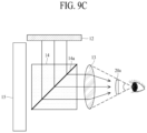
- FIGS. 9 A to 9 C relate to an electroluminescent display apparatus according to another aspect of the present disclosure and relate to a head-mounted display (HMD) apparatus.
- FIG. 9 A is a schematic perspective view
- FIG. 9 B is a schematic plan view of a virtual reality (VR) structure
- FIG. 9 C is a schematic cross-sectional view of an augmented reality (AR) structure.
- VR virtual reality
- AR augmented reality
- the HMD apparatus may include an accommodating case 10 and a head-mounted band 30 .
- the accommodating case 10 may accommodate elements such as a display apparatus, a lens array, and an eyepiece lens.
- the head-mounted band 30 may be fixed to the accommodating case 10 .
- the head-mounted band 30 is illustrated as being provided to surround an upper surface of both side surfaces of a user, but is not limited thereto.
- the head-mounted band 30 may fix the HMD apparatus to a head of a user and may be replaced by a glasses frame type structure or a helmet type structure.
- an HMD apparatus having the VR structure according to the present disclosure may include a left-eye display apparatus 12 , a right-eye display apparatus 11 , a lens array 13 , a left-eye eyepiece lens 20 a , and a right-eye eyepiece lens 20 b.
- the left-eye display apparatus 12 , the right-eye display apparatus 11 , the lens array 13 , the left-eye eyepiece lens 20 a , and the right-eye eyepiece lens 20 b may be accommodated into the accommodating case 10 .
- the left-eye display apparatus 12 and the right-eye display apparatus 11 may display the same image, and in this case, a user may watch a two-dimensional (2D) image.
- the left-eye display apparatus 12 may display a left-eye image
- the right-eye display apparatus 11 may display a right-eye image.
- Each of the left-eye display apparatus 12 and the right-eye display apparatus 11 may be configured as the electroluminescent display apparatus as explained above. In this case, an upper portion corresponding to a surface displaying an image may face the lens array 13 .
- the lens array 13 may be spaced apart from each of the left-eye eyepiece lens 20 a and the left-eye display apparatus 12 and may be provided between the left-eye eyepiece lens 20 a and the left-eye display apparatus 12 . That is, the lens array 13 may be disposed in front of the left-eye eyepiece lens 20 a and behind the left-eye display apparatus 12 . Also, the lens array 13 may be spaced apart from each of the right-eye eyepiece lens 20 b and the right-eye display apparatus 11 and may be provided between the right-eye eyepiece lens 20 b and the right-eye display apparatus 11 . That is, the lens array 13 may be disposed in front of the right-eye eyepiece lens 20 b and behind the right-eye display apparatus 11 .
- the lens array 13 may be a micro-lens array.
- the lens array 13 may be replaced by a pin hole array.
- an image displayed by the left-eye display apparatus 12 or the right-eye display apparatus 11 may be zoomed in by a certain magnification, and thus, a zoomed-in image may be seen by a user.
- a left eye LE of a user may be located at the left-eye eyepiece lens 20 a
- a right eye RE of the user may be located at the right-eye eyepiece lens 20 b.
- an HMD apparatus having the AR structure according to the present disclosure may include a left-eye display apparatus 12 , a lens array 13 , a left-eye eyepiece lens 20 a , a transmissive reflection part 14 , and a transmissive window 15 .
- a left-eye display apparatus 12 may include a left-eye display apparatus 12 , a lens array 13 , a left-eye eyepiece lens 20 a , a transmissive reflection part 14 , and a transmissive window 15 .
- FIG. 9 C for convenience, only left-eye elements are illustrated, and right-eye elements may be the same as the left-eye elements.
- the left-eye display apparatus 12 , the lens array 13 , the left-eye eyepiece lens 20 a , the transmissive reflection part 14 , and the transmissive window 15 may be accommodated into the accommodating case 10 .
- the left-eye display apparatus 12 may be disposed in one side (for example, an upper side) of the transmissive reflection part 14 without covering the transmissive window 15 . Therefore, the left-eye display apparatus 12 may provide an image to the transmissive reflection part 14 without covering an external background seen through the transmissive window 15 .
- the left-eye display apparatus 12 may be configured as the electroluminescent display apparatus as explained above. In this case, an upper portion corresponding to a surface displaying an image may face the transmissive reflection part 14 .
- the lens array 13 may be provided between the left-eye eyepiece lens 20 a and the transmissive reflection part 14 .
- the left eye of the user may be located at the left-eye eyepiece lens 20 a.
- the transmissive reflection part 14 may be disposed between the lens array 13 and the transmissive window 15 .
- the transmissive reflection part 14 may include a reflection surface 14 a which transmits a portion of light and reflects the other portion of the light.
- the reflection surface 14 a may be provided so that an image displayed by the left-eye display apparatus 12 travels to the lens array 13 . Accordingly, the user may see, through the transmissive window 15 , all of the external background and the image displayed by the left-eye display apparatus 12 . That is, the user may see one image which includes a real background and a virtual image, and thus, AR may be implemented.
- the transmissive window 15 may be disposed in front of the transmissive reflection part 14 .
- the trench is formed at the boundary between the subpixels, a portion of the light emitting layer in one subpixel and a portion of the light emitting layer in another subpixel adjacent thereto are disconnected from each other in the trench, whereby a leakage current may be prevented from occurring between the adjacent subpixels, and deterioration of image quality due to the leakage current may be avoided.
- the hole injection layer of the first stack is provided to be discontinuous in the first and second trenches, whereby a leakage current may be prevented from occurring between the subpixels disposed to be adjacent to each other.
- the charge generation layer is provided to be discontinuous in the first trench, whereby a leakage current may be prevented from occurring between the subpixels disposed to be adjacent to each other.
- the hole injection layer is discontinuous in the second trench, even though a short occurs between the charge generation layer and the hole injection layer in the first trench, the charge generation layer and the hole injection layer are not connected to each other in each subpixel, whereby desired light emission may be obtained in the light emitting layer.
- the first stack and the charge generation layer may be discontinuous in the first trench.
- the second pore since the second pore is extended from the inside of the second trench to the outside above the second trench, the hole injection layer of the first stack may be discontinuous in the first trench.
Landscapes
- Physics & Mathematics (AREA)
- Optics & Photonics (AREA)
- Engineering & Computer Science (AREA)
- Microelectronics & Electronic Packaging (AREA)
- General Physics & Mathematics (AREA)
- Geometry (AREA)
- Electroluminescent Light Sources (AREA)
Abstract
Description
Claims (20)
Applications Claiming Priority (2)
| Application Number | Priority Date | Filing Date | Title |
|---|---|---|---|
| KR10-2020-0180790 | 2020-12-22 | ||
| KR1020200180790A KR102860230B1 (en) | 2020-12-22 | 2020-12-22 | Electroluminescent Display Device |
Publications (2)
| Publication Number | Publication Date |
|---|---|
| US20220199709A1 US20220199709A1 (en) | 2022-06-23 |
| US12048218B2 true US12048218B2 (en) | 2024-07-23 |
Family
ID=82022419
Family Applications (1)
| Application Number | Title | Priority Date | Filing Date |
|---|---|---|---|
| US17/551,837 Active 2042-05-06 US12048218B2 (en) | 2020-12-22 | 2021-12-15 | Electroluminescent display device comprising trenches between adjacent subpixels |
Country Status (2)
| Country | Link |
|---|---|
| US (1) | US12048218B2 (en) |
| KR (1) | KR102860230B1 (en) |
Families Citing this family (3)
| Publication number | Priority date | Publication date | Assignee | Title |
|---|---|---|---|---|
| WO2024065616A1 (en) * | 2022-09-30 | 2024-04-04 | 京东方科技集团股份有限公司 | Display panel and display device |
| KR20250101399A (en) * | 2023-12-27 | 2025-07-04 | 엘지디스플레이 주식회사 | Display device |
| CN118973318B (en) * | 2024-07-26 | 2026-01-06 | 京东方科技集团股份有限公司 | Display substrate and display device |
Citations (3)
| Publication number | Priority date | Publication date | Assignee | Title |
|---|---|---|---|---|
| US20190181368A1 (en) * | 2017-11-03 | 2019-06-13 | Lg Display Co., Ltd. | Electroluminescent display device |
| US20200135818A1 (en) * | 2018-10-29 | 2020-04-30 | Lg Display Co., Ltd. | Electroluminescent display apparatus |
| US20200144342A1 (en) * | 2018-11-02 | 2020-05-07 | Lg Display Co., Ltd. | Electroluminescent display apparatus |
Family Cites Families (2)
| Publication number | Priority date | Publication date | Assignee | Title |
|---|---|---|---|---|
| JP6957294B2 (en) * | 2017-09-28 | 2021-11-02 | キヤノン株式会社 | Display devices, electronic devices, and manufacturing methods for display devices |
| KR102875730B1 (en) * | 2018-07-31 | 2025-10-24 | 엘지디스플레이 주식회사 | Electroluminescent Display Device |
-
2020
- 2020-12-22 KR KR1020200180790A patent/KR102860230B1/en active Active
-
2021
- 2021-12-15 US US17/551,837 patent/US12048218B2/en active Active
Patent Citations (3)
| Publication number | Priority date | Publication date | Assignee | Title |
|---|---|---|---|---|
| US20190181368A1 (en) * | 2017-11-03 | 2019-06-13 | Lg Display Co., Ltd. | Electroluminescent display device |
| US20200135818A1 (en) * | 2018-10-29 | 2020-04-30 | Lg Display Co., Ltd. | Electroluminescent display apparatus |
| US20200144342A1 (en) * | 2018-11-02 | 2020-05-07 | Lg Display Co., Ltd. | Electroluminescent display apparatus |
Also Published As
| Publication number | Publication date |
|---|---|
| KR20220090025A (en) | 2022-06-29 |
| US20220199709A1 (en) | 2022-06-23 |
| KR102860230B1 (en) | 2025-09-15 |
Similar Documents
| Publication | Publication Date | Title |
|---|---|---|
| US11302757B2 (en) | Electroluminescent display apparatus including plurality of grooves overlapping bank hole between adjacent subpixels | |
| US11088339B2 (en) | Electroluminescent display device | |
| US11211588B2 (en) | Electroluminescent display device | |
| US11302885B2 (en) | Electroluminescent display device | |
| US11903231B2 (en) | Electroluminescent display device | |
| US11362147B2 (en) | Display device | |
| US12048218B2 (en) | Electroluminescent display device comprising trenches between adjacent subpixels | |
| US12274112B2 (en) | Electroluminescent display device | |
| US10840316B2 (en) | Electroluminescent display apparatus | |
| US12507533B2 (en) | Electroluminescent display apparatus | |
| US11158696B2 (en) | Electroluminescent display apparatus | |
| US12029066B2 (en) | Electroluminescent display device including reflective layer | |
| US11189678B2 (en) | Electroluminescent display apparatus and display apparatus | |
| KR20200014176A (en) | Display device | |
| KR102710943B1 (en) | Electroluminescent Display Device | |
| KR20220096851A (en) | Display apparatus |
Legal Events
| Date | Code | Title | Description |
|---|---|---|---|
| FEPP | Fee payment procedure |
Free format text: ENTITY STATUS SET TO UNDISCOUNTED (ORIGINAL EVENT CODE: BIG.); ENTITY STATUS OF PATENT OWNER: LARGE ENTITY |
|
| AS | Assignment |
Owner name: LG DISPLAY CO., LTD., KOREA, REPUBLIC OF Free format text: ASSIGNMENT OF ASSIGNORS INTEREST;ASSIGNORS:BAIK, SEUNGMIN;JUN, CHANGHWA;REEL/FRAME:058561/0932 Effective date: 20211101 |
|
| STPP | Information on status: patent application and granting procedure in general |
Free format text: DOCKETED NEW CASE - READY FOR EXAMINATION |
|
| STPP | Information on status: patent application and granting procedure in general |
Free format text: NON FINAL ACTION MAILED |
|
| STPP | Information on status: patent application and granting procedure in general |
Free format text: RESPONSE TO NON-FINAL OFFICE ACTION ENTERED AND FORWARDED TO EXAMINER |
|
| STPP | Information on status: patent application and granting procedure in general |
Free format text: FINAL REJECTION MAILED |
|
| STPP | Information on status: patent application and granting procedure in general |
Free format text: DOCKETED NEW CASE - READY FOR EXAMINATION |
|
| STPP | Information on status: patent application and granting procedure in general |
Free format text: NON FINAL ACTION MAILED |
|
| STPP | Information on status: patent application and granting procedure in general |
Free format text: RESPONSE TO NON-FINAL OFFICE ACTION ENTERED AND FORWARDED TO EXAMINER |
|
| STPP | Information on status: patent application and granting procedure in general |
Free format text: NOTICE OF ALLOWANCE MAILED -- APPLICATION RECEIVED IN OFFICE OF PUBLICATIONS |
|
| STPP | Information on status: patent application and granting procedure in general |
Free format text: PUBLICATIONS -- ISSUE FEE PAYMENT VERIFIED |
|
| STCF | Information on status: patent grant |
Free format text: PATENTED CASE |