US12047002B2 - Multiphase voltage regulator variable phase control stability - Google Patents
Multiphase voltage regulator variable phase control stability Download PDFInfo
- Publication number
- US12047002B2 US12047002B2 US17/567,018 US202117567018A US12047002B2 US 12047002 B2 US12047002 B2 US 12047002B2 US 202117567018 A US202117567018 A US 202117567018A US 12047002 B2 US12047002 B2 US 12047002B2
- Authority
- US
- United States
- Prior art keywords
- controller
- power stages
- adjust
- ripple resistance
- resistance
- Prior art date
- Legal status (The legal status is an assumption and is not a legal conclusion. Google has not performed a legal analysis and makes no representation as to the accuracy of the status listed.)
- Active, expires
Links
- 230000004044 response Effects 0.000 abstract description 23
- 238000000034 method Methods 0.000 abstract description 12
- 230000008569 process Effects 0.000 description 8
- 238000010586 diagram Methods 0.000 description 6
- 239000003990 capacitor Substances 0.000 description 3
- 230000008859 change Effects 0.000 description 2
- 230000005669 field effect Effects 0.000 description 2
- 239000000463 material Substances 0.000 description 2
- 238000012986 modification Methods 0.000 description 2
- 230000004048 modification Effects 0.000 description 2
- 230000003213 activating effect Effects 0.000 description 1
- 230000008901 benefit Effects 0.000 description 1
- 230000033228 biological regulation Effects 0.000 description 1
- 238000006243 chemical reaction Methods 0.000 description 1
- 230000003247 decreasing effect Effects 0.000 description 1
- 238000002347 injection Methods 0.000 description 1
- 239000007924 injection Substances 0.000 description 1
- 238000013507 mapping Methods 0.000 description 1
- 238000005259 measurement Methods 0.000 description 1
Images


Classifications
-
- H—ELECTRICITY
- H02—GENERATION; CONVERSION OR DISTRIBUTION OF ELECTRIC POWER
- H02M—APPARATUS FOR CONVERSION BETWEEN AC AND AC, BETWEEN AC AND DC, OR BETWEEN DC AND DC, AND FOR USE WITH MAINS OR SIMILAR POWER SUPPLY SYSTEMS; CONVERSION OF DC OR AC INPUT POWER INTO SURGE OUTPUT POWER; CONTROL OR REGULATION THEREOF
- H02M3/00—Conversion of DC power input into DC power output
- H02M3/02—Conversion of DC power input into DC power output without intermediate conversion into AC
- H02M3/04—Conversion of DC power input into DC power output without intermediate conversion into AC by static converters
- H02M3/10—Conversion of DC power input into DC power output without intermediate conversion into AC by static converters using discharge tubes with control electrode or semiconductor devices with control electrode
- H02M3/145—Conversion of DC power input into DC power output without intermediate conversion into AC by static converters using discharge tubes with control electrode or semiconductor devices with control electrode using devices of a triode or transistor type requiring continuous application of a control signal
- H02M3/155—Conversion of DC power input into DC power output without intermediate conversion into AC by static converters using discharge tubes with control electrode or semiconductor devices with control electrode using devices of a triode or transistor type requiring continuous application of a control signal using semiconductor devices only
- H02M3/156—Conversion of DC power input into DC power output without intermediate conversion into AC by static converters using discharge tubes with control electrode or semiconductor devices with control electrode using devices of a triode or transistor type requiring continuous application of a control signal using semiconductor devices only with automatic control of output voltage or current, e.g. switching regulators
- H02M3/158—Conversion of DC power input into DC power output without intermediate conversion into AC by static converters using discharge tubes with control electrode or semiconductor devices with control electrode using devices of a triode or transistor type requiring continuous application of a control signal using semiconductor devices only with automatic control of output voltage or current, e.g. switching regulators including plural semiconductor devices as final control devices for a single load
-
- G—PHYSICS
- G05—CONTROLLING; REGULATING
- G05F—SYSTEMS FOR REGULATING ELECTRIC OR MAGNETIC VARIABLES
- G05F1/00—Automatic systems in which deviations of an electric quantity from one or more predetermined values are detected at the output of the system and fed back to a device within the system to restore the detected quantity to its predetermined value or values, i.e. retroactive systems
- G05F1/10—Regulating voltage or current
- G05F1/46—Regulating voltage or current wherein the variable actually regulated by the final control device is DC
- G05F1/56—Regulating voltage or current wherein the variable actually regulated by the final control device is DC using semiconductor devices in series with the load as final control devices
- G05F1/575—Regulating voltage or current wherein the variable actually regulated by the final control device is DC using semiconductor devices in series with the load as final control devices characterised by the feedback circuit
-
- H—ELECTRICITY
- H02—GENERATION; CONVERSION OR DISTRIBUTION OF ELECTRIC POWER
- H02M—APPARATUS FOR CONVERSION BETWEEN AC AND AC, BETWEEN AC AND DC, OR BETWEEN DC AND DC, AND FOR USE WITH MAINS OR SIMILAR POWER SUPPLY SYSTEMS; CONVERSION OF DC OR AC INPUT POWER INTO SURGE OUTPUT POWER; CONTROL OR REGULATION THEREOF
- H02M1/00—Details of apparatus for conversion
- H02M1/0003—Details of control, feedback or regulation circuits
- H02M1/0025—Arrangements for modifying reference values, feedback values or error values in the control loop of a converter
-
- H—ELECTRICITY
- H02—GENERATION; CONVERSION OR DISTRIBUTION OF ELECTRIC POWER
- H02M—APPARATUS FOR CONVERSION BETWEEN AC AND AC, BETWEEN AC AND DC, OR BETWEEN DC AND DC, AND FOR USE WITH MAINS OR SIMILAR POWER SUPPLY SYSTEMS; CONVERSION OF DC OR AC INPUT POWER INTO SURGE OUTPUT POWER; CONTROL OR REGULATION THEREOF
- H02M1/00—Details of apparatus for conversion
- H02M1/08—Circuits specially adapted for the generation of control voltages for semiconductor devices incorporated in static converters
- H02M1/088—Circuits specially adapted for the generation of control voltages for semiconductor devices incorporated in static converters for the simultaneous control of series or parallel connected semiconductor devices
-
- H—ELECTRICITY
- H02—GENERATION; CONVERSION OR DISTRIBUTION OF ELECTRIC POWER
- H02M—APPARATUS FOR CONVERSION BETWEEN AC AND AC, BETWEEN AC AND DC, OR BETWEEN DC AND DC, AND FOR USE WITH MAINS OR SIMILAR POWER SUPPLY SYSTEMS; CONVERSION OF DC OR AC INPUT POWER INTO SURGE OUTPUT POWER; CONTROL OR REGULATION THEREOF
- H02M3/00—Conversion of DC power input into DC power output
- H02M3/02—Conversion of DC power input into DC power output without intermediate conversion into AC
- H02M3/04—Conversion of DC power input into DC power output without intermediate conversion into AC by static converters
- H02M3/10—Conversion of DC power input into DC power output without intermediate conversion into AC by static converters using discharge tubes with control electrode or semiconductor devices with control electrode
- H02M3/145—Conversion of DC power input into DC power output without intermediate conversion into AC by static converters using discharge tubes with control electrode or semiconductor devices with control electrode using devices of a triode or transistor type requiring continuous application of a control signal
- H02M3/155—Conversion of DC power input into DC power output without intermediate conversion into AC by static converters using discharge tubes with control electrode or semiconductor devices with control electrode using devices of a triode or transistor type requiring continuous application of a control signal using semiconductor devices only
- H02M3/156—Conversion of DC power input into DC power output without intermediate conversion into AC by static converters using discharge tubes with control electrode or semiconductor devices with control electrode using devices of a triode or transistor type requiring continuous application of a control signal using semiconductor devices only with automatic control of output voltage or current, e.g. switching regulators
- H02M3/158—Conversion of DC power input into DC power output without intermediate conversion into AC by static converters using discharge tubes with control electrode or semiconductor devices with control electrode using devices of a triode or transistor type requiring continuous application of a control signal using semiconductor devices only with automatic control of output voltage or current, e.g. switching regulators including plural semiconductor devices as final control devices for a single load
- H02M3/1584—Conversion of DC power input into DC power output without intermediate conversion into AC by static converters using discharge tubes with control electrode or semiconductor devices with control electrode using devices of a triode or transistor type requiring continuous application of a control signal using semiconductor devices only with automatic control of output voltage or current, e.g. switching regulators including plural semiconductor devices as final control devices for a single load with a plurality of power processing stages connected in parallel
-
- H—ELECTRICITY
- H02—GENERATION; CONVERSION OR DISTRIBUTION OF ELECTRIC POWER
- H02M—APPARATUS FOR CONVERSION BETWEEN AC AND AC, BETWEEN AC AND DC, OR BETWEEN DC AND DC, AND FOR USE WITH MAINS OR SIMILAR POWER SUPPLY SYSTEMS; CONVERSION OF DC OR AC INPUT POWER INTO SURGE OUTPUT POWER; CONTROL OR REGULATION THEREOF
- H02M1/00—Details of apparatus for conversion
- H02M1/0003—Details of control, feedback or regulation circuits
- H02M1/0009—Devices or circuits for detecting current in a converter
-
- Y—GENERAL TAGGING OF NEW TECHNOLOGICAL DEVELOPMENTS; GENERAL TAGGING OF CROSS-SECTIONAL TECHNOLOGIES SPANNING OVER SEVERAL SECTIONS OF THE IPC; TECHNICAL SUBJECTS COVERED BY FORMER USPC CROSS-REFERENCE ART COLLECTIONS [XRACs] AND DIGESTS
- Y02—TECHNOLOGIES OR APPLICATIONS FOR MITIGATION OR ADAPTATION AGAINST CLIMATE CHANGE
- Y02B—CLIMATE CHANGE MITIGATION TECHNOLOGIES RELATED TO BUILDINGS, e.g. HOUSING, HOUSE APPLIANCES OR RELATED END-USER APPLICATIONS
- Y02B70/00—Technologies for an efficient end-user side electric power management and consumption
- Y02B70/10—Technologies improving the efficiency by using switched-mode power supplies [SMPS], i.e. efficient power electronics conversion e.g. power factor correction or reduction of losses in power supplies or efficient standby modes
Definitions
- the present disclosure relates in general to operations of power converters. More specifically, the present disclosure relates to controlling a stability of a multiphase voltage regulator.
- DC-to-DC voltage conversion may be performed by switching voltage regulators or power converters to convert a voltage from a higher level to a lower level that may be required by a load.
- An example architecture may distribute the higher voltage to multiple voltage regulators or power stages, and each voltage regulator may produce a same or different voltages for one or more loads.
- a switching voltage regulator may use two or more power transistors to convert energy from one voltage to another voltage.
- One example of such a switching voltage regulator may be the Buck Regulator, which typically switches a pair of power transistors to produce a square-wave at a common node between the pair of power transistors.
- the produced square-wave may be smoothed out using a resonant circuit (e.g., an inductor-capacitor (LC) circuit) to produce a desired voltage for a load.
- a resonant circuit e.g., an inductor-capacitor (LC) circuit
- a feedback control loop may be configured to control a duty-cycle of the produced square-wave and a resulting value of an output voltage of the voltage converter.
- An example voltage regulator architecture may be a multiphase voltage regulator including multiple power stages, and the power stages can be referred to as phases.
- Each power stage includes a pair of power transistors (e.g., field-effect transistors (FET)), an inductor and a output capacitor connected to the power stage's output, and a controller.
- the voltage output from each activated power stage can be interleaved at an output node to produce an overall output voltage.
- the phases are connected in parallel, and different number of power stages can be activated (e.g., switched on) to output different overall output voltages, thus providing different power levels to a load.
- each power stage can measure parameters (e.g., inductor current and temperature) between the output node and the power stage's output. The measured parameters can be fed back to a master controller connected to the multiple power stages, and can be used by the master controller to maintain satisfactory performance level of the overall system and to determine optimal number of power stages to be activated.
- parameters e.g., inductor current
- an apparatus for operating a multiphase voltage regulator is generally described.
- a controller can be connected to a plurality of power stages in the multiphase voltage regulator.
- the controller can be configured to detect a number of activated power stages among the plurality of power stages.
- the controller can be further configured to adjust a gain of a current sense feedback loop of the controller to control a load-transient response of the apparatus. The adjustment of the gain can be based on the number of activated power stages.
- a multiphase voltage regulator system in another embodiment, can include a plurality of power stages and a controller connected to the plurality of power stages.
- the controller can be configured to detect a number of activated power stages among the plurality of power stages.
- the controller can be configured to adjust a gain of a current sense feedback loop of the controller to control a load-transient response of the system. The adjustment of the gain can be based on the number of activated power stages.
- a method for operating a multiphase voltage regulator can include detecting, by a controller, a number of activated power stages among the plurality of power stages.
- the controller can be connected to a plurality of power stages in the multiphase voltage regulator.
- the method can further include adjusting, by the controller, a gain of a current sense feedback loop of the controller to control a load-transient response of the multiphase voltage regulator. The adjustment of the gain can be based on the number of activated power stages.
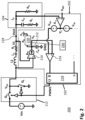
- FIG. 1 is a diagram showing an example system that can implement multiphase voltage regulator variable phase count stability in one embodiment.
- FIG. 2 is a diagram showing additional details of the system of FIG. 1 in one embodiment.
- FIG. 3 is a diagram showing a result of an implementation of multiphase voltage regulator variable phase count stability in one embodiment.
- FIG. 4 is a flowchart of an example process that may implement multiphase voltage regulator variable phase count stability according to an embodiment of the disclosure.
- FIG. 1 is a diagram showing an example system that can implement multiphase voltage regulator variable phase count stability in one embodiment.
- the system 100 may be an apparatus implementing a multiphase voltage regulator including a controller 102 and at least one voltage regulators or power stages, such as a power stage 110 and a power stage 120 .
- the controller 102 may be a master controller, or a multiphase controller, and the power stages 110 , 120 may include DC-DC converters.
- the controller 102 may be configured to control the power stage 110 using a pulse width modulation (PWM) signal PWM 1 being sent from the controller 102 to a PWM pin of the power stage 110 .
- the power stage 110 may include a power transistor pair 112 and a power stage controller 114 .
- the power transistor pair 112 may include a high side field-effect transistor (FET) and a low side FET.
- the PWM signal PWM 1 can be a control signal that switches the power transistor pair 112 to convert an input voltage Vin into an output voltage V 1 .
- the controller 102 may be configured to control the power stage 120 using another PWM signal PWM 2 being sent from the controller 102 to a PWM pin of the power stage 120 .
- the power stage 120 may include a power transistor pair 122 and a power stage controller 124 .
- the power transistor pair 122 may include a high side FET and a low side FET.
- the PWM signal PWM 2 can be a control signal that switches the power transistor pair 122 to convert the input voltage Vin into an output voltage V 2 .
- the output voltages V 1 and V 2 can be combined or interleaved at a node 128 to produce an overall output voltage Vout to a load 104 .
- the voltage levels of V 1 and V 2 can be the same as Vout, but may be staggered or out of phase from one another.
- the power stages 110 , 120 may be current-sourced devices, voltage-sourced devices, or a device implementing both current and voltage-sourced control.
- the power stages 110 , 120 may be smart power stage (SPS) devices configured to perform voltage regulation with additional features such as feedback control based on feedback voltage and/or feedback current, or other parameters such as temperature, measured at the outputs of the power stages in the system 100 .
- SPS smart power stage
- the power stages 110 , 120 can provide operating temperatures of the power stages 110 , 120 from the TMON pin of the power stages 110 , 120 to a TSEN pin of the controller 102 .
- the power stages 110 , 120 can measure inductor currents i L1 , i L2 , of the inductors L 1 , L 2 , respectively.
- the power stages 110 , 120 can provide the measured inductor current to the controller 102 from their IMON pins of the power stages 110 , 120 to the ISEN_1 and ISEN_2 pins of the controller 102 , respectively. Further, a measurement of the output voltage Vout can be fed back to the controller 102 (e.g., received at a VSENSE pin of the controller 102 ) for various control applications.
- the power stage controllers 114 , 124 , of the power stages 110 , 120 can be configured to process the measured parameters of the power stages 110 , 120 , respectively, before providing the measured parameters to the controller 102 .
- the power stage controllers 114 , 124 can amplify and/or calibrate the measured parameters prior to providing them to the controller 102 .
- the power stage controllers 114 , 124 can also include drivers configured to drive the power transistor pairs 112 , 122 of the power stages 110 , 120 , respectively.
- the controller 102 can be configured to use feedback signals such as the sensed output voltage Vout, sensed current (e.g., the currents i L1 , i L2 , or current proportional to i L1 , i L2 ), and/or temperature information (e.g., operating temperature) to control and maintain the performance of the system 100 at a satisfactory level (e.g., within predefined specifications). For example, if the sensed current returned from the power stages 110 , 120 indicates the load 104 is not drawing as much current as expected, the controller 102 can deactivate one or more power stages in the system 100 to reduce an overall power consumption of the system 100 .
- sensed current e.g., the currents i L1 , i L2 , or current proportional to i L1 , i L2
- temperature information e.g., operating temperature
- the controller 102 can enable the power stages in the system 100 individually via an enable pin EN of the controller 102 and an enable pin EN of each of the power stages 110 , 120 .
- the enable pin EN of the controller 102 can be connected to the enable pins EN of the power stages 110 , 120 using a specific bus (e.g., a single wire or single trace).
- the controller 102 can be a microcontroller including hardware components such as integrated circuits (IC), memory devices, and other hardware and circuit components.
- the controller 102 can include a modulator 130 configured to generate PWM signals for the power stages connected to the controller 102 , such as the PWM signal PWM 1 and the PWM signal PWM 2 .
- the modulator 130 can receive the output voltage Vout at a VSENSE pin of the controller 102 , or a feedback voltage signal that may be a sensed or proportional signal indicative of Vout.
- the controller 102 can include a current synthesizer 140 configured to receive the inductor currents i L1 , i L2 , etc., sensed from the output inductors of the power stages in the system 100 .
- the current synthesizer 140 can be configured to simulate or synthesized the inductor currents of power stages 110 , 120 , based on the sensed inductor currents i L1 , i L2 , respectively.
- An output of the current synthesizer 140 e.g., simulated or synthesized current
- PWM 1 , PWM 2 can be provided to the modulator 130 to generate and/or adjust the PWM signals PWM 1 , PWM 2 .
- the inductor current of the inductors can ramp up and ramp down repeatedly.
- the power consumption by the system 100 can increase as more power stages are activated. If the load 104 needs to draw more power, more power stages can be activated—referred to as phase-add. If the load 104 can draw less power, less power stages can be activated—referred to as phase-drop.
- the phase-add and phase-drop to activate different number of power stages can create load fluctuations, causing unstable load-transient response and sometimes slow load-transient response.
- the controller 102 can be integrated with specific hardware that can allow the controller 102 to dynamically adjust a gain of the controller 102 and/or the current synthesizer to control the load-transient response in response to phase-add or phase-drop processes.
- FIG. 2 is a diagram showing additional details of the system 100 of FIG. 1 in one embodiment.
- a circuit 200 includes one or more portions of the controller 102 , the power stage 110 , the load 104 , and other components of the system 100 of FIG. 1 , are shown in FIG. 2 .
- the details of the power stage 110 shown in FIG. 2 and corresponding descriptions are also applicable to the power stage 120 in FIG. 1 , and/or other power stages in the system 100 connected to the controller 102 .
- the power transistor pair 112 of the power stage 110 can include a high-side transistor Q U and a low-side transistor Q L .
- the high-side transistor Q U and the low-side transistor Q L can be FETs.
- the controller 102 can drive the power transistor pair 112 to alternately switch on and switch off the high-side transistor Q U and the low-side transistor Q L . For example, when Q U is on, Q L is off, and vice versa.
- a phase voltage V PH can be outputted from a node between the high-side transistor Q U and the low-side transistor Q L as a result of the switching driven by the PWM 1 signal.
- the phase voltage V PH can create the inductor current i L1 across the inductor L 1 .
- the inductance of L 1 and an inherent resistance R L of the inductor L 1 can cause the output voltage V 1 to be generated by the power stage 110 .
- the voltage V 1 can be interleaved with other output voltages from other power stages at the node 128 to create the overall output voltage Vout for the load 104 .
- the current synthesizer 140 of the controller 102 can include a transconductance amplifier 210 having a transconductance gain g M .
- the phase voltage V PH can be received at a non-inverting input of the transconductance amplifier 210
- the output voltage V 1 can be received at an inverting input of the transconductance amplifier 210 .
- An output of the transconductance amplifier 210 can be coupled to a ripple node 212 .
- a capacitor having ripple capacitance C R can be coupled between the ripple node 212 and ground GND.
- a resistor circuit block 230 having a ripple resistance R R can be coupled between the ripple node 212 and an internal reference or bias voltage V X .
- a ripple voltage V R can be developed from the ripple node 212 based on an output current from the transconductance amplifier 210 , the capacitance C R , the internal reference voltage V X , and the ripple resistance R R .
- the internal reference voltage V X can be injected into the ripple node 212 to control a stability of the ripple current V R .
- the transconductance amplifier 210 can be configured to generate its output current to be proportional to the voltage measured across the inductor L 1 (e.g., difference between V PH and V 1 ), in order for the ripple voltage V R to replicate the ripple current through the inductor L 1 .
- the replicated current can be a simulated or synthetic current being outputted by the current synthesizer 140 .
- the injection of V X into the ripple node 212 with the application of the ripple resistance R R , can introduce an offset to the output current from the transconductance amplifier 210 .
- the introduced offset can be the internal reference voltage V X .
- the internal reference voltage V X can be a midpoint voltage, a functional zero, a voltage representing zero for the corresponding phase or power stage (e.g., in this example, power stage 110 ), etc.
- the controller 102 can further include a comparator 216 .
- the ripple voltage V R can be received by a non-inverting input of the comparator 216
- a positive window voltage V W+ can be received by an inverting input of the comparator 216 .
- the positive window voltage V W+ can be based on a control or reference voltage V REF .
- An output of the comparator 216 is provided to a reset (R) terminal of a SR latch 218 in the controller 102 .
- the SR latch 218 can be a part of the modulator 130 shown in FIG. 1 .
- the SR latch 218 can output the PWM 1 signal from an output (Q) terminal of the SR latch 218 .
- the transconductance gain g M can be a gain of a currents sense feedback loop that includes a path from the nodes across inductor L 1 to SR latch 218 .
- An adjustment to transconductance gain g M can be an adjustment to this current sense feedback loop.
- the ripple resistance R R can be increased by configuring the resistor circuit block 230 .
- the gain g M can vary inversely with the value of ripple resistance R R .
- the gain g M can increase in response to a decrease in ripple resistance R R .
- a speed of the load-transient response of the system 100 can be improved (e.g., increased speed) because the decreased ripple resistance R R can lower a voltage drop for the load-transient response.
- the resistor circuit block 230 can include a variable resistor (e.g., digital potentiometer).
- the controller 102 can provide signals of different voltage levels to the variable resistor to change the ripple resistance R R .
- the resistor circuit block 230 can include a plurality of resistors.
- the controller 102 can activate and deactivate different numbers of resistors to change the ripple resistance R R .
- a plurality of resistors in the resistor circuit block 230 can be connected in parallel, and each resistor can be connected to a switch.
- the controller 102 can be configured to open and close different number of switches connected to the plurality of resistors to adjust the value of R R .
- the resistor circuit block 230 includes multiple resistors that can be activated or deactivated, the multiple resistors can have the same or different resistance values to provide flexible adjustments of the value of ripple resistance R R .
- the controller 102 can include a memory device configured to store associations 240 between different values of the ripple resistance R R and different numbers of activated power stages.
- the associations 240 can be stored as, for example, lookup tables or mappings.
- M can be equivalent to N such that there can be one value of ripple resistance R R for each number of activated power stages.
- M can be less than N such that there can be one value of ripple resistance R R for each group of activated power stages, where one group of activated power stages can include one or more power stage.
- the controller 102 can be configured to configure the resistor circuit block 230 based on the associations 240 .
- the controller 102 can detect a number of activated power stages. For example, the controller 102 can interpret the enable signal on being outputted on the EN pin of the controller 102 to identify which power stages, and how many power stages, are being activated. In one embodiment, based on the number of activated power stages, the controller 102 can refer to the associations 240 to configure the value of the ripple resistance R R . For example, in response to the associations 240 indicating four activated power stages is associated with a resistance value R 4 , the controller 102 can configure the resistor block to adjust the value of R R to R 4 .
- the controller 102 can be configured to adjust the value of the ripple resistance R R for all power stages that are activated. For example, if the system 100 includes N power stages, there can be N copies of the circuit 200 shown in FIG. 2 . If k out of N power stages are activated in the system 100 , the controller 102 can adjust the value of the ripple resistance R R for the k copies of circuit 200 . Further, the adjustment to the ripple resistance R R for all power stages can be the same. For example, the controller 102 can adjust the resistor circuit block 230 in the k copies of circuit 200 to have the same ripple resistance R R value.
- FIG. 3 is a diagram showing a result 300 of an implementation of multiphase voltage regulator variable phase count stability in one embodiment.
- a first curve labeled as “Original RR (200K)” is the load-transient response where the value of R R in FIG. 2 is fixed at 200 kiloohms (k ⁇ ).
- a second curve labeled as “modified RR (50K)” is the load-transient response where the value of R R in FIG. 2 is adjusted to 50 kiloohms (k ⁇ ).
- the load-transient response represented by the first curve and the second curve can be based on the same number of activated phases or power stages in the system 100 .
- a load-transient response based on a higher value of R R e.g., first curve becomes steady at a later time 304
- a load-transient response based on a lower value of R R second curve becomes steady at an earlier time 302 .
- FIG. 4 is a flowchart of an example process 400 that may implement multiphase voltage regulator variable phase count stability according to an embodiment of the disclosure.
- the process 400 can include one or more operations, actions, or functions as illustrated by one or more of blocks 402 , 404 , and 406 or 408 . Although illustrated as discrete blocks, various blocks can be divided into additional blocks, combined into fewer blocks, eliminated, performed in different order, or performed in parallel, depending on the desired implementation.
- the process 400 can be performed by a controller (e.g., controller 102 in FIG. 1 and FIG. 2 ) connected to a plurality of power stages in a multiphase voltage regulator.
- the process 400 can begin at block 402 .
- the controller can detect a number of activated power stages among the plurality of power stages.
- a gain of the current synthesizer can increase in response to a decrease in the ripple resistance.
- the current synthesizer can correspond to a specific power stage among the activated power stages.
- the current synthesizer can simulate an inductor current of a specific power stage among the activated power stages.
- the process 400 can proceed from block 402 to block 404 .
- the controller can adjust a gain of a current sense feedback loop of the controller to control a load-transient response of the multiphase voltage regulator.
- the adjustment of the gain can be based on the number of activated power stages.
- the controller can adjust the gain by adjusting a ripple resistance in a current synthesizer of the controller.
- an increase of the gain can increase a speed of a load-transient response of the multiphase voltage regulator.
- the controller can adjust a gain of current sense feedback loops in other power stages among the activated power stages based on the number of activated power stages.
- the operation in the block 404 can be performed by performing either one of block 406 or block 408 .
- the controller can adjust the gain by activating a specific number of resistors in the current synthesizer.
- the controller can adjust the gain by adjusting a resistance of a variable resistor in the current synthesizer.
Landscapes
- Engineering & Computer Science (AREA)
- Power Engineering (AREA)
- Physics & Mathematics (AREA)
- Electromagnetism (AREA)
- General Physics & Mathematics (AREA)
- Radar, Positioning & Navigation (AREA)
- Automation & Control Theory (AREA)
- Dc-Dc Converters (AREA)
Abstract
Description
Claims (17)
Priority Applications (1)
| Application Number | Priority Date | Filing Date | Title |
|---|---|---|---|
| US17/567,018 US12047002B2 (en) | 2021-06-15 | 2021-12-31 | Multiphase voltage regulator variable phase control stability |
Applications Claiming Priority (2)
| Application Number | Priority Date | Filing Date | Title |
|---|---|---|---|
| US202163210575P | 2021-06-15 | 2021-06-15 | |
| US17/567,018 US12047002B2 (en) | 2021-06-15 | 2021-12-31 | Multiphase voltage regulator variable phase control stability |
Publications (2)
| Publication Number | Publication Date |
|---|---|
| US20220399813A1 US20220399813A1 (en) | 2022-12-15 |
| US12047002B2 true US12047002B2 (en) | 2024-07-23 |
Family
ID=84390542
Family Applications (1)
| Application Number | Title | Priority Date | Filing Date |
|---|---|---|---|
| US17/567,018 Active 2042-10-16 US12047002B2 (en) | 2021-06-15 | 2021-12-31 | Multiphase voltage regulator variable phase control stability |
Country Status (3)
| Country | Link |
|---|---|
| US (1) | US12047002B2 (en) |
| CN (1) | CN115483831A (en) |
| TW (1) | TW202301786A (en) |
Citations (7)
| Publication number | Priority date | Publication date | Assignee | Title |
|---|---|---|---|---|
| US20100085024A1 (en) * | 2008-10-02 | 2010-04-08 | Intersil Americas Inc. | Power supply controller with different steady state and transient response characteristics |
| US8004248B2 (en) * | 2006-05-30 | 2011-08-23 | Texas Instruments Incorporated | Systems and methods for multi-mode battery charging |
| US9342086B2 (en) * | 2014-08-27 | 2016-05-17 | Intersil Americas LLC | Current mode control modulator with combined control signals and improved dynamic range |
| US9374003B1 (en) * | 2010-06-23 | 2016-06-21 | Volterra Semiconductor LLC | Systems and methods for DC-to-DC converter control |
| US10054970B2 (en) * | 2016-01-27 | 2018-08-21 | Dialog Semiconductor (Uk) Limited | Adaptive gain control for voltage regulators |
| US10637266B2 (en) * | 2015-06-01 | 2020-04-28 | Intersil Americas LLC | Regulator with high speed nonlinear compensation |
| US10996249B2 (en) * | 2017-09-06 | 2021-05-04 | Johnson Controls Fire Protection LP | Software defined battery charger system and method |
-
2021
- 2021-12-31 US US17/567,018 patent/US12047002B2/en active Active
-
2022
- 2022-05-05 TW TW111116966A patent/TW202301786A/en unknown
- 2022-05-31 CN CN202210609595.5A patent/CN115483831A/en active Pending
Patent Citations (8)
| Publication number | Priority date | Publication date | Assignee | Title |
|---|---|---|---|---|
| US8004248B2 (en) * | 2006-05-30 | 2011-08-23 | Texas Instruments Incorporated | Systems and methods for multi-mode battery charging |
| US20100085024A1 (en) * | 2008-10-02 | 2010-04-08 | Intersil Americas Inc. | Power supply controller with different steady state and transient response characteristics |
| US9374003B1 (en) * | 2010-06-23 | 2016-06-21 | Volterra Semiconductor LLC | Systems and methods for DC-to-DC converter control |
| US9407145B1 (en) * | 2010-06-23 | 2016-08-02 | Volterra Semiconductor LLC | Systems and methods for DC-to-DC converter control |
| US9342086B2 (en) * | 2014-08-27 | 2016-05-17 | Intersil Americas LLC | Current mode control modulator with combined control signals and improved dynamic range |
| US10637266B2 (en) * | 2015-06-01 | 2020-04-28 | Intersil Americas LLC | Regulator with high speed nonlinear compensation |
| US10054970B2 (en) * | 2016-01-27 | 2018-08-21 | Dialog Semiconductor (Uk) Limited | Adaptive gain control for voltage regulators |
| US10996249B2 (en) * | 2017-09-06 | 2021-05-04 | Johnson Controls Fire Protection LP | Software defined battery charger system and method |
Also Published As
| Publication number | Publication date |
|---|---|
| CN115483831A (en) | 2022-12-16 |
| US20220399813A1 (en) | 2022-12-15 |
| TW202301786A (en) | 2023-01-01 |
Similar Documents
| Publication | Publication Date | Title |
|---|---|---|
| US8120346B2 (en) | Methods and apparatus for current sensing | |
| US11581796B2 (en) | Pulse width modulation controllers for hybrid converters | |
| US8044650B2 (en) | Methods and apparatus for current sensing in mutually coupled inductors | |
| US8143870B2 (en) | Methods and apparatus for current sensing | |
| US10700607B2 (en) | Control method and control circuit of a multi-phase converter | |
| US7830132B2 (en) | Output ripple control circuit and method for a PWM system | |
| US20030214274A1 (en) | Multiple-phase power converter having current sharing and high frequency filtering | |
| TWI220329B (en) | Device and method to improve noise sensitivity of switching system | |
| CN104092360A (en) | Transconductance adjusting circuit, transconductance error amplifying unit and switching power converter | |
| US20220416657A1 (en) | Control device of a switching voltage regulator and switching voltage regulator | |
| US20250290960A1 (en) | Inductance detection for power converters | |
| CN115706506A (en) | Fast-response switching power supply control circuit and control method thereof | |
| CN119109285B (en) | Multiphase power supply, control circuit and control method thereof | |
| US10454373B2 (en) | Multiphase buck converter with current balancing | |
| KR102660771B1 (en) | Load current feedforward schemes for current-mode controlled power converters | |
| CN116488434A (en) | Buck-boost converter and its control circuit | |
| US12047002B2 (en) | Multiphase voltage regulator variable phase control stability | |
| JP2006304552A (en) | Switching regulator and power supply system | |
| CN119543644A (en) | Control device and method for switching voltage regulator | |
| CN119945178A (en) | Configurable control of two-level and three-level buck converters | |
| CN119310352A (en) | Current sensing circuit and current sensing method | |
| CN119995346A (en) | A control method for a switching DC converter with high response speed characteristics | |
| CN117277737A (en) | Control device and control method for switching voltage regulator |
Legal Events
| Date | Code | Title | Description |
|---|---|---|---|
| FEPP | Fee payment procedure |
Free format text: ENTITY STATUS SET TO UNDISCOUNTED (ORIGINAL EVENT CODE: BIG.); ENTITY STATUS OF PATENT OWNER: LARGE ENTITY |
|
| AS | Assignment |
Owner name: RENESAS ELECTRONICS AMERICA INC., CALIFORNIA Free format text: ASSIGNMENT OF ASSIGNORS INTEREST;ASSIGNORS:HOUSTON, MICHAEL JASON;SHAH, MEHUL;SCHROEDER, WARREN;AND OTHERS;SIGNING DATES FROM 20220103 TO 20220112;REEL/FRAME:058643/0874 |
|
| STPP | Information on status: patent application and granting procedure in general |
Free format text: DOCKETED NEW CASE - READY FOR EXAMINATION |
|
| STPP | Information on status: patent application and granting procedure in general |
Free format text: NON FINAL ACTION MAILED |
|
| STPP | Information on status: patent application and granting procedure in general |
Free format text: RESPONSE TO NON-FINAL OFFICE ACTION ENTERED AND FORWARDED TO EXAMINER |
|
| STPP | Information on status: patent application and granting procedure in general |
Free format text: NOTICE OF ALLOWANCE MAILED -- APPLICATION RECEIVED IN OFFICE OF PUBLICATIONS |
|
| ZAAB | Notice of allowance mailed |
Free format text: ORIGINAL CODE: MN/=. |
|
| STPP | Information on status: patent application and granting procedure in general |
Free format text: PUBLICATIONS -- ISSUE FEE PAYMENT VERIFIED |
|
| STCF | Information on status: patent grant |
Free format text: PATENTED CASE |