US12046596B2 - Semiconductor structure and forming method thereof - Google Patents
Semiconductor structure and forming method thereof Download PDFInfo
- Publication number
- US12046596B2 US12046596B2 US17/495,783 US202117495783A US12046596B2 US 12046596 B2 US12046596 B2 US 12046596B2 US 202117495783 A US202117495783 A US 202117495783A US 12046596 B2 US12046596 B2 US 12046596B2
- Authority
- US
- United States
- Prior art keywords
- oxide layer
- groove
- substrate
- high voltage
- gate structure
- Prior art date
- Legal status (The legal status is an assumption and is not a legal conclusion. Google has not performed a legal analysis and makes no representation as to the accuracy of the status listed.)
- Active, expires
Links
- 238000000034 method Methods 0.000 title claims abstract description 27
- 239000004065 semiconductor Substances 0.000 title claims abstract description 15
- 239000000758 substrate Substances 0.000 claims abstract description 48
- 238000005530 etching Methods 0.000 claims abstract description 10
- 238000002955 isolation Methods 0.000 claims description 26
- 229920002120 photoresistant polymer Polymers 0.000 claims description 23
- 230000003647 oxidation Effects 0.000 claims description 6
- 238000007254 oxidation reaction Methods 0.000 claims description 6
- 239000010410 layer Substances 0.000 description 130
- 238000004519 manufacturing process Methods 0.000 description 7
- 239000010409 thin film Substances 0.000 description 5
- 229910021420 polycrystalline silicon Inorganic materials 0.000 description 4
- 229920005591 polysilicon Polymers 0.000 description 4
- 230000008569 process Effects 0.000 description 4
- 230000015572 biosynthetic process Effects 0.000 description 3
- 230000008901 benefit Effects 0.000 description 2
- 230000000694 effects Effects 0.000 description 2
- 239000000463 material Substances 0.000 description 2
- 230000009467 reduction Effects 0.000 description 2
- 229910052581 Si3N4 Inorganic materials 0.000 description 1
- VYPSYNLAJGMNEJ-UHFFFAOYSA-N Silicium dioxide Chemical compound O=[Si]=O VYPSYNLAJGMNEJ-UHFFFAOYSA-N 0.000 description 1
- XUIMIQQOPSSXEZ-UHFFFAOYSA-N Silicon Chemical compound [Si] XUIMIQQOPSSXEZ-UHFFFAOYSA-N 0.000 description 1
- 230000004075 alteration Effects 0.000 description 1
- 230000009286 beneficial effect Effects 0.000 description 1
- 230000004048 modification Effects 0.000 description 1
- 238000012986 modification Methods 0.000 description 1
- 238000005498 polishing Methods 0.000 description 1
- 239000011241 protective layer Substances 0.000 description 1
- 230000008707 rearrangement Effects 0.000 description 1
- 230000004044 response Effects 0.000 description 1
- 229910052710 silicon Inorganic materials 0.000 description 1
- 239000010703 silicon Substances 0.000 description 1
- HQVNEWCFYHHQES-UHFFFAOYSA-N silicon nitride Chemical compound N12[Si]34N5[Si]62N3[Si]51N64 HQVNEWCFYHHQES-UHFFFAOYSA-N 0.000 description 1
- 229910052814 silicon oxide Inorganic materials 0.000 description 1
- 239000000126 substance Substances 0.000 description 1
Images


Classifications
-
- H01L27/0883—
-
- H—ELECTRICITY
- H10—SEMICONDUCTOR DEVICES; ELECTRIC SOLID-STATE DEVICES NOT OTHERWISE PROVIDED FOR
- H10D—INORGANIC ELECTRIC SEMICONDUCTOR DEVICES
- H10D84/00—Integrated devices formed in or on semiconductor substrates that comprise only semiconducting layers, e.g. on Si wafers or on GaAs-on-Si wafers
- H10D84/80—Integrated devices formed in or on semiconductor substrates that comprise only semiconducting layers, e.g. on Si wafers or on GaAs-on-Si wafers characterised by the integration of at least one component covered by groups H10D12/00 or H10D30/00, e.g. integration of IGFETs
- H10D84/82—Integrated devices formed in or on semiconductor substrates that comprise only semiconducting layers, e.g. on Si wafers or on GaAs-on-Si wafers characterised by the integration of at least one component covered by groups H10D12/00 or H10D30/00, e.g. integration of IGFETs of only field-effect components
- H10D84/83—Integrated devices formed in or on semiconductor substrates that comprise only semiconducting layers, e.g. on Si wafers or on GaAs-on-Si wafers characterised by the integration of at least one component covered by groups H10D12/00 or H10D30/00, e.g. integration of IGFETs of only field-effect components of only insulated-gate FETs [IGFET]
- H10D84/84—Combinations of enhancement-mode IGFETs and depletion-mode IGFETs
-
- H01L21/823462—
-
- H01L29/0649—
-
- H—ELECTRICITY
- H10—SEMICONDUCTOR DEVICES; ELECTRIC SOLID-STATE DEVICES NOT OTHERWISE PROVIDED FOR
- H10D—INORGANIC ELECTRIC SEMICONDUCTOR DEVICES
- H10D62/00—Semiconductor bodies, or regions thereof, of devices having potential barriers
- H10D62/10—Shapes, relative sizes or dispositions of the regions of the semiconductor bodies; Shapes of the semiconductor bodies
- H10D62/113—Isolations within a component, i.e. internal isolations
- H10D62/115—Dielectric isolations, e.g. air gaps
-
- H—ELECTRICITY
- H10—SEMICONDUCTOR DEVICES; ELECTRIC SOLID-STATE DEVICES NOT OTHERWISE PROVIDED FOR
- H10D—INORGANIC ELECTRIC SEMICONDUCTOR DEVICES
- H10D84/00—Integrated devices formed in or on semiconductor substrates that comprise only semiconducting layers, e.g. on Si wafers or on GaAs-on-Si wafers
- H10D84/01—Manufacture or treatment
- H10D84/0123—Integrating together multiple components covered by H10D12/00 or H10D30/00, e.g. integrating multiple IGBTs
- H10D84/0126—Integrating together multiple components covered by H10D12/00 or H10D30/00, e.g. integrating multiple IGBTs the components including insulated gates, e.g. IGFETs
- H10D84/0144—Manufacturing their gate insulating layers
-
- H—ELECTRICITY
- H10—SEMICONDUCTOR DEVICES; ELECTRIC SOLID-STATE DEVICES NOT OTHERWISE PROVIDED FOR
- H10D—INORGANIC ELECTRIC SEMICONDUCTOR DEVICES
- H10D84/00—Integrated devices formed in or on semiconductor substrates that comprise only semiconducting layers, e.g. on Si wafers or on GaAs-on-Si wafers
- H10D84/01—Manufacture or treatment
- H10D84/02—Manufacture or treatment characterised by using material-based technologies
- H10D84/03—Manufacture or treatment characterised by using material-based technologies using Group IV technology, e.g. silicon technology or silicon-carbide [SiC] technology
- H10D84/038—Manufacture or treatment characterised by using material-based technologies using Group IV technology, e.g. silicon technology or silicon-carbide [SiC] technology using silicon technology, e.g. SiGe
-
- H—ELECTRICITY
- H10—SEMICONDUCTOR DEVICES; ELECTRIC SOLID-STATE DEVICES NOT OTHERWISE PROVIDED FOR
- H10D—INORGANIC ELECTRIC SEMICONDUCTOR DEVICES
- H10D84/00—Integrated devices formed in or on semiconductor substrates that comprise only semiconducting layers, e.g. on Si wafers or on GaAs-on-Si wafers
- H10D84/80—Integrated devices formed in or on semiconductor substrates that comprise only semiconducting layers, e.g. on Si wafers or on GaAs-on-Si wafers characterised by the integration of at least one component covered by groups H10D12/00 or H10D30/00, e.g. integration of IGFETs
- H10D84/82—Integrated devices formed in or on semiconductor substrates that comprise only semiconducting layers, e.g. on Si wafers or on GaAs-on-Si wafers characterised by the integration of at least one component covered by groups H10D12/00 or H10D30/00, e.g. integration of IGFETs of only field-effect components
- H10D84/83—Integrated devices formed in or on semiconductor substrates that comprise only semiconducting layers, e.g. on Si wafers or on GaAs-on-Si wafers characterised by the integration of at least one component covered by groups H10D12/00 or H10D30/00, e.g. integration of IGFETs of only field-effect components of only insulated-gate FETs [IGFET]
Definitions
- the present invention relates to the field of semiconductors, in particular to a method for manufacturing high voltage transistors with oxide layers with different thicknesses on the same substrate.
- Embedded High Voltage (eHV) technology is based on logic CMOS technology, which is used to manufacture various display driver ICs, and plays a key role in various display panels including LCD, organic light emitting diode (OLED) and emerging micro-LED, micro-OLED, etc.
- TFT thin film transistor
- LTPS low temperature polysilicon
- TFTs made with LTPS mentioned above have very good mobility performance, but they are also very expensive. The cost will be quite high if the producer wants to make a large screen. Therefore, the industry has chosen LTPO (Low Temperature Polycrystalline Oxide) technology by combining LTPS with IGZO. Thin film transistors made of LTPO have the advantages of LTPS and thin film transistors made of oxide, including high mobility, low leakage current, etc.
- LTPO Low Temperature Polycrystalline Oxide
- the invention provides a method for forming a semiconductor structure, which comprises providing a substrate, sequentially a first groove and a second groove are formed in the substrate, the depth of the first groove is different from the depth of the second groove, a first oxide layer is formed in the first groove, a second oxide layer is formed in the second groove, an etching step is performed to remove part of the first oxide layer, a first gate structure is formed on the first oxide layer, and a second gate structure is formed on the second oxide layer.
- the invention also provides a semiconductor structure, which comprises a substrate, a first oxide layer and a second oxide layer in the substrate, wherein the first oxide layer and the second oxide layer have different thicknesses, and a first gate structure on the first oxide layer and a second gate structure on the second oxide layer.
- the method is characterized in that grooves with different depths are formed on the same substrate, and then the grooves with different depths are respectively made into oxide layers of high voltage transistors.
- high voltage transistors with oxide layers of different thicknesses can be formed on the same substrate.
- the thickness of the oxide layer can be adjusted according to the operating voltage of each high voltage transistor, so that the problem of performance reduction caused by mismatch between the operating voltage and the thickness of the oxide layer can be avoided.
- many different high voltage transistors are fabricated on the same substrate at the same time, which can also increase the flexibility of the manufacturing process.
- the method provided by the invention is compatible with the existing manufacturing process and does not need to spend a lot of extra cost.
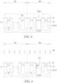
- FIG. 1 to FIG. 10 are schematic cross-sectional views of a process for fabricating a semiconductor structure according to a preferred embodiment of the present invention.
- FIG. 1 to FIG. 10 are schematic cross-sectional views of a process for fabricating a semiconductor structure according to a preferred embodiment of the present invention.
- a substrate 10 such as a silicon substrate
- a first region R 1 and a second region R 2 are defined on the substrate 10 , in which different transistors will be formed in the first region R 1 and the second region R 2 in subsequent steps.
- transistors with different oxide thicknesses can be formed in the two regions respectively, especially when these transistors are applied with larger and different voltages (i.e., these transistors are high-voltage devices), in order to prevent the current passing through the transistors from being affected, different transistors need to have oxide layers matching the voltage.
- One of the purposes of this embodiment is to fabricate transistors with different oxide thicknesses on the same substrate, so as to allow different voltages to be applied to different transistors, thereby increasing the application range of products.
- a well region 11 and a doped region 12 are formed in the substrate 10 by doping.
- the well region 11 and the doped region 12 have different doping concentrations, and the doped region 12 can be used as a source/drain region of a transistor which is formed in the subsequent steps.
- a plurality of shallow trench isolations 14 are formed in the doped regions 12 .
- the material of the shallow trench isolations 14 is, for example, silicon oxide.
- One part of the shallow trench isolations 14 is located in the doped regions 12 of the substrate 10 (i.e., into the substrate 10 ), and the other part protrudes from the surface of the substrate 10 .
- a thin oxide layer 15 may be formed on the surface of the substrate 10 between the shallow trench isolation 14 .
- a mask layer 16 is formed to cover the substrate 10 and each shallow trench isolation 14 .
- the material of the mask layer 16 is, but not limited to, silicon nitride.
- a patterned photoresist layer 18 is formed over the mask layer 16 , the patterned photoresist layer 18 includes an opening OP 1 exposing a part of the region where the gate structure of the transistor is to be formed later. For example, the region disposed just above the well region 11 between two doped regions 12 in the first region R 1 .
- an etching step P 1 is performed to remove part of the mask layer 16 and the underlying substrate (including part of the well region 11 and part of the doped region 12 ) using the patterned photoresist layer 18 as a mask, so as to form a first groove G 1 in the first region R 1 .
- the first groove G 1 has a first depth D 1 .
- the patterned photoresist layer 18 is removed.
- the patterned photoresist layer 20 includes an opening OP 2 formed in the second region R 2 , and the opening OP 12 exposes a part of the region where the gate structure of the transistor is to be formed later, for example, the region disposed just above the well region 11 between two doped regions 12 in the second region R 2 .
- an etching step P 2 is performed, and using the patterned photoresist layer 20 as a mask to remove part of the mask layer 16 and the underlying substrate (including part of the well region 11 and part of the doped region 12 ), so as to form a second groove G 2 in the second region R 2 .
- the second groove G 2 has a second depth D 2 which is different from the first depth D 1 .
- the second depth D 2 is greater than the first depth D 1 .
- an oxidation step P 3 is performed to form an oxide layer 22 A and an oxide layer 22 B in the first groove G 1 and the second groove G 2 respectively. Since the oxidation rates are nearly equal in the two grooves, and the second groove G 2 is deeper than the first groove G 1 , so the top surface height of the oxide layer 22 B in the second groove G 2 is lower than that of the oxide layer 22 A in the first groove G 1 after the oxide layers 22 A and the oxide layer 22 B are completed. Thereafter, the mask layer 16 is removed to expose the thin oxide layer 15 on the surface of the substrate 10 .
- another oxidation step (not shown) can be used to increase the thickness of the thin oxide layer 15 , or another oxide layer can be re-formed after removing the thin oxide layer 15 , which can be used as the gate dielectric layer of other gate devices (not for the high voltage transistors).
- the oxide layer 22 A in the first groove G 1 is higher than the oxide layer 22 B in the second groove G 2 , that is, there is a height difference H 1 between them.
- another patterned photoresist layer 24 is formed to cover the substrate 10 , and the patterned photoresist layer 24 has an opening OP 3 exposing the oxide layer 22 A in the first groove G 1 .
- the width of the opening OP 3 here can also be same as the width of the gate structure which is formed in later steps, so as to save the number of masks.
- an etching-back step P 4 is performed to remove part of the oxide layer 22 A.
- the etching parameters can be controlled to adjust the top surfaces of the oxide layers 22 A and 22 B in the first groove G 1 and the second groove G 2 to be nearly horizontally aligned with each other. That is, the original height difference H 1 between the oxide layers 22 A and 22 B has been nearly eliminated.
- the top surface of the shallow trench isolation 14 and the top surface of the oxide layer 22 A or 22 B still have a height difference H 2 , which will affect the formation of the subsequent gate structure.
- another patterned photoresist layer 26 is formed to cover the regions on the oxide layers 22 A and 22 B.
- the patterned photoresist layer 26 can correspond to the positions of the oxide layers 22 A and 22 B, and the shallow trench isolation 14 is not covered by the patterned photoresist layer 26 , so as to protect the oxide layers 22 A and 22 B from being damaged in the next etching step.
- the patterned photoresist layer 26 here can also correspond to the patterns of other gate structures (such as non-high voltage gate structures located in other regions). That is to say, except for eliminating the height difference H 2 , the positions of the gate structures in other regions can also be defined. Then, as shown in FIG.
- the thin oxide layer 15 uncovered by the patterned photoresist layer 26 and part of the shallow trench isolation 14 are removed by an etching-back step P 5 .
- the top surfaces of the oxide layers 22 A and 22 B are flush with the top surface of the substrate 10 .
- the steps shown in FIG. 6 to FIG. 9 above using the patterned photoresist layer as a protective layer, the protruding portion of the oxide layer 22 A and part of the shallow trench isolation 14 and the thin oxide layer 15 are removed, so that the top surfaces of the oxide layers 22 A and 22 B are flush with the substrate 10 .
- planarization e.g., chemical mechanical polishing
- the steps shown in FIG. 6 to FIG. 9 can more accurately remove part of the oxide layer 22 A, so that the top surfaces of the substrate 10 and the oxide layers 22 A and 22 B are flatter, which is beneficial to the subsequent formation of the gate structure.
- gate structures 28 A and 28 B are respectively formed on the oxide layer 22 A and the oxide layer 22 B.
- the gate structures 28 A and 28 B are, for example, polysilicon gates, which are used as the gates of a high voltage transistor.
- gate structures 28 A and 28 B are located directly above the oxide layer 22 A and the oxide layer 22 B respectively.
- Other devices e.g., contact structures to connect with gate structures may be formed later, and the formation methods of these devices belong to the conventional technology in the field, so they will not be described in detail here.
- the invention is characterized in that grooves with different depths are formed on the same substrate, and then oxidation steps are carried out in the grooves to form oxide layers 22 A and 22 B with different thicknesses as oxide layers of different high voltage transistors.
- high voltage transistors with different oxide layer thicknesses can be formed on the same substrate, so that the method can be applied to various products.
- the operating voltage of thin film transistors made of low temperature polysilicon (LTPS) is about 20V
- the operating voltage of thin film transistors made of low temperature polysilicon oxide (LTPO) is about 27V
- the two transistors have suitable oxide layer thicknesses.
- the present invention provides a method for fabricating two transistors with different operating voltages on the same substrate, so that the flexibility of the manufacturing process can be improved, for example, more diversified circuit structures can be combined.
- the method provided by the invention can be compatible with the existing process, and transistors with different thicknesses of oxide layers can be manufactured without spending a lot of cost.
- the steps of the invention are repeated many times, more kinds of oxide layers with different thicknesses can be produced. This feature is also within the scope of the present invention.
- the present invention provides a method for forming a semiconductor structure, which comprises providing a substrate 10 , sequentially forming a first groove G 1 and a second groove G 2 in the substrate 10 , the depth D 1 of the first groove G 1 is different from the depth D 2 of the second groove G 2 , a first oxide layer 22 A is formed in the first groove G 1 and a second oxide layer 22 B is formed in the second groove G 2 , and an etching step P 4 is performed to remove part of the first oxide layer 22 A, and a first gate structure 28 A is formed on the first oxide layer 22 A and a second gate structure 28 B is formed on the second oxide layer 22 B.
- the height of the first oxide layer 22 A is different from that of the second oxide layer 22 B.
- the first oxide layer 22 A and the second oxide layer 22 B are simultaneously formed in the first groove G 1 and the second groove G 2 respectively by an oxidation step P 3 .
- the top surfaces of the first oxide layer 22 A and the second oxide layer 22 B have the same height.
- the first oxide layer 22 A and the first gate junction 28 A constitute a first high voltage transistor
- the second oxide layer 22 B and the second gate structure 28 B constitute a second high voltage transistor, different voltages are applied to the first high voltage transistor and the second high voltage transistor.
- the first oxide layer 22 A is the gate oxide layer in the first high voltage transistor
- the second oxide layer 22 B is the gate oxide layer in the second high voltage transistor.
- the etching-back step P 4 includes multiple etch-back steps, and one of the etch-back steps includes forming a patterned photoresist layer 24 covering the substrate 10 , the patterned photoresist layer 24 including an opening OP 3 exposing part of the first oxide layer 22 A, and removing part of the first oxide layer 22 A and reducing the height of the first oxide layer 22 A by an etching-back step P 4 .
- the width of the opening OP 3 of the patterned photoresist layer 24 is the same as the width of the first gate structure 28 A.
- Some embodiments of the present invention further include forming a plurality of shallow trench isolations 14 in the substrate 10 , the first oxide layer is located between two shallow trench isolations and connected with two adjacent shallow trench isolations.
- the depth of the shallow trench isolation 14 is greater than the depth of the first oxide layer 22 A.
- the invention provides a semiconductor structure, which comprises a substrate 10 , a first oxide layer 22 A and a second oxide layer 22 B in the substrate 10 , wherein the first oxide layer 22 A and the second oxide layer 22 B have different thicknesses, and a first gate structure 28 A on the first oxide layer 22 A and a second gate structure 28 B on the second oxide layer 22 B.
- the first oxide layer 22 A and the second oxide layer 22 B are not connected with each other.
- Some embodiments of the present invention further include a plurality of shallow trench isolations 14 located in the substrate 10 , the first oxide layer 22 A is located between two shallow trench isolations 14 and connected with two adjacent shallow trench isolations 14 .
- the depth of the shallow trench isolation 14 is greater than the depth of the first oxide layer 22 A.
- the top surface of the first oxide layer 22 A is flush with the top surface of the second oxide layer 22 B, but the bottom surface of the first oxide layer 22 A and the bottom surface of the second oxide layer 22 B are located at different levels.
- the first oxide layer 22 A and the first gate structure 28 A constitute a first high voltage transistor
- the second oxide layer 22 B and the second gate structure 28 B constitute a second high voltage transistor
- the invention is characterized in that grooves with different depths are formed on the same substrate, and then the grooves with different depths are respectively made into oxide layers of high voltage transistors.
- high voltage transistors with oxide layers of different thicknesses can be formed on the same substrate.
- the thickness of the oxide layer can be adjusted according to the operating voltage of each high voltage transistor, so that the problem of performance reduction caused by mismatch between the operating voltage and the thickness of the oxide layer can be avoided.
- many different high voltage transistors are fabricated on the same substrate at the same time, which can also increase the flexibility of the manufacturing process.
- the method provided by the invention is compatible with the existing manufacturing process and does not need to spend a lot of extra cost.
Landscapes
- Element Separation (AREA)
- Insulated Gate Type Field-Effect Transistor (AREA)
- Metal-Oxide And Bipolar Metal-Oxide Semiconductor Integrated Circuits (AREA)
Abstract
Description
Claims (14)
Applications Claiming Priority (2)
| Application Number | Priority Date | Filing Date | Title |
|---|---|---|---|
| TW110133685A TWI880026B (en) | 2021-09-10 | 2021-09-10 | Semiconductor structure and forming method thereof |
| TW110133685 | 2021-09-10 |
Publications (2)
| Publication Number | Publication Date |
|---|---|
| US20230080968A1 US20230080968A1 (en) | 2023-03-16 |
| US12046596B2 true US12046596B2 (en) | 2024-07-23 |
Family
ID=85479215
Family Applications (1)
| Application Number | Title | Priority Date | Filing Date |
|---|---|---|---|
| US17/495,783 Active 2042-12-09 US12046596B2 (en) | 2021-09-10 | 2021-10-06 | Semiconductor structure and forming method thereof |
Country Status (2)
| Country | Link |
|---|---|
| US (1) | US12046596B2 (en) |
| TW (1) | TWI880026B (en) |
Citations (10)
| Publication number | Priority date | Publication date | Assignee | Title |
|---|---|---|---|---|
| US20070210403A1 (en) * | 2006-03-07 | 2007-09-13 | Micron Technology, Inc. | Isolation regions and their formation |
| US20110057287A1 (en) * | 2004-08-12 | 2011-03-10 | Renesas Electronics Corporation | Semiconductor device having dual-sti and manufacturing method thereof |
| US20120074498A1 (en) * | 2010-09-27 | 2012-03-29 | Taiwan Semiconductor Manufacturing Company, Ltd. | Method and apparatus for improving gate contact |
| US20130062682A1 (en) * | 2011-09-14 | 2013-03-14 | Masato Endo | Semiconductor memory and manufacturing method thereof |
| US20130241027A1 (en) * | 2012-03-19 | 2013-09-19 | Samsung Electronics Co., Ltd. | Semiconductor device having isolation region |
| US9825146B2 (en) * | 2012-07-17 | 2017-11-21 | SK Hynix Inc. | Dummy bit line MOS capacitor and device using the same |
| US10411088B2 (en) | 2016-10-06 | 2019-09-10 | United Microelectronics Corp. | Semiconductor device |
| US20200203215A1 (en) * | 2018-12-24 | 2020-06-25 | Samsung Electronics Co., Ltd. | Semiconductor devices |
| US20200381292A1 (en) * | 2019-05-31 | 2020-12-03 | Samsung Electronics Co., Ltd. | Semiconductor device including trench isolation layer and method of forming the same |
| US20210126098A1 (en) * | 2019-10-24 | 2021-04-29 | Samsung Electronics Co., Ltd. | Semiconductor device |
Family Cites Families (1)
| Publication number | Priority date | Publication date | Assignee | Title |
|---|---|---|---|---|
| DE102017125541B4 (en) * | 2017-06-30 | 2020-02-27 | Taiwan Semiconductor Manufacturing Co., Ltd. | Semiconductor device with memory cell area and circuit areas, and method for their production |
-
2021
- 2021-09-10 TW TW110133685A patent/TWI880026B/en active
- 2021-10-06 US US17/495,783 patent/US12046596B2/en active Active
Patent Citations (10)
| Publication number | Priority date | Publication date | Assignee | Title |
|---|---|---|---|---|
| US20110057287A1 (en) * | 2004-08-12 | 2011-03-10 | Renesas Electronics Corporation | Semiconductor device having dual-sti and manufacturing method thereof |
| US20070210403A1 (en) * | 2006-03-07 | 2007-09-13 | Micron Technology, Inc. | Isolation regions and their formation |
| US20120074498A1 (en) * | 2010-09-27 | 2012-03-29 | Taiwan Semiconductor Manufacturing Company, Ltd. | Method and apparatus for improving gate contact |
| US20130062682A1 (en) * | 2011-09-14 | 2013-03-14 | Masato Endo | Semiconductor memory and manufacturing method thereof |
| US20130241027A1 (en) * | 2012-03-19 | 2013-09-19 | Samsung Electronics Co., Ltd. | Semiconductor device having isolation region |
| US9825146B2 (en) * | 2012-07-17 | 2017-11-21 | SK Hynix Inc. | Dummy bit line MOS capacitor and device using the same |
| US10411088B2 (en) | 2016-10-06 | 2019-09-10 | United Microelectronics Corp. | Semiconductor device |
| US20200203215A1 (en) * | 2018-12-24 | 2020-06-25 | Samsung Electronics Co., Ltd. | Semiconductor devices |
| US20200381292A1 (en) * | 2019-05-31 | 2020-12-03 | Samsung Electronics Co., Ltd. | Semiconductor device including trench isolation layer and method of forming the same |
| US20210126098A1 (en) * | 2019-10-24 | 2021-04-29 | Samsung Electronics Co., Ltd. | Semiconductor device |
Also Published As
| Publication number | Publication date |
|---|---|
| TW202312247A (en) | 2023-03-16 |
| US20230080968A1 (en) | 2023-03-16 |
| TWI880026B (en) | 2025-04-11 |
Similar Documents
| Publication | Publication Date | Title |
|---|---|---|
| US10290718B2 (en) | Metal-oxide-semiconductor transistor and method of forming gate layout | |
| US7385274B2 (en) | High-voltage metal-oxide-semiconductor devices and method of making the same | |
| US9660022B2 (en) | Semiconductive device with a single diffusion break and method of fabricating the same | |
| US20070158780A1 (en) | Semiconductor integrated circuit device and method of fabricating the same | |
| TWI783064B (en) | Semiconductor device and method of forming the same | |
| TWI533408B (en) | Thin film transistor and active matrix organic light emitting diode assembly and manufacturing method thereof | |
| KR20130100660A (en) | Semiconductor devices and manufacturing and design methods thereof | |
| TWI701763B (en) | Transistor structure and semiconductor layout structure | |
| US8049283B2 (en) | Semiconductor device with deep trench structure | |
| US20070278613A1 (en) | Semiconductor device | |
| US11121042B2 (en) | Production of semiconductor regions in an electronic chip | |
| US7485925B2 (en) | High voltage metal oxide semiconductor transistor and fabricating method thereof | |
| US20130037882A1 (en) | Semiconductor device | |
| US20250194178A1 (en) | Method for forming a semiconductor high-voltage device having a buried gate dielectric layer | |
| US9324786B2 (en) | Semiconductor device and method for fabricating the same | |
| US12046596B2 (en) | Semiconductor structure and forming method thereof | |
| US12224335B2 (en) | Semiconductor device and fabrication method thereof | |
| CN114765171B (en) | Semiconductor structure and manufacturing method thereof | |
| KR101006519B1 (en) | Semiconductor device and manufacturing method thereof | |
| TWI866737B (en) | Semiconductor process | |
| US20200144101A1 (en) | Semiconductor structures and fabrication method thereof | |
| US11735657B2 (en) | Method for fabricating transistor structure | |
| TW202545329A (en) | Semiconductor device and method for fabricating the same | |
| CN119562558A (en) | Medium voltage transistor structure and manufacturing method thereof | |
| KR100679833B1 (en) | Semiconductor device and manufacturing method thereof |
Legal Events
| Date | Code | Title | Description |
|---|---|---|---|
| AS | Assignment |
Owner name: UNITED MICROELECTRONICS CORP., TAIWAN Free format text: ASSIGNMENT OF ASSIGNORS INTEREST;ASSIGNORS:HUANG, WEI-LUN;WANG, CHIA-LING;LU, CHIA-WEN;AND OTHERS;REEL/FRAME:057722/0052 Effective date: 20210930 |
|
| FEPP | Fee payment procedure |
Free format text: ENTITY STATUS SET TO UNDISCOUNTED (ORIGINAL EVENT CODE: BIG.); ENTITY STATUS OF PATENT OWNER: LARGE ENTITY |
|
| STPP | Information on status: patent application and granting procedure in general |
Free format text: DOCKETED NEW CASE - READY FOR EXAMINATION |
|
| STPP | Information on status: patent application and granting procedure in general |
Free format text: NON FINAL ACTION MAILED |
|
| STPP | Information on status: patent application and granting procedure in general |
Free format text: RESPONSE TO NON-FINAL OFFICE ACTION ENTERED AND FORWARDED TO EXAMINER |
|
| STPP | Information on status: patent application and granting procedure in general |
Free format text: AWAITING TC RESP., ISSUE FEE NOT PAID |
|
| STPP | Information on status: patent application and granting procedure in general |
Free format text: NOTICE OF ALLOWANCE MAILED -- APPLICATION RECEIVED IN OFFICE OF PUBLICATIONS |
|
| STPP | Information on status: patent application and granting procedure in general |
Free format text: PUBLICATIONS -- ISSUE FEE PAYMENT VERIFIED |
|
| STCF | Information on status: patent grant |
Free format text: PATENTED CASE |