US12029034B2 - Semiconductor storage device and manufacturing method thereof - Google Patents
Semiconductor storage device and manufacturing method thereof Download PDFInfo
- Publication number
- US12029034B2 US12029034B2 US17/006,656 US202017006656A US12029034B2 US 12029034 B2 US12029034 B2 US 12029034B2 US 202017006656 A US202017006656 A US 202017006656A US 12029034 B2 US12029034 B2 US 12029034B2
- Authority
- US
- United States
- Prior art keywords
- layers
- columnar
- insulating
- storage device
- semiconductor storage
- Prior art date
- Legal status (The legal status is an assumption and is not a legal conclusion. Google has not performed a legal analysis and makes no representation as to the accuracy of the status listed.)
- Active, expires
Links
Images


Classifications
-
- H—ELECTRICITY
- H01—ELECTRIC ELEMENTS
- H01L—SEMICONDUCTOR DEVICES NOT COVERED BY CLASS H10
- H01L23/00—Details of semiconductor or other solid state devices
- H01L23/48—Arrangements for conducting electric current to or from the solid state body in operation, e.g. leads, terminal arrangements ; Selection of materials therefor
- H01L23/481—Internal lead connections, e.g. via connections, feedthrough structures
-
- H—ELECTRICITY
- H10—SEMICONDUCTOR DEVICES; ELECTRIC SOLID-STATE DEVICES NOT OTHERWISE PROVIDED FOR
- H10B—ELECTRONIC MEMORY DEVICES
- H10B43/00—EEPROM devices comprising charge-trapping gate insulators
- H10B43/20—EEPROM devices comprising charge-trapping gate insulators characterised by three-dimensional arrangements, e.g. with cells on different height levels
- H10B43/23—EEPROM devices comprising charge-trapping gate insulators characterised by three-dimensional arrangements, e.g. with cells on different height levels with source and drain on different levels, e.g. with sloping channels
- H10B43/27—EEPROM devices comprising charge-trapping gate insulators characterised by three-dimensional arrangements, e.g. with cells on different height levels with source and drain on different levels, e.g. with sloping channels the channels comprising vertical portions, e.g. U-shaped channels
-
- H—ELECTRICITY
- H10—SEMICONDUCTOR DEVICES; ELECTRIC SOLID-STATE DEVICES NOT OTHERWISE PROVIDED FOR
- H10B—ELECTRONIC MEMORY DEVICES
- H10B43/00—EEPROM devices comprising charge-trapping gate insulators
- H10B43/30—EEPROM devices comprising charge-trapping gate insulators characterised by the memory core region
- H10B43/35—EEPROM devices comprising charge-trapping gate insulators characterised by the memory core region with cell select transistors, e.g. NAND
-
- H—ELECTRICITY
- H10—SEMICONDUCTOR DEVICES; ELECTRIC SOLID-STATE DEVICES NOT OTHERWISE PROVIDED FOR
- H10B—ELECTRONIC MEMORY DEVICES
- H10B43/00—EEPROM devices comprising charge-trapping gate insulators
- H10B43/40—EEPROM devices comprising charge-trapping gate insulators characterised by the peripheral circuit region
-
- H10W20/20—
Definitions
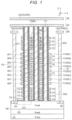
- FIG. 1 is a diagram illustrating a memory cell array in a semiconductor storage device according to a first embodiment.
- FIGS. 2 A and 2 B are schematic cross-sectional views illustrating a memory cell in a three-dimensional structure.
- FIG. 3 is a schematic plan view illustrating a memory cell array.
- FIG. 4 is a cross-sectional view taken along a line 4-4 of FIG. 3 .
- FIG. 13 is a schematic plan view illustrating an example of an arrangement of columnar portions and contact plugs in the stacked body according to a third embodiment.
- FIG. 14 is a cross-sectional view illustrating an example of a stacked body in a lead area of a memory cell array of a semiconductor storage device according to a fourth embodiment.
- FIGS. 15 - 20 are cross-sectional views illustrating aspects of a method of manufacturing a semiconductor storage device according to a fourth embodiment.
- FIG. 21 is a cross-sectional view illustrating an example of a stacked body in a lead area of a memory cell array of a semiconductor storage device according to a modified embodiment.
- a semiconductor storage device and a manufacturing method of a semiconductor storage device for which deformation of the stacked structure in the semiconductor storage device can be prevented are described.
- a semiconductor storage device includes a stacked body, a first columnar portion, a second columnar portion, and second insulating layers.
- the stacked body includes a plurality of conductive layers and a plurality of first insulating layers alternately stacked in a first direction. A first area and a second area adjacent to each other are in the stacked body.
- the first columnar portion is provided in the first area, penetrates the stacked body in the first direction and includes a semiconductor layer.
- the second columnar portion is provided in the second area and penetrates the stacked body in the first direction.
- the second insulating layers are provided between the second columnar portion and either the conductive layers or the first insulating layers, depending on embodiment.
- a third insulating layer is on the second columnar portion such that the second insulating layers are between the third insulating layer and the conductive layers or the first insulating layers, depending on the particular embodiment.
- the vertical direction of a semiconductor substrate is a relative direction in which the surface on which the semiconductor element is provided is up and may be different from the vertical direction according to the gravitational acceleration.
- the drawings are schematic or conceptual, and the proportions of the respective parts are not necessarily the same as the actual ones.
- elements similar to those described in regard to the drawings already described are denoted by the same reference numerals, and detailed description thereof is appropriately omitted.
- FIG. 1 is a diagram illustrating an example of a configuration of a memory cell array in a semiconductor storage device according to a first embodiment.
- a memory cell array MCA (see FIG. 3 ) is, for example, a memory cell array in which memory cells are three dimensionally arranged (also referred to as a “3D memory cell array” or the like).
- the insulating portions other than an insulating film formed in memory holes 113 are not illustrated in FIG. 1 .
- silicon is exemplified as a semiconductor material, but a semiconductor other than silicon may be used in other examples.
- an XYZ orthogonal coordinate system is introduced.
- two directions parallel to the main surface of a substrate 100 and orthogonal to each other are defined as an X direction and a Y direction, and a direction orthogonal to both the X direction and the Y direction is defined as a Z direction.
- a plurality of word lines (conductive layers) WL are stacked in the Z direction.
- an n type well region 101 is formed on the semiconductor substrate 100 , and a p type well region 102 is formed on the n type well region 101 .
- a plurality of NAND strings NS are formed on the p type well region 102 .
- a plurality of interconnection layers 110 functioning as select gate lines SGS, a plurality of interconnection layers 111 functioning as word lines WL, and a plurality of interconnection layers 112 functioning as select gate lines SGD are formed on the p type well region 102 .
- interconnection layers 110 are formed, electrically connected to the common select gate line SGS via the plurality of NAND strings NS, and function as gate electrodes of two select transistors ST2.
- each layer is electrically connected to the common word line WL.
- interconnection layers 112 are formed, are electrically connected to the select gate line SGD corresponding to each of the NAND string NS, and each layer functions as a gate electrode of one select transistor ST1.
- the memory hole 113 penetrates the interconnection layers 110 , 111 , and 112 and reaches the p type well region 102 .
- a block insulating film 114 , a charge storage layer 115 (insulating film), and a gate insulating film 116 are sequentially formed on the side surface of the memory hole 113 .
- Conductive films 117 are embedded in the memory hole 113 .
- the conductive films 117 function as current paths of the NAND strings NS.
- An interconnection layer 118 functioning as a bit line BL is formed on upper ends of the conductive films 117 . Further details of the memory hole 113 are described below with reference to FIGS. 2 A and 2 B .
- the select transistors ST2, a plurality of memory cell transistors MT, and the select transistor ST1 are sequentially stacked on the p type well region 102 , and one memory hole 113 corresponds to one NAND string NS.
- a contact plug 121 is formed on the p+ type impurity diffusion layer 104 , and an interconnection layer 122 functioning as a well wiring CPWELL is formed on the contact plug 121 .
- M0 layers in which the interconnection layers 120 and 122 are formed are formed over the interconnection layers 112 (the select gate lines SGD) and under an M1 layer on which the interconnection layer 118 is formed.
- a plurality of the above configurations are arranged in a depth direction of FIG. 1 (that is, in the direction into the page of FIG. 1 ).
- One branch is configured with a set of the plurality of NAND strings NS arranged along a line in the depth direction.
- the interconnection layers 110 function as the common select gate line SGS in the same block and are electrically connected to each other.
- the gate insulating film 116 at its lower end extends between the lowermost interconnection layer 110 and the upper surface of the p type well region 102 .
- Both the lowermost interconnection layer 110 which is adjacent to the n+ type impurity diffusion layer 103 , and the lower end portion of the gate insulating film 116 , which extends underneath that lowermost interconnection layer 110 , are formed further extending to the vicinity of the n+ type impurity diffusion layer 103 .
- the thus-formed channel electrically connects the memory cell transistor MT0 and the n+ type impurity diffusion layer 103 .
- the voltage generation circuit can give a potential to the conductive films 117 by applying a voltage to the well wiring CPWELL.
- FIGS. 2 A and 2 B are schematic cross-sectional views illustrating a memory cell in a three-dimensional structure.
- a plurality of pillars CL are provided in the memory hole 113 (hereinafter, also referred to as a memory hole MH).
- Each of the plurality of pillars CL includes a semiconductor body 210 , a memory film 220 , and a core layer 230 .
- Block insulating films 21 a that constitute a portion of the memory film 220 may be provided between conductive layers 21 (which ultimately function as word lines WL in the present embodiment) and insulating layers 22 .
- the block insulating film 21 a is, for example, a silicon oxide film or a metal oxide film.
- metal oxide is aluminum oxide.
- Barrier films 21 b may be provided between the conductive layers 21 and the insulating layers 22 and between the conductive layers 21 and the memory film 220 .
- each of the conductive layer 21 is, for example, tungsten
- a stacked structure film of titanium nitride and titanium is selected as the barrier film 21 b .
- the block insulating film 21 a prevent back tunneling of charges from the conductive layer 21 to the memory film 220 side.
- the barrier film 21 b improves adhesion between the conductive layer 21 and the block insulating film 21 a.
- the memory film 220 is provided between the inner surface of the memory hole MH and the semiconductor body 210 .
- the shape of the memory film 220 is, for example, a cylindrical shape.
- Each of the memory cells MC has a storage region between the semiconductor body 210 and the conductive layer 21 to be the word line WL. These memory cells MC are stacked in the Z axis direction.
- the memory film 220 includes, for example, a cover insulating film 221 , a charge trapping film 222 , and a tunnel insulating film 223 .
- Each of the semiconductor body 210 , the charge trapping film 222 , and the tunnel insulating film 223 extends in the Z axis direction.
- the cover insulating film 221 is between the conductive layers 21 and the charge trapping film 222 and also between the insulating layers 22 and the charge trapping film 222 .
- the cover insulating film 221 includes, for example, silicon oxide.
- the cover insulating film 221 protects the charge trapping film 222 so as not to be etched when a sacrificial film is replaced with the conductive layer 21 in a replacing step.
- the cover insulating film 221 may be removed from a portion between the conductive layer 21 and the memory film 220 .
- the block insulating film 21 a is provided between the conductive layer 21 and the charge trapping film 222 .
- the cover insulating film 221 may not be used.
- the charge trapping film 222 is provided between the cover insulating film 221 and the tunnel insulating film 223 .
- the charge trapping film 222 includes, for example, silicon nitride and has a trap site for trapping charges in the film.
- a portion interposed between the conductive layers 21 (which function as the word lines WL) and the semiconductor body 210 constitutes the storage region of the memory cell MC as a charge trapping portion.
- the threshold voltage of the memory cell MC changes depending on whether there is a charge in the charge trapping portion or the amount of the charges trapped in the charge trapping portion. Accordingly, the memory cell MC stores information.
- the tunnel insulating film 223 is provided between the semiconductor body 210 and the charge trapping film 222 .
- the tunnel insulating film 223 includes, for example, silicon oxide or silicon oxide and silicon nitride.
- the tunnel insulating film 223 is a potential barrier between the semiconductor body 210 and the charge trapping film 222 .
- the electrons and the holes each pass through (tunnel) the potential barrier of the tunnel insulating film 223 .
- FIG. 3 is a schematic plan view illustrating an example of the configuration of the memory cell array MCA.
- the memory cell array MCA has a stacked structure of the conductive layers 21 and the insulating layers 22 and has a plurality of memory cells arranged three dimensionally.
- the conductive layer 21 is referred to as a conductive layer WL
- the insulating layer 22 is referred to as an insulating layer 25 .
- FIG. 4 is a cross-sectional view taken along a line 4-4 of FIG. 3 .
- FIG. 4 also illustrates the contact plugs 40 seen in the direction of the cross section with dotted lines.
- the stacked body 200 includes the plurality of conductive layers WL and the plurality of insulating layers 25 (may also be referred to as “first insulating layers” herein) which are alternately stacked in the stacking direction (may also be referred to as “first direction” herein).
- the cell area AR1 and the lead area AR2 seen in the stacking direction are defined in the stacked body 200 . That is, the stacked body 200 includes the cell area AR1 and the lead area AR2.
- a conductive material such as tungsten or doped silicon is used for the conductive layer WL.
- an insulating material such as a silicon oxide film is used for the insulating layer 25 .
- the plurality of pillars CL are provided in the cell area AR1 to penetrate the stacked body 200 in the stacking direction.
- Each pillar CL includes a semiconductor layer.
- the columnar portions CLHR are provided in the lead area AR2 to penetrate the stacked body 200 in the stacking direction.
- sacrificial layers that are sandwiched between the insulting layers 25 in the stacked body 200 , will be removed to create gaps or cavities (hereinafter, collectively referred to as “gaps”) where the conductive layers WL will subsequently be formed, and due to the gaps prior to the formation of the conductive layers WL, the insulating layers 25 may bend or deform.
- the diameter of each of the columnar portions CLHR decreases downward in the stacking direction of the stacked body 200 .
- a plurality of holes HR may be formed in the stacked body 200 by the reactive ion etching (RIE) method, which makes the diameter of each of the hole HR gradually decrease in the thickness direction of the stacked body 200 , and the columnar portion CLHR to be formed in each hole HR will have its diameter decrease in the same manner.
- RIE reactive ion etching
- Each columnar portion CLHR includes one or more insulating layers (which may also be referred to as “third insulating layers” herein).
- the insulating layers prevent electrical conduction between the conductive layers WL via the columnar portion CLHR.
- Each columnar portion CLHR may be filled with, for example, an insulating material such as silicon oxide (SiO 2 ).
- an insulating material such as silicon oxide (SiO 2 ).
- the present embodiment is not limited to this, and other ways are available, taking into consideration the strength of the columnar portion CLHR.
- silicon nitride (SiN) and the like may be used, or a structure in which an insulating spacer of silicon oxide or the like is provided around metal or silicon nitride may be used.
- the columnar portion CLHR is electrically insulated from the conductive layer WL by the insulating spacer.
- the insulating layer included in the columnar portion CLHR is provided at least on the side surface of the columnar portion CLHR.
- the insulating layers SP1 are between the insulating layer of the columnar portion CLHR and the conductive layers WL or the insulating layers 25 .
- the insulating layers SP1 are provided between the conductive layers WL and the one or more insulating layers of the columnar portions CLHR.
- the insulating layers SP1 are provided on the outer periphery of each of the columnar portions CLHR in the plane parallel to the conductive layers WL.
- the plurality of insulating layers SP1 extend annularly from the outer periphery of each columnar portion CLHR. This makes the diameter of each columnar portion CLHR in the plane parallel to the conductive layers WL, that is the total diameter of the columnar portion CLHR and insulating layer SP1 in the same plane, increase.
- FIG. 4 the insulating layers SP1 are provided between the conductive layers WL and the one or more insulating layers of the columnar portions CLHR.
- the insulating layers SP1 are provided on the outer periphery of each of the columnar portions CLHR in the plane parallel to the conductive layers WL.
- the plurality of insulating layers SP1 extend annularly from the outer periphery of each
- the region of each of the conductive layers WL decreases because of the insulating layer SP1 in the same plane. Accordingly, prior to or during the process of forming the conductive layers WL in the gaps created by the removal of the sacrificial layers between the stacked insulating layers 25 , the insulating layers SP1 can support the insulating layers 25 together with the columnar portions CLHR and further narrow the regions of the gaps. Accordingly, possible deformation, such as bending, of the insulating layers 25 due to the gaps can be further effectively prevented. As a result, possible deformation of the stacked structure 200 due to such deformation of the insulating layers 25 is also effectively prevented, and the reliability of the semiconductor storage device comprising the stacked structure 200 can be improved or maintained at a desired level.
- the insulating layers SP1 are provided below a predetermined position P as shown in FIG. 4 .
- the position P is determined as a position where the diameter of the columnar portion CLHR becomes small to a certain extent as it stretches downward in the stacking direction in the staked body 200 , and the insulating layers SP1 are provided below such position in part of the columnar portion CLHR having the small diameter.
- an insulating material such as silicon oxide is used, for example.
- FIGS. 5 to 11 are cross-sectional view illustrating an example of a method of manufacturing the semiconductor storage device according to the first embodiment.
Landscapes
- Semiconductor Memories (AREA)
- Non-Volatile Memory (AREA)
- Physics & Mathematics (AREA)
- Condensed Matter Physics & Semiconductors (AREA)
- General Physics & Mathematics (AREA)
- Engineering & Computer Science (AREA)
- Computer Hardware Design (AREA)
- Microelectronics & Electronic Packaging (AREA)
- Power Engineering (AREA)
- Internal Circuitry In Semiconductor Integrated Circuit Devices (AREA)
Abstract
Description
Claims (14)
Applications Claiming Priority (2)
| Application Number | Priority Date | Filing Date | Title |
|---|---|---|---|
| JP2020029627A JP2021136270A (en) | 2020-02-25 | 2020-02-25 | Semiconductor storage device and method for manufacturing the same |
| JP2020-029627 | 2020-02-25 |
Publications (2)
| Publication Number | Publication Date |
|---|---|
| US20210265386A1 US20210265386A1 (en) | 2021-08-26 |
| US12029034B2 true US12029034B2 (en) | 2024-07-02 |
Family
ID=77366436
Family Applications (1)
| Application Number | Title | Priority Date | Filing Date |
|---|---|---|---|
| US17/006,656 Active 2041-01-06 US12029034B2 (en) | 2020-02-25 | 2020-08-28 | Semiconductor storage device and manufacturing method thereof |
Country Status (4)
| Country | Link |
|---|---|
| US (1) | US12029034B2 (en) |
| JP (1) | JP2021136270A (en) |
| CN (1) | CN113380818B (en) |
| TW (1) | TWI746072B (en) |
Families Citing this family (2)
| Publication number | Priority date | Publication date | Assignee | Title |
|---|---|---|---|---|
| JP2023090170A (en) * | 2021-12-17 | 2023-06-29 | キオクシア株式会社 | semiconductor storage device |
| JP2026004726A (en) * | 2024-06-26 | 2026-01-15 | 東京エレクトロン株式会社 | Film forming method and film forming apparatus |
Citations (28)
| Publication number | Priority date | Publication date | Assignee | Title |
|---|---|---|---|---|
| US20040043550A1 (en) | 2002-07-31 | 2004-03-04 | Hiraku Chakihara | Semiconductor memory device and a method of manufacturing the same, a method of manufacturing a vertical MISFET and a vertical MISFET, and a method of manufacturing a semiconductor device and a semiconductor device |
| US20100163968A1 (en) * | 2008-12-31 | 2010-07-01 | Samsung Electronics Co., Ltd. | Semiconductor memory device having insulation patterns and cell gate patterns |
| US20120012920A1 (en) * | 2010-07-15 | 2012-01-19 | Seung-Mok Shin | Vertical non-volatile memory device |
| US8237211B2 (en) * | 2008-10-20 | 2012-08-07 | Kabushiki Kaisha Toshiba | Non-volatile semiconductor storage device and method of manufacturing the same |
| US8445347B2 (en) * | 2011-04-11 | 2013-05-21 | Sandisk Technologies Inc. | 3D vertical NAND and method of making thereof by front and back side processing |
| US20130148398A1 (en) * | 2011-12-13 | 2013-06-13 | SK Hynix Inc. | Three-dimensional non-volatile memory device, memory system including the same and method of manufacturing the same |
| US20130161726A1 (en) * | 2011-12-22 | 2013-06-27 | Min-Soo Kim | Non-volatile memory device and method for fabricating the same |
| US8476713B2 (en) * | 2008-10-09 | 2013-07-02 | Samsung Electronics Co., Ltd. | Vertical-type semiconductor device and method of manufacturing the same |
| US20140008714A1 (en) * | 2012-07-09 | 2014-01-09 | Sandisk Technologies Inc. | Three Dimensional NAND Device and Method of Charge Trap Layer Separation and Floating Gate Formation in the NAND Device |
| US20140014889A1 (en) * | 2012-07-11 | 2014-01-16 | Sunil Shim | Semiconductor devices and methods of fabricating the same |
| US20140273373A1 (en) | 2013-03-12 | 2014-09-18 | SanDisk Technologies, Inc. | Method of making a vertical nand device using sequential etching of multilayer stacks |
| US20150380431A1 (en) | 2014-06-25 | 2015-12-31 | Kohji Kanamori | Semiconductor device having vertical channel and air gap, and method of manufacturing thereof |
| US20160126252A1 (en) | 2014-10-30 | 2016-05-05 | Kabushiki Kaisha Toshiba | Method for manufacturing semiconductor memory device and semiconductor memory device |
| US20170358590A1 (en) * | 2016-06-09 | 2017-12-14 | Shin-Hwan Kang | Integrated circuit device including vertical memory device and method of manufacturing the same |
| US20180026045A1 (en) | 2016-07-22 | 2018-01-25 | Toshiba Memory Corporation | Semiconductor memory device and method of manufacturing the same |
| US20180261529A1 (en) | 2017-03-10 | 2018-09-13 | Toshiba Memory Corporation | Semiconductor device and method for manufacturing same |
| US20190006383A1 (en) | 2017-06-28 | 2019-01-03 | Toshiba Memory Corporation | Semiconductor device and method for manufacturing same |
| US20190287998A1 (en) * | 2018-03-14 | 2019-09-19 | Toshiba Memory Corporation | Semiconductor device |
| US20190296079A1 (en) | 2018-03-23 | 2019-09-26 | Toshiba Memory Corporation | Semiconductor memory device |
| US10490667B1 (en) * | 2018-05-15 | 2019-11-26 | International Business Machines Corporation | Three-dimensional field effect device |
| US10622368B2 (en) * | 2015-06-24 | 2020-04-14 | Sandisk Technologies Llc | Three-dimensional memory device with semicircular metal-semiconductor alloy floating gate electrodes and methods of making thereof |
| US10903236B2 (en) * | 2018-12-26 | 2021-01-26 | Samsung Electronics Co., Ltd. | Three-dimensional semiconductor memory device |
| US20210043640A1 (en) | 2019-08-08 | 2021-02-11 | Kioxia Corporation | Semiconductor memory device |
| US10978475B2 (en) * | 2018-12-14 | 2021-04-13 | Samsung Electronics Co., Ltd. | Three-dimensional semiconductor memory device |
| US11145669B2 (en) * | 2018-12-11 | 2021-10-12 | Samsung Electronics Co., Ltd. | Semiconductor devices including a contact structure that contacts a dummy channel structure |
| US11233004B2 (en) * | 2019-06-20 | 2022-01-25 | Samsung Electronics Co., Ltd. | Semiconductor device having a stacked structure |
| US11289507B2 (en) * | 2019-10-22 | 2022-03-29 | Samsung Electronics Co., Ltd. | Vertical memory devices |
| US11348938B2 (en) * | 2018-11-27 | 2022-05-31 | Samsung Electronics Co., Ltd. | Methods of manufacturing a vertical memory device |
-
2020
- 2020-02-25 JP JP2020029627A patent/JP2021136270A/en active Pending
- 2020-07-21 TW TW109124525A patent/TWI746072B/en active
- 2020-08-11 CN CN202010798547.6A patent/CN113380818B/en active Active
- 2020-08-28 US US17/006,656 patent/US12029034B2/en active Active
Patent Citations (33)
| Publication number | Priority date | Publication date | Assignee | Title |
|---|---|---|---|---|
| US20040043550A1 (en) | 2002-07-31 | 2004-03-04 | Hiraku Chakihara | Semiconductor memory device and a method of manufacturing the same, a method of manufacturing a vertical MISFET and a vertical MISFET, and a method of manufacturing a semiconductor device and a semiconductor device |
| US8476713B2 (en) * | 2008-10-09 | 2013-07-02 | Samsung Electronics Co., Ltd. | Vertical-type semiconductor device and method of manufacturing the same |
| US8237211B2 (en) * | 2008-10-20 | 2012-08-07 | Kabushiki Kaisha Toshiba | Non-volatile semiconductor storage device and method of manufacturing the same |
| US20100163968A1 (en) * | 2008-12-31 | 2010-07-01 | Samsung Electronics Co., Ltd. | Semiconductor memory device having insulation patterns and cell gate patterns |
| US20120012920A1 (en) * | 2010-07-15 | 2012-01-19 | Seung-Mok Shin | Vertical non-volatile memory device |
| US8445347B2 (en) * | 2011-04-11 | 2013-05-21 | Sandisk Technologies Inc. | 3D vertical NAND and method of making thereof by front and back side processing |
| US8912591B2 (en) * | 2011-12-13 | 2014-12-16 | SK Hynix Inc. | Three-dimensional non-volatile memory device, memory system including the same and method of manufacturing the same |
| US20130148398A1 (en) * | 2011-12-13 | 2013-06-13 | SK Hynix Inc. | Three-dimensional non-volatile memory device, memory system including the same and method of manufacturing the same |
| US20130161726A1 (en) * | 2011-12-22 | 2013-06-27 | Min-Soo Kim | Non-volatile memory device and method for fabricating the same |
| US20140008714A1 (en) * | 2012-07-09 | 2014-01-09 | Sandisk Technologies Inc. | Three Dimensional NAND Device and Method of Charge Trap Layer Separation and Floating Gate Formation in the NAND Device |
| US20140014889A1 (en) * | 2012-07-11 | 2014-01-16 | Sunil Shim | Semiconductor devices and methods of fabricating the same |
| US20140273373A1 (en) | 2013-03-12 | 2014-09-18 | SanDisk Technologies, Inc. | Method of making a vertical nand device using sequential etching of multilayer stacks |
| US20150380431A1 (en) | 2014-06-25 | 2015-12-31 | Kohji Kanamori | Semiconductor device having vertical channel and air gap, and method of manufacturing thereof |
| US9634024B2 (en) * | 2014-06-25 | 2017-04-25 | Samsung Electronics Co., Ltd. | Semiconductor device having vertical channel and air gap, and method of manufacturing thereof |
| US20160126252A1 (en) | 2014-10-30 | 2016-05-05 | Kabushiki Kaisha Toshiba | Method for manufacturing semiconductor memory device and semiconductor memory device |
| US10622368B2 (en) * | 2015-06-24 | 2020-04-14 | Sandisk Technologies Llc | Three-dimensional memory device with semicircular metal-semiconductor alloy floating gate electrodes and methods of making thereof |
| US20170358590A1 (en) * | 2016-06-09 | 2017-12-14 | Shin-Hwan Kang | Integrated circuit device including vertical memory device and method of manufacturing the same |
| US20180026045A1 (en) | 2016-07-22 | 2018-01-25 | Toshiba Memory Corporation | Semiconductor memory device and method of manufacturing the same |
| US10515873B2 (en) | 2017-03-10 | 2019-12-24 | Toshiba Memory Corporation | Semiconductor device and method for manufacturing same |
| US20180261529A1 (en) | 2017-03-10 | 2018-09-13 | Toshiba Memory Corporation | Semiconductor device and method for manufacturing same |
| JP2018152412A (en) | 2017-03-10 | 2018-09-27 | 東芝メモリ株式会社 | Semiconductor device and manufacturing method thereof |
| US20190006383A1 (en) | 2017-06-28 | 2019-01-03 | Toshiba Memory Corporation | Semiconductor device and method for manufacturing same |
| US20190287998A1 (en) * | 2018-03-14 | 2019-09-19 | Toshiba Memory Corporation | Semiconductor device |
| US20190296079A1 (en) | 2018-03-23 | 2019-09-26 | Toshiba Memory Corporation | Semiconductor memory device |
| US10490667B1 (en) * | 2018-05-15 | 2019-11-26 | International Business Machines Corporation | Three-dimensional field effect device |
| US11348938B2 (en) * | 2018-11-27 | 2022-05-31 | Samsung Electronics Co., Ltd. | Methods of manufacturing a vertical memory device |
| US11145669B2 (en) * | 2018-12-11 | 2021-10-12 | Samsung Electronics Co., Ltd. | Semiconductor devices including a contact structure that contacts a dummy channel structure |
| US10978475B2 (en) * | 2018-12-14 | 2021-04-13 | Samsung Electronics Co., Ltd. | Three-dimensional semiconductor memory device |
| US10903236B2 (en) * | 2018-12-26 | 2021-01-26 | Samsung Electronics Co., Ltd. | Three-dimensional semiconductor memory device |
| US11233004B2 (en) * | 2019-06-20 | 2022-01-25 | Samsung Electronics Co., Ltd. | Semiconductor device having a stacked structure |
| US20210043640A1 (en) | 2019-08-08 | 2021-02-11 | Kioxia Corporation | Semiconductor memory device |
| JP2021027290A (en) | 2019-08-08 | 2021-02-22 | キオクシア株式会社 | Semiconductor storage device |
| US11289507B2 (en) * | 2019-10-22 | 2022-03-29 | Samsung Electronics Co., Ltd. | Vertical memory devices |
Also Published As
| Publication number | Publication date |
|---|---|
| US20210265386A1 (en) | 2021-08-26 |
| CN113380818A (en) | 2021-09-10 |
| TW202133398A (en) | 2021-09-01 |
| CN113380818B (en) | 2024-02-27 |
| TWI746072B (en) | 2021-11-11 |
| JP2021136270A (en) | 2021-09-13 |
Similar Documents
| Publication | Publication Date | Title |
|---|---|---|
| US10923488B2 (en) | Semiconductor device | |
| CN109148461B (en) | 3D memory device and method of manufacturing the same | |
| CN110649033B (en) | 3D memory device and method of manufacturing the same | |
| US10483277B2 (en) | Semiconductor memory device and method for manufacturing the same | |
| US20130161724A1 (en) | 3-dimensional non-volatile memory device, memory system including the same, and method of manufacturing the device | |
| US20130234233A1 (en) | Semiconductor memory device | |
| JPWO2017099220A1 (en) | Semiconductor device and manufacturing method thereof | |
| US11871577B2 (en) | Semiconductor storage device and manufacturing method thereof | |
| JP2019153626A (en) | Semiconductor memory device | |
| TWI712162B (en) | Semiconductor memory device | |
| CN215496716U (en) | Semiconductor device with a plurality of transistors | |
| US20210066340A1 (en) | Semiconductor storage device | |
| US11699731B2 (en) | Semiconductor device and manufacturing method thereof | |
| USRE50657E1 (en) | Semiconductor device for preventing an increase in resistance difference of an electrode layer | |
| US12029034B2 (en) | Semiconductor storage device and manufacturing method thereof | |
| KR102822348B1 (en) | Integrated circuit device and method of manufacturing the same | |
| US20220302023A1 (en) | Semiconductor device and manufacturing method thereof | |
| US10243052B2 (en) | Semiconductor memory device and method for manufacturing the same | |
| US12563733B2 (en) | Semiconductor memory device having lower contact passing through second stairs portion of stacked body | |
| US20240203495A1 (en) | Semiconductor memory device | |
| US11869838B2 (en) | Semiconductor storage device | |
| US12302566B2 (en) | Semiconductor memory device and method for manufacturing the same | |
| US20230413558A1 (en) | Semiconductor memory device | |
| US20240431104A1 (en) | Semiconductor storage device and method of manufacturing the same | |
| US20230075852A1 (en) | Semiconductor storage device and manufacturing method thereof |
Legal Events
| Date | Code | Title | Description |
|---|---|---|---|
| AS | Assignment |
Owner name: KIOXIA CORPORATION, JAPAN Free format text: ASSIGNMENT OF ASSIGNORS INTEREST;ASSIGNOR:YOSHIMIZU, YASUHITO;REEL/FRAME:054876/0619 Effective date: 20201216 |
|
| STPP | Information on status: patent application and granting procedure in general |
Free format text: NON FINAL ACTION MAILED |
|
| STPP | Information on status: patent application and granting procedure in general |
Free format text: RESPONSE TO NON-FINAL OFFICE ACTION ENTERED AND FORWARDED TO EXAMINER |
|
| STPP | Information on status: patent application and granting procedure in general |
Free format text: FINAL REJECTION MAILED |
|
| STPP | Information on status: patent application and granting procedure in general |
Free format text: RESPONSE AFTER FINAL ACTION FORWARDED TO EXAMINER |
|
| STPP | Information on status: patent application and granting procedure in general |
Free format text: NOTICE OF ALLOWANCE MAILED -- APPLICATION RECEIVED IN OFFICE OF PUBLICATIONS |
|
| STPP | Information on status: patent application and granting procedure in general |
Free format text: PUBLICATIONS -- ISSUE FEE PAYMENT VERIFIED |
|
| STCF | Information on status: patent grant |
Free format text: PATENTED CASE |