US12027468B2 - Strapped copper interconnect for improved electromigration reliability - Google Patents
Strapped copper interconnect for improved electromigration reliability Download PDFInfo
- Publication number
- US12027468B2 US12027468B2 US17/176,995 US202117176995A US12027468B2 US 12027468 B2 US12027468 B2 US 12027468B2 US 202117176995 A US202117176995 A US 202117176995A US 12027468 B2 US12027468 B2 US 12027468B2
- Authority
- US
- United States
- Prior art keywords
- interconnect line
- strapping
- vias
- axis
- strapped
- Prior art date
- Legal status (The legal status is an assumption and is not a legal conclusion. Google has not performed a legal analysis and makes no representation as to the accuracy of the status listed.)
- Active, expires
Links
Images


Classifications
-
- H01L23/552—
-
- H—ELECTRICITY
- H10—SEMICONDUCTOR DEVICES; ELECTRIC SOLID-STATE DEVICES NOT OTHERWISE PROVIDED FOR
- H10W—GENERIC PACKAGES, INTERCONNECTIONS, CONNECTORS OR OTHER CONSTRUCTIONAL DETAILS OF DEVICES COVERED BY CLASS H10
- H10W42/00—Arrangements for protection of devices
- H10W42/20—Arrangements for protection of devices protecting against electromagnetic or particle radiation, e.g. light, X-rays, gamma-rays or electrons
-
- H01L21/486—
-
- H01L21/76802—
-
- H01L23/5226—
-
- H01L23/53228—
-
- H01L29/7816—
-
- H—ELECTRICITY
- H05—ELECTRIC TECHNIQUES NOT OTHERWISE PROVIDED FOR
- H05K—PRINTED CIRCUITS; CASINGS OR CONSTRUCTIONAL DETAILS OF ELECTRIC APPARATUS; MANUFACTURE OF ASSEMBLAGES OF ELECTRICAL COMPONENTS
- H05K1/00—Printed circuits
- H05K1/02—Details
- H05K1/0213—Electrical arrangements not otherwise provided for
- H05K1/0216—Reduction of cross-talk, noise or electromagnetic interference
-
- H—ELECTRICITY
- H10—SEMICONDUCTOR DEVICES; ELECTRIC SOLID-STATE DEVICES NOT OTHERWISE PROVIDED FOR
- H10D—INORGANIC ELECTRIC SEMICONDUCTOR DEVICES
- H10D30/00—Field-effect transistors [FET]
- H10D30/60—Insulated-gate field-effect transistors [IGFET]
- H10D30/64—Double-diffused metal-oxide semiconductor [DMOS] FETs
- H10D30/65—Lateral DMOS [LDMOS] FETs
-
- H—ELECTRICITY
- H10—SEMICONDUCTOR DEVICES; ELECTRIC SOLID-STATE DEVICES NOT OTHERWISE PROVIDED FOR
- H10W—GENERIC PACKAGES, INTERCONNECTIONS, CONNECTORS OR OTHER CONSTRUCTIONAL DETAILS OF DEVICES COVERED BY CLASS H10
- H10W20/00—Interconnections in chips, wafers or substrates
- H10W20/01—Manufacture or treatment
- H10W20/071—Manufacture or treatment of dielectric parts thereof
- H10W20/081—Manufacture or treatment of dielectric parts thereof by forming openings in the dielectric parts
-
- H—ELECTRICITY
- H10—SEMICONDUCTOR DEVICES; ELECTRIC SOLID-STATE DEVICES NOT OTHERWISE PROVIDED FOR
- H10W—GENERIC PACKAGES, INTERCONNECTIONS, CONNECTORS OR OTHER CONSTRUCTIONAL DETAILS OF DEVICES COVERED BY CLASS H10
- H10W20/00—Interconnections in chips, wafers or substrates
- H10W20/40—Interconnections external to wafers or substrates, e.g. back-end-of-line [BEOL] metallisations or vias connecting to gate electrodes
- H10W20/41—Interconnections external to wafers or substrates, e.g. back-end-of-line [BEOL] metallisations or vias connecting to gate electrodes characterised by their conductive parts
- H10W20/42—Vias, e.g. via plugs
-
- H—ELECTRICITY
- H10—SEMICONDUCTOR DEVICES; ELECTRIC SOLID-STATE DEVICES NOT OTHERWISE PROVIDED FOR
- H10W—GENERIC PACKAGES, INTERCONNECTIONS, CONNECTORS OR OTHER CONSTRUCTIONAL DETAILS OF DEVICES COVERED BY CLASS H10
- H10W20/00—Interconnections in chips, wafers or substrates
- H10W20/40—Interconnections external to wafers or substrates, e.g. back-end-of-line [BEOL] metallisations or vias connecting to gate electrodes
- H10W20/41—Interconnections external to wafers or substrates, e.g. back-end-of-line [BEOL] metallisations or vias connecting to gate electrodes characterised by their conductive parts
- H10W20/425—Barrier, adhesion or liner layers
-
- H—ELECTRICITY
- H10—SEMICONDUCTOR DEVICES; ELECTRIC SOLID-STATE DEVICES NOT OTHERWISE PROVIDED FOR
- H10W—GENERIC PACKAGES, INTERCONNECTIONS, CONNECTORS OR OTHER CONSTRUCTIONAL DETAILS OF DEVICES COVERED BY CLASS H10
- H10W20/00—Interconnections in chips, wafers or substrates
- H10W20/40—Interconnections external to wafers or substrates, e.g. back-end-of-line [BEOL] metallisations or vias connecting to gate electrodes
- H10W20/41—Interconnections external to wafers or substrates, e.g. back-end-of-line [BEOL] metallisations or vias connecting to gate electrodes characterised by their conductive parts
- H10W20/435—Cross-sectional shapes or dispositions of interconnections
-
- H—ELECTRICITY
- H10—SEMICONDUCTOR DEVICES; ELECTRIC SOLID-STATE DEVICES NOT OTHERWISE PROVIDED FOR
- H10W—GENERIC PACKAGES, INTERCONNECTIONS, CONNECTORS OR OTHER CONSTRUCTIONAL DETAILS OF DEVICES COVERED BY CLASS H10
- H10W20/00—Interconnections in chips, wafers or substrates
- H10W20/40—Interconnections external to wafers or substrates, e.g. back-end-of-line [BEOL] metallisations or vias connecting to gate electrodes
- H10W20/41—Interconnections external to wafers or substrates, e.g. back-end-of-line [BEOL] metallisations or vias connecting to gate electrodes characterised by their conductive parts
- H10W20/44—Conductive materials thereof
- H10W20/4403—Conductive materials thereof based on metals, e.g. alloys, metal silicides
- H10W20/4421—Conductive materials thereof based on metals, e.g. alloys, metal silicides the principal metal being copper
-
- H—ELECTRICITY
- H10—SEMICONDUCTOR DEVICES; ELECTRIC SOLID-STATE DEVICES NOT OTHERWISE PROVIDED FOR
- H10W—GENERIC PACKAGES, INTERCONNECTIONS, CONNECTORS OR OTHER CONSTRUCTIONAL DETAILS OF DEVICES COVERED BY CLASS H10
- H10W20/00—Interconnections in chips, wafers or substrates
- H10W20/40—Interconnections external to wafers or substrates, e.g. back-end-of-line [BEOL] metallisations or vias connecting to gate electrodes
- H10W20/45—Interconnections external to wafers or substrates, e.g. back-end-of-line [BEOL] metallisations or vias connecting to gate electrodes characterised by their insulating parts
- H10W20/47—Interconnections external to wafers or substrates, e.g. back-end-of-line [BEOL] metallisations or vias connecting to gate electrodes characterised by their insulating parts comprising two or more dielectric layers having different properties, e.g. different dielectric constants
-
- H—ELECTRICITY
- H10—SEMICONDUCTOR DEVICES; ELECTRIC SOLID-STATE DEVICES NOT OTHERWISE PROVIDED FOR
- H10W—GENERIC PACKAGES, INTERCONNECTIONS, CONNECTORS OR OTHER CONSTRUCTIONAL DETAILS OF DEVICES COVERED BY CLASS H10
- H10W70/00—Package substrates; Interposers; Redistribution layers [RDL]
- H10W70/01—Manufacture or treatment
- H10W70/05—Manufacture or treatment of insulating or insulated package substrates, or of interposers, or of redistribution layers
- H10W70/095—Manufacture or treatment of insulating or insulated package substrates, or of interposers, or of redistribution layers of vias therein
-
- H—ELECTRICITY
- H10—SEMICONDUCTOR DEVICES; ELECTRIC SOLID-STATE DEVICES NOT OTHERWISE PROVIDED FOR
- H10W—GENERIC PACKAGES, INTERCONNECTIONS, CONNECTORS OR OTHER CONSTRUCTIONAL DETAILS OF DEVICES COVERED BY CLASS H10
- H10W20/00—Interconnections in chips, wafers or substrates
- H10W20/01—Manufacture or treatment
- H10W20/071—Manufacture or treatment of dielectric parts thereof
- H10W20/074—Manufacture or treatment of dielectric parts thereof of dielectric parts comprising thin functional dielectric layers, e.g. dielectric etch-stop, barrier, capping or liner layers
- H10W20/077—Manufacture or treatment of dielectric parts thereof of dielectric parts comprising thin functional dielectric layers, e.g. dielectric etch-stop, barrier, capping or liner layers on sidewalls or on top surfaces of conductors
Definitions
- EM electromigration
- IC integrated circuit
- Such effects may include void formation in current paths, which generally increases resistance of the current path and may eventually result in failure, e.g. high resistance, in the current path.
- the current density may be limited to a value that does not cause a significant increase of resistance over the design life of the IC.
- Lowering the current density may include placing and routing wide interconnects, which results in a larger die size than would otherwise be necessary. Therefore, enhanced EM entitlement would help to reduce the die size.
- FIGS. 1 A and 1 B illustrate an example of the disclosure of a strapped interconnect line for high power, high current applications, the strapped interconnect line including a plurality of strapping vias between interconnect lines on different metal levels;
- FIG. 2 shows a detail view of one strapping via, including barrier layers substantially limit diffusion of copper from the interconnect lines;
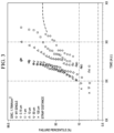
- FIG. 3 presents electromigration (EM) lifetime data for several test structure consistent with the construction of the example of FIG. 1 A , wherein the distance between strapping vias is different for each test structure;
- EM electromigration
- FIG. 4 show EM median lifetime in arbitrary units for the test structures presented in FIG. 3 ;
- FIG. 5 illustrates a sectional view of a test device that includes strapping vias landing on the bottom metal level of a device similar to that shown in FIG. 1 A , with the top level metal omitted such that all current flows in the bottom metal level;
- FIG. 6 presents the EM lifetime data of FIG. 3 , including additional EM lifetime data for the structure of FIG. 5 ;
- FIG. 7 schematically illustrates copper diffusion paths between spaced-apart vias contacting a wide metal line
- FIG. 8 A shows portions of a narrow strapped interconnect structure consistent with conventional practice, while inset FIG. 8 B shows a conventional overlap between the metal line and a strapping via;
- FIG. 11 A shows portions of a wide strapped interconnect structure consistent with the disclosure including spaced apart strapping bar vias, while inset FIG. 11 B shows zero overlap between the metal line and the bar via;
- the present disclosure provides strapped interconnect lines that may have as much as five times or more the electromigration (EM) lifetime as conventional strapped interconnect lines of the same dimensions.
- the interconnect lines are strapped by vias that not only shunt current between the strapped lines, but also reduce diffusion of metal atoms in the interconnect lines.
- the described examples may require little or no modification of existing process flows, and are expected to provide enhanced current carrying capability beneficial for advanced power devices with low on-resistance.
- metal interconnect lines are strapped together by vias that span the width of the lines and are spaced closely together. Such structures have been found to effectively suppress copper diffusion under high current density, as further described below, thus providing an effective alternative to known methods of improving EM lifetime in strapped interconnect lines.
- Copper interconnects have a different EM diffusion path as compared to aluminum interconnects.
- the major diffusion path of aluminum in the interconnect is understood to occur along grain boundaries.
- diffusion of copper in copper interconnects is understood to occur along an interface between the copper line and an overlying dielectric capping layer, e.g. silicon nitride, that is typically used in copper damascene structures.
- dielectric capping layer e.g. silicon nitride
- the inventors have determined that an alternative method of increasing EM lifetime is possible with copper interconnects while allowing for long interconnect lines in power devices or other integrated circuits. Because copper diffusion occurs along the surface of the interconnect line, atomic diffusion may be limited by periodically blocking the diffusion path along the surface. As described in greater detail below, the inventors have discovered that the copper diffusion path may be limited to the Blech length or less by periodically interrupting the copper-dielectric cap interface of a lower-level line with a barrier metal used to form an overlying copper via used to strap the lower line to an overlying line. By spacing the vias close together the effective length of the diffusion path may be limited to the distance between the vias, and electromigration of the copper may be significantly reduced, thereby increasing the EM lifetime.
- FIG. 1 A illustrates an example integrated circuit (IC) 100 including a copper interconnect system.
- a semiconductor substrate 105 supports a dielectric layer 110 , such as pre-metal dielectric.
- the substrate 105 may include silicon, germanium, gallium arsenide, or gallium nitride, for example.
- the IC 100 may include transistors (not shown) formed in or over the semiconductor substrate.
- a first line 115 at a first metal level, e.g. metal 1 (M1) is strapped to a second metal line 125 at a second metal level, e.g. metal 2 (M2) by a plurality of strapping vias 120 .
- M1 first metal level
- M2 second metal level
- the combined structure including first line 115 , second line 125 and strapping vias 120 may be referred to as a strapped interconnect line 150 .
- the strapping vias 120 are spaced apart along the strapped interconnect line 150 by a strap distance L.
- a metal line 140 at the metal 3 (M3) level may source current to a source end of the strapped interconnect line 150 by way of vias 130
- a metal line 145 at the M3 level may sink the current and a sink end of the strapped interconnect line 150 by way of additional vias 130 .
- One or both of the metal lines 140 and 145 may be connected directly or indirectly to a transistor that sources or sinks the current.
- the illustrated interconnection is shown without implied limitation as a representation of the general structure having enhanced EM lifetime as described herein.
- the first and second metal levels may be at other metallization levels of the IC 100 , such as M2/M3, M3/M4, M4/M5, etc.
- the source line and sink line may be absent in some other examples in which the strapped interconnect line 150 is connected directly by metal contacts at one or both ends to a corresponding transistor.
- each of the vias 120 is spaced apart from a nearest neighbor via 120 by a segment 135 of a capping dielectric, e.g. silicon nitride, silicon carbonitride, or other suitable dielectric copper barrier.
- a capping dielectric e.g. silicon nitride, silicon carbonitride, or other suitable dielectric copper barrier.
- Each via 120 has a first axis parallel to the direction of current flow in the first line 115 , and a second axis normal to the short axis that substantially spans the width of the first metal line 115 .
- substantially spans it is meant that the second axis of the via 120 is at least 90% the width of the first metal line 115 . In some examples the length of the second axis is equal to or greater than the width of the first metal line 115 .
- the vias 120 may have an aspect ratio, e.g. the ratio of the second axis length to the first axis length, of unity (square), larger than unity, e.g. two or greater, or less than unity. Vias 120 with an aspect ratio greater or less than unity may be referred to as a “bar via”.
- FIG. 2 illustrates a sectional view of a single strapping via 120 , showing some additional layers that are typically present in a copper interconnect.
- copper interconnects may be formed by a damascene process in which copper is electroplated into recesses in a dielectric layer. The copper is typically then polished back to the dielectric surface to define individual traces.
- the damascene technique typically includes various liners and capping layers, e.g. to serve as an electroplating base, to prevent copper diffusion and/or to improve adhesion.
- FIG. 1 illustrates a sectional view of a single strapping via 120 , showing some additional layers that are typically present in a copper interconnect.
- Dielectric cap segments 135 contact the line 115 outside the contact area of the via 120 , and a dielectric cap layer 250 that may have a same composition as the dielectric cap segments 135 caps the line 125 .
- the dielectric cap segments and the dielectric cap layer 250 may substantially comprise plasma-deposited silicon nitride.
- copper diffusion is understood to occur along the interface between the line 115 and the dielectric cap segments 135 , or along the line 125 and the dielectric cap layer 250 . It is believed that diffusion is substantially blocked along the line 115 where the tantalum liner 230 contacts the line 115 . It is further believed that reducing this diffusion is sufficient to provide significant improvement of the EM lifetime of the strapped interconnect line 150 , even if diffusion along the line 125 is not affected.
- FIG. 3 illustrates a log-normal probability plot of time-to-fail for populations of the 0.16 ⁇ m test devices.
- This figure shows a clear relationship between the strap distance L and the EM lifetime of the test devices.
- the test devices with a strap distance of 50 ⁇ m or greater essentially showed the same EM lifetime, while the EM lifetime becomes progressively greater for a strap distance of 10 ⁇ m, 1.0 ⁇ m and 0.15 ⁇ m.
- some of the test devices with a strap distance of 0.15 ⁇ m did not fail at all under these test conditions, so-called “immortal” devices.
- FIG. 1 illustrates a log-normal probability plot of time-to-fail for populations of the 0.16 ⁇ m test devices.
- the increased EM lifetime of the test devices with decreasing strap distance is understood to be due at least in part to blocking copper diffusion along the top of the copper lines by the tantalum liner 230 of each strapping via 120 .
- PFA analysis of some of the devices with strap distance equal to 0.15 ⁇ m showed voiding in the M2 line 125 , but not the M1 line 115 , consistent with the understanding that diffusion along the M1 line is effectively suppressed by the short strap distance L, and that protecting the M1 line is sufficient to significantly increase the EM lifetime of the strapped interconnect line 150 .
- FIG. 5 shows the M1 line 115 similar to FIG. 1 A , but omits the substrate 105 and dielectric layer 110 and the source/sink lines 140 , 145 for brevity.
- the strapping vias 120 are spaced along the M1 line 115 as in FIG. 1 A , but the M2 line 125 is replaced by M2 islands 510 .
- no current flows through the M2 layer or the strapping vias 120 but the tantalum liner 230 associated with strapping vias 120 continue to suppress diffusion along the M1 line 115 .
- the test structure 500 was characterized only for the case that the strap distance L is 1 ⁇ m.
- the test current was not compensated to account for elimination of the M2 layer as a current path, so the current density in the M1 layer 115 was twice the other test devices.
- FIG. 6 shows the EM lifetimes of such devices 500 overlaid on the data of FIG. 3 . Even with the greater current density through the M1 layer 115 , the EM lifetime of the device 500 showed a clear increase, providing further confirmation of the role of the tantalum liner 230 in suppressing copper diffusion along the surface of the M1 line 115 .
- FIG. 7 illustrates spaced-apart vias on a wide line, e.g. about 1 ⁇ m.
- a wide line e.g. about 1 ⁇ m.
- columns of multiple square strapping vias may be conventionally placed along a long strapped line.
- closely spacing the via columns along a 1 ⁇ m line provided no measurable improvement of EM lifetime of the wide line. This result is understood to support the conclusion that gaps between the strapping vias allow copper diffusion to occur at a sufficient rate that the copper diffusion is not limited to a distance similar to the Blech length. This effect is illustrated schematically in FIG.
- the synergistic effect of the strapping vias that extend completely from one side of the strapped line to the opposite side of the strapped line is an unexpected result, and to the inventors' knowledge a hitherto unobserved effect, wherein the maximum sustainable current for a strapped interconnect line 150 is greater than the sum of the maximum sustained current through each individual interconnect line, e.g. the lines 115 and 125 .
- This effect allows the strapped interconnect line 150 to be narrower than conventionally possible for a given current-carrying capacity, which in turn allows for a reduced die size of the IC of which the strapped interconnect line 150 is a part.
- FIGS. 9 A / 9 B illustrate a narrow strapped line 910 that includes M1 and M2 lines connected to an M3 feeder 920 .
- the M1 and M2 lines are connected by strapping vias 930 that extend continuously from one side of the strapped line 910 to the opposite side of the strapped line 910 , according to the disclosure.
- the EM lifetime of the strapped line 910 is expected to be significantly larger than that of the strapped line 810 when the spacing between the strapping vias 930 is less than 10 ⁇ m.
- FIGS. 10 A / 10 B illustrate a wide strapped line 1010 that includes M1 and M2 lines connected to an M3 feeder 1020 .
- the M1 and M2 lines are connected by strapping vias 1030 that are conventionally spaced apart from each other and from sides of the strapped line 1010 by a nonzero value. Again, such spaces allow copper diffusion around the vias 1030 , with resulting reduced EM lifetime of the wide strapped line 1010 .
- the spacing of the strapping vias 1130 along the strapped line 1110 indicates greater benefit is conferred when the vias 1130 are no further apart than the Blech length. Since this length may be difficult to precisely determine, the strapping vias 1130 may be spaced as closely as allowed by the applicable design rules. In some examples this minimum spacing may be about equal to the width of the strapping vias 1130 , e.g. about 0.15 ⁇ m in the current example. However, as demonstrated by FIG. 3 , benefit may be obtained when the spacing between the strapping vias 1130 is no greater than 10 ⁇ m.
Landscapes
- Physics & Mathematics (AREA)
- Electromagnetism (AREA)
- Engineering & Computer Science (AREA)
- Microelectronics & Electronic Packaging (AREA)
- Health & Medical Sciences (AREA)
- Toxicology (AREA)
- Internal Circuitry In Semiconductor Integrated Circuit Devices (AREA)
- Design And Manufacture Of Integrated Circuits (AREA)
Abstract
Description
Claims (28)
Priority Applications (1)
| Application Number | Priority Date | Filing Date | Title |
|---|---|---|---|
| US17/176,995 US12027468B2 (en) | 2020-02-13 | 2021-02-16 | Strapped copper interconnect for improved electromigration reliability |
Applications Claiming Priority (3)
| Application Number | Priority Date | Filing Date | Title |
|---|---|---|---|
| US202062975844P | 2020-02-13 | 2020-02-13 | |
| US202062982168P | 2020-02-27 | 2020-02-27 | |
| US17/176,995 US12027468B2 (en) | 2020-02-13 | 2021-02-16 | Strapped copper interconnect for improved electromigration reliability |
Publications (2)
| Publication Number | Publication Date |
|---|---|
| US20210257312A1 US20210257312A1 (en) | 2021-08-19 |
| US12027468B2 true US12027468B2 (en) | 2024-07-02 |
Family
ID=77273056
Family Applications (1)
| Application Number | Title | Priority Date | Filing Date |
|---|---|---|---|
| US17/176,995 Active 2041-08-08 US12027468B2 (en) | 2020-02-13 | 2021-02-16 | Strapped copper interconnect for improved electromigration reliability |
Country Status (1)
| Country | Link |
|---|---|
| US (1) | US12027468B2 (en) |
Citations (5)
| Publication number | Priority date | Publication date | Assignee | Title |
|---|---|---|---|---|
| US5767546A (en) | 1994-12-30 | 1998-06-16 | Siliconix Incorporated | Laternal power mosfet having metal strap layer to reduce distributed resistance |
| US20060289994A1 (en) * | 2005-06-24 | 2006-12-28 | International Business Machines Corporation | Multi-level interconnections for an integrated circuit chip |
| US10189705B1 (en) * | 2017-10-25 | 2019-01-29 | Globalfoundries Singapore Pte. Ltd. | Monolithic integration of MEMS and IC devices |
| US20200111736A1 (en) * | 2018-10-08 | 2020-04-09 | International Business Machines Corporation | Skip via for metal interconnects |
| US20200327208A1 (en) * | 2019-04-12 | 2020-10-15 | International Business Machines Corporation | Via design optimization to improve via resistance |
-
2021
- 2021-02-16 US US17/176,995 patent/US12027468B2/en active Active
Patent Citations (5)
| Publication number | Priority date | Publication date | Assignee | Title |
|---|---|---|---|---|
| US5767546A (en) | 1994-12-30 | 1998-06-16 | Siliconix Incorporated | Laternal power mosfet having metal strap layer to reduce distributed resistance |
| US20060289994A1 (en) * | 2005-06-24 | 2006-12-28 | International Business Machines Corporation | Multi-level interconnections for an integrated circuit chip |
| US10189705B1 (en) * | 2017-10-25 | 2019-01-29 | Globalfoundries Singapore Pte. Ltd. | Monolithic integration of MEMS and IC devices |
| US20200111736A1 (en) * | 2018-10-08 | 2020-04-09 | International Business Machines Corporation | Skip via for metal interconnects |
| US20200327208A1 (en) * | 2019-04-12 | 2020-10-15 | International Business Machines Corporation | Via design optimization to improve via resistance |
Non-Patent Citations (8)
| Title |
|---|
| "A Novel Self-Aligned Surface-Silicide Passivation Technology for Reliability Enhancement in Copper Interconnects", Takewaki et al., 1995 Symposium on VLSI Technology Digest of Technical Papers, p. 31-32. |
| "Comparison of Cu electromigration lifetime in Cu interconnects coated with various caps", Appl. Phys. Lett. 83, 869 (2003); https://doi.org/10.1063/1.1596375. |
| "Current Crowding Impact on Electromigration in AI Interconnects", Park et al., Analog Technology Development, Texas Instruments, Dallas, TX, U.S.A. |
| "Electromigration Current Limit Relaxation for Power Device Interconnects", Joh et al., Proceedings of the 30th International Symposium on Power Semiconductor Devices & ICs May 13-17, 2018, Chicago, USA, p. 68-71. |
| "Electromigration in thin aluminum films on titanium nitride", J. Appl. Phys., vol. 47, No. 4, Apr. 1976. |
| "Electromigration path in Cu thin-film lines", Appl. Phys. Lett., vol. 74, No. 20, May 17, 1999. |
| "Lateral Smart-Discrete Process and Devices based on Thin-Layer Silicon-on-Insulator", Letavic et al., Proceedings of 2001 International Symposium on Power Semiconductor Devices & ICs, Osaka, p. 407-410. |
| "Relationship between interfacial adhesion and electromigration in Cu metallization", Journal of Applied Physics 93, 1417 (2003); https://doi.org/10.1063/1.1532942. |
Also Published As
| Publication number | Publication date |
|---|---|
| US20210257312A1 (en) | 2021-08-19 |
Similar Documents
| Publication | Publication Date | Title |
|---|---|---|
| EP1387404B1 (en) | Semiconductor device | |
| US7439173B2 (en) | Increasing electromigration lifetime and current density in IC using vertically upwardly extending dummy via | |
| US8435802B2 (en) | Conductor layout technique to reduce stress-induced void formations | |
| US10218346B1 (en) | High current lateral GaN transistors with scalable topology and gate drive phase equalization | |
| TWI473231B (en) | Interconnect structure of integrated circuit with improved electromigration characteristics | |
| US9929087B2 (en) | Enhancing integrated circuit density with active atomic reservoir | |
| US20070182001A1 (en) | Semiconductor device | |
| US20080203562A1 (en) | Method for designing semiconductor device and semiconductor device | |
| US20150340315A1 (en) | Semiconductor device | |
| US20170256449A1 (en) | Methods of forming conductive structures with different material compositions in a metallization layer | |
| JP5097501B2 (en) | Manufacturing method of semiconductor integrated circuit device | |
| US12027468B2 (en) | Strapped copper interconnect for improved electromigration reliability | |
| US7155686B2 (en) | Placement and routing method to reduce Joule heating | |
| US10950540B2 (en) | Enhancing integrated circuit density with active atomic reservoir | |
| US20080203495A1 (en) | Integration circuits for reducing electromigration effect | |
| KR100764054B1 (en) | Metal wiring and forming method | |
| US20240113013A1 (en) | Semiconductor structures with stacked interconnects |
Legal Events
| Date | Code | Title | Description |
|---|---|---|---|
| STPP | Information on status: patent application and granting procedure in general |
Free format text: APPLICATION DISPATCHED FROM PREEXAM, NOT YET DOCKETED |
|
| STPP | Information on status: patent application and granting procedure in general |
Free format text: DOCKETED NEW CASE - READY FOR EXAMINATION |
|
| STPP | Information on status: patent application and granting procedure in general |
Free format text: NON FINAL ACTION MAILED |
|
| STPP | Information on status: patent application and granting procedure in general |
Free format text: FINAL REJECTION MAILED |
|
| STCV | Information on status: appeal procedure |
Free format text: NOTICE OF APPEAL FILED |
|
| STCV | Information on status: appeal procedure |
Free format text: APPEAL BRIEF (OR SUPPLEMENTAL BRIEF) ENTERED AND FORWARDED TO EXAMINER |
|
| STCV | Information on status: appeal procedure |
Free format text: EXAMINER'S ANSWER TO APPEAL BRIEF MAILED |
|
| STPP | Information on status: patent application and granting procedure in general |
Free format text: DOCKETED NEW CASE - READY FOR EXAMINATION |
|
| STPP | Information on status: patent application and granting procedure in general |
Free format text: NOTICE OF ALLOWANCE MAILED -- APPLICATION RECEIVED IN OFFICE OF PUBLICATIONS |
|
| STPP | Information on status: patent application and granting procedure in general |
Free format text: NOTICE OF ALLOWANCE MAILED -- APPLICATION RECEIVED IN OFFICE OF PUBLICATIONS |
|
| AS | Assignment |
Owner name: TEXAS INSTRUMENTS INCORPORATED, TEXAS Free format text: ASSIGNMENT OF ASSIGNORS INTEREST;ASSIGNORS:JOH, JUNGWOO;PARK, YOUNG-JOON;REEL/FRAME:067505/0662 Effective date: 20210216 |
|
| STPP | Information on status: patent application and granting procedure in general |
Free format text: PUBLICATIONS -- ISSUE FEE PAYMENT VERIFIED |
|
| STCF | Information on status: patent grant |
Free format text: PATENTED CASE |