US12019376B2 - Polymer brush adhesion promoter with UV cleavable linker - Google Patents
Polymer brush adhesion promoter with UV cleavable linker Download PDFInfo
- Publication number
- US12019376B2 US12019376B2 US17/507,933 US202117507933A US12019376B2 US 12019376 B2 US12019376 B2 US 12019376B2 US 202117507933 A US202117507933 A US 202117507933A US 12019376 B2 US12019376 B2 US 12019376B2
- Authority
- US
- United States
- Prior art keywords
- semiconductor structure
- cleavable linker
- hardmask
- polymer brush
- developer
- Prior art date
- Legal status (The legal status is an assumption and is not a legal conclusion. Google has not performed a legal analysis and makes no representation as to the accuracy of the status listed.)
- Active, expires
Links
- 229920000642 polymer Polymers 0.000 title claims abstract description 65
- 239000002318 adhesion promoter Substances 0.000 title description 7
- 239000013545 self-assembled monolayer Substances 0.000 claims description 42
- 239000002094 self assembled monolayer Substances 0.000 claims description 37
- 239000004065 semiconductor Substances 0.000 claims description 35
- 239000010410 layer Substances 0.000 claims description 31
- KFZMGEQAYNKOFK-UHFFFAOYSA-N Isopropanol Chemical group CC(C)O KFZMGEQAYNKOFK-UHFFFAOYSA-N 0.000 claims description 21
- WGTYBPLFGIVFAS-UHFFFAOYSA-M tetramethylammonium hydroxide Chemical group [OH-].C[N+](C)(C)C WGTYBPLFGIVFAS-UHFFFAOYSA-M 0.000 claims description 16
- 229960004592 isopropanol Drugs 0.000 claims description 7
- XLYOFNOQVPJJNP-UHFFFAOYSA-N water Substances O XLYOFNOQVPJJNP-UHFFFAOYSA-N 0.000 claims description 6
- 238000000034 method Methods 0.000 abstract description 27
- 239000002904 solvent Substances 0.000 abstract description 8
- 238000004519 manufacturing process Methods 0.000 abstract description 4
- 238000000151 deposition Methods 0.000 abstract description 3
- 239000000758 substrate Substances 0.000 description 21
- 230000008569 process Effects 0.000 description 11
- 229910000577 Silicon-germanium Inorganic materials 0.000 description 10
- 239000000463 material Substances 0.000 description 9
- 235000012431 wafers Nutrition 0.000 description 8
- XUIMIQQOPSSXEZ-UHFFFAOYSA-N Silicon Chemical compound [Si] XUIMIQQOPSSXEZ-UHFFFAOYSA-N 0.000 description 7
- 150000001875 compounds Chemical class 0.000 description 7
- 229910052710 silicon Inorganic materials 0.000 description 7
- 239000010703 silicon Substances 0.000 description 7
- 229910052581 Si3N4 Inorganic materials 0.000 description 5
- 238000013461 design Methods 0.000 description 5
- HQVNEWCFYHHQES-UHFFFAOYSA-N silicon nitride Chemical compound N12[Si]34N5[Si]62N3[Si]51N64 HQVNEWCFYHHQES-UHFFFAOYSA-N 0.000 description 4
- LEVVHYCKPQWKOP-UHFFFAOYSA-N [Si].[Ge] Chemical compound [Si].[Ge] LEVVHYCKPQWKOP-UHFFFAOYSA-N 0.000 description 3
- 238000000576 coating method Methods 0.000 description 3
- 238000001900 extreme ultraviolet lithography Methods 0.000 description 3
- 230000003993 interaction Effects 0.000 description 3
- 238000001459 lithography Methods 0.000 description 3
- 229920006254 polymer film Polymers 0.000 description 3
- 238000000682 scanning probe acoustic microscopy Methods 0.000 description 3
- 238000003860 storage Methods 0.000 description 3
- 239000000126 substance Substances 0.000 description 3
- OKTJSMMVPCPJKN-UHFFFAOYSA-N Carbon Chemical compound [C] OKTJSMMVPCPJKN-UHFFFAOYSA-N 0.000 description 2
- 229910001218 Gallium arsenide Inorganic materials 0.000 description 2
- 108091034117 Oligonucleotide Proteins 0.000 description 2
- 238000000429 assembly Methods 0.000 description 2
- 230000000712 assembly Effects 0.000 description 2
- 238000001505 atmospheric-pressure chemical vapour deposition Methods 0.000 description 2
- 239000011324 bead Substances 0.000 description 2
- 229910052799 carbon Inorganic materials 0.000 description 2
- 239000007795 chemical reaction product Substances 0.000 description 2
- 239000011248 coating agent Substances 0.000 description 2
- 238000011161 development Methods 0.000 description 2
- 239000000975 dye Substances 0.000 description 2
- 230000001939 inductive effect Effects 0.000 description 2
- 239000012212 insulator Substances 0.000 description 2
- 238000004518 low pressure chemical vapour deposition Methods 0.000 description 2
- 238000012986 modification Methods 0.000 description 2
- 230000004048 modification Effects 0.000 description 2
- 238000000623 plasma-assisted chemical vapour deposition Methods 0.000 description 2
- 238000002360 preparation method Methods 0.000 description 2
- 239000000047 product Substances 0.000 description 2
- 239000000523 sample Substances 0.000 description 2
- HBMJWWWQQXIZIP-UHFFFAOYSA-N silicon carbide Chemical compound [Si+]#[C-] HBMJWWWQQXIZIP-UHFFFAOYSA-N 0.000 description 2
- 238000001179 sorption measurement Methods 0.000 description 2
- 239000004094 surface-active agent Substances 0.000 description 2
- 238000012876 topography Methods 0.000 description 2
- 238000012546 transfer Methods 0.000 description 2
- 229910000980 Aluminium gallium arsenide Inorganic materials 0.000 description 1
- 229910000673 Indium arsenide Inorganic materials 0.000 description 1
- 229910020751 SixGe1-x Inorganic materials 0.000 description 1
- 229910007709 ZnTe Inorganic materials 0.000 description 1
- JLCPHMBAVCMARE-UHFFFAOYSA-N [3-[[3-[[3-[[3-[[3-[[3-[[3-[[3-[[3-[[3-[[3-[[5-(2-amino-6-oxo-1H-purin-9-yl)-3-[[3-[[3-[[3-[[3-[[3-[[5-(2-amino-6-oxo-1H-purin-9-yl)-3-[[5-(2-amino-6-oxo-1H-purin-9-yl)-3-hydroxyoxolan-2-yl]methoxy-hydroxyphosphoryl]oxyoxolan-2-yl]methoxy-hydroxyphosphoryl]oxy-5-(5-methyl-2,4-dioxopyrimidin-1-yl)oxolan-2-yl]methoxy-hydroxyphosphoryl]oxy-5-(6-aminopurin-9-yl)oxolan-2-yl]methoxy-hydroxyphosphoryl]oxy-5-(6-aminopurin-9-yl)oxolan-2-yl]methoxy-hydroxyphosphoryl]oxy-5-(6-aminopurin-9-yl)oxolan-2-yl]methoxy-hydroxyphosphoryl]oxy-5-(6-aminopurin-9-yl)oxolan-2-yl]methoxy-hydroxyphosphoryl]oxyoxolan-2-yl]methoxy-hydroxyphosphoryl]oxy-5-(5-methyl-2,4-dioxopyrimidin-1-yl)oxolan-2-yl]methoxy-hydroxyphosphoryl]oxy-5-(4-amino-2-oxopyrimidin-1-yl)oxolan-2-yl]methoxy-hydroxyphosphoryl]oxy-5-(5-methyl-2,4-dioxopyrimidin-1-yl)oxolan-2-yl]methoxy-hydroxyphosphoryl]oxy-5-(5-methyl-2,4-dioxopyrimidin-1-yl)oxolan-2-yl]methoxy-hydroxyphosphoryl]oxy-5-(6-aminopurin-9-yl)oxolan-2-yl]methoxy-hydroxyphosphoryl]oxy-5-(6-aminopurin-9-yl)oxolan-2-yl]methoxy-hydroxyphosphoryl]oxy-5-(4-amino-2-oxopyrimidin-1-yl)oxolan-2-yl]methoxy-hydroxyphosphoryl]oxy-5-(4-amino-2-oxopyrimidin-1-yl)oxolan-2-yl]methoxy-hydroxyphosphoryl]oxy-5-(4-amino-2-oxopyrimidin-1-yl)oxolan-2-yl]methoxy-hydroxyphosphoryl]oxy-5-(6-aminopurin-9-yl)oxolan-2-yl]methoxy-hydroxyphosphoryl]oxy-5-(4-amino-2-oxopyrimidin-1-yl)oxolan-2-yl]methyl [5-(6-aminopurin-9-yl)-2-(hydroxymethyl)oxolan-3-yl] hydrogen phosphate Polymers Cc1cn(C2CC(OP(O)(=O)OCC3OC(CC3OP(O)(=O)OCC3OC(CC3O)n3cnc4c3nc(N)[nH]c4=O)n3cnc4c3nc(N)[nH]c4=O)C(COP(O)(=O)OC3CC(OC3COP(O)(=O)OC3CC(OC3COP(O)(=O)OC3CC(OC3COP(O)(=O)OC3CC(OC3COP(O)(=O)OC3CC(OC3COP(O)(=O)OC3CC(OC3COP(O)(=O)OC3CC(OC3COP(O)(=O)OC3CC(OC3COP(O)(=O)OC3CC(OC3COP(O)(=O)OC3CC(OC3COP(O)(=O)OC3CC(OC3COP(O)(=O)OC3CC(OC3COP(O)(=O)OC3CC(OC3COP(O)(=O)OC3CC(OC3COP(O)(=O)OC3CC(OC3COP(O)(=O)OC3CC(OC3COP(O)(=O)OC3CC(OC3CO)n3cnc4c(N)ncnc34)n3ccc(N)nc3=O)n3cnc4c(N)ncnc34)n3ccc(N)nc3=O)n3ccc(N)nc3=O)n3ccc(N)nc3=O)n3cnc4c(N)ncnc34)n3cnc4c(N)ncnc34)n3cc(C)c(=O)[nH]c3=O)n3cc(C)c(=O)[nH]c3=O)n3ccc(N)nc3=O)n3cc(C)c(=O)[nH]c3=O)n3cnc4c3nc(N)[nH]c4=O)n3cnc4c(N)ncnc34)n3cnc4c(N)ncnc34)n3cnc4c(N)ncnc34)n3cnc4c(N)ncnc34)O2)c(=O)[nH]c1=O JLCPHMBAVCMARE-UHFFFAOYSA-N 0.000 description 1
- 238000010521 absorption reaction Methods 0.000 description 1
- 239000002253 acid Substances 0.000 description 1
- 229910045601 alloy Inorganic materials 0.000 description 1
- 239000000956 alloy Substances 0.000 description 1
- ISQINHMJILFLAQ-UHFFFAOYSA-N argon hydrofluoride Chemical compound F.[Ar] ISQINHMJILFLAQ-UHFFFAOYSA-N 0.000 description 1
- 230000004888 barrier function Effects 0.000 description 1
- 230000015572 biosynthetic process Effects 0.000 description 1
- 239000000919 ceramic Substances 0.000 description 1
- 150000005829 chemical entities Chemical class 0.000 description 1
- 238000006243 chemical reaction Methods 0.000 description 1
- 238000005229 chemical vapour deposition Methods 0.000 description 1
- 239000000470 constituent Substances 0.000 description 1
- 239000000356 contaminant Substances 0.000 description 1
- 238000000354 decomposition reaction Methods 0.000 description 1
- 238000001514 detection method Methods 0.000 description 1
- 239000003989 dielectric material Substances 0.000 description 1
- 238000006471 dimerization reaction Methods 0.000 description 1
- 238000007772 electroless plating Methods 0.000 description 1
- 238000009713 electroplating Methods 0.000 description 1
- 238000005530 etching Methods 0.000 description 1
- 230000008020 evaporation Effects 0.000 description 1
- 238000001704 evaporation Methods 0.000 description 1
- 230000006870 function Effects 0.000 description 1
- 125000000524 functional group Chemical group 0.000 description 1
- 229910052732 germanium Inorganic materials 0.000 description 1
- GNPVGFCGXDBREM-UHFFFAOYSA-N germanium atom Chemical compound [Ge] GNPVGFCGXDBREM-UHFFFAOYSA-N 0.000 description 1
- 230000003760 hair shine Effects 0.000 description 1
- 238000010438 heat treatment Methods 0.000 description 1
- 238000005286 illumination Methods 0.000 description 1
- 238000000671 immersion lithography Methods 0.000 description 1
- RPQDHPTXJYYUPQ-UHFFFAOYSA-N indium arsenide Chemical compound [In]#[As] RPQDHPTXJYYUPQ-UHFFFAOYSA-N 0.000 description 1
- 238000009434 installation Methods 0.000 description 1
- 239000013067 intermediate product Substances 0.000 description 1
- 238000007737 ion beam deposition Methods 0.000 description 1
- 229920002521 macromolecule Polymers 0.000 description 1
- 238000001755 magnetron sputter deposition Methods 0.000 description 1
- 230000007246 mechanism Effects 0.000 description 1
- 239000000155 melt Substances 0.000 description 1
- 239000002184 metal Substances 0.000 description 1
- 238000000813 microcontact printing Methods 0.000 description 1
- 238000004377 microelectronic Methods 0.000 description 1
- 239000000178 monomer Substances 0.000 description 1
- 239000002105 nanoparticle Substances 0.000 description 1
- 150000004767 nitrides Chemical class 0.000 description 1
- 230000003287 optical effect Effects 0.000 description 1
- 239000011368 organic material Substances 0.000 description 1
- 238000000059 patterning Methods 0.000 description 1
- 238000007539 photo-oxidation reaction Methods 0.000 description 1
- 238000000206 photolithography Methods 0.000 description 1
- 229920002120 photoresistant polymer Polymers 0.000 description 1
- 238000005240 physical vapour deposition Methods 0.000 description 1
- 238000005268 plasma chemical vapour deposition Methods 0.000 description 1
- 238000007747 plating Methods 0.000 description 1
- 238000012545 processing Methods 0.000 description 1
- 230000009467 reduction Effects 0.000 description 1
- 230000002829 reductive effect Effects 0.000 description 1
- 238000002310 reflectometry Methods 0.000 description 1
- SBIBMFFZSBJNJF-UHFFFAOYSA-N selenium;zinc Chemical compound [Se]=[Zn] SBIBMFFZSBJNJF-UHFFFAOYSA-N 0.000 description 1
- 238000007086 side reaction Methods 0.000 description 1
- 229910010271 silicon carbide Inorganic materials 0.000 description 1
- 239000002356 single layer Substances 0.000 description 1
- 238000004528 spin coating Methods 0.000 description 1
- 150000003573 thiols Chemical class 0.000 description 1
Images


Classifications
-
- G—PHYSICS
- G03—PHOTOGRAPHY; CINEMATOGRAPHY; ANALOGOUS TECHNIQUES USING WAVES OTHER THAN OPTICAL WAVES; ELECTROGRAPHY; HOLOGRAPHY
- G03F—PHOTOMECHANICAL PRODUCTION OF TEXTURED OR PATTERNED SURFACES, e.g. FOR PRINTING, FOR PROCESSING OF SEMICONDUCTOR DEVICES; MATERIALS THEREFOR; ORIGINALS THEREFOR; APPARATUS SPECIALLY ADAPTED THEREFOR
- G03F7/00—Photomechanical, e.g. photolithographic, production of textured or patterned surfaces, e.g. printing surfaces; Materials therefor, e.g. comprising photoresists; Apparatus specially adapted therefor
- G03F7/004—Photosensitive materials
- G03F7/085—Photosensitive compositions characterised by adhesion-promoting non-macromolecular additives
-
- G—PHYSICS
- G03—PHOTOGRAPHY; CINEMATOGRAPHY; ANALOGOUS TECHNIQUES USING WAVES OTHER THAN OPTICAL WAVES; ELECTROGRAPHY; HOLOGRAPHY
- G03F—PHOTOMECHANICAL PRODUCTION OF TEXTURED OR PATTERNED SURFACES, e.g. FOR PRINTING, FOR PROCESSING OF SEMICONDUCTOR DEVICES; MATERIALS THEREFOR; ORIGINALS THEREFOR; APPARATUS SPECIALLY ADAPTED THEREFOR
- G03F7/00—Photomechanical, e.g. photolithographic, production of textured or patterned surfaces, e.g. printing surfaces; Materials therefor, e.g. comprising photoresists; Apparatus specially adapted therefor
- G03F7/20—Exposure; Apparatus therefor
- G03F7/2002—Exposure; Apparatus therefor with visible light or UV light, through an original having an opaque pattern on a transparent support, e.g. film printing, projection printing; by reflection of visible or UV light from an original such as a printed image
- G03F7/2004—Exposure; Apparatus therefor with visible light or UV light, through an original having an opaque pattern on a transparent support, e.g. film printing, projection printing; by reflection of visible or UV light from an original such as a printed image characterised by the use of a particular light source, e.g. fluorescent lamps or deep UV light
-
- G—PHYSICS
- G03—PHOTOGRAPHY; CINEMATOGRAPHY; ANALOGOUS TECHNIQUES USING WAVES OTHER THAN OPTICAL WAVES; ELECTROGRAPHY; HOLOGRAPHY
- G03F—PHOTOMECHANICAL PRODUCTION OF TEXTURED OR PATTERNED SURFACES, e.g. FOR PRINTING, FOR PROCESSING OF SEMICONDUCTOR DEVICES; MATERIALS THEREFOR; ORIGINALS THEREFOR; APPARATUS SPECIALLY ADAPTED THEREFOR
- G03F7/00—Photomechanical, e.g. photolithographic, production of textured or patterned surfaces, e.g. printing surfaces; Materials therefor, e.g. comprising photoresists; Apparatus specially adapted therefor
- G03F7/004—Photosensitive materials
- G03F7/039—Macromolecular compounds which are photodegradable, e.g. positive electron resists
-
- G—PHYSICS
- G03—PHOTOGRAPHY; CINEMATOGRAPHY; ANALOGOUS TECHNIQUES USING WAVES OTHER THAN OPTICAL WAVES; ELECTROGRAPHY; HOLOGRAPHY
- G03F—PHOTOMECHANICAL PRODUCTION OF TEXTURED OR PATTERNED SURFACES, e.g. FOR PRINTING, FOR PROCESSING OF SEMICONDUCTOR DEVICES; MATERIALS THEREFOR; ORIGINALS THEREFOR; APPARATUS SPECIALLY ADAPTED THEREFOR
- G03F7/00—Photomechanical, e.g. photolithographic, production of textured or patterned surfaces, e.g. printing surfaces; Materials therefor, e.g. comprising photoresists; Apparatus specially adapted therefor
- G03F7/004—Photosensitive materials
- G03F7/09—Photosensitive materials characterised by structural details, e.g. supports, auxiliary layers
- G03F7/095—Photosensitive materials characterised by structural details, e.g. supports, auxiliary layers having more than one photosensitive layer
-
- G—PHYSICS
- G03—PHOTOGRAPHY; CINEMATOGRAPHY; ANALOGOUS TECHNIQUES USING WAVES OTHER THAN OPTICAL WAVES; ELECTROGRAPHY; HOLOGRAPHY
- G03F—PHOTOMECHANICAL PRODUCTION OF TEXTURED OR PATTERNED SURFACES, e.g. FOR PRINTING, FOR PROCESSING OF SEMICONDUCTOR DEVICES; MATERIALS THEREFOR; ORIGINALS THEREFOR; APPARATUS SPECIALLY ADAPTED THEREFOR
- G03F7/00—Photomechanical, e.g. photolithographic, production of textured or patterned surfaces, e.g. printing surfaces; Materials therefor, e.g. comprising photoresists; Apparatus specially adapted therefor
- G03F7/16—Coating processes; Apparatus therefor
- G03F7/165—Monolayers, e.g. Langmuir-Blodgett
-
- G—PHYSICS
- G03—PHOTOGRAPHY; CINEMATOGRAPHY; ANALOGOUS TECHNIQUES USING WAVES OTHER THAN OPTICAL WAVES; ELECTROGRAPHY; HOLOGRAPHY
- G03F—PHOTOMECHANICAL PRODUCTION OF TEXTURED OR PATTERNED SURFACES, e.g. FOR PRINTING, FOR PROCESSING OF SEMICONDUCTOR DEVICES; MATERIALS THEREFOR; ORIGINALS THEREFOR; APPARATUS SPECIALLY ADAPTED THEREFOR
- G03F7/00—Photomechanical, e.g. photolithographic, production of textured or patterned surfaces, e.g. printing surfaces; Materials therefor, e.g. comprising photoresists; Apparatus specially adapted therefor
- G03F7/20—Exposure; Apparatus therefor
- G03F7/2022—Multi-step exposure, e.g. hybrid; backside exposure; blanket exposure, e.g. for image reversal; edge exposure, e.g. for edge bead removal; corrective exposure
-
- G—PHYSICS
- G03—PHOTOGRAPHY; CINEMATOGRAPHY; ANALOGOUS TECHNIQUES USING WAVES OTHER THAN OPTICAL WAVES; ELECTROGRAPHY; HOLOGRAPHY
- G03F—PHOTOMECHANICAL PRODUCTION OF TEXTURED OR PATTERNED SURFACES, e.g. FOR PRINTING, FOR PROCESSING OF SEMICONDUCTOR DEVICES; MATERIALS THEREFOR; ORIGINALS THEREFOR; APPARATUS SPECIALLY ADAPTED THEREFOR
- G03F7/00—Photomechanical, e.g. photolithographic, production of textured or patterned surfaces, e.g. printing surfaces; Materials therefor, e.g. comprising photoresists; Apparatus specially adapted therefor
- G03F7/26—Processing photosensitive materials; Apparatus therefor
- G03F7/30—Imagewise removal using liquid means
- G03F7/32—Liquid compositions therefor, e.g. developers
- G03F7/322—Aqueous alkaline compositions
-
- G—PHYSICS
- G03—PHOTOGRAPHY; CINEMATOGRAPHY; ANALOGOUS TECHNIQUES USING WAVES OTHER THAN OPTICAL WAVES; ELECTROGRAPHY; HOLOGRAPHY
- G03F—PHOTOMECHANICAL PRODUCTION OF TEXTURED OR PATTERNED SURFACES, e.g. FOR PRINTING, FOR PROCESSING OF SEMICONDUCTOR DEVICES; MATERIALS THEREFOR; ORIGINALS THEREFOR; APPARATUS SPECIALLY ADAPTED THEREFOR
- G03F7/00—Photomechanical, e.g. photolithographic, production of textured or patterned surfaces, e.g. printing surfaces; Materials therefor, e.g. comprising photoresists; Apparatus specially adapted therefor
- G03F7/26—Processing photosensitive materials; Apparatus therefor
- G03F7/30—Imagewise removal using liquid means
- G03F7/32—Liquid compositions therefor, e.g. developers
- G03F7/325—Non-aqueous compositions
Definitions
- the present invention relates generally to surface coatings, and more specifically, to a polymer brush or self-assembled monolayer (SAM) adhesion promoter with an ultraviolet (UV) cleavable linker.
- SAM self-assembled monolayer
- a method for making an adhesion layer of an extreme ultraviolet (EUV) stack.
- the method includes grafting an ultraviolet (UV) sensitive polymer brush on a hardmask, the polymer brush including a UV cleavable unit, depositing EUV resist over the polymer brush, exposing the EUV resist to remove the EUV resist in exposed areas by applying a developer, and flooding the exposed area with a UV light and a solvent developer to remove exposed portions of the polymer brush.
- UV ultraviolet
- a method for making an adhesion layer of an extreme ultraviolet (EUV) stack.
- the method includes grafting a self-assembled monolayer (SAM) on a hardmask, the SAM including an ultraviolet (UV) cleavable unit, depositing EUV resist over the SAM, exposing the EUV resist to remove the EUV resist in exposed areas by applying a developer, and flooding the exposed area with a UV light and a solvent developer to remove exposed portions of the SAM.
- SAM self-assembled monolayer
- UV ultraviolet
- a semiconductor device for making an adhesion layer of an extreme ultraviolet (EUV) stack.
- the semiconductor device includes an ultraviolet (UV) sensitive polymer brush grafted on a hardmask, the polymer brush including a UV cleavable unit, EUV resist disposed over the polymer brush, an opening in the EUV resist formed by applying a developer, the opening defining an exposed area, and a UV light flooding the exposed area and a solvent developer to remove exposed portions of the polymer brush.
- UV ultraviolet
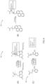
- FIG. 1 is a cross-sectional view of an extreme ultraviolet (EUV) stack, in accordance with an embodiment of the present invention
- FIG. 2 is a polymer brush as an adhesion promoter
- FIG. 3 is a polymer brush with an ultraviolet (UV) cleavable moiety in the polymer chain or self-assembled monolayer (SAM) close to the binding group, in accordance with an embodiment of the present invention
- FIG. 4 is a process for forming the polymer brush with the UV cleavable moiety in the polymer chain or SAM close to the binding group, in accordance with an embodiment of the present invention
- FIG. 5 is a method for forming the polymer brush with the UV cleavable moiety in the polymer chain or SAM close to the binding group, in accordance with an embodiment of the present invention.
- FIG. 6 illustrates exemplary UV cleavable moieties, in accordance with an embodiment of the present invention.
- Embodiments in accordance with the present invention provide methods and devices for making a polymer brush or self-assembled monolayer (SAM) including an ultraviolet (UV) cleavable unit close to the binding site near a hardmask of an extreme ultraviolet (EUV) quad stack.
- the UV cleavable unit can be a UV cleavable moiety or linker in the polymer chain or SAM close to the binding group, where the polymer brush/SAM can act as an adhesion promoter during EUV exposure.
- Flood exposure is employed to develop the polymer brush or SAM post EUV exposure to reduce scumming without sacrificing adhesion capability.
- the flood exposure cleaves the bond and liberates major polymer chains/SAM molecules, thus leaving a thin layer that allows for an easy pattern transfer.
- the flood exposure further enables cleavable linker removal along with the residue or scumming.
- FIG. 1 is a cross-sectional view of an extreme ultraviolet (EUV) stack, in accordance with an embodiment of the present invention.
- EUV extreme ultraviolet
- a semiconductor structure 5 includes a substrate 10 , an organic planarization layer (OPL) 12 formed over the substrate 10 , and a hardmask 14 formed over the OPL 12 .
- An adhesion layer 16 can be formed over the hardmask 14 .
- the EUV quad stack needs an adhesion layer 16 for patterning.
- An EUV resist 18 is then formed over the adhesion layer 16 .
- EUV lithography uses an EUV light of an extremely short wavelength of 13.5 nm. EUV lithography allows exposure of fine circuit patterns with a half-pitch below 20 nm that cannot be exposed by conventional optical lithography using an argon fluoride (ArF) excimer laser.
- ArF argon fluoride
- the substrate 10 can be crystalline, semi-crystalline, microcrystalline, or amorphous.
- the substrate 10 can be essentially (i.e., except for contaminants) a single element (e.g., silicon), primarily (i.e., with doping) of a single element, for example, silicon (Si) or germanium (Ge), or the substrate 10 can include a compound, for example, GaAs, SiC, or SiGe.
- the substrate 10 can also have multiple material layers.
- the substrate 10 includes a semiconductor material including, but not necessarily limited to, silicon (Si), silicon germanium (SiGe), silicon carbide (SiC), Si:C (carbon doped silicon), silicon germanium carbide (SiGeC), carbon doped silicon germanium (SiGe:C), III-V (e.g., GaAs, AlGaAs, InAs, InP, etc.), II-V compound semiconductor (e.g., ZnSe, ZnTe, ZnCdSe, etc.) or other like semiconductor.
- multiple layers of the semiconductor materials can be used as the semiconductor material of the substrate 10 .
- the substrate 10 includes both semiconductor materials and dielectric materials.
- the semiconductor substrate 10 can also include an organic semiconductor or a layered semiconductor such as, for example, Si/SiGe, a silicon-on-insulator or a SiGe-on-insulator.
- a portion or entire semiconductor substrate 10 can be amorphous, polycrystalline, or monocrystalline.
- the OPL 12 can be formed at a predetermined thickness to provide reflectivity and topography control during etching of the hard mask layers below.
- the OPL 12 can include an organic material, such as a polymer.
- the thickness of the OPL 12 can be in a range from about 50 nm to about 300 nm.
- the hardmask layer 14 can be a nitride, for example, a silicon nitride (SiN), an oxynitride, for example, silicon oxynitride (SiON), or a combination thereof.
- the hardmask layer 14 can be silicon nitride (SiN), for example, Si 3 N 4 .
- the hardmask layer 14 can have a thickness in the range of about 20 nm to about 100 nm, or in the range of about 35 nm to about 75 nm, or in the range of about 45 nm to about 55 nm, although other thicknesses are contemplated.
- One or more of the layers can be formed by various methods, including physical vapor deposition process such as evaporation and DC magnetron sputtering, a plating process such electroless plating or electroplating, a chemical vapor deposition process such as atmospheric pressure CVD (APCVD), low-pressure CVD (LPCVD), plasma enhanced CVD (PECVD) or high-density plasma CVD (HDPCVD), ion beam deposition, spin-on coating, metal organic decomposition (MOD) and/or other suitable methods.
- physical vapor deposition process such as evaporation and DC magnetron sputtering
- a plating process such electroless plating or electroplating
- a chemical vapor deposition process such as atmospheric pressure CVD (APCVD), low-pressure CVD (LPCVD), plasma enhanced CVD (PECVD) or high-density plasma CVD (HDPCVD)
- APCVD atmospheric pressure CVD
- LPCVD low-pressure CVD
- PECVD
- FIG. 2 is a polymer brush as an adhesion promoter.
- the polymer brush 25 includes a polymer 27 and an end group 21 for grafting to hardmask 14 .
- the polymers 27 are positioned within the EUV resist 18 , whereas the end groups 21 for grafting are positioned in the adhesion layer 16 .
- a photocleavable bond 29 is installed close to end group 21 .
- UV flood exposure 30 can cleave the bonds 29 and liberate major polymer chains/SAM molecules, as described below with reference to FIGS. 3 - 4 .
- a polymer brush is the name given to a surface coating including polymers tethered to a surface.
- the brush can be either in a solvated state, where the tethered polymer layer includes polymer and solvent, or in a melt state, where the tethered chains completely fill up the space available.
- These polymer layers can be tethered to flat substrates such as silicon wafers, or highly curved substrates such as nanoparticles.
- polymer brushes are generally defined as thin layers of polymer chains end-grafted to a surface. These polymer chains, which are terminally attached to a surface, have a distance between the chains, such that distance “d” is less than twice the radius of gyration of the polymer. Due to chain crowding, the surface tethered macromolecules stretch away from the surface and are in an entropic equilibrium when they exhibit an extended conformation.
- SAM Self-assembled monolayers of organic molecules are molecular assemblies formed spontaneously on surfaces by adsorption and are organized into more or less large ordered domains. In some cases, molecules that form the monolayer do not interact strongly with the substrate.
- a SAM can further be defined as a monomolecular film of a surfactant formed spontaneously on a substrate upon exposure to a surfactant solution.
- These organic assemblies are formed by the adsorption of molecular constituents having a chemical functionality or head group, with special affinity for a substrate.
- the main chain also called tail, forms a highly ordered structure oriented away from the substrate, organized by van der Waals interaction and a terminal group, which determines the surface chemistry.
- the main driving forces of the formation of these films are the specific interactions between the reactive head group and the surface of the substrate. Based on these interactions, the SAMs are stable films with a remarkable robustness.
- “Cleavable linker” is understood as a chemical entity comprising a chemical bonding which upon a specific treatment can be resolved in such a way that the remaining parts of the molecule stay intact.
- the cleavable linker is an “inducible cleavable linker” which is defined as a cleavable linker which can be resolved by means of providing an external stimulus.
- An example for an inducible cleavable linker is a photo-cleavable linker, wherein the bonding is resolved by means of treatment with light of a defined wavelength.
- the cleavable linker molecule can be cleavable by acid, base, light or any other means well known to those trained in the field. Preferably, it is exactly one primer which is bound to the bead via a cleavable linker.
- FIG. 3 is a polymer brush with an ultraviolet (UV) cleavable moiety in the polymer chain or self-assembled monolayer (SAM) close to the binding group, in accordance with an embodiment of the present invention.
- UV ultraviolet
- SAM self-assembled monolayer
- photo-cleavable (PC) modifications include a photolabile functional group that is cleavable by UV light of specific wavelength (e.g., 300-350 nm).
- the UV light cleaving or flood exposure 30 results in removal of the UV cleavable group 29 .
- the grafting group 21 is installed close to the binding group or directly adjacent the hardmask 14 .
- the removal of the UV cleavable group 29 for grafting results in gap 32 formed between the polymers 27 and the grafting group 21 .
- the UV breaks the molecular bond and after UV exposure there will be molecular level residual of grafting group 21 left on the surface.
- FIG. 4 is a process 40 for forming the polymer brush with the UV cleavable moiety in the polymer chain or SAM close to the binding group, in accordance with an embodiment of the present invention.
- a polymer brush or SAM material 25 with grafting unit 21 binds to bottom hard mask 14 as an adhesion layer during EUV exposure 44 .
- Post lithio flood exposure develops major brush polymer at EUV exposed regime or area 50 , thus reducing scumming 46 and enabling fast pattern transfer.
- the solvent developer can be an Iso-propyl Alcohol (IPA).
- IPA Iso-propyl Alcohol
- a UV sensitive polymer brush or SAM can be synthesized with a UV cleavable moiety near the binding group.
- the polymer brush or SAM can be coated onto the hardmask and binds.
- the photoresist can be coated on top of the polymer brush or SAM.
- the resist can be exposed to EUV (13.5 nm) and developed in, e.g., tetramethylammonium hydroxide (TMAH).
- EUV tetramethylammonium hydroxide
- UV flood exposure e.g., 172 nm/256 nm/365 nm
- FIG. 5 is a method for forming the polymer brush with the UV cleavable moiety in the polymer chain or SAM close to the binding group, in accordance with an embodiment of the present invention.
- TMAH tetramethylammonium hydroxide
- FIG. 6 illustrates exemplary UV cleavable moieties, in accordance with an embodiment of the present invention.
- the first exemplary UV cleavable moiety 62 is:
- the first exemplary UV cleavable moiety needs water (H 2 O) to react.
- the second exemplary UV cleavable moiety 64 is:
- the second exemplary UV cleavable moiety needs water (H 2 O) to react.
- the third exemplary UV cleavable moiety 66 is:
- the third exemplary UV cleavable moiety does not need water (H 2 O) to react.
- Cleavable linkers can be classified into two classes.
- the first class needs a reactive species e.g., a reductive species or OH— or H+ in order to achieve breakage. Examples are disulfide bridges which could be cleaved by reduction with thiols or baselabile “linkers” like an RNA monomer incorporated at the terminus of an oligonucleotide.
- the second class is cleaved by physical means e.g., by irradiation such as illumination or heating.
- Photo-cleavable linkers are linkers where a covalent bond is broken by means of irradiation with light.
- the irradiation wavelength has to be chosen in such a manner that the nucleobases of the attached oligonucleotides do not absorb in order to avoid side reactions like T-T dimerization or photo-oxidation. If organic dyes are attached to the bead, e.g., within a detection probe, the irradiation wavelength does not match absorption of such dyes.
- photo-cleavable linkers are, for example, derived from orthonitrobenzylalkohols.
- the photo-breakage can be achieved by irradiation with UV light of a wavelength, e.g., greater than 340 nm.
- EUV lithography uses 13.5-nm light, which is much closer to the size of the final features to be printed. With it, manufacturers can turn three or four lithography steps into one. For the 7-nm EUV process, several steps, e.g., 15 steps, can be replaced with fewer steps, such as, e.g., 5 steps.
- the exemplary embodiments of the present invention improve EUV quad stacks by providing for a novel adhesion layer.
- the adhesion layer includes the installation of a UV cleavable moiety in the polymer chain or SAM close to the binding group.
- the polymer brush or SAM can act as an adhesion promoter during EUV exposure. This provides another step closer to successfully implementing the 7-nm EUV process.
- the present embodiments can include a design for an integrated circuit chip, which can be created in a graphical computer programming language, and stored in a computer storage medium (such as a disk, tape, physical hard drive, or virtual hard drive such as in a storage access network). If the designer does not fabricate chips or the photolithographic masks used to fabricate chips, the designer can transmit the resulting design by physical mechanisms (e.g., by providing a copy of the storage medium storing the design) or electronically (e.g., through the Internet) to such entities, directly or indirectly.
- the stored design is then converted into the appropriate format (e.g., GDSII) for the fabrication of photolithographic masks, which include multiple copies of the chip design in question that are to be formed on a wafer.
- the photolithographic masks are utilized to define areas of the wafer to be etched or otherwise processed.
- the resulting integrated circuit chips can be distributed by the fabricator in raw wafer form (that is, as a single wafer that has multiple unpackaged chips), as a bare die, or in a packaged form.
- the chip is mounted in a single chip package (such as a plastic carrier, with leads that are affixed to a motherboard or other higher level carrier) or in a multichip package (such as a ceramic carrier that has either or both surface interconnections or buried interconnections).
- the chip is then integrated with other chips, discrete circuit elements, and/or other signal processing devices as part of either (a) an intermediate product, such as a motherboard, or (b) an end product.
- the end product can be any product that includes integrated circuit chips, ranging from toys and other low-end applications to advanced computer products having a display, a keyboard or other input device, and a central processor.
- material compounds will be described in terms of listed elements, e.g., SiGe. These compounds include different proportions of the elements within the compound, e.g., SiGe includes Si x Ge 1-x where x is less than or equal to 1, etc.
- other elements can be included in the compound and still function in accordance with the present embodiments.
- the compounds with additional elements will be referred to herein as alloys.
- Reference in the specification to “one embodiment” or “an embodiment” of the present invention, as well as other variations thereof, means that a particular feature, structure, characteristic, and so forth described in connection with the embodiment is included in at least one embodiment of the present invention. Thus, the appearances of the phrase “in one embodiment” or “in an embodiment”, as well any other variations, appearing in various places throughout the specification are not necessarily all referring to the same embodiment.
- any of the following “/”, “and/or”, and “at least one of”, for example, in the cases of “A/B”, “A and/or B” and “at least one of A and B”, is intended to encompass the selection of the first listed option (A) only, or the selection of the second listed option (B) only, or the selection of both options (A and B).
- such phrasing is intended to encompass the selection of the first listed option (A) only, or the selection of the second listed option (B) only, or the selection of the third listed option (C) only, or the selection of the first and the second listed options (A and B) only, or the selection of the first and third listed options (A and C) only, or the selection of the second and third listed options (B and C) only, or the selection of all three options (A and B and C).
- This can be extended, as readily apparent by one of ordinary skill in this and related arts, for as many items listed.
- spatially relative terms such as “beneath,” “below,” “lower,” “above,” “upper,” and the like, can be used herein for ease of description to describe one element's or feature's relationship to another element(s) or feature(s) as illustrated in the FIGS. It will be understood that the spatially relative terms are intended to encompass different orientations of the device in use or operation in addition to the orientation depicted in the FIGS. For example, if the device in the FIGS. is turned over, elements described as “below” or “beneath” other elements or features would then be oriented “above” the other elements or features. Thus, the term “below” can encompass both an orientation of above and below.
- the device can be otherwise oriented (rotated 90 degrees or at other orientations), and the spatially relative descriptors used herein can be interpreted accordingly.
- a layer is referred to as being “between” two layers, it can be the only layer between the two layers, or one or more intervening layers can also be present.
Landscapes
- Physics & Mathematics (AREA)
- General Physics & Mathematics (AREA)
- Spectroscopy & Molecular Physics (AREA)
- Engineering & Computer Science (AREA)
- Architecture (AREA)
- Structural Engineering (AREA)
- Exposure And Positioning Against Photoresist Photosensitive Materials (AREA)
- Exposure Of Semiconductors, Excluding Electron Or Ion Beam Exposure (AREA)
Abstract
A method of making an adhesion layer of an extreme ultraviolet (EUV) stack is presented. The method includes grafting an ultraviolet (UV) sensitive polymer brush on a hardmask, the polymer brush including a UV cleavable unit, depositing EUV resist over the polymer brush, exposing the EUV resist to remove the EUV resist in exposed areas by applying a developer, and flooding the exposed area with a UV light and a solvent developer to remove exposed portions of the polymer brush.
Description
The present invention relates generally to surface coatings, and more specifically, to a polymer brush or self-assembled monolayer (SAM) adhesion promoter with an ultraviolet (UV) cleavable linker.
The generation of complex patterns in polymer films is traditionally achieved by combining spin-casting and photolithographic techniques. Polymer films patterned by this procedure are widely used for the fabrication of microelectronic devices or as selective barriers to etchants and redox-active probes. While successful, the utility of these patterned polymer films is restricted by their limited stability to solvents and subsequent chemical reaction, and difficulties in their preparation over large areas and complicated topographies. To address these latter challenges, Whitesides and coworkers have introduced the concept of micro contact printing (μCP) for the preparation of patterned self-assembled monolayers (or “SAMs”) on both planar and curved surfaces. However, SAMs can present their own challenges.
In accordance with an embodiment, a method is provided for making an adhesion layer of an extreme ultraviolet (EUV) stack. The method includes grafting an ultraviolet (UV) sensitive polymer brush on a hardmask, the polymer brush including a UV cleavable unit, depositing EUV resist over the polymer brush, exposing the EUV resist to remove the EUV resist in exposed areas by applying a developer, and flooding the exposed area with a UV light and a solvent developer to remove exposed portions of the polymer brush.
In accordance with another embodiment, a method is provided for making an adhesion layer of an extreme ultraviolet (EUV) stack. The method includes grafting a self-assembled monolayer (SAM) on a hardmask, the SAM including an ultraviolet (UV) cleavable unit, depositing EUV resist over the SAM, exposing the EUV resist to remove the EUV resist in exposed areas by applying a developer, and flooding the exposed area with a UV light and a solvent developer to remove exposed portions of the SAM.
In accordance with yet another embodiment, a semiconductor device is provided for making an adhesion layer of an extreme ultraviolet (EUV) stack. The semiconductor device includes an ultraviolet (UV) sensitive polymer brush grafted on a hardmask, the polymer brush including a UV cleavable unit, EUV resist disposed over the polymer brush, an opening in the EUV resist formed by applying a developer, the opening defining an exposed area, and a UV light flooding the exposed area and a solvent developer to remove exposed portions of the polymer brush.
It should be noted that the exemplary embodiments are described with reference to different subject-matters. In particular, some embodiments are described with reference to method type claims whereas other embodiments have been described with reference to apparatus type claims. However, a person skilled in the art will gather from the above and the following description that, unless otherwise notified, in addition to any combination of features belonging to one type of subject-matter, also any combination between features relating to different subject-matters, in particular, between features of the method type claims, and features of the apparatus type claims, is considered as to be described within this document.
These and other features and advantages will become apparent from the following detailed description of illustrative embodiments thereof, which is to be read in connection with the accompanying drawings.
The invention will provide details in the following description of preferred embodiments with reference to the following figures wherein:
Throughout the drawings, same or similar reference numerals represent the same or similar elements.
Embodiments in accordance with the present invention provide methods and devices for making a polymer brush or self-assembled monolayer (SAM) including an ultraviolet (UV) cleavable unit close to the binding site near a hardmask of an extreme ultraviolet (EUV) quad stack. The UV cleavable unit can be a UV cleavable moiety or linker in the polymer chain or SAM close to the binding group, where the polymer brush/SAM can act as an adhesion promoter during EUV exposure. Flood exposure is employed to develop the polymer brush or SAM post EUV exposure to reduce scumming without sacrificing adhesion capability. The flood exposure cleaves the bond and liberates major polymer chains/SAM molecules, thus leaving a thin layer that allows for an easy pattern transfer. The flood exposure further enables cleavable linker removal along with the residue or scumming.
It is to be understood that the present invention will be described in terms of a given illustrative architecture; however, other architectures, structures, substrate materials and process features and steps/blocks can be varied within the scope of the present invention. It should be noted that certain features cannot be shown in all figures for the sake of clarity. This is not intended to be interpreted as a limitation of any particular embodiment, or illustration, or scope of the claims.
A semiconductor structure 5 includes a substrate 10, an organic planarization layer (OPL) 12 formed over the substrate 10, and a hardmask 14 formed over the OPL 12. An adhesion layer 16 can be formed over the hardmask 14. The EUV quad stack needs an adhesion layer 16 for patterning. An EUV resist 18 is then formed over the adhesion layer 16.
EUV lithography uses an EUV light of an extremely short wavelength of 13.5 nm. EUV lithography allows exposure of fine circuit patterns with a half-pitch below 20 nm that cannot be exposed by conventional optical lithography using an argon fluoride (ArF) excimer laser.
The substrate 10 can be crystalline, semi-crystalline, microcrystalline, or amorphous. The substrate 10 can be essentially (i.e., except for contaminants) a single element (e.g., silicon), primarily (i.e., with doping) of a single element, for example, silicon (Si) or germanium (Ge), or the substrate 10 can include a compound, for example, GaAs, SiC, or SiGe. The substrate 10 can also have multiple material layers. In some embodiments, the substrate 10 includes a semiconductor material including, but not necessarily limited to, silicon (Si), silicon germanium (SiGe), silicon carbide (SiC), Si:C (carbon doped silicon), silicon germanium carbide (SiGeC), carbon doped silicon germanium (SiGe:C), III-V (e.g., GaAs, AlGaAs, InAs, InP, etc.), II-V compound semiconductor (e.g., ZnSe, ZnTe, ZnCdSe, etc.) or other like semiconductor. In addition, multiple layers of the semiconductor materials can be used as the semiconductor material of the substrate 10. In some embodiments, the substrate 10 includes both semiconductor materials and dielectric materials. The semiconductor substrate 10 can also include an organic semiconductor or a layered semiconductor such as, for example, Si/SiGe, a silicon-on-insulator or a SiGe-on-insulator. A portion or entire semiconductor substrate 10 can be amorphous, polycrystalline, or monocrystalline.
The OPL 12 can be formed at a predetermined thickness to provide reflectivity and topography control during etching of the hard mask layers below. The OPL 12 can include an organic material, such as a polymer. The thickness of the OPL 12 can be in a range from about 50 nm to about 300 nm.
In various embodiments, the hardmask layer 14 can be a nitride, for example, a silicon nitride (SiN), an oxynitride, for example, silicon oxynitride (SiON), or a combination thereof. In a preferred embodiment, the hardmask layer 14 can be silicon nitride (SiN), for example, Si3N4.
In one or more embodiments, the hardmask layer 14 can have a thickness in the range of about 20 nm to about 100 nm, or in the range of about 35 nm to about 75 nm, or in the range of about 45 nm to about 55 nm, although other thicknesses are contemplated.
One or more of the layers can be formed by various methods, including physical vapor deposition process such as evaporation and DC magnetron sputtering, a plating process such electroless plating or electroplating, a chemical vapor deposition process such as atmospheric pressure CVD (APCVD), low-pressure CVD (LPCVD), plasma enhanced CVD (PECVD) or high-density plasma CVD (HDPCVD), ion beam deposition, spin-on coating, metal organic decomposition (MOD) and/or other suitable methods.
The polymer brush 25 includes a polymer 27 and an end group 21 for grafting to hardmask 14. The polymers 27 are positioned within the EUV resist 18, whereas the end groups 21 for grafting are positioned in the adhesion layer 16. A photocleavable bond 29 is installed close to end group 21. UV flood exposure 30 can cleave the bonds 29 and liberate major polymer chains/SAM molecules, as described below with reference to FIGS. 3-4 .
A polymer brush is the name given to a surface coating including polymers tethered to a surface. The brush can be either in a solvated state, where the tethered polymer layer includes polymer and solvent, or in a melt state, where the tethered chains completely fill up the space available. These polymer layers can be tethered to flat substrates such as silicon wafers, or highly curved substrates such as nanoparticles.
Stated differently, polymer brushes are generally defined as thin layers of polymer chains end-grafted to a surface. These polymer chains, which are terminally attached to a surface, have a distance between the chains, such that distance “d” is less than twice the radius of gyration of the polymer. Due to chain crowding, the surface tethered macromolecules stretch away from the surface and are in an entropic equilibrium when they exhibit an extended conformation.
Self-assembled monolayers (SAM) of organic molecules are molecular assemblies formed spontaneously on surfaces by adsorption and are organized into more or less large ordered domains. In some cases, molecules that form the monolayer do not interact strongly with the substrate.
A SAM can further be defined as a monomolecular film of a surfactant formed spontaneously on a substrate upon exposure to a surfactant solution. These organic assemblies are formed by the adsorption of molecular constituents having a chemical functionality or head group, with special affinity for a substrate. The main chain, also called tail, forms a highly ordered structure oriented away from the substrate, organized by van der Waals interaction and a terminal group, which determines the surface chemistry. The main driving forces of the formation of these films are the specific interactions between the reactive head group and the surface of the substrate. Based on these interactions, the SAMs are stable films with a remarkable robustness.
“Cleavable linker” is understood as a chemical entity comprising a chemical bonding which upon a specific treatment can be resolved in such a way that the remaining parts of the molecule stay intact. Preferably, the cleavable linker is an “inducible cleavable linker” which is defined as a cleavable linker which can be resolved by means of providing an external stimulus. An example for an inducible cleavable linker is a photo-cleavable linker, wherein the bonding is resolved by means of treatment with light of a defined wavelength.
The cleavable linker molecule can be cleavable by acid, base, light or any other means well known to those trained in the field. Preferably, it is exactly one primer which is bound to the bead via a cleavable linker.
For UV light cleaving or breaking, photo-cleavable (PC) modifications include a photolabile functional group that is cleavable by UV light of specific wavelength (e.g., 300-350 nm). The UV light cleaving or flood exposure 30 results in removal of the UV cleavable group 29. The grafting group 21 is installed close to the binding group or directly adjacent the hardmask 14. The removal of the UV cleavable group 29 for grafting results in gap 32 formed between the polymers 27 and the grafting group 21. In particular, the UV breaks the molecular bond and after UV exposure there will be molecular level residual of grafting group 21 left on the surface.
A polymer brush or SAM material 25 with grafting unit 21 binds to bottom hard mask 14 as an adhesion layer during EUV exposure 44. Post lithio flood exposure develops major brush polymer at EUV exposed regime or area 50, thus reducing scumming 46 and enabling fast pattern transfer. In one example embodiment, the solvent developer can be an Iso-propyl Alcohol (IPA). The polymer brush 25 act as an adhesion promoter during EUV exposure 44.
Stated differently, a UV sensitive polymer brush or SAM can be synthesized with a UV cleavable moiety near the binding group. The polymer brush or SAM can be coated onto the hardmask and binds. The photoresist can be coated on top of the polymer brush or SAM. The resist can be exposed to EUV (13.5 nm) and developed in, e.g., tetramethylammonium hydroxide (TMAH). Following EUV exposure and development, there can be a UV flood exposure (e.g., 172 nm/256 nm/365 nm) to cleave or break the polymer brush or SAM close to the binding group. There can also be a second development in IPA to remove the brush and associated scum or residue.
At block 52, coat UV sensitive polymer brush on hardmask.
At block 54, coat resist and perform EUV exposure.
At block 56, develop with tetramethylammonium hydroxide (TMAH) for resist removal in the exposed area.
At block 58, flood expose with UV light and solvent develop.
The first exemplary UV cleavable moiety 62 is:

The first exemplary UV cleavable moiety needs water (H2O) to react.
The second exemplary UV cleavable moiety 64 is:

The second exemplary UV cleavable moiety needs water (H2O) to react.
The third exemplary UV cleavable moiety 66 is:

The third exemplary UV cleavable moiety does not need water (H2O) to react.
Cleavable linkers can be classified into two classes. The first class needs a reactive species e.g., a reductive species or OH— or H+ in order to achieve breakage. Examples are disulfide bridges which could be cleaved by reduction with thiols or baselabile “linkers” like an RNA monomer incorporated at the terminus of an oligonucleotide. The second class is cleaved by physical means e.g., by irradiation such as illumination or heating.
Photo-cleavable linkers are linkers where a covalent bond is broken by means of irradiation with light. The irradiation wavelength has to be chosen in such a manner that the nucleobases of the attached oligonucleotides do not absorb in order to avoid side reactions like T-T dimerization or photo-oxidation. If organic dyes are attached to the bead, e.g., within a detection probe, the irradiation wavelength does not match absorption of such dyes.
Usually, photo-cleavable linkers are, for example, derived from orthonitrobenzylalkohols. The photo-breakage can be achieved by irradiation with UV light of a wavelength, e.g., greater than 340 nm.
In summary, today's lithography process is called 193-nm immersion lithography. As the name implies, light with a wavelength of 193 nm shines through a patterned surface called a photomask. That process casts the pattern through water onto the silicon wafer, where it is fixed by a photosensitive chemical and then etched onto the wafer. The problem is that light can't directly define features smaller than its own wavelength. And 193 nm is so much longer than the size of the features modern chips need. These days it takes a host of optical tricks and work-arounds to make up the difference. The most costly of these is the use of as many as three or four different photomasks to produce a single pattern on a chip. With today's most complex processors, that means a wafer could need some 80 trips though the lithography tool.
EUV lithography's reason for being is that it uses 13.5-nm light, which is much closer to the size of the final features to be printed. With it, manufacturers can turn three or four lithography steps into one. For the 7-nm EUV process, several steps, e.g., 15 steps, can be replaced with fewer steps, such as, e.g., 5 steps. The exemplary embodiments of the present invention improve EUV quad stacks by providing for a novel adhesion layer. The adhesion layer includes the installation of a UV cleavable moiety in the polymer chain or SAM close to the binding group. Thus, the polymer brush or SAM can act as an adhesion promoter during EUV exposure. This provides another step closer to successfully implementing the 7-nm EUV process.
It is to be understood that the present invention will be described in terms of a given illustrative architecture; however, other architectures, structures, substrate materials and process features and steps/blocks can be varied within the scope of the present invention.
It will also be understood that when an element such as a layer, region or substrate is referred to as being “on” or “over” another element, it can be directly on the other element or intervening elements can also be present. In contrast, when an element is referred to as being “directly on” or “directly over” another element, there are no intervening elements present. It will also be understood that when an element is referred to as being “connected” or “coupled” to another element, it can be directly connected or coupled to the other element or intervening elements can be present. In contrast, when an element is referred to as being “directly connected” or “directly coupled” to another element, there are no intervening elements present.
The present embodiments can include a design for an integrated circuit chip, which can be created in a graphical computer programming language, and stored in a computer storage medium (such as a disk, tape, physical hard drive, or virtual hard drive such as in a storage access network). If the designer does not fabricate chips or the photolithographic masks used to fabricate chips, the designer can transmit the resulting design by physical mechanisms (e.g., by providing a copy of the storage medium storing the design) or electronically (e.g., through the Internet) to such entities, directly or indirectly. The stored design is then converted into the appropriate format (e.g., GDSII) for the fabrication of photolithographic masks, which include multiple copies of the chip design in question that are to be formed on a wafer. The photolithographic masks are utilized to define areas of the wafer to be etched or otherwise processed.
Methods as described herein can be used in the fabrication of integrated circuit chips. The resulting integrated circuit chips can be distributed by the fabricator in raw wafer form (that is, as a single wafer that has multiple unpackaged chips), as a bare die, or in a packaged form. In the latter case, the chip is mounted in a single chip package (such as a plastic carrier, with leads that are affixed to a motherboard or other higher level carrier) or in a multichip package (such as a ceramic carrier that has either or both surface interconnections or buried interconnections). In any case, the chip is then integrated with other chips, discrete circuit elements, and/or other signal processing devices as part of either (a) an intermediate product, such as a motherboard, or (b) an end product. The end product can be any product that includes integrated circuit chips, ranging from toys and other low-end applications to advanced computer products having a display, a keyboard or other input device, and a central processor.
It should also be understood that material compounds will be described in terms of listed elements, e.g., SiGe. These compounds include different proportions of the elements within the compound, e.g., SiGe includes SixGe1-x where x is less than or equal to 1, etc. In addition, other elements can be included in the compound and still function in accordance with the present embodiments. The compounds with additional elements will be referred to herein as alloys. Reference in the specification to “one embodiment” or “an embodiment” of the present invention, as well as other variations thereof, means that a particular feature, structure, characteristic, and so forth described in connection with the embodiment is included in at least one embodiment of the present invention. Thus, the appearances of the phrase “in one embodiment” or “in an embodiment”, as well any other variations, appearing in various places throughout the specification are not necessarily all referring to the same embodiment.
It is to be appreciated that the use of any of the following “/”, “and/or”, and “at least one of”, for example, in the cases of “A/B”, “A and/or B” and “at least one of A and B”, is intended to encompass the selection of the first listed option (A) only, or the selection of the second listed option (B) only, or the selection of both options (A and B). As a further example, in the cases of “A, B, and/or C” and “at least one of A, B, and C”, such phrasing is intended to encompass the selection of the first listed option (A) only, or the selection of the second listed option (B) only, or the selection of the third listed option (C) only, or the selection of the first and the second listed options (A and B) only, or the selection of the first and third listed options (A and C) only, or the selection of the second and third listed options (B and C) only, or the selection of all three options (A and B and C). This can be extended, as readily apparent by one of ordinary skill in this and related arts, for as many items listed.
The terminology used herein is for the purpose of describing particular embodiments only and is not intended to be limiting of example embodiments. As used herein, the singular forms “a,” “an” and “the” are intended to include the plural forms as well, unless the context clearly indicates otherwise. It will be further understood that the terms “comprises,” “comprising,” “includes” and/or “including,” when used herein, specify the presence of stated features, integers, steps, operations, elements and/or components, but do not preclude the presence or addition of one or more other features, integers, steps, operations, elements, components and/or groups thereof.
Spatially relative terms, such as “beneath,” “below,” “lower,” “above,” “upper,” and the like, can be used herein for ease of description to describe one element's or feature's relationship to another element(s) or feature(s) as illustrated in the FIGS. It will be understood that the spatially relative terms are intended to encompass different orientations of the device in use or operation in addition to the orientation depicted in the FIGS. For example, if the device in the FIGS. is turned over, elements described as “below” or “beneath” other elements or features would then be oriented “above” the other elements or features. Thus, the term “below” can encompass both an orientation of above and below. The device can be otherwise oriented (rotated 90 degrees or at other orientations), and the spatially relative descriptors used herein can be interpreted accordingly. In addition, it will also be understood that when a layer is referred to as being “between” two layers, it can be the only layer between the two layers, or one or more intervening layers can also be present.
It will be understood that, although the terms first, second, etc. can be used herein to describe various elements, these elements should not be limited by these terms. These terms are only used to distinguish one element from another element. Thus, a first element discussed below could be termed a second element without departing from the scope of the present concept.
Having described preferred embodiments of a method and device for making an adhesion layer of an extreme ultraviolet (EUV) quad stack, the adhesion layer employing a UV cleavable moiety (which are intended to be illustrative and not limiting), it is noted that modifications and variations can be made by persons skilled in the art in light of the above teachings. It is therefore to be understood that changes may be made in the particular embodiments described which are within the scope of the invention as outlined by the appended claims. Having thus described aspects of the invention, with the details and particularity required by the patent laws, what is claimed and desired protected by Letters Patent is set forth in the appended claims.
Claims (20)
1. A semiconductor structure for improving adhesion capability of an extreme ultraviolet (EUV) stack, the semiconductor structure comprising:
an ultraviolet (UV) sensitive polymer brush grafted on a hardmask, the polymer brush including a UV cleavable linker;
EUV resist disposed over the polymer brush;
an opening in the EUV resist formed by applying a first developer, the opening defining an exposed area; and
a UV light flooding the exposed area and a second developer to remove exposed portions of the polymer brush and the respective UV cleavable linker.
2. The semiconductor structure of claim 1 , wherein the UV cleavable linker is positioned at a surface binding site adjacent the hardmask.
3. The semiconductor structure of claim 1 , wherein the flooding of the exposed area breaks a bond between the polymer brush and the hardmask.
4. The semiconductor structure of claim 3 , wherein breaking of the bond frees major polymer chain molecules resulting in a thin layer formed over the hardmask.
5. The semiconductor structure of claim 1 , wherein the first developer is tetramethylammonium hydroxide (TMAH).
6. The semiconductor structure of claim 1 , wherein the second developer is Iso-propyl Alcohol (IPA).
7. The semiconductor structure of claim 1 , wherein the UV cleavable linker is:

8. The semiconductor structure of claim 1 , wherein the UV cleavable linker is:

9. The semiconductor structure of claim 1 , wherein the UV cleavable linker is:

10. The semiconductor structure of claim 9 , wherein the UV cleavable linker does not need water to react.
11. A semiconductor structure for improving adhesion capability of an extreme ultraviolet (EUV) stack, the semiconductor structure comprising:
a self-assembled monolayer (SAM) grafted on a hardmask, the SAM including an ultraviolet (UV) cleavable linker;
EUV resist disposed over the SAM;
an opening in the EUV resist formed by applying a first developer, the opening defining an exposed area; and
a UV light flooding the exposed area and a second developer to remove exposed portions of the SAM and the respective UV cleavable linker.
12. The semiconductor structure of claim 11 , wherein the UV cleavable linker is positioned at a surface binding site adjacent the hardmask.
13. The semiconductor structure of claim 11 , wherein the flooding of the exposed area breaks a bond between the SAM and the hardmask.
14. The semiconductor structure of claim 13 , wherein breaking of the bond frees major polymer chain molecules resulting in a thin layer formed over the hardmask.
15. The semiconductor structure of claim 11 , wherein the first developer is tetramethylammonium hydroxide (TMAH).
16. The semiconductor structure of claim 11 , wherein the second developer is Iso-propyl Alcohol (IPA).
17. The semiconductor structure of claim 11 , wherein the UV cleavable linker is:

18. The semiconductor structure of claim 11 , wherein the UV cleavable linker is:

19. The semiconductor structure of claim 11 , wherein the UV cleavable linker is:

20. The semiconductor structure of claim 19 , wherein the UV cleavable linker does not need water to react.
Priority Applications (1)
| Application Number | Priority Date | Filing Date | Title |
|---|---|---|---|
| US17/507,933 US12019376B2 (en) | 2019-03-12 | 2021-10-22 | Polymer brush adhesion promoter with UV cleavable linker |
Applications Claiming Priority (2)
| Application Number | Priority Date | Filing Date | Title |
|---|---|---|---|
| US16/299,645 US11199778B2 (en) | 2019-03-12 | 2019-03-12 | Polymer brush adhesion promoter with UV cleavable linker |
| US17/507,933 US12019376B2 (en) | 2019-03-12 | 2021-10-22 | Polymer brush adhesion promoter with UV cleavable linker |
Related Parent Applications (1)
| Application Number | Title | Priority Date | Filing Date |
|---|---|---|---|
| US16/299,645 Division US11199778B2 (en) | 2019-03-12 | 2019-03-12 | Polymer brush adhesion promoter with UV cleavable linker |
Publications (2)
| Publication Number | Publication Date |
|---|---|
| US20220043353A1 US20220043353A1 (en) | 2022-02-10 |
| US12019376B2 true US12019376B2 (en) | 2024-06-25 |
Family
ID=72423285
Family Applications (2)
| Application Number | Title | Priority Date | Filing Date |
|---|---|---|---|
| US16/299,645 Active 2039-11-08 US11199778B2 (en) | 2019-03-12 | 2019-03-12 | Polymer brush adhesion promoter with UV cleavable linker |
| US17/507,933 Active 2040-06-29 US12019376B2 (en) | 2019-03-12 | 2021-10-22 | Polymer brush adhesion promoter with UV cleavable linker |
Family Applications Before (1)
| Application Number | Title | Priority Date | Filing Date |
|---|---|---|---|
| US16/299,645 Active 2039-11-08 US11199778B2 (en) | 2019-03-12 | 2019-03-12 | Polymer brush adhesion promoter with UV cleavable linker |
Country Status (1)
| Country | Link |
|---|---|
| US (2) | US11199778B2 (en) |
Families Citing this family (1)
| Publication number | Priority date | Publication date | Assignee | Title |
|---|---|---|---|---|
| US11374183B2 (en) * | 2019-04-01 | 2022-06-28 | Samsung Display Co., Ltd. | Method of manufacturing display device |
Citations (10)
| Publication number | Priority date | Publication date | Assignee | Title |
|---|---|---|---|---|
| US7741014B2 (en) | 2004-10-26 | 2010-06-22 | President And Fellows Of Harvard College | Patterning and alteration of molecules |
| US8129093B2 (en) | 2004-08-31 | 2012-03-06 | Micron Technology, Inc. | Prevention of photoresist scumming |
| US20130126472A1 (en) | 2010-06-11 | 2013-05-23 | Hoya Corporation | Substrate with adhesion promoting layer, method for producing mold, and method for producing master mold |
| US9293328B2 (en) | 2011-11-17 | 2016-03-22 | Micron Technology, Inc. | Semiconductor device structures comprising a polymer bonded to a base material and methods of fabrication |
| US9362231B2 (en) | 2004-11-22 | 2016-06-07 | Intermolecular, Inc. | Molecular self-assembly in substrate processing |
| WO2017078628A1 (en) | 2015-11-04 | 2017-05-11 | Nanyang Technological University | A method of adhering materials |
| US20170217997A1 (en) | 2016-01-28 | 2017-08-03 | ACatechol, Inc. | Photo-cleavable primer compositions and methods of use |
| US9746774B2 (en) | 2014-02-24 | 2017-08-29 | Tokyo Electron Limited | Mitigation of EUV shot noise replicating into acid shot noise in photo-sensitized chemically-amplified resist (PS-CAR) |
| US10031138B2 (en) | 2012-01-20 | 2018-07-24 | University Of Washington Through Its Center For Commercialization | Hierarchical films having ultra low fouling and high recognition element loading properties |
| US20190064667A1 (en) * | 2017-08-24 | 2019-02-28 | International Business Machines Corporation | Polymer brushes for extreme ultraviolet photolithography |
Family Cites Families (4)
| Publication number | Priority date | Publication date | Assignee | Title |
|---|---|---|---|---|
| KR101675458B1 (en) * | 2010-07-27 | 2016-11-14 | 삼성전자 주식회사 | Method for manufacturing semiconductor device using acid diffusion |
| US9891522B2 (en) * | 2015-05-18 | 2018-02-13 | Taiwan Semiconductor Manufacturing Company, Ltd. | Method and composition of a chemically amplified copolymer resist |
| US9646883B2 (en) * | 2015-06-12 | 2017-05-09 | International Business Machines Corporation | Chemoepitaxy etch trim using a self aligned hard mask for metal line to via |
| US10126652B2 (en) * | 2015-09-18 | 2018-11-13 | Brookhaven Science Associates, Llc | Lithographic patterning |
-
2019
- 2019-03-12 US US16/299,645 patent/US11199778B2/en active Active
-
2021
- 2021-10-22 US US17/507,933 patent/US12019376B2/en active Active
Patent Citations (10)
| Publication number | Priority date | Publication date | Assignee | Title |
|---|---|---|---|---|
| US8129093B2 (en) | 2004-08-31 | 2012-03-06 | Micron Technology, Inc. | Prevention of photoresist scumming |
| US7741014B2 (en) | 2004-10-26 | 2010-06-22 | President And Fellows Of Harvard College | Patterning and alteration of molecules |
| US9362231B2 (en) | 2004-11-22 | 2016-06-07 | Intermolecular, Inc. | Molecular self-assembly in substrate processing |
| US20130126472A1 (en) | 2010-06-11 | 2013-05-23 | Hoya Corporation | Substrate with adhesion promoting layer, method for producing mold, and method for producing master mold |
| US9293328B2 (en) | 2011-11-17 | 2016-03-22 | Micron Technology, Inc. | Semiconductor device structures comprising a polymer bonded to a base material and methods of fabrication |
| US10031138B2 (en) | 2012-01-20 | 2018-07-24 | University Of Washington Through Its Center For Commercialization | Hierarchical films having ultra low fouling and high recognition element loading properties |
| US9746774B2 (en) | 2014-02-24 | 2017-08-29 | Tokyo Electron Limited | Mitigation of EUV shot noise replicating into acid shot noise in photo-sensitized chemically-amplified resist (PS-CAR) |
| WO2017078628A1 (en) | 2015-11-04 | 2017-05-11 | Nanyang Technological University | A method of adhering materials |
| US20170217997A1 (en) | 2016-01-28 | 2017-08-03 | ACatechol, Inc. | Photo-cleavable primer compositions and methods of use |
| US20190064667A1 (en) * | 2017-08-24 | 2019-02-28 | International Business Machines Corporation | Polymer brushes for extreme ultraviolet photolithography |
Non-Patent Citations (6)
| Title |
|---|
| Cao et al., "Stimuli-Responsive Polymers and their Potential Applications in Oil-Gas Industry", Polymer Reviews. vol. 55. Issue 4. Oct. 2, 2015. pp. 706-733. |
| Dubner et al., "Reversible Light-Switching of Enzymatic Activity on Orthogonally Functionalized Polymer Brushes", Applied Material & Interfaces. vol. 9. Issue 11. Mar. 8, 2017. pp. 9245-9249. |
| Koylu et al., "Stimuli-Responsive Surfaces Utilizing Cleavable Polymer Brush Layers", Macromolecules. vol. 42. Issue 22. Oct. 6, 2009. pp. 8655-8660. |
| List of IBM Patents or Patent Applications Treated as Related dated Oct. 22, 2021, 2 pages. |
| Ryan et al., "Patterning Multiple Aligned Self-Assembled Monolayers Using Light", Langmuir. vol. 20. Issue 21. Oct. 12, 2004. pp. 2080-2088. |
| Zhao et al., "o-Nitrobenzyl Alcohol Derivatives: Opportunities in Polymer and Material Science", Macromolecules. Vol. 43. Issue 4. Jan. 26, 2012. pp. 1723-1736. |
Also Published As
| Publication number | Publication date |
|---|---|
| US20200292942A1 (en) | 2020-09-17 |
| US20220043353A1 (en) | 2022-02-10 |
| US11199778B2 (en) | 2021-12-14 |
Similar Documents
| Publication | Publication Date | Title |
|---|---|---|
| US11560009B2 (en) | Stamps including a self-assembled block copolymer material, and related methods | |
| CN102667623B (en) | Methods of directed self-assembly and layered structures formed therefrom | |
| TWI380350B (en) | Double patterning strategy for contact hole and trench in photolithography | |
| EP1835345B1 (en) | Photosensitive silane coupling agent, method of modifying surface, method of forming a microparticle pattern, and uses of the silane coupling agent | |
| US6893966B2 (en) | Method of patterning the surface of an article using positive microcontact printing | |
| JP4996667B2 (en) | Sensitized and chemically amplified photoresist for use in photomask processing and semiconductor processing | |
| US20150380239A1 (en) | Block co-polymer photoresist | |
| CN101427348A (en) | Method for reducing minimum pitch in a pattern | |
| US7163888B2 (en) | Direct imprinting of etch barriers using step and flash imprint lithography | |
| US6946390B2 (en) | Photolithographic production of trenches in a substrate | |
| US7384872B2 (en) | Method of producing substrate having patterned organosilane layer and method of using the substrate having the patterned organosilane layer | |
| US12019376B2 (en) | Polymer brush adhesion promoter with UV cleavable linker | |
| CN1299166C (en) | Self-aligned pattern formation using dual wavelengths | |
| US8871423B2 (en) | Photoresist composition for fabricating probe array, method of fabricating probe array using the photoresist composition, composition for photosensitive type developed bottom anti-reflective coating, fabricating method of patterns using the same and fabricating method of semiconductor device using the same | |
| US6497996B1 (en) | Fine pattern forming method | |
| US6673525B1 (en) | Thin layer imaging process for microlithography using radiation at strongly attenuated wavelengths | |
| Schmid et al. | Toward 22 nm for unit process development using step and flash imprint lithography | |
| US20260126722A1 (en) | Expandable negative photoresist with suspension material and method for reducing horn shapes in spacer oxide using expandable negative photoresist | |
| US20240419074A1 (en) | Formation of sub-lithographic mandrel patterns using reversible overcoat | |
| US20260126721A1 (en) | Expandable negative photoresist with suspension material and method for reducing horn shapes in spacer oxide using expandable negative photoresist | |
| US5262273A (en) | Photosensitive reactive ion etch barrier | |
| US7220680B1 (en) | Method for photolithography in semiconductor manufacturing | |
| JP2003007590A (en) | Stencil mask, manufacturing method and exposure method | |
| Sundar et al. | Narrow features in metals at the interfaces between different etch resists | |
| CN121995698A (en) | Expandable negative photoresist with suspending material and a method for reducing the horn shape in spacer oxides using expandable negative photoresist. |
Legal Events
| Date | Code | Title | Description |
|---|---|---|---|
| AS | Assignment |
Owner name: INTERNATIONAL BUSINESS MACHINES CORPORATION, NEW YORK Free format text: ASSIGNMENT OF ASSIGNORS INTEREST;ASSIGNORS:GUO, JING;KUMAR, BHARAT;DE SILVA, EKMINI A.;AND OTHERS;SIGNING DATES FROM 20190228 TO 20190307;REEL/FRAME:057873/0910 |
|
| STPP | Information on status: patent application and granting procedure in general |
Free format text: NOTICE OF ALLOWANCE MAILED -- APPLICATION RECEIVED IN OFFICE OF PUBLICATIONS |
|
| ZAAB | Notice of allowance mailed |
Free format text: ORIGINAL CODE: MN/=. |
|
| STPP | Information on status: patent application and granting procedure in general |
Free format text: PUBLICATIONS -- ISSUE FEE PAYMENT VERIFIED |
|
| STCF | Information on status: patent grant |
Free format text: PATENTED CASE |