US12004434B2 - Fill-in confined cell PCM devices - Google Patents
Fill-in confined cell PCM devices Download PDFInfo
- Publication number
- US12004434B2 US12004434B2 US17/086,658 US202017086658A US12004434B2 US 12004434 B2 US12004434 B2 US 12004434B2 US 202017086658 A US202017086658 A US 202017086658A US 12004434 B2 US12004434 B2 US 12004434B2
- Authority
- US
- United States
- Prior art keywords
- phase
- substrate
- change material
- pores
- implantation
- Prior art date
- Legal status (The legal status is an assumption and is not a legal conclusion. Google has not performed a legal analysis and makes no representation as to the accuracy of the status listed.)
- Active, expires
Links
- 239000000758 substrate Substances 0.000 claims abstract description 75
- 239000012782 phase change material Substances 0.000 claims abstract description 73
- 238000000034 method Methods 0.000 claims abstract description 56
- 239000011148 porous material Substances 0.000 claims abstract description 42
- 238000000151 deposition Methods 0.000 claims abstract description 19
- 229910052787 antimony Inorganic materials 0.000 claims abstract description 14
- 229910052732 germanium Inorganic materials 0.000 claims abstract description 13
- 238000004519 manufacturing process Methods 0.000 claims abstract description 13
- 229910052714 tellurium Inorganic materials 0.000 claims abstract description 13
- 238000000059 patterning Methods 0.000 claims abstract description 12
- 238000002513 implantation Methods 0.000 claims description 16
- 230000008569 process Effects 0.000 claims description 14
- 229910052751 metal Inorganic materials 0.000 claims description 12
- 239000002184 metal Substances 0.000 claims description 12
- 239000000203 mixture Substances 0.000 claims description 6
- 229910045601 alloy Inorganic materials 0.000 claims description 5
- 239000000956 alloy Substances 0.000 claims description 5
- 238000002425 crystallisation Methods 0.000 claims description 4
- 230000008025 crystallization Effects 0.000 claims description 4
- 239000011229 interlayer Substances 0.000 claims description 4
- 229910052799 carbon Inorganic materials 0.000 claims description 3
- 230000004907 flux Effects 0.000 claims description 3
- 239000012535 impurity Substances 0.000 claims description 3
- 229910052757 nitrogen Inorganic materials 0.000 claims description 2
- 229910052760 oxygen Inorganic materials 0.000 claims description 2
- 229910052711 selenium Inorganic materials 0.000 claims description 2
- 229910052710 silicon Inorganic materials 0.000 claims description 2
- 238000000137 annealing Methods 0.000 claims 4
- 230000009471 action Effects 0.000 description 10
- 239000000463 material Substances 0.000 description 8
- 238000005280 amorphization Methods 0.000 description 5
- 238000000231 atomic layer deposition Methods 0.000 description 5
- 238000005229 chemical vapour deposition Methods 0.000 description 5
- 238000010586 diagram Methods 0.000 description 5
- 230000006870 function Effects 0.000 description 5
- 239000007943 implant Substances 0.000 description 5
- 150000002500 ions Chemical class 0.000 description 5
- 229910052581 Si3N4 Inorganic materials 0.000 description 4
- 230000008859 change Effects 0.000 description 3
- 230000007547 defect Effects 0.000 description 3
- 230000032798 delamination Effects 0.000 description 3
- 230000000694 effects Effects 0.000 description 3
- 238000005240 physical vapour deposition Methods 0.000 description 3
- IJGRMHOSHXDMSA-UHFFFAOYSA-N Atomic nitrogen Chemical compound N#N IJGRMHOSHXDMSA-UHFFFAOYSA-N 0.000 description 2
- OKTJSMMVPCPJKN-UHFFFAOYSA-N Carbon Chemical compound [C] OKTJSMMVPCPJKN-UHFFFAOYSA-N 0.000 description 2
- 239000005387 chalcogenide glass Substances 0.000 description 2
- 150000001875 compounds Chemical class 0.000 description 2
- 238000004590 computer program Methods 0.000 description 2
- WHJFNYXPKGDKBB-UHFFFAOYSA-N hafnium;methane Chemical compound C.[Hf] WHJFNYXPKGDKBB-UHFFFAOYSA-N 0.000 description 2
- 230000010354 integration Effects 0.000 description 2
- 238000005468 ion implantation Methods 0.000 description 2
- 239000010410 layer Substances 0.000 description 2
- ZLANVVMKMCTKMT-UHFFFAOYSA-N methanidylidynevanadium(1+) Chemical class [V+]#[C-] ZLANVVMKMCTKMT-UHFFFAOYSA-N 0.000 description 2
- NFFIWVVINABMKP-UHFFFAOYSA-N methylidynetantalum Chemical compound [Ta]#C NFFIWVVINABMKP-UHFFFAOYSA-N 0.000 description 2
- 150000004767 nitrides Chemical class 0.000 description 2
- 239000011669 selenium Substances 0.000 description 2
- HQVNEWCFYHHQES-UHFFFAOYSA-N silicon nitride Chemical compound N12[Si]34N5[Si]62N3[Si]51N64 HQVNEWCFYHHQES-UHFFFAOYSA-N 0.000 description 2
- 238000003860 storage Methods 0.000 description 2
- 229910003468 tantalcarbide Inorganic materials 0.000 description 2
- 230000009466 transformation Effects 0.000 description 2
- 230000007704 transition Effects 0.000 description 2
- MTPVUVINMAGMJL-UHFFFAOYSA-N trimethyl(1,1,2,2,2-pentafluoroethyl)silane Chemical compound C[Si](C)(C)C(F)(F)C(F)(F)F MTPVUVINMAGMJL-UHFFFAOYSA-N 0.000 description 2
- 229910000618 GeSbTe Inorganic materials 0.000 description 1
- 229910005900 GeTe Inorganic materials 0.000 description 1
- 229910018321 SbTe Inorganic materials 0.000 description 1
- BUGBHKTXTAQXES-UHFFFAOYSA-N Selenium Chemical compound [Se] BUGBHKTXTAQXES-UHFFFAOYSA-N 0.000 description 1
- XUIMIQQOPSSXEZ-UHFFFAOYSA-N Silicon Chemical compound [Si] XUIMIQQOPSSXEZ-UHFFFAOYSA-N 0.000 description 1
- NRTOMJZYCJJWKI-UHFFFAOYSA-N Titanium nitride Chemical compound [Ti]#N NRTOMJZYCJJWKI-UHFFFAOYSA-N 0.000 description 1
- UGACIEPFGXRWCH-UHFFFAOYSA-N [Si].[Ti] Chemical compound [Si].[Ti] UGACIEPFGXRWCH-UHFFFAOYSA-N 0.000 description 1
- RVSGESPTHDDNTH-UHFFFAOYSA-N alumane;tantalum Chemical compound [AlH3].[Ta] RVSGESPTHDDNTH-UHFFFAOYSA-N 0.000 description 1
- UQZIWOQVLUASCR-UHFFFAOYSA-N alumane;titanium Chemical compound [AlH3].[Ti] UQZIWOQVLUASCR-UHFFFAOYSA-N 0.000 description 1
- 238000013528 artificial neural network Methods 0.000 description 1
- QVGXLLKOCUKJST-UHFFFAOYSA-N atomic oxygen Chemical compound [O] QVGXLLKOCUKJST-UHFFFAOYSA-N 0.000 description 1
- IVHJCRXBQPGLOV-UHFFFAOYSA-N azanylidynetungsten Chemical compound [W]#N IVHJCRXBQPGLOV-UHFFFAOYSA-N 0.000 description 1
- SKKMWRVAJNPLFY-UHFFFAOYSA-N azanylidynevanadium Chemical compound [V]#N SKKMWRVAJNPLFY-UHFFFAOYSA-N 0.000 description 1
- 230000009286 beneficial effect Effects 0.000 description 1
- 230000008901 benefit Effects 0.000 description 1
- 239000002178 crystalline material Substances 0.000 description 1
- 230000008021 deposition Effects 0.000 description 1
- 239000003989 dielectric material Substances 0.000 description 1
- 239000002019 doping agent Substances 0.000 description 1
- 238000011143 downstream manufacturing Methods 0.000 description 1
- 238000005516 engineering process Methods 0.000 description 1
- 238000005530 etching Methods 0.000 description 1
- 238000010438 heat treatment Methods 0.000 description 1
- 230000006872 improvement Effects 0.000 description 1
- 239000011159 matrix material Substances 0.000 description 1
- 150000001247 metal acetylides Chemical class 0.000 description 1
- 230000004048 modification Effects 0.000 description 1
- 238000012986 modification Methods 0.000 description 1
- 229910052756 noble gas Inorganic materials 0.000 description 1
- 239000001301 oxygen Substances 0.000 description 1
- 238000005498 polishing Methods 0.000 description 1
- 238000012545 processing Methods 0.000 description 1
- 238000001953 recrystallisation Methods 0.000 description 1
- 239000003870 refractory metal Substances 0.000 description 1
- 239000004065 semiconductor Substances 0.000 description 1
- 239000010703 silicon Substances 0.000 description 1
- HWEYZGSCHQNNEH-UHFFFAOYSA-N silicon tantalum Chemical compound [Si].[Ta] HWEYZGSCHQNNEH-UHFFFAOYSA-N 0.000 description 1
- 239000000126 substance Substances 0.000 description 1
- 230000000946 synaptic effect Effects 0.000 description 1
- MZLGASXMSKOWSE-UHFFFAOYSA-N tantalum nitride Chemical compound [Ta]#N MZLGASXMSKOWSE-UHFFFAOYSA-N 0.000 description 1
- 229910002058 ternary alloy Inorganic materials 0.000 description 1
- 238000012549 training Methods 0.000 description 1
- 238000000844 transformation Methods 0.000 description 1
- UONOETXJSWQNOL-UHFFFAOYSA-N tungsten carbide Chemical compound [W+]#[C-] UONOETXJSWQNOL-UHFFFAOYSA-N 0.000 description 1
Images


Classifications
-
- H—ELECTRICITY
- H10—SEMICONDUCTOR DEVICES; ELECTRIC SOLID-STATE DEVICES NOT OTHERWISE PROVIDED FOR
- H10N—ELECTRIC SOLID-STATE DEVICES NOT OTHERWISE PROVIDED FOR
- H10N70/00—Solid-state devices having no potential barriers, and specially adapted for rectifying, amplifying, oscillating or switching
- H10N70/801—Constructional details of multistable switching devices
- H10N70/841—Electrodes
- H10N70/8418—Electrodes adapted for focusing electric field or current, e.g. tip-shaped
-
- H—ELECTRICITY
- H10—SEMICONDUCTOR DEVICES; ELECTRIC SOLID-STATE DEVICES NOT OTHERWISE PROVIDED FOR
- H10N—ELECTRIC SOLID-STATE DEVICES NOT OTHERWISE PROVIDED FOR
- H10N70/00—Solid-state devices having no potential barriers, and specially adapted for rectifying, amplifying, oscillating or switching
- H10N70/011—Manufacture or treatment of multistable switching devices
- H10N70/041—Modification of switching materials after formation, e.g. doping
- H10N70/043—Modification of switching materials after formation, e.g. doping by implantation
-
- H—ELECTRICITY
- H10—SEMICONDUCTOR DEVICES; ELECTRIC SOLID-STATE DEVICES NOT OTHERWISE PROVIDED FOR
- H10N—ELECTRIC SOLID-STATE DEVICES NOT OTHERWISE PROVIDED FOR
- H10N70/00—Solid-state devices having no potential barriers, and specially adapted for rectifying, amplifying, oscillating or switching
- H10N70/011—Manufacture or treatment of multistable switching devices
- H10N70/061—Shaping switching materials
- H10N70/066—Shaping switching materials by filling of openings, e.g. damascene method
-
- H—ELECTRICITY
- H10—SEMICONDUCTOR DEVICES; ELECTRIC SOLID-STATE DEVICES NOT OTHERWISE PROVIDED FOR
- H10N—ELECTRIC SOLID-STATE DEVICES NOT OTHERWISE PROVIDED FOR
- H10N70/00—Solid-state devices having no potential barriers, and specially adapted for rectifying, amplifying, oscillating or switching
- H10N70/20—Multistable switching devices, e.g. memristors
- H10N70/231—Multistable switching devices, e.g. memristors based on solid-state phase change, e.g. between amorphous and crystalline phases, Ovshinsky effect
-
- H—ELECTRICITY
- H10—SEMICONDUCTOR DEVICES; ELECTRIC SOLID-STATE DEVICES NOT OTHERWISE PROVIDED FOR
- H10N—ELECTRIC SOLID-STATE DEVICES NOT OTHERWISE PROVIDED FOR
- H10N70/00—Solid-state devices having no potential barriers, and specially adapted for rectifying, amplifying, oscillating or switching
- H10N70/801—Constructional details of multistable switching devices
- H10N70/821—Device geometry
- H10N70/826—Device geometry adapted for essentially vertical current flow, e.g. sandwich or pillar type devices
-
- H—ELECTRICITY
- H10—SEMICONDUCTOR DEVICES; ELECTRIC SOLID-STATE DEVICES NOT OTHERWISE PROVIDED FOR
- H10N—ELECTRIC SOLID-STATE DEVICES NOT OTHERWISE PROVIDED FOR
- H10N70/00—Solid-state devices having no potential barriers, and specially adapted for rectifying, amplifying, oscillating or switching
- H10N70/801—Constructional details of multistable switching devices
- H10N70/881—Switching materials
- H10N70/882—Compounds of sulfur, selenium or tellurium, e.g. chalcogenides
- H10N70/8828—Tellurides, e.g. GeSbTe
Definitions
- the present invention relates to semiconductor devices and more particularly to a method for improved fill-in confined cell Phase-Change Memory (PCM) devices.
- PCM Phase-Change Memory
- CVD Chemical Vapor Deposition
- ALD Atomic Layer Deposition
- GST Ge 2 Sb 2 Te 5 alloy
- deposited crystalline (or nano-crystalline) GST (c-GST) is rough, which can lead to a non-uniform recesses into the pore and grain pull-out during a Chemical Mechanical Polishing (CMP) planarization process. In some cases, delamination of crystalline GST is also observed.
- CMP Chemical Mechanical Polishing
- a method for manufacturing a phase-change memory device includes providing a substrate including a plurality of bottom electrodes, patterning the substrate to form a plurality of pores in the substrate extending from a surface of the substrate to the bottom electrodes, depositing a phase-change material over the substrate, implanting one or more of a Ge, Sb and Te in the phase-change material to amorphize at least a portion of the phase-change material inside the pore, planarizing the device to exposed the surface of the substrate, and forming a plurality of top electrodes over the pores, in contact with the phase-change material.
- a method for manufacturing a phase-change memory device includes providing a substrate including a plurality of bottom electrodes, patterning the substrate to form a plurality of pores in the substrate extending from a surface of the substrate to the bottom electrodes, depositing a phase-change material over the substrate, planarizing the device to exposed the surface of the substrate, implanting one or more of a Ge, Sb and Te in the phase-change material to amorphize at least a portion of the phase-change material inside the pore, planarizing the device to exposed the surface of the substrate, and forming a plurality of top electrodes over the pores, in contact with the phase-change material.
- a phase-change memory device includes a bottom electrode, a substrate formed on the bottom electrode, a pore formed in the substrate extending to the bottom electrode, a phase-change material disposed in the pore and electrically connected to the bottom electrode and comprising an amorphous portion disposed in contact with a top electrode and a crystalline portion disposed below the amorphous portion, wherein the amorphous portion comprises implanted ions, and a top electrode disposed over the substrate in contact with the amorphous portion of the phase-change material, wherein the interface between the phase-change material and the top electrode is without voids.
- facilitating includes performing the action, making the action easier, helping to carry the action out, or causing the action to be performed.
- instructions executing on one processor might facilitate an action carried out by instructions executing on a remote processor, by sending appropriate data or commands to cause or aid the action to be performed.
- the action is nevertheless performed by some entity or combination of entities.
- One or more embodiments of the invention or elements thereof can be implemented in the form of a computer program product including a computer readable storage medium with computer usable program code for performing the method steps indicated. Furthermore, one or more embodiments of the invention or elements thereof can be implemented in the form of a system (or apparatus) including a memory, and at least one processor that is coupled to the memory and operative to perform exemplary method steps.
- one or more embodiments of the invention or elements thereof can be implemented in the form of means for carrying out one or more of the method steps described herein; the means can include (i) hardware module(s), (ii) software module(s) stored in a computer readable storage medium (or multiple such media) and implemented on a hardware processor, or (iii) a combination of (i) and (ii); any of (i)-(iii) implement the specific techniques set forth herein.
- one or more embodiments may provide for:
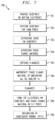
- FIGS. 1 - 6 illustrate a method for manufacturing a PCM device according to one or more embodiments of the present invention.
- FIG. 7 is a flow diagram of a method for manufacturing a PCM device according to one or more embodiments of the present invention.
- Phase-Change Memory is based on a chalcogenide glass material, which changes its phase from crystalline to amorphous and back again when suitable electrical currents are applied.
- GST alloy germanium-antimony-tellurium or Ge 2 Sb 2 Te 5
- Each phase has a differing resistance level, which is stable until the phase is changed.
- the maximum and minimum resistance levels in a PCM device are the basis for binary one or zero values.
- Embodiments of the present invention include methods for amorphization of a GST film using an implant process prior to CMP planarization.
- Ge, Sb or Te implants are used to amorphizatize the GST film, without substantially changing (e.g., less than 1% material) the composition of the GST.
- Embodiments of the present invention achieve good contact between the GST and a top electrode metal (not show) and exhibit no delamination defects.
- a confined cell 101 is formed with a void-free fill of phase-change material 102 (see FIG. 1 ).
- Embodiments of the present invention achieve good interfacial contact between the phase-change material 102 and a top electrode 103 .
- a first portion of the phase-change material 104 e.g., near the top electrode
- a second portion 105 is crystalline (e.g., near a bottom electrode).
- confined cell refers to a general category of PCM cell, and can be compared with contact minimized PCM cells.
- a current flow is most confined in the phase-change material (e.g., the phase-change material has a smallest cross-sectional area with respect to current flow).
- an electrode that connects to the phase-change material has a smallest cross-sectional area through which the current flows (e.g., the current is most confined by the contact to the phase change material).
- a method of manufacturing a PCM device is described with reference to FIGS. 2 - 7 and comprises providing a substrate 201 (e.g., an interlayer dielectric (ILD)) patterned to include a plurality of pores (e.g., pore 202 ) formed therein.
- a liner 203 is formed on the substrate 201 .
- the pores extend through the substrate 201 and to a bottom electrode 204 disposed below the substrate 201 .
- the substrate is patterned to have pores corresponding to the locations of a plurality of bottom electrodes, and that the bottom electrodes can be formed by depositing a bottom electrode metal on a lower surface of the substrate and patterning the bottom electrode metal.
- the substrate is formed of silicon nitride (SiN).
- the bottom electrode 204 can be formed of, for example, a metal or metal nitride.
- the liner 203 is a metallic liner formed by a CVD or ALD process.
- the liner can be formed of, for example, titanium nitride (TiN), titanium carbide (TiC), tungsten carbide (WC), tungsten nitride (WN), carbon (C), nitridohafnium (HfN), hafnium carbide (HfC), vanadium nitride (VN), vanadium carbides (VC), tantalum nitride (TaN), tantalum carbide (TaC), titanium silicon nitride (TiSiN), titanium aluminum nitride (TiAlN), tantalum silicon nitride (TaSiN), tantalum aluminum nitride (TaAlN), other carbides or nitrides of transition, refractory metals, etc.
- TiN titanium nitride
- TiC titanium carbide
- WC tungsten carbide
- WN tungsten nitride
- carbon C
- a phase-change material 301 such as a crystalline (poly-crystalline) or nano-crystalline GST film is deposited over the substrate 201 and liner 203 using a CVD/ALD process as shown in FIG. 3 .
- the phase change material 301 is deposited in a poly-crystalline state, avoiding shrinkage/density change associated with a phase transition associated with depositing the phase change material in an amorphous state and later crystallization, which can result in voids forming within the material.
- the phase-change material 301 is deposited by a Physical Vapor Deposition (PVD) process or a combination of CVD/ALD and PVD processes.
- PVD Physical Vapor Deposition
- the phase-change material 301 can be a single element (such as Sb only) or binary compounds GeTe or SbTe, with various stoichiometries, or a ternary alloy comprising of Ge, Te and Sb. Additionally, the phase change materials can be doped or intermixed with less than about 20% of nitrogen (N), carbon (C), oxygen (O), silicon (Si) or selenium (Se), or alloys containing these elements.
- a Ge, Sb or Te beam line implantation 401 is used to amorphize an overburden film 402 (i.e., a portion above the substrate 201 and liner 203 ) and at least a portion 403 of the phase-change material 301 inside the pore.
- an overburden film 402 i.e., a portion above the substrate 201 and liner 203
- the whole of the phase-change material 301 inside the pore is amorphized.
- the implants (based on the film/compound) can be used for amorphization of the phase-change material, without changing the composition of the phase-change material.
- the implantation dose of the Ge, Sb and/or Te is less than about 5 ⁇ 10 15 cm ⁇ 2 .
- the implantation 401 is performed at low temperatures (e.g., cold chuck, ⁇ 20 degrees Celsius) to create a sharp amorphous/crystalline boundary.
- an implanter current of ions (ion flux) is controlled such that excessive self-heating does not take place, and re-crystallization is avoided.
- the increase in temperature due to the ion implantation can be maintained below the crystallization temperature of the phase-change material (e.g., below about 165 degrees Celsius for GST225). Accordingly, one of ordinary skill in the art would understand how to achieve a dose needed to amorphized the GST.
- Ge, Sb, and/or Te is used during the implantation 401 to avoid introducing impurities other than atoms already in the GST alloy.
- other elements can be implanted for the purpose of the amorphization.
- Xe (54) can be used, which is a noble gas to obtain a substantially similar amorphization effect as Te (52).
- the ion implantation 401 can have the effect of changing poly-crystalline material into an amorphous material, without substantially modifying the overall composition of the material.
- the device 500 is planarized as shown in FIG. 5 , e.g., by a CMP, to remove the overburden film 402 and a top portion of the liner 203 .
- some dopant atoms will be implanted the dielectric layer in the case of the planar implants.
- the dose within the dielectric layer does not change the stoichiometry of the dielectric material.
- a first CMP process is performed to partially remove the overburden film 402 , followed by the implantation 401 , and a second CMP process to fully planarize the structure (e.g., remove an upper portion of the liner 203 on the substrate 201 ).
- the CMP process is performed on the phase change material in the amorphous phase, which substantially avoids the CMP pull out or break off crystalline chunks, which can remove phase-change material from the top of the pore.
- the phase change material is deposited in a poly-crystalline form and amorphized prior to the CMP process.
- subsequent processes have a high temperature budget, where the phase change material ends up poly-crystalline by the time the wafer processing is complete.
- a top electrode 601 is deposited over the pore, in contact with the phase-change material 301 (see FIG. 6 ). According to one or more embodiments, the top electrode 601 is patterned following deposition, and downstream integration of subsequent wiring levels (not shown) is performed.
- phase change material undergoes phase transformations, which changes the electrical resistance of the phase change memory cell.
- a plurality of the PCM devices are arranged as a 3-D crossbar array.
- each PCM device in the array is connected to a selector device, such as an ovonic threshold switch or a select transistor.
- a method for manufacturing a PCM device 700 comprises providing a substrate, such as an interlayer dielectric (ILD), on a plurality of bottom electrodes 701 , and patterning the substrate 702 to form a plurality of pores or vias therein extending from a surface of the substrate to the bottom electrodes.
- the method further comprises depositing a liner on the surface of the substrate 703 .
- Block 703 can further include etching the liner (such as by a reactive ion etch).
- the method includes depositing a phase-change material 704 , such as a crystalline or nano-crystalline GST film, over the substrate and liner.
- block 704 includes an anneal to densify the deposited phase-change material.
- the method further comprises implanting one or more of a Ge, Sb or Te in the phase-change material 706 to amorphize at least a portion of the phase-change material inside the pore.
- the method further comprises planarizing the device 707 to expose the surface of the substrate, removing the overburden film and a top portion of the liner.
- a first CMP process 705 performed to partially remove the overburden film, followed by the implantation 706 , and a second CMP process 707 to fully planarize the structure, removing an upper portion of the liner on the substrate.
- top electrodes are formed 708 by depositing a top electrode metal over the pores, in contact with the phase-change material, and patterning the top electrode metal. According to at least one embodiments, downstream integration of subsequent wiring levels (not shown) is performed 709 .
- the method further includes a wet clean between the amorphization 706 and the planarization 707 .
- a method for manufacturing a phase-change memory device 700 includes providing a substrate including a plurality of bottom electrodes 701 , patterning the substrate to form a plurality of pores in the substrate extending from a surface of the substrate to the bottom electrodes 702 , depositing a phase-change material over the substrate 704 , implanting one or more of a Ge, Sb and Te in the phase-change material to amorphize at least a portion of the phase-change material inside the pore 706 , planarizing the device to exposed the surface of the substrate 707 , and forming a plurality of top electrodes over the pores, in contact with the phase-change material 708 .
- a method for manufacturing a phase-change memory device 700 includes providing a substrate including a plurality of bottom electrodes 701 , patterning the substrate to form a plurality of pores in the substrate extending from a surface of the substrate to the bottom electrodes 702 , depositing a phase-change material over the substrate 704 , planarizing the device to exposed the surface of the substrate 705 , implanting one or more of a Ge, Sb and Te in the phase-change material to amorphize at least a portion of the phase-change material inside the pore 706 , planarizing the device to exposed the surface of the substrate 707 , and forming a plurality of top electrodes over the pores, in contact with the phase-change material 708 .
- a phase-change memory device includes a bottom electrode 204 , a substrate 201 formed on the bottom electrode, a pore 202 formed in the substrate extending to the bottom electrode, a phase-change material 301 disposed in the pore and comprising an amorphous portion 104 disposed in contact with a top electrode and a crystalline portion 105 disposed below the amorphous portion, wherein the amorphous portion comprises implanted ions, and a top electrode 601 disposed over the substrate in contact with the amorphous portion of the phase-change material, wherein the interface between the phase-change material and the top electrode is without voids.
- each block in the flowchart or block diagrams may represent a module, segment, or portion of instructions, which comprises one or more executable instructions for implementing the specified logical function(s).
- the functions noted in the blocks may occur out of the order noted in the Figures.
- two blocks shown in succession may, in fact, be executed substantially concurrently, or the blocks may sometimes be executed in the reverse order, depending upon the functionality involved.
Landscapes
- Engineering & Computer Science (AREA)
- Manufacturing & Machinery (AREA)
- Semiconductor Memories (AREA)
Abstract
Description
Claims (16)
Priority Applications (6)
| Application Number | Priority Date | Filing Date | Title |
|---|---|---|---|
| US17/086,658 US12004434B2 (en) | 2020-11-02 | 2020-11-02 | Fill-in confined cell PCM devices |
| GB2308092.2A GB2615957B (en) | 2020-11-02 | 2021-10-25 | Improved fill-in confined cell PCM devices |
| CN202180069014.7A CN116325094A (en) | 2020-11-02 | 2021-10-25 | Improved Packing Constrained Cell PCM Devices |
| JP2023522554A JP7663303B2 (en) | 2020-11-02 | 2021-10-25 | Improved filled confined cell PCM device |
| PCT/CN2021/126064 WO2022089359A1 (en) | 2020-11-02 | 2021-10-25 | Improved fill-in confined cell pcm devices |
| DE112021005780.4T DE112021005780B4 (en) | 2020-11-02 | 2021-10-25 | Method for producing an improved fill-in PCM unit with confined cells and PCM unit |
Applications Claiming Priority (1)
| Application Number | Priority Date | Filing Date | Title |
|---|---|---|---|
| US17/086,658 US12004434B2 (en) | 2020-11-02 | 2020-11-02 | Fill-in confined cell PCM devices |
Publications (2)
| Publication Number | Publication Date |
|---|---|
| US20220140237A1 US20220140237A1 (en) | 2022-05-05 |
| US12004434B2 true US12004434B2 (en) | 2024-06-04 |
Family
ID=81380487
Family Applications (1)
| Application Number | Title | Priority Date | Filing Date |
|---|---|---|---|
| US17/086,658 Active 2041-03-16 US12004434B2 (en) | 2020-11-02 | 2020-11-02 | Fill-in confined cell PCM devices |
Country Status (6)
| Country | Link |
|---|---|
| US (1) | US12004434B2 (en) |
| JP (1) | JP7663303B2 (en) |
| CN (1) | CN116325094A (en) |
| DE (1) | DE112021005780B4 (en) |
| GB (1) | GB2615957B (en) |
| WO (1) | WO2022089359A1 (en) |
Citations (9)
| Publication number | Priority date | Publication date | Assignee | Title |
|---|---|---|---|---|
| KR20060101950A (en) * | 2005-03-22 | 2006-09-27 | 한국표준과학연구원 | Memory and its manufacturing method |
| US20070160760A1 (en) * | 2006-01-10 | 2007-07-12 | Samsung Electronics Co., Ltd. | Methods of forming phase change material thin films and methods of manufacturing phase change memory devices using the same |
| US20070267620A1 (en) | 2006-05-18 | 2007-11-22 | Thomas Happ | Memory cell including doped phase change material |
| US20090227087A1 (en) * | 2008-03-04 | 2009-09-10 | Varian Semiconductor Equipment Associates, Inc. | Method to improve uniformity of chemical mechanical polishing planarization |
| US20110001107A1 (en) * | 2009-07-02 | 2011-01-06 | Advanced Technology Materials, Inc. | Hollow gst structure with dielectric fill |
| US20130078475A1 (en) | 2010-03-26 | 2013-03-28 | Advanced Technology Materials, Inc. | Germanium antimony telluride materials and devices incorporating same |
| WO2013152088A1 (en) | 2012-04-04 | 2013-10-10 | Advanced Technology Materials, Inc. | Gst deposition process |
| US8618524B2 (en) | 2007-09-20 | 2013-12-31 | Taiwan Semiconductor Manufacturing Company, Ltd. | Phase change memory with various grain sizes |
| US20190325954A1 (en) | 2018-04-20 | 2019-10-24 | International Business Machines Corporation | Bipolar switching operation of confined phase change memory for a multi-level cell memory |
Family Cites Families (5)
| Publication number | Priority date | Publication date | Assignee | Title |
|---|---|---|---|---|
| US6159874A (en) * | 1999-10-27 | 2000-12-12 | Infineon Technologies North America Corp. | Method of forming a hemispherical grained capacitor |
| TW507365B (en) * | 2001-03-09 | 2002-10-21 | Nanya Technology Corp | Method for treating surface of sidewall of deep trench |
| JP2006202823A (en) * | 2005-01-18 | 2006-08-03 | Renesas Technology Corp | Semiconductor memory device and its manufacturing method |
| US20090230375A1 (en) * | 2008-03-17 | 2009-09-17 | Taiwan Semiconductor Manufacturing Company, Ltd. | Phase Change Memory Device |
| US10770656B2 (en) * | 2018-09-20 | 2020-09-08 | International Business Machines Corporation | Method for manufacturing phase change memory |
-
2020
- 2020-11-02 US US17/086,658 patent/US12004434B2/en active Active
-
2021
- 2021-10-25 DE DE112021005780.4T patent/DE112021005780B4/en active Active
- 2021-10-25 CN CN202180069014.7A patent/CN116325094A/en active Pending
- 2021-10-25 GB GB2308092.2A patent/GB2615957B/en active Active
- 2021-10-25 WO PCT/CN2021/126064 patent/WO2022089359A1/en not_active Ceased
- 2021-10-25 JP JP2023522554A patent/JP7663303B2/en active Active
Patent Citations (10)
| Publication number | Priority date | Publication date | Assignee | Title |
|---|---|---|---|---|
| KR20060101950A (en) * | 2005-03-22 | 2006-09-27 | 한국표준과학연구원 | Memory and its manufacturing method |
| US20070160760A1 (en) * | 2006-01-10 | 2007-07-12 | Samsung Electronics Co., Ltd. | Methods of forming phase change material thin films and methods of manufacturing phase change memory devices using the same |
| US20070267620A1 (en) | 2006-05-18 | 2007-11-22 | Thomas Happ | Memory cell including doped phase change material |
| US8618524B2 (en) | 2007-09-20 | 2013-12-31 | Taiwan Semiconductor Manufacturing Company, Ltd. | Phase change memory with various grain sizes |
| US20090227087A1 (en) * | 2008-03-04 | 2009-09-10 | Varian Semiconductor Equipment Associates, Inc. | Method to improve uniformity of chemical mechanical polishing planarization |
| US20110001107A1 (en) * | 2009-07-02 | 2011-01-06 | Advanced Technology Materials, Inc. | Hollow gst structure with dielectric fill |
| US8410468B2 (en) | 2009-07-02 | 2013-04-02 | Advanced Technology Materials, Inc. | Hollow GST structure with dielectric fill |
| US20130078475A1 (en) | 2010-03-26 | 2013-03-28 | Advanced Technology Materials, Inc. | Germanium antimony telluride materials and devices incorporating same |
| WO2013152088A1 (en) | 2012-04-04 | 2013-10-10 | Advanced Technology Materials, Inc. | Gst deposition process |
| US20190325954A1 (en) | 2018-04-20 | 2019-10-24 | International Business Machines Corporation | Bipolar switching operation of confined phase change memory for a multi-level cell memory |
Non-Patent Citations (5)
| Title |
|---|
| Authorized Officer Wang,Xiaofeng, PRC National IP Administration as ISA, related PCT application PCT/CN2021/126064, ISR and Written Opinion, 9 pages total, dated Jan. 29, 2022. |
| English translation of Kim Young Kuk et al (KR 20060101950 A), Memory and Manufacturing Method Thereof (Year: 2006). * |
| Ralph Schneider, German Patent and Trademark Office, Office Action and Examination Notice in related German application 11 2021 005 780.4, 7 pages total, mailed Mar. 17, 2024 (English Translation of Original German Document). |
| Raoux et al., "Amorphization of Crystalline Phase Change Material by Ion Implantation" 2010 MRS Spring Meeting, Apr. 2010, pp. 1-7. |
| Wong et al., "Phase Change Memory" Proceedings of the IEEE, vol. 98, No. 12, Dec. 2010, pp. 1-27. |
Also Published As
| Publication number | Publication date |
|---|---|
| GB202308092D0 (en) | 2023-07-12 |
| GB2615957B (en) | 2025-09-10 |
| GB2615957A (en) | 2023-08-23 |
| US20220140237A1 (en) | 2022-05-05 |
| WO2022089359A1 (en) | 2022-05-05 |
| DE112021005780T5 (en) | 2023-09-21 |
| JP7663303B2 (en) | 2025-04-16 |
| DE112021005780B4 (en) | 2025-10-02 |
| JP2023547355A (en) | 2023-11-10 |
| CN116325094A (en) | 2023-06-23 |
Similar Documents
| Publication | Publication Date | Title |
|---|---|---|
| US9190610B2 (en) | Methods of forming phase change memory with various grain sizes | |
| TWI469268B (en) | Method for forming a memory cell using a gas cluster ion beam | |
| US8030634B2 (en) | Memory array with diode driver and method for fabricating the same | |
| US7879645B2 (en) | Fill-in etching free pore device | |
| US20080210923A1 (en) | Semiconductor device and method of manufacturing the same | |
| US11271151B2 (en) | Phase change memory using multiple phase change layers and multiple heat conductors | |
| US11805714B2 (en) | Phase change memory with conductive bridge filament | |
| US20090029031A1 (en) | Methods for forming electrodes in phase change memory devices | |
| TWI879813B (en) | Titanium silicon nitride barrier layer | |
| TW200849685A (en) | Methods of forming a phase-change material layer including tellurium and methods of manufacturing a phase-change memory device using the same | |
| KR20080095683A (en) | Phase change memory device and method of forming the same | |
| US11430954B2 (en) | Resistance drift mitigation in non-volatile memory cell | |
| US10833269B1 (en) | 3D phase change memory | |
| US11957069B2 (en) | Contact resistance of a metal liner in a phase change memory cell | |
| US20120009731A1 (en) | Method of manufacturing phase-change random access memory | |
| US12004434B2 (en) | Fill-in confined cell PCM devices | |
| CN113130743A (en) | storage unit | |
| US8716060B2 (en) | Confined resistance variable memory cell structures and methods | |
| KR102933806B1 (en) | titanium silicon nitride barrier layer | |
| KR20210050026A (en) | Variable resistance memory device and method of forming the same |
Legal Events
| Date | Code | Title | Description |
|---|---|---|---|
| AS | Assignment |
Owner name: INTERNATIONAL BUSINESS MACHINES CORPORATION, NEW YORK Free format text: ASSIGNMENT OF ASSIGNORS INTEREST;ASSIGNORS:ADUSUMILLI, PRANEET;BRIGHTSKY, MATTHEW JOSEPH;COHEN, GUY M.;AND OTHERS;SIGNING DATES FROM 20201028 TO 20201101;REEL/FRAME:054239/0949 |
|
| FEPP | Fee payment procedure |
Free format text: ENTITY STATUS SET TO UNDISCOUNTED (ORIGINAL EVENT CODE: BIG.); ENTITY STATUS OF PATENT OWNER: LARGE ENTITY |
|
| STPP | Information on status: patent application and granting procedure in general |
Free format text: DOCKETED NEW CASE - READY FOR EXAMINATION |
|
| STPP | Information on status: patent application and granting procedure in general |
Free format text: NON FINAL ACTION MAILED |
|
| STPP | Information on status: patent application and granting procedure in general |
Free format text: RESPONSE TO NON-FINAL OFFICE ACTION ENTERED AND FORWARDED TO EXAMINER |
|
| STPP | Information on status: patent application and granting procedure in general |
Free format text: NON FINAL ACTION MAILED |
|
| STPP | Information on status: patent application and granting procedure in general |
Free format text: FINAL REJECTION MAILED |
|
| STPP | Information on status: patent application and granting procedure in general |
Free format text: DOCKETED NEW CASE - READY FOR EXAMINATION |
|
| STPP | Information on status: patent application and granting procedure in general |
Free format text: NOTICE OF ALLOWANCE MAILED -- APPLICATION RECEIVED IN OFFICE OF PUBLICATIONS |
|
| STPP | Information on status: patent application and granting procedure in general |
Free format text: NOTICE OF ALLOWANCE MAILED -- APPLICATION RECEIVED IN OFFICE OF PUBLICATIONS |
|
| STPP | Information on status: patent application and granting procedure in general |
Free format text: PUBLICATIONS -- ISSUE FEE PAYMENT VERIFIED |
|
| STCF | Information on status: patent grant |
Free format text: PATENTED CASE |