US12003236B2 - Semiconductor device - Google Patents
Semiconductor device Download PDFInfo
- Publication number
- US12003236B2 US12003236B2 US17/688,482 US202217688482A US12003236B2 US 12003236 B2 US12003236 B2 US 12003236B2 US 202217688482 A US202217688482 A US 202217688482A US 12003236 B2 US12003236 B2 US 12003236B2
- Authority
- US
- United States
- Prior art keywords
- gate
- source
- drain
- potential
- transistor
- Prior art date
- Legal status (The legal status is an assumption and is not a legal conclusion. Google has not performed a legal analysis and makes no representation as to the accuracy of the status listed.)
- Active, expires
Links
Images


Classifications
-
- H—ELECTRICITY
- H03—ELECTRONIC CIRCUITRY
- H03K—PULSE TECHNIQUE
- H03K19/00—Logic circuits, i.e. having at least two inputs acting on one output; Inverting circuits
- H03K19/003—Modifications for increasing the reliability for protection
- H03K19/0033—Radiation hardening
- H03K19/00338—In field effect transistor circuits
-
- H—ELECTRICITY
- H03—ELECTRONIC CIRCUITRY
- H03K—PULSE TECHNIQUE
- H03K19/00—Logic circuits, i.e. having at least two inputs acting on one output; Inverting circuits
- H03K19/0175—Coupling arrangements; Interface arrangements
- H03K19/0185—Coupling arrangements; Interface arrangements using field effect transistors only
- H03K19/018507—Interface arrangements
- H03K19/018521—Interface arrangements of complementary type, e.g. CMOS
Definitions
- Embodiments relate to a semiconductor device.
- a semiconductor device includes a semiconductor device having a field-effect transistor (FET).
- FET field-effect transistor
- FIG. 1 is a block diagram illustrating a configuration example of a semiconductor device.
- FIG. 2 is a schematic circuit diagram illustrating a first configuration example of an electronic circuit 1 .
- FIG. 3 is a cross-sectional schematic view illustrating a structure example of a field-effect transistor.
- FIG. 4 is a schematic sectional view illustrating a structure example of the transistor.
- FIG. 5 is a timing chart for explaining a first operation example of a first configuration example of a semiconductor device 10 .
- FIG. 6 is a schematic circuit diagram for explaining the operation in a period P 1 .
- FIG. 7 is a schematic circuit diagram for explaining the operation in a period P 2 .
- FIG. 8 is a schematic circuit diagram for explaining the operation in a period P 3 .
- FIG. 9 is a timing chart for explaining a second operation example of the first configuration example of the electronic circuit 1 .
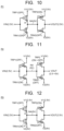
- FIG. 10 is a schematic circuit diagram for explaining the operation in the period P 1 .
- FIG. 11 is a schematic circuit diagram for explaining the operation in the period P 2 .
- FIG. 12 is a schematic circuit diagram for explaining the operation in the period P 3 .
- FIG. 13 is a schematic circuit diagram illustrating a second configuration example of the electronic circuit 1 .
- FIG. 14 is a timing chart for explaining a first operation example of a second configuration example of the device 10 .
- FIG. 15 is a schematic circuit diagram for explaining the operation in the period P 1 .
- FIG. 16 is a schematic circuit diagram for explaining the operation in the period P 2 .
- FIG. 17 is a schematic circuit diagram for explaining the operation in the period P 3 .
- FIG. 18 is a timing chart for explaining a second operation example of a second configuration example of the electronic circuit 1 .
- FIG. 19 is a schematic circuit diagram for explaining the operation in the period P 1 .
- FIG. 20 is a schematic circuit diagram for explaining the operation in the period P 2 .
- FIG. 21 is a schematic circuit diagram for explaining the operation in the period P 3 .
- FIG. 22 is a schematic circuit diagram illustrating a third configuration example of the electronic circuit 1 .
- FIG. 23 is a timing chart for explaining a first operation example of a third configuration example of the device 10 .
- FIG. 24 is a schematic circuit diagram for explaining the operation in the period P 1 .
- FIG. 25 is a schematic circuit diagram for explaining the operation in the period P 2 .
- FIG. 26 is a schematic circuit diagram for explaining the operation in the period P 3 .
- FIG. 27 is a timing chart for explaining a second operation example of a third configuration example of the electronic circuit 1 .
- FIG. 28 is a schematic circuit diagram for explaining the operation in the period P 1 .
- FIG. 29 is a schematic circuit diagram for explaining the operation in the period P 2 .
- FIG. 30 is a schematic circuit diagram for explaining the operation in the period P 3 .
- FIG. 31 is a schematic circuit diagram illustrating another configuration example of a semiconductor device.
- FIG. 32 is a schematic circuit diagram illustrating the other configuration example of the device.
- FIG. 33 is a schematic circuit diagram illustrating the other configuration example of the device.
- a semiconductor device in an embodiment includes: an electronic circuit configured to receive a first signal and transmit a second signal; a power supply circuit configured to supply a power supply voltage to the electronic circuit; and a correction circuit configured to control the power supply circuit to change a value of the power supply voltage to switch between a normal operation mode and a refresh operation mode of the device.
- the electronic circuit comprises: a first P-channel type field-effect transistor having a first gate, a first source, and a first drain, a potential of the first gate changing in response to the first signal, and a potential of one of the first source and the first drain changing in response to the power supply voltage; and a first N-channel type field-effect transistor having a second gate, a second source, and a second drain, the second gate being electrically connected to the first gate, a potential of one of the second source and the second drain being equal to or lower than a ground potential, and another of the second source and the second drain being electrically connected to another of the first source and the first drain.
- the refresh operation mode comprises at least one operation selected from the group consisting of: a first operation of applying a negative voltage between the first gate and at least one selected from the group consisting of the first source and the first drain so that the first gate is lower in potential than the at least one selected from the group consisting of the first source and the first drain, and applying a negative voltage between the second gate and at least one selected from the group consisting of the second source and the second drain so that the second gate is lower in potential than the at least one selected from the group consisting of the second source and the second drain; a second operation of applying a positive voltage between the first gate and at least one selected from the group consisting of the first source and the first drain so that the first gate is higher in potential than the at least one selected from the group consisting of the first source and the first drain, and applying a positive voltage between the second gate and at least one selected from the group consisting of the second source and the second drain so that the second gate is higher in potential than the at least one selected from the group consisting of the second source and the second drain; and
- FIG. 1 is a block diagram illustrating a configuration example of a semiconductor device.
- a semiconductor device 10 includes an electronic circuit 1 , a power supply circuit 2 , and a correction circuit 3 .
- the electronic circuit 1 is a circuit to be controlled.
- the electronic circuit 1 has a function of receiving a signal IN and transmits a signal OUT.
- the electronic circuit 1 may have a NOT gate (also referred to as a NOT circuit, an inverter circuit), a NOR gate (also referred to as a NOR circuit), or a NAND gate (also referred to as a NAND circuit).
- the electronic circuit 1 may have, but not limited to these logic gates, another logic gate.
- the power supply circuit 2 has a function of supplying a power supply voltage VDD to the electronic circuit 1 .
- the power supply circuit 2 can change the value of the power supply voltage VDD to be supplied to the electronic circuit 1 in response to a signal from the correction circuit 3 .
- An example of the power supply has a plurality of switches and switches ON/OFF of each of the switches in response to the signal from the correction circuit 3 , and thus can change the value of the power supply voltage VDD.
- the correction circuit 3 receives the signal IN and the signal OUT.
- the correction circuit 3 has a function of controlling the power supply circuit 2 referring to the signal IN as needed according to the fluctuation of the signal OUT to change the value of the power supply voltage VDD, thereby switching among a plurality of operation modes of the device 10 .
- An example of the correction circuit 3 transmits a signal to the power supply circuit 2 , the signal being for commanding the power supply circuit 2 to change the value of the power supply voltage VDD to be output from the power supply circuit 2 .
- FIG. 2 is a schematic circuit diagram illustrating a first configuration example of the electronic circuit 1 .
- the electronic circuit 1 has a transistor TRP 1 , a transistor TRN 1 , a transistor TRP 2 , and a transistor TRN 2 .
- the transistors TRP 1 and TRP 2 are P-channel type field-effect transistors.
- the transistors TRN 1 and TRN 2 are N-channel type field-effect transistors.
- the transistors TRP 1 and TRN 1 form a first NOT gate.
- the transistors TRP 2 and TRN 2 form a second NOT gate. Examples of the electronic circuit 1 having the NOT gates include a level shift circuit.
- the transistor has a gate, a source, and a drain.
- the transistor may further have a back gate.
- the source and the drain are replaced with each other in response to the structure and the operation condition of the transistor, and therefore it is difficult to limit which of them is the source or the drain.
- one terminal arbitrarily selected from the source and the drain is indicated as one of the source and the drain, and the other terminal is indicated as the other of the source and the drain unless otherwise stated.
- the transistor TRP 1 has a first gate, a first source, and a first drain.
- the first gate has a potential VIN changing in response to the signal IN.
- One of the first source and the first drain has a potential V 1 changing in response to the power supply voltage VDD.
- the transistor TRN 1 has a second gate, a second source, and a second drain.
- the second gate is electrically connected to the first gate.
- One of the second source and the second drain has a potential V 2 being equal to or lower than the ground potential in their values.
- the other of the second source and the second drain is electrically connected to the other of the first source and the first drain to form a node NA therebetween.
- the transistor TRP 2 has a third gate, a third source, and a third drain.
- the third gate is electrically connected to the node NA.
- One of the third source and the third drain has the potential V 1 .
- the transistor TRN 2 has a fourth gate, a fourth source, and a fourth drain.
- the fourth gate is electrically connected to the third gate.
- One of the fourth source and the fourth drain has the potential V 2 .
- the other of the fourth source and the fourth drain is electrically connected to the other of the third source and the third drain and has a potential VOUT of the signal OUT.
- FIG. 3 is a cross-sectional schematic view illustrating a structure example of the transistor.
- a semiconductor substrate 200 on which an N-channel type field-effect transistor TR N and a P-channel type field-effect transistor TR P are to be formed has a surface 200 a and a surface 200 b .
- FIG. 3 further illustrates a semiconductor region 201 , a p-type well region (Pwell) 202 p , an n-type well region (Nwell) 202 n , and an element isolator 207 which are formed in the semiconductor substrate 200 .
- Pwell p-type well region
- Nwell n-type well region
- the semiconductor region 201 is a substrate region of the semiconductor substrate 200 and provided between the surface 200 a and the surface 200 b .
- An example of the surface 200 a and the surface 200 b extend in an X-axis direction and a Y-axis direction.
- An example of a thickness direction of the semiconductor substrate 200 is Z-axis direction.
- One of the surface 200 a and the surface 200 b is provided on the side opposite to the other of the surface 200 a and the surface 200 b.
- the semiconductor region 201 may contain silicon (Si).
- the semiconductor region 201 may contain an acceptor impurity such as boron (B).
- the p-type well region 202 p is provided on the surface 200 a .
- the p-type well region 202 p contains an acceptor impurity such as boron (B).
- the p-type well region 202 p is higher in acceptor concentration than the semiconductor region 201 .
- the n-type well region 202 n is provided on the surface 200 a .
- the n-type well region 202 n may contain a donor impurity such as phosphor (P) or arsenic (As).
- the n-type well region 202 n is higher in donor concentration than the semiconductor region 201 .
- the element isolator 207 is provided between the transistor TR N and the transistor TR P to isolate the transistor TR N and the transistor TR P from each other.
- the element isolator 207 may contain silicon oxide.
- the transistor TR N includes impurity regions 208 a , a gate insulating film 209 a , a gate electrode 210 a , an insulating film 211 a , and an insulating layer 212 a .
- the transistor TR P includes impurity regions 208 b , a gate insulating film 209 b , a gate electrode 210 b , an insulating film 211 b , and an insulating layer 212 b.
- the impurity regions 208 a are provided in the p-type well region 202 p .
- the impurity regions 208 a each form a source region or a drain region of the transistor TR N .
- the transistor TR N has a channel region between the impurity regions 208 a .
- the impurity regions 208 a contain may the donor impurity.
- Each impurity region 208 a is connected to one of contact plugs 213 a.
- the impurity regions 208 b are provided in the n-type well region 202 n .
- the impurity regions 208 b each form a source region or a drain region of the transistor TR P .
- the transistor TR P has a channel region between the impurity regions 208 b .
- the impurity regions 208 b may contain the acceptor impurity.
- Each impurity region 208 b is connected to one of contact plugs 213 b.
- the gate insulating film 209 a is provided above the p-type well region 202 p .
- the gate insulating film 209 b is provided above the n-type well region 202 n .
- Each of the gate insulating films 209 a and 209 b may contain a silicon oxide film.
- the gate electrode 210 a is provided above the gate insulating film 209 a .
- the gate electrode 210 b is provided above the gate insulating film 209 b .
- Each of the gate electrodes 210 a and 210 b may contain a conductive layer such as a polysilicon layer containing doped carbon, a polysilicon layer containing doped phosphor, a titanium layer, a metal nitride layer containing titanium nitride or tungsten nitride, or a tungsten layer. These conductive layers may be stacked in order to form the gate electrodes 210 a and 210 b .
- the gate electrode 210 a is connected to one of the contact plugs 213 a .
- the gate electrode 210 b is connected to one of the contact plugs 213 b.
- the insulating film 211 a is provided above the gate electrode 210 a .
- the insulating film 211 b is provided above the gate electrode 210 b .
- the insulating films 211 a and 211 b may function as etching stoppers when forming contact plugs to the gate electrodes 210 a and 210 b .
- Examples of each of the insulating films 211 a and 211 b include a silicon nitride (SiN) film.
- Each of the insulating layers 212 a and 212 b may include a first insulating layer and a second insulating layer provided on the first insulating layer.
- the first and second insulating layers are provided on a side surface of a stack of the gate electrode 210 a and the insulating film 211 a and a side surface of a stack of the gate electrode 210 b and the insulating film 211 b , respectively, and extend along a thickness direction of the stacks.
- Examples of the first insulating layer include a silicon dioxide (SiO 2 ) layer.
- Examples of the second insulating layer include a silicon nitride (SiN) layer.
- the insulating layers 212 a and 212 b may function as side walls of the transistors TR N and TR P , respectively.
- Radiation exposure of a field-effect transistor such as the transistors TR N or TR P may shift its threshold voltage or decrease its ON current. Such deterioration causes an operation failure of the device 10 .
- the transistors in the device 10 are exposed to a radiation ray.
- the transistors may be exposed to a radiation ray inside the device 10 of the radiation inspection device.
- FIG. 4 is a schematic sectional view illustrating a structure example of the transistor.
- FIG. 4 illustrates the transistor TR P as an example, and the same also applies to the transistor TR N .
- Radiation exposure of the transistor TR P may generate a positive fixed charge in the gate insulating film 209 b . This fixed charge may cause shift the threshold voltage.
- the radiation exposure of the transistor TR P may cause holes to break Si—H bonds at the interface between the channel region and the gate insulating film 209 b to form an interface state. Capture of electrons into the interface state may shift the threshold voltage and decrease the ON current.
- protons when the transistor TR P receives the radiation ray, protons (ft) may be generated.
- the protons may be generated not only in the gate insulating film 209 b and the insulating layer 212 b but also at some places such as the insulating region of the element isolator 207 about the transistor TR P .
- the protons generated about the transistor TR P enter an oxide film such as the gate insulating film 209 b of the transistor TR P . This shifts the threshold voltage.
- the device in the embodiment performs a refresh operation when the transistor is deteriorated due to the radiation ray.
- the refresh operation improves the shift of the threshold voltage and the decrease in the ON current of the transistor to reduce the operation failure of the device.
- the operation example of the device 10 includes a plurality of operations.
- the values of potentials and voltages are indicated by numerical values for convenience, and these values are set, for example, based on the specifications of the device 10 and not limited to the numerical values indicated below.
- FIG. 5 is a timing chart for explaining a first operation example of a first configuration example of the device 10 .
- the timing chart illustrated in FIG. 5 has a period P 0 , a period P 1 , a period P 2 , a period P 3 , and a period PX.
- the device 10 has a normal operation mode and a refresh operation mode. Each of the operation modes will be explained below.
- the normal operation mode causes the value of the power supply voltage VDD to be set to a value VA, the signal IN to be input into the first and second gates, and the signal OUT to be output.
- An example of the value VA is higher than the value of the ground potential, and is 1.5 V.
- An example of the potential VIN alternates between a value VH and a value VL to form pulses of the signal IN.
- An example of the value VL is equal to or lower than the value of the ground potential, and is 0 V.
- An example of the value VH is higher than the value of the ground potential, and is 1.5 V.
- An example of the potential VOUT alternates between the value VH and the value VL to form pulses of the signal OUT.
- the pulse waveforms of the signal IN and the signal OUT are not limited to the waveforms illustrated in FIG. 5 .
- the device 10 operates in the refresh operation mode.
- the value of the potential VIN is set to the value VL before a time T 1
- the value of the power supply voltage VDD changes from the value VA to a value VB at the time T 1 .
- An example of the value VB is higher than the value VA, and is 2.5 V.
- An example of the potential VIN can be set to the value VL by setting the potential of the signal IN to the electronic circuit 1 to the value VL.
- the time T 1 may be set to a refresh time set in advance, or may be set referring to the signal IN as needed according to the fluctuation of the signal OUT. Further, the potential of the signal IN may be changed to a value in accordance with each operation mode using a not-illustrated signal converter circuit.
- FIG. 6 is a schematic circuit diagram for explaining the operation in the period P 1 .
- the transistors TRP 1 and TRN 2 are turned into an on-state (ON), and the transistors TRN 1 and TRP 2 are turned into an off-state (OFF).
- the value of a potential VNA of the node NA changes from the value VH (1.5 V) to the value VB (2.5 V).
- a negative voltage is applied between the first gate and the first source of the transistor TRP 1 so that the first gate is lower in potential than the first source of the transistor TRP 1
- a negative voltage is applied between the second gate and the second drain of the transistor TRN 1 so that the second gate is lower in potential than the second drain of the transistor TRN 1 .
- This can draw the protons or holes caused by the radiation ray incident on the device 10 to remove them via each of the first and second gates.
- “a negative voltage between two terminals of a transistor” shows that the lower potential of the potentials of the two terminals is negative to the higher potential thereof.
- the operation of drawing the protons or holes via the gates in the above manner is also called a first refresh operation.
- a positive voltage is applied between the third gate and the third drain of the transistor TRP 2 so that the third gate is higher in potential than the third drain of the transistor TRP 2 , and a positive voltage is applied between the third drain and the third source of the transistor TRP 2 .
- This can draw the protons or holes caused by the radiation ray incident on the device 10 to the channel region via the gate insulating film of the transistor TRP 2 , the drawn protons or holes moving in the channel region to be removed from the channel region.
- a positive voltage between two terminals of a transistor shows that the higher potential of the potentials of the two terminals is positive to the lower potential thereof.
- the protons or holes drawn to the channel region may be moved into the semiconductor substrate 200 and drawn even without applying voltage thereto, and therefore it is not always necessary to move them in the channel region by applying the voltage between the drain and the source.
- Such an operation of removing the protons or holes via the channel region in the above manner is also called a second refresh operation.
- the value of the power supply voltage VDD to be supplied to the electronic circuit 1 changes from the value VB to a value VC at a time T 2 , and the value of the potential VIN is maintained at the value VL.
- An example of the value VC is lower than the value VA and equal to or lower than the ground potential, and is 0 V.
- FIG. 7 is a schematic circuit diagram for explaining the operation in the period P 2 .
- the transistors TRP 1 and TRN 2 are in the on-state, and therefore the value of the potential VNA transiently changes from the value VB (2.5 V) during which the transistors TRP 1 and TRN 2 are turned into the off-state, and is set to the value VL at a time TX. Further, in the period P 2 , the transistors TRN 1 and TRP 2 are maintained in the off-state (OFF).
- a negative voltage is applied between the first gate and the first drain of the transistor TRP 1 so that the first gate is lower in potential than the first drain of the transistor TRP 1
- a positive voltage is applied between the first drain and the first source of the transistor TRP 1
- a negative voltage is applied between the second gate and the second drain of the transistor TRN 1 so that the second gate is lower in potential than the second drain of the transistor TRN 1
- a positive voltage is applied between the second drain and the second source of the transistor TRN 1 .
- This can inject hot electrons into the gate insulating films of the transistors TRP 1 and TRN 1 via the channel regions. This can neutralize the protons or holes, which are caused by the radiation ray incident on the device 10 , in the gate insulating films.
- the operation of neutralizing the protons or holes by the hot electrons in this manner is also called a third refresh operation.
- a positive voltage is applied between the third gate and the third source of the transistor TRP 2 so that the third gate is higher in potential than the third source of the transistor TRP 2
- a positive voltage is applied between the fourth gate and the fourth source of the transistor TRN 2 so that the fourth gate is higher in potential than the fourth source of the transistor TRN 2 .
- the value of the power supply voltage VDD to be supplied to the electronic circuit 1 changes from the value VC (0 V) to the value VB (2.5 V) at a time T 3 , and the value of the potential VIN is maintained at the value VL (0 V).
- FIG. 8 is a schematic circuit diagram for explaining the operation in the period P 3 .
- the transistors TRP 1 and TRN 2 are turned into the on-state (ON), and the transistors TRN 1 and TRP 2 are turned into the off-state (OFF).
- the value of the potential VNA changes from the value VL (0 V) to the value VB (2.5 V).
- a negative voltage is applied between the first gate and the first source of the transistor TRP 1 so that the first gate is lower in potential than the first source of the transistor TRP 1
- a negative voltage is applied between the second gate and the second drain of the transistor TRN 1 so that the second gate is lower in potential than the second drain of the transistor TRN 1 .
- a positive voltage is applied between the third drain and the third source of the transistor TRP 2
- a positive voltage is applied between the fourth gate and the fourth source of the transistor TRN 2 . This can move the protons or holes caused by the radiation ray incident on the device 10 into the channel regions of the transistors TRP 2 and TRN 2 to remove the protons or holes.
- the protons or holes are drawn to the channel region via the gate insulating film in the transistor TRN 2 .
- the device 10 operates in the normal operation mode again after a time T 4 .
- the above is the explanation of the first operation example.
- FIG. 9 is a timing chart for explaining a second operation example of the first configuration example of the electronic circuit 1 .
- the second operation example of the first configuration example is different in the value of the potential VIN in the periods P 1 to P 3 as compared with the first operation example of the first configuration example.
- a portion of the second operation example different from that in the first operation example will be explained below, and the explanation of the first operation example can be appropriately employed for the other portion.
- the device 10 operates in the refresh operation mode.
- the value of the potential VIN is set to the value VB (2.5 V) before the time T 1
- the value of the power supply voltage VDD to be supplied to the electronic circuit 1 changes from the value VA (1.5 V) to the value VB (2.5 V) at the time T 1 .
- the time T 1 may be set to the same timing as the correction of the other electronic circuit, or may be set according to the time until the gate capacitance of the transistor connected to the potential VIN is charged.
- FIG. 10 is a schematic circuit diagram for explaining the operation in the period P 1 .
- the transistors TRP 1 and TRN 2 are turned into the off-state (OFF), and the transistors TRN 1 and TRP 2 are turned into the on-state (ON).
- the value of the potential VNA of the node NA is maintained at the value VL (0 V)
- the value of the potential of the signal OUT is maintained at the value VB (2.5 V).
- a negative voltage is applied between the third gate and the third source of the transistor TRP 2 so that the third gate is lower in potential than the third source of the transistor TRP 2
- a negative voltage is applied between the fourth gate and the fourth drain of the transistor TRN 2 so that the fourth gate is lower in potential than the fourth drain of the transistor TRN 2 .
- a positive voltage is applied between the first drain and the first source of the transistor TRP 1
- a positive voltage is applied between the second gate and the second source of the transistor TRN 1 so that the second gate is higher in potential than the second source of the transistor TRN 1 .
- This can move the protons or holes caused by the radiation ray incident on the device 10 into the channel regions of the transistors TRP 1 and TRN 1 to remove the protons or holes.
- the protons or holes are drawn to the channel region via the gate insulating film in the transistor TRN 1 .
- the value of the power supply voltage VDD to be supplied to the electronic circuit 1 changes from the value VB (2.5 V) to the value VC (0 V) at the time T 2 , and the value of the potential VIN is maintained at the value VX (2.5 V).
- FIG. 11 is a schematic circuit diagram for explaining the operation in the period P 2 .
- the transistors TRN 1 and TRP 2 are in the on-state (ON), and therefore the value of the potential VOUT of the signal OUT transiently changes from the value VB (2.5 V) during which the transistor TRP 2 is turned into the off-state, and is set to the value VL (0 V) at the time VX.
- the transistor TRN 1 is maintained in the on-state and the transistors TRP 1 and TRN 2 are maintained in the off-state (OFF).
- a negative voltage is applied between the third gate and the third drain of the transistor TRP 2 so that the third gate is lower in potential than the third drain of the transistor TRP 2
- a positive voltage is applied between the third drain and the third source of the transistor TRP 2
- a negative voltage is applied between the fourth gate and the fourth drain of the transistor TRN 2 so that the fourth gate is lower in potential than the fourth drain of the transistor TRN 2
- a positive voltage is applied between the fourth drain and the fourth source of the transistor TRN 2 at the time T 2 .
- This can inject hot electrons into the gate insulating films of the transistors TRP 2 and TRN 2 via the channel regions. This can neutralize the protons or holes, which are caused by the radiation ray incident on the device 10 , in the gate insulating films.
- a positive voltage is applied between the first gate and the first source of the transistor TRP 1 so that the first gate is higher in potential than the first source of the transistor TRP 1
- a positive voltage is applied between the second gate and the second source of the transistor TRN 1 so that the second gate is higher in potential than the second source of the transistor TRN 1 .
- the value of the power supply voltage VDD to be supplied to the electronic circuit 1 changes from the value VC (0 V) to the value VB (2.5 V) at the time T 3 , and the value of the potential VIN is maintained at the value VX (2.5 V).
- FIG. 12 is a schematic circuit diagram for explaining the operation in the period P 3 .
- the transistors TRP 1 and TRN 2 are turned into the off-state (OFF), and the transistors TRN 1 and TRP 2 are turned into the on-state (ON).
- the value of the potential VNA of the node NA is maintained at the value VL (0 V)
- the value of the potential VOUT of the signal OUT changes from the value VL (0 V) to the value VB (2.5 V).
- a negative voltage is applied between the third gate and the third source of the transistor TRP 2 so that the third gate is lower in potential than the third source of the transistor TRP 2
- a negative voltage is applied between the fourth gate and the fourth drain of the transistor TRN 2 so that the fourth gate is lower in potential than the fourth drain of the transistor TRN 2 .
- a positive voltage is applied between the first drain and the first source of the transistor TRP 1
- a positive voltage is applied between the second gate and the second source of the transistor TRN 1 so that the second gate is higher in potential than the second source of the transistor TRN 1 .
- This can move the protons or holes caused by the radiation ray incident on the device 10 into the channel regions of the transistors TRP 1 and TRN 1 to remove them.
- the protons or holes are drawn to the channel region via the gate insulating film in the transistor TRN 1 .
- the device 10 operates in the normal operation mode again after the time T 4 .
- the above is the explanation of the second operation example.
- FIG. 13 is a schematic circuit diagram illustrating a second configuration example of the electronic circuit 1 .
- the electronic circuit 1 has a transistor TRP 1 , a transistor TRN 1 , a transistor TRP 2 , and a transistor TRN 2 .
- the transistors TRP 1 and TRP 2 are P-channel type field-effect transistors.
- the transistors TRN 1 and TRN 2 are N-channel type field-effect transistors.
- the transistors TRP 1 , TRN 1 , TRP 2 and TRN 2 form a NOR gate.
- the explanation of the first configuration example can be appropriately employed for the structures of the transistors.
- the transistor TRP 1 has a first gate, a first source, and a first drain.
- the first gate has a potential VIN 1 changing in response to a signal IN 1 .
- the potential of one of the first source and the first drain changes in accordance with the state of the transistor TRP 2 .
- the transistor TRN 1 has a second gate, a second source, and a second drain.
- the second gate is electrically connected to the first gate.
- One of the second source and the second drain has a potential V 2 being equal to or lower than the ground potential.
- the other of the second source and the second drain is electrically connected to the other of the first source and the first drain of the transistor TRP 1 .
- the transistor TRP 2 has a third gate, a third source, and a third drain.
- the third gate has a potential VIN 2 changing in response to a signal IN 2 .
- One of the third source and the third drain has a potential V 1 changing in response to the power supply voltage VDD.
- the other of the third source and the third drain is electrically connected to one of the first source and the first drain of the transistor TRP 1 .
- the transistor TRN 2 has a fourth gate, a fourth source, and a fourth drain.
- the fourth gate has the potential VIN 2 .
- One of the fourth source and the fourth drain has the potential V 2 .
- the other of the fourth source and the fourth drain is electrically connected to the other of the first source and the first drain of the transistor TRP 1 and to the other of the second source and the second drain of the transistor TRN 1 and has a potential VOUT of a signal OUT.
- the operation example of the device 10 includes a plurality of operation examples.
- the values of potentials and voltage are indicated by numerical values for convenience, and these values are set, for example, based on the specifications of the device 10 and not limited to the numerical values indicated below.
- FIG. 14 is a timing chart for explaining a first operation example of a second configuration example of the device 10 .
- the timing chart illustrated in FIG. 14 has a period P 0 , a period P 1 , a period P 2 , a period P 3 , and a period PX.
- the device 10 has a normal operation mode and a refresh operation mode. Each of the operation modes will be explained below.
- the device 10 operates in the normal operation mode.
- the value of the power supply voltage VDD is set to a value VA
- the signal IN 1 is input into the first and second gates
- the signal IN 2 is input into the third and fourth gates
- the signal OUT is output.
- An example of the value VA is higher than the value of the ground potential, and is 1.5 V.
- An example of the potential VIN 1 alternates between a value VH and a value VL to form pulses of the signal IN 1 .
- the potential VIN 2 alternates between a value VH and a value VL to form pulses of the signal IN 2 .
- An example of the value VL is equal to or lower than the value of the ground potential, and is 0 V.
- An example of the value VH is higher than the value of the ground potential, and is 1.5 V.
- An example of the potential VOUT alternates between the value VH and the value VL to form pulses of the signal OUT.
- the signal IN 1 and the signal IN 2 may be different in waveform from each other.
- the device 10 operates in the refresh operation mode.
- the values of the potentials VIN 1 , VIN 2 are set to the value VL before a time T 1 , and the value of the power supply voltage VDD to be supplied to the electronic circuit 1 changes from the value VA to a value VB at the time T 1 .
- An example of the value VB is higher than the value VA, and is 2.5 V.
- An example of the potentials VIN 1 , VIN 2 can be set to the value VL by stopping the input of the signals IN 1 , IN 2 into the device 10 .
- FIG. 15 is a schematic circuit diagram for explaining the operation in the period P 1 .
- the transistors TRP 1 and TRP 2 are turned into the on-state (ON), and the transistors TRN 1 and TRN 2 are turned into the off-state (OFF).
- the value of the potential VOUT changes from the value VH (1.5 V) to the value VB (2.5 V).
- a negative voltage is applied between the first gate and the first source of the transistor TRP 1 so that the first gate is lower in potential than the first source of the transistor TRP 1
- a negative voltage is applied between the second gate and the second drain of the transistor TRN 1 so that the second gate is lower in potential than the second drain of the transistor TRN 1
- a negative voltage is applied between the third gate and the third source of the transistor TRP 2 so that the third gate is lower in potential than the third source of the transistor TRP 2
- a negative voltage is applied between the fourth gate and the fourth drain of the transistor TRN 2 so that the fourth gate is lower in potential than the fourth drain of the transistor TRN 2 .
- the value of the power supply voltage VDD to be supplied to the electronic circuit 1 changes from the value VB to a value VC at a time T 2 , and the values of the potentials VIN 1 , VIN 2 are maintained at the value VL.
- An example of the value VC is lower than the value VA and equal to or lower than the ground potential, and is 0 V.
- FIG. 16 is a schematic circuit diagram for explaining the operation in the period P 2 .
- the transistors TRP 1 and TRP 2 are in the on-state, and therefore the value of the potential VOUT transiently changes from the value VB (2.5 V) during which the transistors TRP 1 and TRN 2 are turned into the off-state, and is set to the value VL (0 V) at a time TX. Further, in the period P 2 , the transistors TRN 1 and TRN 2 are maintained in the off-state (OFF).
- a negative voltage is applied between the first gate and the first drain of the transistor TRP 1 so that the first gate is lower in potential than the first drain of the transistor TRP 1
- a positive voltage is applied between the first drain and the first source of the transistor TRP 1
- a negative voltage is applied between the second gate and the second drain of the transistor TRN 1 so that the second gate is lower in potential than the second drain of the transistor TRN 1
- a positive voltage is applied between the second drain and the second source of the transistor TRN 1
- a negative voltage is applied between the third gate and the third drain of the transistor TRP 2 so that the third gate is lower in potential than the third drain of the transistor TRP 2
- a positive voltage is applied between the third drain and the third source of the transistor TRP 2
- a negative voltage is applied between the fourth gate and the fourth drain of the transistor TRN 2 so that the fourth gate is lower in potential than the fourth drain of the transistor TRN 2
- a positive voltage is applied between the fourth drain and the fourth source of
- the value of the power supply voltage VDD to be supplied to the electronic circuit 1 changes from the value VC (0 V) to the value VB (2.5 V) at a time T 3 , and the values of the potentials VIN 1 , VIN 2 are maintained at the value VL (0 V).
- FIG. 17 is a schematic circuit diagram for explaining the operation in the period P 3 .
- the transistors TRP 1 and TRP 2 are turned into the on-state (ON), and the transistors TRN 1 and TRN 2 are turned into the off-state (OFF).
- the value of the potential VOUT changes from the value VL (0 V) to the value VB (2.5 V).
- a negative voltage is applied between the first gate and the first source of the transistor TRP 1 so that the first gate is lower in potential than the first source of the transistor TRP 1
- a negative voltage is applied between the second gate and the second source of the transistor TRN 1 so that the second gate is lower in potential than the second source of the transistor TRN 1
- a negative voltage is applied between the third gate and the third source of the transistor TRP 2 so that the third gate is lower in potential than the third source of the transistor TRP 2
- a negative voltage is applied between the fourth gate and the fourth source of the transistor TRN 2 so that the fourth gate is lower in potential than the fourth source of the transistor TRN 2 .
- the device 10 operates in the normal operation mode again after a time T 4 .
- the above is the explanation of the first operation example.
- FIG. 18 is a timing chart for explaining a second operation example of the second configuration example of the electronic circuit 1 .
- the second operation example of the second configuration example is different in the values of the potentials VIN 1 , VIN 2 in the periods P 1 to P 3 as compared with the first operation example of the second configuration example.
- a portion of the second operation example different from that in the first operation example will be explained below, and the explanation of the first operation example can be appropriately employed for the other portion.
- the device 10 operates in the refresh operation mode.
- the values of the potentials VIN 1 , VIN 2 are set to the value VX (2.5 V) before the time T 1 , and the value of the power supply voltage VDD to be supplied to the electronic circuit 1 changes from the value VA (1.5 V) to the value VB (2.5 V) at the time T 1 .
- FIG. 19 is a schematic circuit diagram for explaining the operation in the period P 1 .
- the transistors TRP 1 and TRP 2 are turned into the off-state (OFF), and the transistors TRN 1 and TRN 2 are turned into the on-state (ON). In this event, the value of the potential VOUT is maintained at the value VL (0 V).
- the value of the power supply voltage VDD to be supplied to the electronic circuit 1 changes from the value VB (2.5 V) to the value VC (0 V) at the time T 2 , and the values of the potential VIN 1 , VIN 2 are maintained at the value VX (2.5 V).
- FIG. 20 is a schematic circuit diagram for explaining the operation in the period P 2 .
- the transistors TRN 1 and TRN 2 are maintained in the on-state, and therefore the value of the potential VOUT is maintained at the value VL (0 V). Further, in the period P 2 , the transistors TRP 1 and TRP 2 are maintained in the off-state (OFF).
- a positive voltage is applied between the first gate and the first source of the transistor TRP 1 so that the first gate is higher in potential than the first source of the transistor TRP 1
- a positive voltage is applied between the second gate and the second source of the transistor TRN 1 so that the second gate is higher in potential than the second source of the transistor TRN 1
- a positive voltage is applied between the third gate and the third source of the transistor TRP 2 so that the third gate is higher in potential than the third source of the transistor TRP 2
- a positive voltage is applied between the fourth gate and the fourth source of the transistor TRN 2 so that the fourth gate is higher in potential than the fourth source of the transistor TRN 2 .
- This can draw the protons or holes caused by the radiation ray incident on the device 10 to remove them via each of the gate insulating films of the transistor TRP 1 , TRN 1 , TRP 2 and TRN 2 .
- the value of the power supply voltage VDD to be supplied to the electronic circuit 1 changes from the value VC (0 V) to the value VB (2.5 V) at the time T 3 , and the values of the potentials VIN 1 , VIN 2 are maintained at the value VX (2.5 V).
- FIG. 21 is a schematic circuit diagram for explaining the operation in the period P 3 .
- the transistors TRN 1 and TRN 2 are maintained in the on-state (ON), and therefore the value of the potential VOUT is maintained at the value VL (0 V). Further, in the period P 3 , the transistors TRP 1 and TRP 2 are maintained in the off-state (OFF).
- a positive voltage is applied between the first drain and the first source of the transistor TRP 1
- a positive voltage is applied between the second gate and the second source of the transistor TRN 1 so that the second gate is higher in potential than the second source of the transistor TRN 1
- a positive voltage is applied between the third drain and the third source of the transistor TRP 2
- a positive voltage is applied between the fourth gate and the fourth source of the transistor TRN 2 so that the fourth gate is higher in potential than the fourth source of the transistor TRN 2 .
- the device 10 operates in the normal operation mode again after the time T 4 .
- the above is the explanation of the second operation example.
- FIG. 22 is a schematic circuit diagram illustrating a third configuration example of the electronic circuit 1 .
- the electronic circuit 1 has a transistor TRP 1 , a transistor TRN 1 , a transistor TRP 2 , and a transistor TRN 2 .
- the transistors TRP 1 and TRP 2 are P-channel type field-effect transistors.
- the transistors TRN 1 and TRN 2 are N-channel type field-effect transistors.
- the transistors TRP 1 , TRN 1 , TRP 2 and TRN 2 form a NAND gate.
- the explanation of the first configuration example can be appropriately employed for the structures of the transistors.
- the transistor TRP 1 has a first gate, a first source, and a first drain.
- the first gate has a potential VIN 1 changing in response to a signal IN 1 .
- One of the first source and the first drain has a potential V 1 changing in response to the power supply voltage VDD.
- the transistor TRN 1 has a second gate, a second source, and a second drain.
- the second gate is electrically connected to the first gate.
- the potential of one of the second source and the second drain changes in accordance with the state of the transistor TRN 2 .
- the other of the second source and the second drain is electrically connected to the other of the first source and the first drain of the transistor TRP 1 and has the potential VOUT of the signal OUT.
- the transistor TRP 2 has a third gate, a third source, and a third drain.
- the third gate has a potential VIN 2 changing depending on a signal IN 2 .
- One of the third source and the third drain has the potential V 1 .
- the other of the third source and the third drain is electrically connected to the other of the second source and the second drain of the transistor TRN 1 .
- the transistor TRN 2 has a fourth gate, a fourth source, and a fourth drain.
- the fourth gate has the potential VIN 2 .
- One of the fourth source and the fourth drain has the potential V 2 .
- the other of the fourth source and the fourth drain is electrically connected to one of the second source and the second drain of the transistor TRN 1 .
- the operation example of the device 10 includes a plurality of operation examples.
- the values of potentials and voltages are indicated by numerical values for convenience, and these values are set, for example, according to the specifications of the device 10 and not limited to the numerical values indicated below.
- FIG. 23 is a timing chart for explaining a first operation example of a third configuration example of the device 10 .
- the timing chart illustrated in FIG. 23 has a period P 0 , a period P 1 , a period P 2 , a period P 3 , and a period PX.
- the device 10 has a normal operation mode and a refresh operation mode. Each of the operation modes will be explained below.
- the device 10 operates in the normal operation mode.
- the value of the power supply voltage VDD is set to a value VA
- the signal IN 1 is input into the first and second gates
- the signal IN 2 is input into the third and fourth gates
- the signal OUT is output.
- An example of the value VA is higher than the value of the ground potential, and is 1.5 V.
- An example of the potential VIN 1 alternates between a value VH and a value VL to form pulses of the signal IN 1 .
- An example of the potential VIN 2 alternates between the value VH and the value VL to form pulses of the signal IN 2 .
- An example of the value VL is equal to or lower than the value of the ground potential, and is 0 V.
- An example of the value VH is higher than the value of the ground potential, and is 1.5 V.
- An example of the potential VOUT alternates between the value VH and the value VL to form pulses of the signal OUT.
- the signal IN 1 and the signal IN 2 may be different in waveform from each other.
- the device 10 operates in the refresh operation mode.
- the values of the potential VIN 1 , VIN 2 are set to the value VL before a time T 1 , and the value of the power supply voltage VDD to be supplied to the electronic circuit 1 changes from the value VA to a value VB at the time T 1 .
- An example of the value VB is higher than the value VA, and is 2.5 V.
- An example of the potentials VIN 1 , VIN 2 can be set to the value VL by stopping the input of the signals IN 1 , IN 2 into the device 10 .
- FIG. 24 is a schematic circuit diagram for explaining the operation in the period P 1 .
- the transistors TRP 1 and TRP 2 are turned into the on-state (ON), and the transistors TRN 1 and TRN 2 are turned into the off-state (OFF).
- the value of the potential VOUT changes from the value VH (1.5 V) to the value VB (2.5 V).
- a negative voltage is applied between the first gate and the first source of the transistor TRP 1 so that the first gate is lower in potential than the first source of the transistor TRP 1
- a negative voltage is applied between the second gate and the second drain of the transistor TRN 1 so that the second gate is lower in potential than the second drain of the transistor TRN 1
- a negative voltage is applied between the third gate and the third source of the transistor TRP 2 so that the third gate is lower in potential than the third source of the transistor TRP 2
- a negative voltage is applied between the fourth gate and the fourth drain of the transistor TRN 2 so that the fourth gate is lower in potential than the fourth drain of the transistor TRN 2 .
- the value of the power supply voltage VDD to be supplied to the electronic circuit 1 changes from the value VB to a value VC at a time T 2 , and the values of the potentials VIN 1 , VIN 2 are maintained at the value VL.
- An example of the value VC is lower than the value VA and equal to or lower than the ground potential, and is 0 V.
- FIG. 25 is a schematic circuit diagram for explaining the operation in the period P 2 .
- the transistors TRP 1 and TRP 2 are in the on-state, and therefore the value of the potential VOUT transiently changes from the value VB (2.5 V) during which the transistors TRP 1 and TRN 2 are turned into the off-state, and is set to the value VL (0 V) at a time TX. Further, in the period P 2 , the transistors TRN 1 and TRN 2 are maintained in the off-state (OFF).
- a negative voltage is applied between the first gate and the first drain of the transistor TRP 1 so that the first gate is lower in potential than the first drain of the transistor TRP 1
- a positive voltage is applied between the first drain and the first source of the transistor TRP 1
- a negative voltage is applied between the second gate and the second drain of the transistor TRN 1 so that the second gate is lower in potential than the second drain of the transistor TRN 1
- a positive voltage is applied between the second drain and the second source of the transistor TRN 1
- a negative voltage is applied between the third gate and the third drain of the transistor TRP 2 so that the third gate is lower in potential than the third drain of the transistor TRP 2
- a positive voltage is applied between the third drain and the third source of the transistor TRP 2
- a negative voltage is applied between the fourth gate and the fourth drain of the transistor TRN 2 so that the fourth gate is lower in potential than the fourth drain of the transistor TRN 2
- a positive voltage is applied between the fourth drain and the fourth source of
- the value of the power supply voltage VDD to be supplied to the electronic circuit 1 changes from the value VC (0 V) to the value VB (2.5 V) at a time T 3 , and the values of the potentials VIN 1 , VIN 2 are maintained at the value VL (0 V).
- FIG. 26 is a schematic circuit diagram for explaining the operation in the period P 3 .
- the transistors TRP 1 and TRP 2 are turned into the on-state (ON), and the transistors TRN 1 and TRN 2 are turned into the off-state (OFF).
- the value of the potential VOUT changes from the value VL (0 V) to the value VB (2.5 V).
- a negative voltage is applied between the first gate and the first source of the transistor TRP 1 so that the first gate is lower in potential than the first source of the transistor TRP 1
- a negative voltage is applied between the second gate and the second drain of the transistor TRN 1 so that the second gate is lower in potential than the second drain of the transistor TRN 1
- a negative voltage is applied between the third gate and the third source of the transistor TRP 2 so that the third gate is lower in potential than the third source of the transistor TRP 2
- a negative voltage is applied between the fourth gate and the fourth drain of the transistor TRN 2 so that the fourth gate is lower in potential than the fourth drain of the transistor TRN 2 .
- the device 10 operates in the normal operation mode again after a time T 4 .
- the above is the explanation of the first operation example.
- FIG. 27 is a timing chart for explaining a second operation example of the third configuration example of the electronic circuit 1 .
- the second operation example of the third configuration example is different in the values of the potentials VIN 1 , VIN 2 in the periods P 1 to P 3 as compared with the first operation example of the third configuration example.
- a portion of the second operation example different from that in the first operation example will be explained below, and the explanation of the first operation example can be appropriately employed for the other portion.
- the device 10 operates in the refresh operation mode.
- the values of the potentials VIN 1 , VIN 2 are set to the value VX (2.5 V) before the time T 1 , and the value of the power supply voltage VDD to be supplied to the electronic circuit 1 changes from the value VA (1.5 V) to the value VB (2.5 V) at the time T 1 .
- FIG. 28 is a schematic circuit diagram for explaining the operation in the period P 1 .
- the transistors TRP 1 and TRP 2 are turned into the off-state (OFF), and the transistors TRN 1 and TRN 2 are turned into the on-state (ON). In this event, the value of the potential VOUT is maintained at the value VL (0 V).
- the value of the power supply voltage VDD to be supplied to the electronic circuit 1 changes from the value VB (2.5 V) to the value VC (0 V) at the time T 2 , and the values of the potential VIN 1 , VIN 2 are maintained at the value VX (2.5 V).
- FIG. 29 is a schematic circuit diagram for explaining the operation in the period P 2 .
- the transistors TRN 1 and TRN 2 are maintained in the on-state, and therefore the value of the potential VOUT is maintained at the value VL (0 V). Further, in the period P 2 , the transistors TRP 1 and TRP 2 are maintained in the off-state (OFF).
- a positive voltage is applied between the first gate and the first source of the transistor TRP 1 so that the first gate is higher in potential than the first source of the transistor TRP 1
- a positive voltage is applied between the second gate and the second source of the transistor TRN 1 so that the second gate is higher in potential than the second source of the transistor TRN 1
- a positive voltage is applied between the third gate and the third source of the transistor TRP 2 so that the third gate is higher in potential than the third source of the transistor TRP 2
- a positive voltage is applied between the fourth gate and the fourth source of the transistor TRN 2 so that the fourth gate is higher in potential than the fourth source of the transistor TRN 2 .
- This can draw the protons or holes caused by the radiation ray incident on the device 10 to remove them via each of the gate insulating films of the transistors TRP 1 , TRN 1 , TRP 2 and TRN 2 .
- the value of the power supply voltage VDD to be supplied to the electronic circuit 1 changes from the value VC (0 V) to the value VB (2.5 V) at the time T 3 , and the values of the potentials VIN 1 , VIN 2 are maintained at the value VX (2.5 V).
- FIG. 30 is a schematic circuit diagram for explaining the operation in the period P 3 .
- the transistors TRN 1 and TRN 2 are maintained in the on-state, and therefore the value of the potential VOUT is maintained at the value VL (0 V). Further, in the period P 3 , the transistors TRP 1 and TRP 2 are maintained in the off-state (OFF).
- a positive voltage is applied between the first drain and the first source of the transistor TRP 1
- a positive voltage is applied between the second gate and the second source of the transistor TRN 1 so that the second gate is higher in potential than the second source of the transistor TRN 1
- a positive voltage is applied between the third drain and the third source of the transistor TRP 2
- a positive voltage is applied between the fourth gate and the fourth source of the transistor TRN 2 so that the fourth gate is higher in potential than the fourth source of the transistor TRN 2 .
- the device 10 operates in the normal operation mode again after the time T 4 .
- the above is the explanation of the second operation example.
- the refresh operation in the periods P 1 to P 3 may be repeated every predetermined time.
- a predetermined time t R in this event can be estimated by approximation by a time during which the protons cross a space between the drain and the source, and is preferably set to a value which is calculated, for example, by the following Expression (1).
- L g denotes the gate length of an object transistor.
- v ⁇ H++ ⁇ denotes the speed of the protons in the gate insulating film of the object transistor.
- ⁇ denotes the mobility (1.14 ⁇ 10 ⁇ 11 cm 2 /Vs) of the protons in the gate insulating film of the object transistor.
- Vd denotes the drain voltage of the object transistor.
- a length t RG of each of the periods of the periods P 1 to P 3 can be estimated by approximation by the longest time during which the protons cross the gate insulating film, and is preferably set to a value which can be calculated, for example, by the following Expression (2).
- T OX denotes the thickness of the gate insulating film of the object transistor.
- V Rg denotes the gate voltage of the object transistor in each period.
- the device in this embodiment performs the refresh operation of the transistor and thereby can improve the shift of the threshold voltage and the decrease in the ON current of the transistor. This can prevent the operation failure of the device.
- the refresh operation mode only needs to include at least one of the first to third refresh operations.
- FIG. 31 to FIG. 33 are schematic circuit diagrams illustrating another configuration example of a semiconductor device.
- a semiconductor device 10 includes an electronic circuit 1 and a back gate control circuit 4 .
- the electronic circuit 1 is a controlled object circuit.
- the electronic circuit 1 has a function of receiving a signal IN and transmits a signal OUT.
- Examples of the electronic circuit 1 has a NOT gate (also referred to as a NOT circuit, an inverter circuit), a NOR gate (also referred to as a NOR circuit), or a NAND gate (also referred to as a NAND circuit).
- the electronic circuit 1 may include, but not limited to these logic gates, another logic gate. In the second embodiment, an example in which the electronic circuit 1 has a NOT gate will be explained as an example.
- the electronic circuit 1 has a transistor TRP 1 and a transistor TRN 1 .
- the transistor TRP 1 is a P-channel type field-effect transistor.
- the transistor TRN 1 is an N-channel type field-effect transistor.
- the transistors TRP 1 and TRN 1 form a NOT gate.
- the explanation of the first operation example can be appropriately employed for the structures of the transistors.
- the transistor TRP 1 has a first gate, a back gate, a first source, and a first drain.
- the first gate has a potential VIN changing in response to a signal IN.
- One of the first source and the first drain has a potential V 1 changing in response to the power supply voltage VDD.
- the power supply voltage VDD may be a constant voltage. In the case of the constant voltage, the power supply circuit 2 only needs to be able to output the constant voltage, and therefore no correction circuit 3 is necessary.
- the transistor TRN 1 has a second gate, a second source, and a second drain.
- the second gate is electrically connected to the first gate.
- One of the second source and the second drain has a potential V 2 being equal to or lower than the ground potential.
- the other of the second source and the second drain is electrically connected to the other of the first source and the first drain and has a potential VOUT.
- the back gate control circuit 4 illustrated in FIG. 31 has a transistor TRP 0 and a transistor TRN 0 .
- the transistor TRP 0 is a P-channel type field-effect transistor.
- the transistor TRN 0 is an N-channel type field-effect transistor.
- the explanation of the first embodiment can be appropriately employed for the structures of the transistors.
- the transistor TRP 0 has a fifth gate, a fifth source, and a fifth drain.
- the fifth gate has a potential V 3 .
- One of the fifth source and the fifth drain has a potential V 1 .
- An example of the potential V 3 is higher than the ground potential, and is preferably set in a range from the power supply voltage VDD to a difference between VDD and Vsubmax (VDD ⁇ Vsubmax) as needed.
- Vsubmax corresponds to the potential at which the diode formed by an n-type well region and a source side impurity region of the P-channel type field-effect transistor is turned into the on-state.
- the transistor TRN 0 has a sixth gate, a sixth source, and a sixth drain.
- the sixth gate is electrically connected to the fifth gate.
- One of the sixth source and the sixth drain has the potential V 2 .
- the other of the sixth source and the sixth drain is electrically connected to the other of the fifth source and the fifth drain and is electrically connected to the back gate of the transistor TRP 1 .
- the transistors TRP 0 and TRN 0 also similarly deteriorate to shift the threshold voltage, so that the potential of the back gate of the transistor TRP 1 also changes. For example, when the threshold voltage of the transistor TRP 1 shifts to the negative, the potential of the back gate rises. When the threshold voltage of the transistor TRP 1 shifts to the positive, the potential of the back gate lowers. This can cancel the shift of the threshold voltage of the transistor TRP 1 . This can prevent the operation failure of the device 10 .
- the back gate control circuit 4 illustrated in FIG. 32 has a transistor TRP 0 and a resistance element R.
- the transistor TRP 0 is a P-channel type field-effect transistor.
- the explanation of the first embodiment can be appropriately employed for the structures of the transistors.
- the transistor TRP 0 has a fifth gate, a fifth source, and a fifth drain.
- the fifth gate has a potential V 1 .
- One of the fifth source and the fifth drain has the potential V 1 .
- the resistance element R has a first terminal and a second terminal.
- the first terminal has a potential V 3 .
- the second terminal is electrically connected to the other of the fifth source and the fifth drain, and is electrically connected to the back gate of the transistor TRP 1 .
- the use of the resistance element in place of the transistor TRN 0 facilitates the setting of the logical amplitude.
- the transistor TRP 0 also similarly deteriorates to shift the threshold voltage, so that the potential of the back gate of the transistor TRP 1 also changes. For example, when the threshold voltage of the transistor TRP 1 shifts to the negative, the potential of the back gate rises. When the threshold voltage of the transistor TRP 1 shifts to the positive, the potential of the back gate lowers. This can cancel the shift of the threshold voltage of the transistor TRP 1 . This can prevent the operation failure of the device 10 .
- the back gate control circuit 4 illustrated in FIG. 33 has a transistor TRN 0 and a resistance element R.
- the transistor TRN 0 is an N-channel type field-effect transistor.
- the explanation of the first embodiment can be appropriately employed for the structures of the transistors.
- the transistor TRP 0 has a sixth gate, a sixth source, and a sixth drain.
- the sixth gate has a potential V 3 .
- One of the sixth source and the sixth drain has the potential V 3 .
- the resistance element R has a first terminal and a second terminal.
- the first terminal has a potential V 1 .
- the second terminal is electrically connected to the other of the sixth source and the sixth drain, and is electrically connected to the back gate of the transistor TRP 1 .
- the use of the resistance element in place of the transistor TRP 0 facilitates the setting of the logical amplitude.
- the transistor TRP 0 also similarly deteriorates to shift the threshold voltage, so that the potential of the back gate of the transistor TRP 1 also changes. For example, when the threshold voltage of the transistor TRP 1 shifts to the negative, the potential of the back gate rises. When the threshold voltage of the transistor TRP 1 shifts to the positive, the potential of the back gate lowers. This can cancel the shift of the threshold voltage of the transistor TRP 1 . This can prevent the operation failure of the device 10 .
- the back gate control circuit 4 is not limited to the configuration of being electrically connected to the back gate of the transistor TRP 1 , but may be electrically connected to the back gate of the other field-effect transistor in the electronic circuit 1 .
- the back gate control circuit 4 may be electrically connected to the back gate of any one of the transistors TRP 1 , TRN 1 , TRP 2 and TRN 2 in the first embodiment.
- the device 10 may include a plurality of back gate control circuits 4 , and the back gate control circuits 4 may be electrically connected to the back gates of the different field-effect transistors, respectively.
Landscapes
- Engineering & Computer Science (AREA)
- Computer Hardware Design (AREA)
- Physics & Mathematics (AREA)
- Computing Systems (AREA)
- General Engineering & Computer Science (AREA)
- Mathematical Physics (AREA)
- Metal-Oxide And Bipolar Metal-Oxide Semiconductor Integrated Circuits (AREA)
- Semiconductor Integrated Circuits (AREA)
Abstract
Description
Claims (10)
Applications Claiming Priority (2)
| Application Number | Priority Date | Filing Date | Title |
|---|---|---|---|
| JP2021-149530 | 2021-09-14 | ||
| JP2021149530A JP2023042299A (en) | 2021-09-14 | 2021-09-14 | Semiconductor device |
Publications (2)
| Publication Number | Publication Date |
|---|---|
| US20230080416A1 US20230080416A1 (en) | 2023-03-16 |
| US12003236B2 true US12003236B2 (en) | 2024-06-04 |
Family
ID=85479191
Family Applications (1)
| Application Number | Title | Priority Date | Filing Date |
|---|---|---|---|
| US17/688,482 Active 2042-04-23 US12003236B2 (en) | 2021-09-14 | 2022-03-07 | Semiconductor device |
Country Status (2)
| Country | Link |
|---|---|
| US (1) | US12003236B2 (en) |
| JP (1) | JP2023042299A (en) |
Families Citing this family (1)
| Publication number | Priority date | Publication date | Assignee | Title |
|---|---|---|---|---|
| JP2023042299A (en) * | 2021-09-14 | 2023-03-27 | キオクシア株式会社 | Semiconductor device |
Citations (23)
| Publication number | Priority date | Publication date | Assignee | Title |
|---|---|---|---|---|
| US5103277A (en) * | 1989-09-11 | 1992-04-07 | Allied-Signal Inc. | Radiation hard CMOS circuits in silicon-on-insulator films |
| US5311051A (en) | 1991-03-19 | 1994-05-10 | Nec Corporation | Field effect transistor with offset region |
| US6094068A (en) * | 1997-06-19 | 2000-07-25 | Nec Corporation | CMOS logic circuit and method of driving the same |
| US6278287B1 (en) * | 1999-10-27 | 2001-08-21 | The Boeing Company | Isolated well transistor structure for mitigation of single event upsets |
| US6326809B1 (en) * | 1999-09-27 | 2001-12-04 | University Of New Mexico | Apparatus for and method of eliminating single event upsets in combinational logic |
| US6628159B2 (en) * | 1999-09-17 | 2003-09-30 | International Business Machines Corporation | SOI voltage-tolerant body-coupled pass transistor |
| US6794908B2 (en) * | 2002-05-31 | 2004-09-21 | Honeywell International Inc. | Radiation-hard circuit |
| US20070069305A1 (en) * | 2004-02-04 | 2007-03-29 | Satoshi Kuboyama | Single-event-effect tolerant SOI-based inverter, NAND element, NOR element, semiconductor memory device and data latch circuit |
| US7456478B2 (en) * | 2004-11-10 | 2008-11-25 | Panasonic Corporation | MOS transistor circuit |
| US7847616B2 (en) * | 2007-03-19 | 2010-12-07 | Fujitsu Limited | Inverter circuit and balanced input inverter circuit |
| US20140247068A1 (en) * | 2011-10-21 | 2014-09-04 | Nelson Mandela Metropolitan University | Method and circuit structure for suppressing single event transients or glitches in digital electronic circuits |
| US8975952B2 (en) * | 2012-11-13 | 2015-03-10 | Honeywell International Inc. | CMOS logic circuit using passive internal body tie bias |
| US20170153996A1 (en) * | 2015-11-30 | 2017-06-01 | Allegro Microsystems, Llc | Non-linear transmit biasing for a serial bus transmitter |
| US20170228270A1 (en) * | 2016-02-04 | 2017-08-10 | King Fahd University Of Petroleum And Minerals | Method of fault tolerance in combinational circuits |
| US9748955B1 (en) * | 2016-04-05 | 2017-08-29 | Stmicroelectronics (Crolles 2) Sas | Radiation-hardened CMOS logic device |
| US10348302B1 (en) * | 2018-05-31 | 2019-07-09 | Bae Systems Information And Electronic Systems Integration Inc. | Radiation-hardened latch circuit |
| US20190244958A1 (en) * | 2016-07-14 | 2019-08-08 | Hyperion Semiconductors Oy | A semiconductor logic element and logic circuitries |
| US10833673B2 (en) | 2017-03-10 | 2020-11-10 | Mitsubishi Heavy Industries, Ltd. | Semiconductor device |
| US20200357681A1 (en) | 2018-09-15 | 2020-11-12 | TallannQuest LLC DBA Apogee Semiconductor | Devices and Methods for Radiation Hardening Integrated Circuits Using Shallow Trench Isolation |
| US20210021266A1 (en) * | 2019-07-18 | 2021-01-21 | Kabushiki Kaisha Toshiba | Semiconductor integrated circuit with radiation resistance |
| US11119522B2 (en) * | 2019-09-18 | 2021-09-14 | Nuvoton Technology Corporation | Substrate bias generating circuit |
| US20220107345A1 (en) * | 2018-10-17 | 2022-04-07 | Hitachi Astemo, Ltd. | Electronic circuit and sensor system |
| US20230080416A1 (en) * | 2021-09-14 | 2023-03-16 | Kioxia Corporation | Semiconductor device |
-
2021
- 2021-09-14 JP JP2021149530A patent/JP2023042299A/en active Pending
-
2022
- 2022-03-07 US US17/688,482 patent/US12003236B2/en active Active
Patent Citations (23)
| Publication number | Priority date | Publication date | Assignee | Title |
|---|---|---|---|---|
| US5103277A (en) * | 1989-09-11 | 1992-04-07 | Allied-Signal Inc. | Radiation hard CMOS circuits in silicon-on-insulator films |
| US5311051A (en) | 1991-03-19 | 1994-05-10 | Nec Corporation | Field effect transistor with offset region |
| US6094068A (en) * | 1997-06-19 | 2000-07-25 | Nec Corporation | CMOS logic circuit and method of driving the same |
| US6628159B2 (en) * | 1999-09-17 | 2003-09-30 | International Business Machines Corporation | SOI voltage-tolerant body-coupled pass transistor |
| US6326809B1 (en) * | 1999-09-27 | 2001-12-04 | University Of New Mexico | Apparatus for and method of eliminating single event upsets in combinational logic |
| US6278287B1 (en) * | 1999-10-27 | 2001-08-21 | The Boeing Company | Isolated well transistor structure for mitigation of single event upsets |
| US6794908B2 (en) * | 2002-05-31 | 2004-09-21 | Honeywell International Inc. | Radiation-hard circuit |
| US20070069305A1 (en) * | 2004-02-04 | 2007-03-29 | Satoshi Kuboyama | Single-event-effect tolerant SOI-based inverter, NAND element, NOR element, semiconductor memory device and data latch circuit |
| US7456478B2 (en) * | 2004-11-10 | 2008-11-25 | Panasonic Corporation | MOS transistor circuit |
| US7847616B2 (en) * | 2007-03-19 | 2010-12-07 | Fujitsu Limited | Inverter circuit and balanced input inverter circuit |
| US20140247068A1 (en) * | 2011-10-21 | 2014-09-04 | Nelson Mandela Metropolitan University | Method and circuit structure for suppressing single event transients or glitches in digital electronic circuits |
| US8975952B2 (en) * | 2012-11-13 | 2015-03-10 | Honeywell International Inc. | CMOS logic circuit using passive internal body tie bias |
| US20170153996A1 (en) * | 2015-11-30 | 2017-06-01 | Allegro Microsystems, Llc | Non-linear transmit biasing for a serial bus transmitter |
| US20170228270A1 (en) * | 2016-02-04 | 2017-08-10 | King Fahd University Of Petroleum And Minerals | Method of fault tolerance in combinational circuits |
| US9748955B1 (en) * | 2016-04-05 | 2017-08-29 | Stmicroelectronics (Crolles 2) Sas | Radiation-hardened CMOS logic device |
| US20190244958A1 (en) * | 2016-07-14 | 2019-08-08 | Hyperion Semiconductors Oy | A semiconductor logic element and logic circuitries |
| US10833673B2 (en) | 2017-03-10 | 2020-11-10 | Mitsubishi Heavy Industries, Ltd. | Semiconductor device |
| US10348302B1 (en) * | 2018-05-31 | 2019-07-09 | Bae Systems Information And Electronic Systems Integration Inc. | Radiation-hardened latch circuit |
| US20200357681A1 (en) | 2018-09-15 | 2020-11-12 | TallannQuest LLC DBA Apogee Semiconductor | Devices and Methods for Radiation Hardening Integrated Circuits Using Shallow Trench Isolation |
| US20220107345A1 (en) * | 2018-10-17 | 2022-04-07 | Hitachi Astemo, Ltd. | Electronic circuit and sensor system |
| US20210021266A1 (en) * | 2019-07-18 | 2021-01-21 | Kabushiki Kaisha Toshiba | Semiconductor integrated circuit with radiation resistance |
| US11119522B2 (en) * | 2019-09-18 | 2021-09-14 | Nuvoton Technology Corporation | Substrate bias generating circuit |
| US20230080416A1 (en) * | 2021-09-14 | 2023-03-16 | Kioxia Corporation | Semiconductor device |
Non-Patent Citations (3)
| Title |
|---|
| Han, et al., "Monolithically integrated microheater for On-Chip Annealing of Oxide Defects," IEEE Electron Device Letters, vol. 38, No. 7, 2017, 831-834. |
| Park, et al., "Curing of Aged Gate Dielectric by the Self-Heating Effect in MOSFETs," IEEE Trans. ED, vol. 67, No. 3, 2020, 777-788. |
| Welch et al., "Experimental and Simulated Cycling of ISFET Electric Fields for Drift Reset," IEEE Electron Device Letters, vol. 34, No. 3, 2013, 456-458. |
Also Published As
| Publication number | Publication date |
|---|---|
| JP2023042299A (en) | 2023-03-27 |
| US20230080416A1 (en) | 2023-03-16 |
Similar Documents
| Publication | Publication Date | Title |
|---|---|---|
| US7262092B2 (en) | High-voltage CMOS-compatible capacitors | |
| US6407425B1 (en) | Programmable neuron MOSFET on SOI | |
| KR100305254B1 (en) | Semiconductor device | |
| US7145370B2 (en) | High-voltage switches in single-well CMOS processes | |
| US20040206999A1 (en) | Metal dielectric semiconductor floating gate variable capacitor | |
| US8362528B2 (en) | Logic switch and circuits utilizing the switch | |
| KR100727714B1 (en) | Semiconductor device and image display device | |
| US20240363750A1 (en) | Semiconductor device including field effect transistor formed on soi substrate | |
| US10040283B2 (en) | Semiconductor device and liquid discharge head substrate | |
| US4062039A (en) | Semi-conductor integrated circuit | |
| EP4421790A1 (en) | Pixel circuit, display panel, driving method, and display apparatus | |
| US12003236B2 (en) | Semiconductor device | |
| US6818954B2 (en) | Lateral high breakdown voltage MOSFET and device provided therewith | |
| US9978742B2 (en) | Over-voltage protection circuit | |
| EP4421787A1 (en) | Pixel circuit, display panel, driving method and display apparatus | |
| KR101185425B1 (en) | Threshold voltage adjustment in thin film transistors | |
| KR100233625B1 (en) | High voltage level shift circuit including cmos transistor having thin gate insulating film | |
| US8519451B2 (en) | Semiconductor device | |
| KR20160103233A (en) | Level shifter circuit | |
| US6180983B1 (en) | High-voltage MOS transistor on a silicon on insulator wafer | |
| JPH1187718A (en) | Semiconductor device | |
| EP0480500A1 (en) | Distributed threshold voltage field effect transistor | |
| US9805990B2 (en) | FDSOI voltage reference | |
| JP2978346B2 (en) | Input circuit of semiconductor integrated circuit device | |
| US11355495B2 (en) | Semiconductor device |
Legal Events
| Date | Code | Title | Description |
|---|---|---|---|
| FEPP | Fee payment procedure |
Free format text: ENTITY STATUS SET TO UNDISCOUNTED (ORIGINAL EVENT CODE: BIG.); ENTITY STATUS OF PATENT OWNER: LARGE ENTITY |
|
| AS | Assignment |
Owner name: KIOXIA CORPORATION, JAPAN Free format text: ASSIGNMENT OF ASSIGNORS INTEREST;ASSIGNORS:TAKAHASHI, RYUJI;MATSUZAWA, KAZUYA;REEL/FRAME:059273/0192 Effective date: 20220309 |
|
| STPP | Information on status: patent application and granting procedure in general |
Free format text: DOCKETED NEW CASE - READY FOR EXAMINATION |
|
| STPP | Information on status: patent application and granting procedure in general |
Free format text: NON FINAL ACTION MAILED |
|
| STPP | Information on status: patent application and granting procedure in general |
Free format text: RESPONSE TO NON-FINAL OFFICE ACTION ENTERED AND FORWARDED TO EXAMINER |
|
| STPP | Information on status: patent application and granting procedure in general |
Free format text: FINAL REJECTION MAILED |
|
| STPP | Information on status: patent application and granting procedure in general |
Free format text: RESPONSE AFTER FINAL ACTION FORWARDED TO EXAMINER |
|
| STPP | Information on status: patent application and granting procedure in general |
Free format text: NOTICE OF ALLOWANCE MAILED -- APPLICATION RECEIVED IN OFFICE OF PUBLICATIONS |
|
| STPP | Information on status: patent application and granting procedure in general |
Free format text: PUBLICATIONS -- ISSUE FEE PAYMENT RECEIVED |
|
| STPP | Information on status: patent application and granting procedure in general |
Free format text: PUBLICATIONS -- ISSUE FEE PAYMENT VERIFIED |
|
| STCF | Information on status: patent grant |
Free format text: PATENTED CASE |