US12002790B2 - Pixel and display device including the same - Google Patents
Pixel and display device including the same Download PDFInfo
- Publication number
- US12002790B2 US12002790B2 US17/210,282 US202117210282A US12002790B2 US 12002790 B2 US12002790 B2 US 12002790B2 US 202117210282 A US202117210282 A US 202117210282A US 12002790 B2 US12002790 B2 US 12002790B2
- Authority
- US
- United States
- Prior art keywords
- electrode
- region
- cne
- contact
- light
- Prior art date
- Legal status (The legal status is an assumption and is not a legal conclusion. Google has not performed a legal analysis and makes no representation as to the accuracy of the status listed.)
- Active, expires
Links
Images


Classifications
-
- H01L25/0753—
-
- H—ELECTRICITY
- H10—SEMICONDUCTOR DEVICES; ELECTRIC SOLID-STATE DEVICES NOT OTHERWISE PROVIDED FOR
- H10H—INORGANIC LIGHT-EMITTING SEMICONDUCTOR DEVICES HAVING POTENTIAL BARRIERS
- H10H29/00—Integrated devices, or assemblies of multiple devices, comprising at least one light-emitting semiconductor element covered by group H10H20/00
- H10H29/10—Integrated devices comprising at least one light-emitting semiconductor component covered by group H10H20/00
- H10H29/14—Integrated devices comprising at least one light-emitting semiconductor component covered by group H10H20/00 comprising multiple light-emitting semiconductor components
- H10H29/142—Two-dimensional arrangements, e.g. asymmetric LED layout
-
- H—ELECTRICITY
- H10—SEMICONDUCTOR DEVICES; ELECTRIC SOLID-STATE DEVICES NOT OTHERWISE PROVIDED FOR
- H10W—GENERIC PACKAGES, INTERCONNECTIONS, CONNECTORS OR OTHER CONSTRUCTIONAL DETAILS OF DEVICES COVERED BY CLASS H10
- H10W90/00—Package configurations
-
- H—ELECTRICITY
- H10—SEMICONDUCTOR DEVICES; ELECTRIC SOLID-STATE DEVICES NOT OTHERWISE PROVIDED FOR
- H10H—INORGANIC LIGHT-EMITTING SEMICONDUCTOR DEVICES HAVING POTENTIAL BARRIERS
- H10H29/00—Integrated devices, or assemblies of multiple devices, comprising at least one light-emitting semiconductor element covered by group H10H20/00
- H10H29/30—Active-matrix LED displays
- H10H29/49—Interconnections, e.g. wiring lines or terminals
-
- G—PHYSICS
- G09—EDUCATION; CRYPTOGRAPHY; DISPLAY; ADVERTISING; SEALS
- G09G—ARRANGEMENTS OR CIRCUITS FOR CONTROL OF INDICATING DEVICES USING STATIC MEANS TO PRESENT VARIABLE INFORMATION
- G09G3/00—Control arrangements or circuits, of interest only in connection with visual indicators other than cathode-ray tubes
- G09G3/20—Control arrangements or circuits, of interest only in connection with visual indicators other than cathode-ray tubes for presentation of an assembly of a number of characters, e.g. a page, by composing the assembly by combination of individual elements arranged in a matrix no fixed position being assigned to or needed to be assigned to the individual characters or partial characters
- G09G3/22—Control arrangements or circuits, of interest only in connection with visual indicators other than cathode-ray tubes for presentation of an assembly of a number of characters, e.g. a page, by composing the assembly by combination of individual elements arranged in a matrix no fixed position being assigned to or needed to be assigned to the individual characters or partial characters using controlled light sources
- G09G3/30—Control arrangements or circuits, of interest only in connection with visual indicators other than cathode-ray tubes for presentation of an assembly of a number of characters, e.g. a page, by composing the assembly by combination of individual elements arranged in a matrix no fixed position being assigned to or needed to be assigned to the individual characters or partial characters using controlled light sources using electroluminescent panels
- G09G3/32—Control arrangements or circuits, of interest only in connection with visual indicators other than cathode-ray tubes for presentation of an assembly of a number of characters, e.g. a page, by composing the assembly by combination of individual elements arranged in a matrix no fixed position being assigned to or needed to be assigned to the individual characters or partial characters using controlled light sources using electroluminescent panels semiconductive, e.g. using light-emitting diodes [LED]
-
- H01L27/1214—
-
- H01L33/38—
-
- H01L33/44—
-
- H01L33/62—
-
- H—ELECTRICITY
- H10—SEMICONDUCTOR DEVICES; ELECTRIC SOLID-STATE DEVICES NOT OTHERWISE PROVIDED FOR
- H10D—INORGANIC ELECTRIC SEMICONDUCTOR DEVICES
- H10D86/00—Integrated devices formed in or on insulating or conducting substrates, e.g. formed in silicon-on-insulator [SOI] substrates or on stainless steel or glass substrates
- H10D86/40—Integrated devices formed in or on insulating or conducting substrates, e.g. formed in silicon-on-insulator [SOI] substrates or on stainless steel or glass substrates characterised by multiple TFTs
- H10D86/441—Interconnections, e.g. scanning lines
-
- H—ELECTRICITY
- H10—SEMICONDUCTOR DEVICES; ELECTRIC SOLID-STATE DEVICES NOT OTHERWISE PROVIDED FOR
- H10D—INORGANIC ELECTRIC SEMICONDUCTOR DEVICES
- H10D86/00—Integrated devices formed in or on insulating or conducting substrates, e.g. formed in silicon-on-insulator [SOI] substrates or on stainless steel or glass substrates
- H10D86/40—Integrated devices formed in or on insulating or conducting substrates, e.g. formed in silicon-on-insulator [SOI] substrates or on stainless steel or glass substrates characterised by multiple TFTs
- H10D86/451—Integrated devices formed in or on insulating or conducting substrates, e.g. formed in silicon-on-insulator [SOI] substrates or on stainless steel or glass substrates characterised by multiple TFTs characterised by the compositions or shapes of the interlayer dielectrics
-
- H—ELECTRICITY
- H10—SEMICONDUCTOR DEVICES; ELECTRIC SOLID-STATE DEVICES NOT OTHERWISE PROVIDED FOR
- H10D—INORGANIC ELECTRIC SEMICONDUCTOR DEVICES
- H10D86/00—Integrated devices formed in or on insulating or conducting substrates, e.g. formed in silicon-on-insulator [SOI] substrates or on stainless steel or glass substrates
- H10D86/40—Integrated devices formed in or on insulating or conducting substrates, e.g. formed in silicon-on-insulator [SOI] substrates or on stainless steel or glass substrates characterised by multiple TFTs
- H10D86/60—Integrated devices formed in or on insulating or conducting substrates, e.g. formed in silicon-on-insulator [SOI] substrates or on stainless steel or glass substrates characterised by multiple TFTs wherein the TFTs are in active matrices
-
- H—ELECTRICITY
- H10—SEMICONDUCTOR DEVICES; ELECTRIC SOLID-STATE DEVICES NOT OTHERWISE PROVIDED FOR
- H10H—INORGANIC LIGHT-EMITTING SEMICONDUCTOR DEVICES HAVING POTENTIAL BARRIERS
- H10H20/00—Individual inorganic light-emitting semiconductor devices having potential barriers, e.g. light-emitting diodes [LED]
- H10H20/80—Constructional details
- H10H20/83—Electrodes
- H10H20/831—Electrodes characterised by their shape
-
- H—ELECTRICITY
- H10—SEMICONDUCTOR DEVICES; ELECTRIC SOLID-STATE DEVICES NOT OTHERWISE PROVIDED FOR
- H10H—INORGANIC LIGHT-EMITTING SEMICONDUCTOR DEVICES HAVING POTENTIAL BARRIERS
- H10H20/00—Individual inorganic light-emitting semiconductor devices having potential barriers, e.g. light-emitting diodes [LED]
- H10H20/80—Constructional details
- H10H20/84—Coatings, e.g. passivation layers or antireflective coatings
-
- H—ELECTRICITY
- H10—SEMICONDUCTOR DEVICES; ELECTRIC SOLID-STATE DEVICES NOT OTHERWISE PROVIDED FOR
- H10H—INORGANIC LIGHT-EMITTING SEMICONDUCTOR DEVICES HAVING POTENTIAL BARRIERS
- H10H20/00—Individual inorganic light-emitting semiconductor devices having potential barriers, e.g. light-emitting diodes [LED]
- H10H20/80—Constructional details
- H10H20/85—Packages
- H10H20/857—Interconnections, e.g. lead-frames, bond wires or solder balls
-
- G—PHYSICS
- G09—EDUCATION; CRYPTOGRAPHY; DISPLAY; ADVERTISING; SEALS
- G09G—ARRANGEMENTS OR CIRCUITS FOR CONTROL OF INDICATING DEVICES USING STATIC MEANS TO PRESENT VARIABLE INFORMATION
- G09G2300/00—Aspects of the constitution of display devices
- G09G2300/04—Structural and physical details of display devices
- G09G2300/0439—Pixel structures
Definitions
- the present disclosure relates to a pixel and a display device including the same.
- One or more example embodiments of the present disclosure provide a pixel capable of preventing short circuit defects between two electrodes by changing a shape of an end portion of each of the two electrodes adjacent to each other in one direction, and a display device including the same.
- a pixel includes a first electrode and a second electrode facing each other, an insulating layer on the first and second electrodes, a plurality of light-emitting elements located on the insulating layer between the first electrode and the second electrode, a first contact electrode electrically connected to the first electrode, and a second contact electrode electrically connected to the second electrode.
- a first gap having a constant width in a first direction and a second gap having a width in the first direction that gradually changes along a second direction may be located between the first electrode and the second electrode or between the first contact electrode and the second contact electrode, the second direction being crossing the first direction.
- the second gap may be wider than the first gap in the first direction.
- each of the first and second electrodes may include a first region corresponding to the first gap and a second region corresponding to the second gap, and each of the first and second contact electrodes may include a third region corresponding to the first gap and a fourth region corresponding to the second gap.
- the second region of each of the first and second electrodes may be partially chamfered.
- the insulating layer may include a first opening exposing one region of the first electrode and a second opening exposing one region of the second electrode.
- an edge of the first opening may match a boundary between the first region of the first electrode and the second region of the first electrode.
- an edge of the second opening may match a boundary between the first region of the second electrode and the second region of the second electrode.
- an edge of the first opening may not match a boundary between the first region of the first electrode and the second region of the first electrode, and in the plan view, an edge of the second opening may not match a boundary between the first region of the second electrode and the second region of the second electrode.
- the second region of each of the first and second electrodes may have at least one side surface that extends in a diagonal direction inclined to the first direction.
- the second region of each of the first and second electrodes may have at least one side surface having certain curvature.
- a width of the second region of each of the first and second electrodes in the first direction may be decreased as a distance from a boundary between the first region and the second region of a corresponding electrode is increased.
- each of the first and second electrodes may extend in the second direction different from the first direction.
- each of the first and second electrodes may have at least two widths in the first direction along the second direction.
- the first region of each of the first and second electrodes has a constant width in the first direction.
- a corner of the first contact electrode may be positioned outside a chamfered portion of the first electrode, and a corner of the second contact electrode may be positioned outside a chamfered portion of the second electrode.
- the fourth region of each of the first and second contact electrodes may be partially chamfered.
- a width of the fourth region in the first direction may be less than a width of the third region in the first direction.
- the insulating layer may include a first opening exposing one region of the first electrode and a second opening exposing one region of the second electrode.
- an edge of the first opening may match a boundary between the third region of the first contact electrode and the fourth region of the first contact electrode.
- an edge of the second opening may match a boundary between the third region of the second contact electrode and the fourth region of the second contact electrode.
- the width of the fourth region of each of the first and second contact electrodes in the first direction may be decreased as a distance from the boundary between the third region and the fourth region of a corresponding contact electrode is increased.
- each of the first and second contact electrodes may have at least two widths in the first direction along an extending direction thereof.
- an edge of the first opening may not match a boundary between the third region of the first contact electrode and the fourth region of the first contact electrode
- an edge of the second opening may not match a boundary between the third region of the second contact electrode and the fourth region of the second contact electrode.
- a display device includes a substrate including a plurality of pixel areas, and a pixel in each of the pixel areas.
- the pixel may include a first electrode and a second electrode facing each other on the substrate, an insulating layer on the first electrode and the second electrode, a plurality of light-emitting elements positioned between the first electrode and the second electrode on the insulating layer, a first contact electrode located on the first electrode and configured to electrically connect the first electrode and one end each of the light-emitting elements, and a second contact electrode located on the second electrode and configured to electrically connect the second electrode and an other end of each of the light-emitting elements.
- a first gap having a constant width in a first direction and a second gap having a width in the first direction that gradually changes along a second direction may be located between the first electrode and the second electrode or between the first contact electrode and the second contact electrode, the second direction being crossing the first direction.
- each of the first and second electrodes may be divided into a first region corresponding to the first gap and a second region corresponding to the second gap.
- each of the first and second contact electrodes may include a third region corresponding to the first gap and a fourth region corresponding to the second gap.
- the second gap may be wider than the first gap in the first direction.
- FIG. 1 is a schematic perspective view illustrating a light-emitting element according to one or more example embodiments of the present disclosure.
- FIG. 2 is a cross-sectional view of the light-emitting element of FIG. 1 .
- FIG. 3 is a schematic perspective view illustrating a light-emitting element according to another example embodiment of the present disclosure.
- FIG. 4 is a cross-sectional view of the light-emitting element of FIG. 3 .
- FIG. 5 is a view illustrating a display device according to one or more example embodiments, and particularly, a schematic plan view of a display device using any one light-emitting element of the light-emitting elements illustrated in FIGS. 1 - 4 as a light source.
- FIGS. 6 A- 6 C are circuit diagrams illustrating electrical connection relationships of components included in one pixel illustrated in FIG. 5 according to various example embodiments.
- FIG. 7 is a schematic plan view illustrating one of the pixels illustrated in FIG. 5 .
- FIG. 8 is a plan view illustrating only first and second connection lines, first and second electrodes, and a first insulating layer of FIG. 7 .
- FIG. 9 is a cross-sectional view taken along the line I-I′ of FIG. 7 .
- FIG. 10 is a cross-sectional view taken along the line II-II′ of FIG. 7 .
- FIG. 11 is a cross-sectional view taken along the line III-III′ of FIG. 7 .
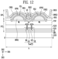
- FIG. 12 is a view of a first bank pattern illustrated in FIG. 11 implemented according to another example embodiment and is a cross sectional view corresponding to the line II-II′ of FIG. 7 .
- FIG. 13 is a view of a second contact electrode illustrated in FIG. 11 implemented according to another example embodiment and is a cross-sectional view corresponding to the line II-II′ of FIG. 7 .
- FIG. 14 A is a schematic enlarged plan view of a portion EA 1 of FIG. 8 .
- FIG. 14 B is a schematic enlarged plan view of a portion EA 2 of FIG. 8 .
- FIGS. 15 A- 15 G are schematic plan views of first and second electrodes illustrated in FIG. 7 implemented according to some other example embodiments.
- FIG. 16 is a schematic plan view illustrating a pixel according to another example embodiment of the present disclosure.
- FIG. 17 is a cross-sectional view taken along the line IV-IV′ of FIG. 16 .
- FIG. 18 is a cross-sectional view taken along the line V-V′ of FIG. 16 .
- FIG. 19 A is a schematic enlarged plan view of a portion EA 3 of FIG. 16 .
- FIG. 19 B is a schematic enlarged plan view of a portion EA 4 of FIG. 16 .
- FIGS. 20 A- 20 G are schematic plan views of first and second contact electrodes of FIG. 16 implemented according to some other example embodiments.
- FIG. 21 is a schematic view illustrating a pixel according to still another example embodiment of the present disclosure and is a schematic plan view of a pixel including only some components of a display element layer.
- first”, “second”, “third”, etc. may be used herein to describe various elements, components, regions, layers and/or sections, these elements, components, regions, layers and/or sections should not be limited by these terms. These terms are only used to distinguish one element, component, region, layer or section from another element, component, region, layer or section. Thus, a first element, component, region, layer or section discussed herein could be termed a second element, component, region, layer or section, without departing from the scope of the present disclosure.
- spatially relative terms such as “beneath”, “below”, “lower”, “under”, “above”, “upper” and the like, may be used herein for ease of description to describe one element or feature's relationship to another element(s) or feature(s) as illustrated in the figures. It will be understood that such spatially relative terms are intended to encompass different orientations of the device in use or in operation, in addition to the orientation depicted in the figures. For example, if the device in the figures is turned over, elements described as “below” or “beneath” or “under” other elements or features would then be oriented “above” the other elements or features. Thus, the example terms “below” and “under” can encompass both an orientation of above and below.
- the device may be otherwise oriented (e.g., rotated 90 degrees or at other orientations) and the spatially relative descriptors used herein should be interpreted accordingly.
- a layer is referred to as being “between” two layers, it can be the only layer between the two layers, or one or more intervening layers may also be present.
- the term “and/or” includes any and all combinations of one or more of the associated listed items. Expressions such as “at least one of,” when preceding a list of elements, modify the entire list of elements and do not modify the individual elements of the list. Further, the use of “may” when describing embodiments of the present disclosure refers to “one or more embodiments of the present disclosure”. Also, the term “exemplary” is intended to refer to an example or illustration. As used herein, the terms “use,” “using,” and “used” may be considered synonymous with the terms “utilize,” “utilizing,” and “utilized,” respectively.
- FIG. 1 is a schematic perspective view illustrating a light-emitting element according to one or more example embodiments of the present disclosure
- FIG. 2 is a cross-sectional view of the light-emitting element of FIG. 1
- FIG. 3 is a schematic perspective view illustrating a light-emitting element according to another example embodiment of the present disclosure
- FIG. 4 is a cross-sectional view of the light-emitting element of FIG. 3 .
- the type and/or shape of a light-emitting element is not limited to the example embodiments illustrated in FIGS. 1 - 4 .
- a light-emitting element LD may include a first semiconductor layer 11 , a second semiconductor layer 13 , and an active layer 12 interposed between the first semiconductor layer 11 and the second semiconductor layer 13 .
- the light-emitting element LD may implement a light-emitting stack in which the first semiconductor layer 11 , the active layer 12 , and the second semiconductor layer 13 are sequentially stacked.
- the light-emitting element LD may be provided in a shape that extends in one direction.
- an extending direction of the light-emitting element LD is a length direction thereof, the light-emitting element LD may have one end portion (or lower end portion) and the other end portion (or upper end portion) in the extending direction.
- One semiconductor layer of the first and second semiconductor layers 11 and 13 may be disposed at one end portion (lower end portion) of the light-emitting element LD, and the other semiconductor layer of the first and second semiconductor layers 11 and 13 may be disposed at the other end portion of the light-emitting element LD.
- the first semiconductor layer 11 may be disposed at one end portion (or lower end portion) of the light-emitting element LD, and the second semiconductor layer 13 may be disposed at the other end portion (or upper end portion) of the light-emitting element LD.
- the light-emitting element LD may be provided in various shapes.
- the light-emitting element LD may have a rod-like shape or a bar-like shape which is long in a length direction thereof (i.e., has an aspect ratio greater than one).
- a length L of the light-emitting element LD in the length direction thereof may be greater than a diameter D (or width of a cross section) thereof.
- the light-emitting element LD may include, for example, a light-emitting diode (LED) manufactured in a very small size such that the diameter D and/or the length L may be in a micro-scale or a nano-scale.
- LED light-emitting diode
- the diameter D of the light-emitting element LD may be in a range of about 0.5 ⁇ m to about 500 ⁇ m, and the length L thereof may be in a range of about 1 ⁇ m to about 10 ⁇ m.
- the diameter D and the length L of the light-emitting element LD are not limited thereto, and the size of the light-emitting element LD may be changed such that the light-emitting element LD meets requirements (or design conditions) of a lighting device or a self-luminous display device to which the light-emitting element LD is applied.
- the first semiconductor layer 11 may include at least one n-type semiconductor layer.
- the first semiconductor layer 11 may be an n-type semiconductor layer which includes any one semiconductor material selected from InAlGaN, GaN, AlGaN, InGaN, AlN, and InN and is doped with a first conductive type dopant (or n-type dopant) such as silicon (Si), germanium (Ge), tin (Sn), or the like.
- a material constituting the first semiconductor layer 11 is not limited thereto, and the first semiconductor layer 11 may be made of various materials.
- the first semiconductor layer 11 may include a gallium nitride (GaN) semiconductor material doped with the first conductive dopant (or n-type dopant).
- the first semiconductor layer 11 may be an n-type GaN semiconductor layer.
- the first semiconductor layer 11 may include an upper surface in contact with the active layer 12 in a direction of the length L of the light-emitting element LD and a lower surface exposed to the outside.
- the lower surface of the first semiconductor layer 11 may be one end portion (or lower end portion) of the light-emitting element LD.
- the active layer 12 may be disposed on the first semiconductor layer 11 and may be formed to have a single or multi-quantum well structure.
- a barrier layer (not illustrated), a strain reinforcing layer, and a well layer may be repeatedly and periodically stacked as one unit.
- the strain strengthening layer may have a smaller lattice constant than the barrier layer to further strengthen strain, for example, compression stress applied to the well layer.
- the structure of the active layer 12 is not limited to the above-described example embodiment.
- the active layer 12 may emit light having a wavelength of 400 nm to 900 nm and may have a double hetero structure.
- a clad layer (not illustrated) doped with a conductive dopant may be formed on an upper portion and/or a lower portion of the active layer 12 in the direction of the length of the light-emitting element LD.
- the clad layer may be formed as an AlGaN layer or an InAlGaN layer.
- a material such as AlGaN or InAlGaN may be used to form the active layer 12 , and in some cases, various materials may constitute the active layer 12 .
- the active layer 12 may have a first surface in contact with the first semiconductor layer 11 and a second surface in contact with the second semiconductor layer 13 .
- the first surface and the second surface of the active layer 12 may face each other in the direction of the length L of the light-emitting element LD.
- the light-emitting element LD When a voltage greater than equal to a certain voltage is applied to both ends of the light-emitting element LD, electrons-hole pairs combine, and thus, the light-emitting elements LD emits light.
- the light-emitting element LD may be used as a light source (or light-emitting source) of various light-emitting elements including pixels of a display device.
- the second semiconductor layer 13 may be disposed on the second surface of the active layer 12 and may include a semiconductor layer which is a different type from the first semiconductor layer 11 .
- the second semiconductor layer 13 may include at least one p-type semiconductor layer.
- the second semiconductor layer 13 may include a p-type semiconductor layer which includes at least one semiconductor material selected from InAlGaN, GaN, AlGaN, InGaN, AlN, and InN and is doped with a second conductive type dopant (or p-type dopant) such as magnesium (Mg).
- Mg magnesium
- the material constituting the second semiconductor layer 13 is not limited thereto, and the second semiconductor layer 13 may be made of various materials.
- the second semiconductor layer 13 may include a gallium nitride (GaN) semiconductor material doped with the second conductive dopant (or p-type dopant).
- the second semiconductor layer 13 may be a p-type GaN semiconductor.
- the second semiconductor layer 13 may have a lower surface in contact with the active layer 12 in the direction of the length L of the light-emitting element LD and an upper surface exposed to the outside.
- the upper surface of the second semiconductor layer 13 may be the other end portion (or upper end portion) of the light-emitting element LD.
- the first semiconductor layer 11 and the second semiconductor layer 13 may have different thicknesses in the direction of the length of the light-emitting element LD.
- the first semiconductor layer 11 may have a thickness that is relatively greater than that of the second semiconductor layer 13 in the direction of the length L of the light-emitting element LD.
- the active layer 12 of the light-emitting element LD may be positioned closer to the upper surface of the second semiconductor layer 13 than the lower surface of the first semiconductor layer 11 .
- each of the first semiconductor layer 11 and the second semiconductor layer 13 are illustrated as being formed as one layer, but the present disclosure is not limited thereto.
- each of the first semiconductor layer 11 and the second semiconductor layer 13 may further include at least one layer, for example, a clad layer and/or a tensile strain barrier reducing layer (TSBR) according to a material of the active layer 12 .
- the TSBR layer may be a strain reducing layer disposed between semiconductor layers having different lattice structures to serve as a buffer for reducing a lattice constant difference.
- the TSBR layer may be made of a p-type semiconductor layer such as p-GaInP, p-AlInP, or p-AlGaInP, but the present disclosure is not limited thereto.
- the light-emitting element LD may further include an additional electrode (not illustrated, hereinafter, referred to as “first additional electrode”) disposed on the second semiconductor layer 13 .
- the light-emitting element LD may further include another additional electrode (not illustrated, hereinafter referred to as “second additional electrode”) disposed at one end of the first semiconductor layer 11 .
- first and second additional electrodes may be an ohmic contact electrode, but the present disclosure is not limited thereto.
- the first and second additional electrodes may be schottky contact electrodes.
- the first and second additional electrodes may include a conductive material (or substance).
- the first and second additional electrodes may include an opaque metal using chromium (Cr), titanium (Ti), aluminum (Al), gold (Au), nickel (Ni), and an oxide or alloy thereof, alone or in a mixture.
- the first and second additional electrodes may include a transparent conductive oxide such as indium tin oxide (ITO), indium zinc oxide (IZO), zinc oxide (ZnO), indium gallium zinc oxide (IGZO), or indium tin zinc oxide (ITZO).
- ITO indium tin oxide
- IZO indium zinc oxide
- ZnO zinc oxide
- IGZO indium gallium zinc oxide
- ITZO indium tin zinc oxide
- first and second additional electrodes may be the same or different.
- the first and second additional electrodes may be substantially transparent or semitransparent. Accordingly, light generated by the light-emitting element LD may be emitted to the outside of the light-emitting element LD by passing through the first and second additional electrodes. According to one or more example embodiments, when light generated by the light-emitting element LD does not pass through the first and second additional electrodes and is emitted to the outside of the light-emitting element LD through a region excluding both ends of the light-emitting-element LD, the first and second additional electrodes may include an opaque metal.
- the light-emitting element LD may further include an insulating film 14 .
- the insulating film 14 may be omitted and may be provided to cover only a portion of the first semiconductor layer 11 , the active layer 12 , and the second semiconductor layer 13 .
- the insulating film 14 may prevent an electrical short circuit that may occur when the active layer 12 comes into contact with conductive materials other than the first and second semiconductor layers 11 and 13 .
- the insulating film 14 may reduce or minimize the surface defects of the light-emitting element LD and may improve a lifetime and efficiency of the light-emitting element LD.
- the insulating film 14 may prevent an undesired short circuit that may occur between the light-emitting elements LD. As long as the active layer 12 can be prevented from being short-circuited with an external conductive material, there is no limit or restriction as to whether the insulating film 14 should be provided.
- the insulating film 14 may be provided in a form which entirely surrounds (or partially surrounds) an outer surface (e.g., an outer peripheral or circumferential surface) of the light-emitting stack including the first semiconductor layer 11 , the active layer 12 , and the second semiconductor layer 13 .
- FIG. 1 illustrates a state in which a portion of the insulating film 14 is deleted, and the first semiconductor layer 11 , the active layer 12 , and the second semiconductor layer 13 included in the light-emitting element LD may be actually surrounded by the insulating film 14 .
- the insulating film 14 is provided in a form which entirely surrounds an outer surface (e.g., an outer peripheral or circumferential surface) of each of the first semiconductor layer 11 , the active layer 12 , and the second semiconductor layer 13 , but the present disclosure is limited thereto.
- the insulating film 14 may entirely surround an outer surface (e.g., an outer peripheral or circumferential surface) of each of the first semiconductor layer 11 , the active layer 12 , the second semiconductor layer 13 , and the first additional electrode.
- the insulating film 14 may not entirely surround the outer surface (e.g., an outer peripheral or circumferential surface) of the first additional electrode or may surround only a portion of the outer surface (e.g., an outer peripheral or circumferential surface) of the first additional electrode and not surround the rest of the outer surface (e.g., an outer peripheral or circumferential surface) of the first additional electrode. Furthermore, according to some example embodiments, when the first additional electrode is disposed at the other end portion (or upper end portion) of the light-emitting element LD and the second additional electrode is disposed at one end portion (or lower end portion) of the light-emitting element LD, the insulating film 14 may expose at least one region of each of the first and second additional electrodes. In another example embodiment, the insulating film 14 may not be provided.
- the insulating film 14 may include a transparent insulating material.
- the insulating film 14 may include at least one insulating material selected from the group consisting of silicon oxide (SiO x ), silicon nitride (SiN x ), silicon oxynitride (SiO x N y ), aluminum oxide (AlO x ), and titanium dioxide (TiO 2 ).
- SiO x silicon oxide
- SiN x silicon nitride
- SiO x N y silicon oxynitride
- AlO x aluminum oxide
- TiO 2 titanium dioxide
- the present disclosure is not limited thereto, and various materials having insulating properties may be used as the material of the insulating film 14 .
- the active layer 12 can be prevented from being short-circuited with electrodes which are not illustrated.
- the insulating film 14 may reduce or minimize the surface defects of the light-emitting element LD and may improve a lifetime and luminance efficiency of the light-emitting element LD.
- the insulating film 14 may prevent an undesired short circuit that may occur between the light-emitting elements LD.
- a light-emitting element LD′ may include a light-emitting pattern 10 ′ having a core-shell structure.
- a first semiconductor layer 11 ′ may be positioned at a core (that is, a center) of the light-emitting element LD′, and an active layer 12 ′ may be provided or formed in a form which surrounds an outer surface (e.g., an outer peripheral or circumferential surface) of the first semiconductor layer 11 ′ in a direction of a length L of the light-emitting element LD′.
- a second semiconductor layer 13 ′ may be provided or formed in a form which surrounds the active layer 12 ′ in the direction of the length L of the light-emitting element LD′.
- the light-emitting element LD′ may further include an additional electrode (e.g., 15 ′) surrounding at least one side of the second semiconductor layer 13 ′.
- the light-emitting element LD′ may further include an insulating film 14 ′ which is provided on an outer surface (e.g., an outer peripheral or circumferential surface) of the light-emitting pattern 10 ′ having a core-shell structure and includes a transparent insulating material.
- the light-emitting element LD may be used as a light-emitting source for various display devices.
- the light-emitting element LD (or LD′) may be manufactured through a surface treatment process. For example, when a plurality of light-emitting elements LD (or LD′) are mixed in a flowable solution (or solvent) and provided to each pixel area (for example, an emission area of each pixel), the light-emitting elements LD (or LD′) may be surface-treated so as to be uniformly sprayed without being non-uniformly aggregated in the solution.
- a light-emitting unit (or light-emitting device) including the above-described light-emitting element LD (or LD′) may be used in various types of electronic devices, such as display devices, which require a light source.
- the light-emitting elements LD (or LD′) when the plurality of light-emitting elements LD (or LD′) are disposed in a pixel area of each pixel of a display panel, the light-emitting elements LD (or LD′) may be used as light sources for each pixel.
- the application field of the light-emitting element LD (or LD′) is not limited to the above-described example.
- the light-emitting element LD (or LD′) may be used in other types of electronic devices, such as lighting devices, which require a light source.
- FIG. 5 is a view illustrating a display device according to one or more example embodiments, and particularly, a schematic plan view of a display device using any one light-emitting element of the light-emitting elements illustrated in FIGS. 1 - 4 as a light source.
- the structure of the display device is briefly illustrated based on a display area DA in which an image is displayed.
- at least one driver for example, a scan driver or a data driver
- a plurality of signal lines may be further disposed in the display device.
- the display device may include a substrate SUB, a plurality of pixels PXL which are provided on the substrate SUB, each of the pixels PXL including at least one light-emitting element LD, a driver which is provided on the substrate SUB to drive the pixels PXL, and a line portion which connects the pixels PXL and the driver.
- the display device is an electronic device, in which a display surface is applied to at least one surface thereof, such as a smartphone, a television, a tablet personal computer (PC), a mobile phone, an image phone, an e-book reader, a desktop PC, a laptop PC, a netbook computer, a workstation, a server, a personal digital assistant (PDA), a portable multimedia player (PMP), an MP3 player, a medical device, a camera, or a wearable device, the present disclosure may be applied.
- a display surface is applied to at least one surface thereof, such as a smartphone, a television, a tablet personal computer (PC), a mobile phone, an image phone, an e-book reader, a desktop PC, a laptop PC, a netbook computer, a workstation, a server, a personal digital assistant (PDA), a portable multimedia player (PMP), an MP3 player, a medical device, a camera, or a wearable device
- PDA personal digital assistant
- PMP portable multimedia player
- the display device may be classified into a passive matrix type display device and an active matrix type display device according to a method of driving the light-emitting element LD.
- each of the pixels PXL may include a driving transistor which controls an amount of a current supplied to the light-emitting element LD, a switching transistor which transmits a data signal to the driving transistor, and the like.
- a passive matrix type display device in which turning-on is performed for each group of the pixel PXL, may also use components (for example, first and second electrodes) for driving the light-emitting element LD.
- the substrate SUB may include the display area DA and a non-display area NDA.
- the display area DA may be disposed in a central area of the display device, and the non-display area NDA may be disposed in an edge area of the display device to surround the display area DA along the periphery of the display area DA.
- the positions of the display area DA and the non-display area NDA are not limited thereto, and the positions thereof may be changed.
- the display area DA may be an area in which the pixels PXL displaying an image are provided.
- the non-display area NDA may be an area in which the driver for driving the pixels PXL and a portion of the line portion for connecting the pixels PXL and the driver are provided.
- the plurality of pixels PXL may be substantially disposed in the display area DA of the substrate SUB.
- the display area DA may have various shapes.
- the display area DA may be provided in a closed polygon having sides formed of straight lines.
- the display area DA may be provided in a circle shape and/or an ellipse shape having sides formed of curved lines.
- the display area DA may be provided in various shapes, such as a semicircle and a semi-ellipse, which include sides formed of straight lines and curved lines.
- the non-display area NDA may be provided on at least one side of the display area DA. In one or more example embodiments of the present disclosure, the non-display area NDA may surround a periphery (or edge) of the display area DA.
- the line portion connected to the pixels PXL and the driver for driving the pixels PXL may be provided in the non-display area NDA.
- the line portion may electrically connect the driver and the pixels PXL.
- the line portion may provide a signal to each pixel PXL and may be a fan-out line portion connected to signal lines, for example, a scan line, a data line, and an emission control line.
- the line portion may be a fan-out line portion connected to signal lines connected to each pixel PXL, for example, a control line and a sensing line in order to compensate for changes in electrical characteristics of each pixel PXL in real time.
- the substrate SUB may include a transparent insulating material to transmit light.
- the substrate SUB may be a rigid substrate or a flexible substrate.
- the substrate SUB may be provided as the display area DA, and thus, the pixels PXL may be disposed therein.
- the remaining area of the substrate SUB may be provided as the non-display area NDA.
- the substrate SUB may include the display area DA including pixel areas in which the pixels PXL are formed and include the non-display area NDA disposed around (or adjacent to) the display area DA.
- the pixels PXL may each be provided in the display area DA of the substrate SUB.
- the pixels PXL may be arranged in the display area DA in a stripe arrangement structure or a pentile arrangement structure, but the present disclosure is not limited thereto.
- Each pixel PXL may include at least one light-emitting element LD driven by a corresponding scan signal and data signal.
- the light-emitting element LD may have a small size ranging from a nanoscale to a microscale and may be parallel with light-emitting elements disposed adjacent thereto, but the present disclosure is not limited thereto.
- the light-emitting element LD may constitute a light source of each pixel PXL.
- Each pixel PXL may include at least one light source driven by certain signals (for example, a scan signal and a data signal) and/or certain powers (for example, first driving power and second driving power).
- each pixel PXL may include the light-emitting elements LD illustrated in FIGS. 1 - 4 , for example, at least one micro light-emitting element LD having a size ranging from a nanoscale to a microscale.
- a type of the light-emitting element LD usable as the light source of each pixel PXL is not limited thereto.
- the color, type, and/or number of the pixels PXL are not particularly limited, and as an example, the color of light emitted from each pixel PXL may be variously changed.
- the driver may provide a certain signal and certain power to each pixel PXL through the line portion, thereby controlling the driving of the pixel PXL.
- the driver may include a scan driver which provides scan signals to the pixels PXL through scan lines, an emission driver which provides emission control signals to the pixels PXL through emission control lines, a data driver which provides data signals to the pixels PXL through data lines, and a timing controller.
- the timing controller may control the scan driver, the emission driver, and the data driver.
- FIGS. 6 A- 6 C are circuit diagrams illustrating electrical connection relationships of components included in one pixel illustrated in FIG. 5 according to various example embodiments.
- FIGS. 6 A- 6 C illustrate electrical connection relationships of components included in pixels PXL applicable to an active type display device according to different example embodiments.
- the types of the components included in the pixel PXL to which the example embodiment of the present disclosure is applicable are not limited thereto.
- each of the pixels PXL illustrated in FIGS. 6 A- 6 C may be any one of the pixels PXL provided in the display device of FIG. 5 , and the pixels PXL may have substantially the same or similar structure.
- one pixel PXL may include a light-emitting unit EMU which generates light having luminance corresponding to a data signal.
- the pixel PXL may further optionally include a pixel circuit 144 for driving the light-emitting unit EMU.
- the light-emitting unit EMU may include a plurality of light-emitting elements LD connected in parallel with each other between a first power line PL 1 to which a voltage of a first driving power source VDD is applied and a second power line PL 2 to which a voltage of a second driving power source VSS is applied.
- the light-emitting unit EMU may include a first electrode EL 1 (or “first alignment electrode”) connected to the first driving power source VDD through the pixel circuit 144 and the first power line PL 1 , a second electrode EL 2 (or “second alignment electrode”) connected to the second driving power source VSS through the second power line PL 2 , and the plurality of light-emitting elements LD connected in parallel with each other in the same direction between the first electrode EL 1 and the and second electrode EL 2 .
- the first electrode EL 1 may be an anode
- the second electrode EL 2 may be a cathode.
- each of the light-emitting elements LD included in the light-emitting unit EMU may include one end connected to the first driving power source VDD through the first electrode EL 1 and the other end connected to the second driving power source VSS through the second electrode EL 2 .
- the first driving power source VDD and the second driving power source VSS may have different potentials.
- the first driving power source VDD may be set as a high potential power source
- the second driving power source VSS may be set as a low potential power source.
- a potential difference between the first driving power source VDD and the second driving power source VSS may be set to be greater than or equal to a threshold voltage of the light-emitting elements LD during an emission period of the pixel PXL.
- each of the light-emitting elements LD connected in parallel with each other in the same direction (for example, a forward direction) between the first electrode EL 1 and the second electrode EL 2 , to which voltages having different potentials are supplied, may each constitute an effective light source.
- the effective light sources may be clustered to constitute the light-emitting unit EMU of the pixel PXL.
- the light-emitting elements LD of the light-emitting unit EMU may emit light at luminance corresponding to a driving current supplied through the corresponding pixel circuit 144 .
- the pixel circuit 144 may supply a driving current corresponding to a gray level value of corresponding frame data to the light-emitting unit EMU.
- the driving current supplied to the light-emitting unit EMU may be divided to flow in the light-emitting elements LD. Accordingly, while each light-emitting element LD may emit light at luminance corresponding to a current flowing therein, the light-emitting unit EMU may emit light at luminance corresponding to the driving current.
- FIGS. 6 A- 6 C illustrate example embodiments in which the light-emitting elements LD are connected in the same direction (e.g., forward direction) between the first driving power source VDD and the second driving power source VSS, but the present disclosure is not limited thereto.
- the light-emitting unit EMU may further include at least one ineffective light source, for example, a reverse light-emitting element LDr, in addition to the light-emitting-elements LD constituting the effective light sources.
- the reverse light-emitting element LDr is connected in parallel with the light-emitting elements LD between the first electrode EL 1 and the second electrode EL 2 and may be connected between the first electrode EL 1 and the second electrode EL 2 in an opposite direction as the light-emitting elements LD.
- the reverse light-emitting element LDr maintains an inactive state (or a reverse biased state) even when a certain driving voltage (for example, a driving voltage in a forward direction) is applied between the first electrode EL 1 and the second electrode EL 2 , and thus, a current does not substantially flow in the reverse light-emitting element LDr.
- the pixel circuit 144 may be connected to a scan line Si and a data line Dj of a corresponding pixel PXL.
- the pixel circuit 144 of the pixel PXL may be connected to an i th scan line Si and a j th data line Dj in the display area DA.
- the pixel circuit 144 may include first and second transistors T 1 and T 2 and a storage capacitor Cst.
- the structure of the pixel circuit 144 is not limited to the example embodiments illustrated in FIGS. 6 A- 6 C .
- the pixel circuit 144 may include the first and second transistors T 1 and T 2 and the storage capacitor Cst.
- a first terminal of the second transistor T 2 (e.g., a switching transistor) may be connected to the j th data line Dj, and a second terminal thereof may be connected to a first node N 1 .
- the first terminal and the second terminal of the second transistor T 2 may be different terminals, and for example, when the first terminal is a source electrode, the second terminal may be a drain electrode.
- a gate electrode of the second transistor T 2 may be connected to the i th scan line Si.
- the second transistor T 2 may be turned on when a scan signal having a voltage (for example, a low voltage), at which the second transistor T 2 may be turned on, is supplied from the i th scan line Si, thereby electrically connecting the j th data line Dj and the first node N 1 .
- a data signal of a corresponding frame is supplied to the j th data line Dj, and thus, the data signal is transmitted to the first node N 1 .
- the data signal transmitted to the first node N 1 is charged in the storage capacitor Cst, for example, the storage capacitor Cst may be charged according to the data signal from the j th data line Dj transmitted to the first node N 1 .
- a first terminal of the first transistor T 1 (e.g., a driving transistor) may be connected to the first driving power source VDD, and a second terminal thereof may be electrically connected to the first electrode EL 1 of each of the light-emitting elements LD.
- a gate electrode of the first transistor T 1 may be connected to the first node N 1 .
- the first transistor T 1 controls an amount of a driving current supplied to the light-emitting elements LD in response to a voltage of the first node N 1 .
- One electrode of the storage capacitor Cst may be connected to the first driving power source VDD, and the other electrode thereof may be connected to the first node N 1 .
- the storage capacitor Cst may be charged with a voltage corresponding to a data signal supplied to the first node N 1 and may maintain the charged voltage until a data signal of a next frame is supplied.
- FIG. 6 A illustrates the pixel circuit 144 including the second transistor T 2 for transmitting a data signal into the pixel PXL, the storage capacitor Cst for storing the data signal, and the first transistor T 1 for supplying a driving current corresponding to the data signal to the light-emitting elements LD.
- the present disclosure is not limited thereto, and the structure of the pixel circuit 144 may be variously changed and implemented.
- the pixel circuit 144 may further additionally include other circuit elements such as at least one transistor element, which may include a transistor element for compensating for a threshold voltage of the first transistor T 1 , a transistor element for initializing the first node N 1 , and/or a transistor element for controlling emission times of the light-emitting elements LD, and a boosting capacitor for boosting a voltage of the first node N 1 .
- the transistors included in the pixel circuit 144 for example, the first and second transistors T 1 and T 2 are all illustrated as being p-type transistors, but the present disclosure is not limited thereto.
- at least one of the first and second transistors T 1 and T 2 included in the pixel circuit 144 may be changed to an n-type transistor.
- the pixel circuit 144 may be further connected to at least one other scan line according to some example embodiments.
- the pixel circuit 144 of the pixel PXL may be further connected to an i ⁇ 1 th scan line Si ⁇ 1 (e.g., a previous scan line) and/or an i+1 th scan line Si+1 (e.g., a next scan line).
- the pixel circuit 144 may be further connected to a third power source in addition to the first and second driving power sources VDD and VSS.
- the pixel circuit 144 may also be connected to an initialization power source Vint.
- the pixel circuit 144 may include first to seventh transistors T 1 to T 7 and the storage capacitor Cst.
- a first terminal of the first transistor T 1 (e.g., the driving transistor), for example, a source electrode thereof may be connected to the first driving power source VDD through the fifth transistor T 5 , and a second terminal thereof, for example, a drain electrode thereof may be electrically connected to one end of the light-emitting elements LD through the sixth transistor T 6 .
- a gate electrode of the first transistor T 1 may be connected to the first node N 1 .
- the first transistor T 1 controls a driving current flowing between the first driving power source VDD and the second driving power source VSS through the light-emitting elements LD in response to a voltage of the first node N 1 .
- the second transistor T 2 (e.g., the switching transistor) may be connected between the j th data line Dj connected to the pixel PXL and the first terminal of the first transistor T 1 .
- a gate electrode of the second transistor T 2 may be connected to the i th scan line Si connected to the pixel PXL.
- the second transistor T 2 may be turned on when a scan signal having a gate-on voltage (for example, a low voltage) is supplied from the i th scan line Si, thereby electrically connecting the j th data line Dj and the first terminal of the first transistor T 1 . Therefore, when the second transistor T 2 is turned on, a data signal supplied from the j th data line Dj may be transmitted to the first transistor T 1 .
- a gate-on voltage for example, a low voltage
- the third transistor T 3 may be connected between the second terminal of the first transistor T 1 and the first node N 1 .
- a gate electrode of the third transistor T 3 may be connected to the i th scan line Si.
- the third transistor T 3 may be turned on when a scan signal having a gate-on voltage (for example, a low voltage) is supplied from the i th scan line Si, thereby electrically connecting the second terminal of the first transistor T 1 and the first node N 1 .
- the fourth transistor T 4 may be connected between the first node N 1 and an initialization power line IPL to which the initialization power source Vint is connected.
- a gate electrode of the fourth transistor T 4 may be connected to a previous scan line, for example, an i ⁇ 1 th scan line Si ⁇ 1.
- the fourth transistor T 4 may be turned on when a scan signal having a gate-on voltage (for example, a low voltage) is supplied to the i ⁇ 1 th scan line Si ⁇ 1, thereby transmitting a voltage of the initialization power source Vint to the first node N 1 .
- the initialization power source Vint may have a voltage less than or equal to a minimum voltage of a data signal.
- the fifth transistor T 5 may be connected between the first power driving source VDD and the first terminal of the first transistor T 1 .
- a gate electrode of the fifth transistor T 5 may be connected to a corresponding emission control line, for example, an i th emission control line Ei.
- the fifth transistor T 5 may be turned off when an emission control signal having a gate-off voltage (for example, a high voltage) is supplied to the i th emission control line Ei, and may be turned on otherwise.
- the sixth transistor T 6 may be connected between the second terminal of the first transistor T 1 and one end of the light-emitting elements LD.
- a gate electrode of the sixth transistor T 6 may be connected to the i th emission control line Ei.
- the sixth transistor T 6 may be turned off when an emission control signal having a gate-off voltage (for example, a high voltage) is supplied to the i th emission control line Ei, and may be turned on otherwise.
- a gate-off voltage for example, a high voltage
- the seventh transistor T 7 may be connected between one end of the light-emitting elements LD and the initialization power line IPL.
- a gate electrode of the seventh transistor T 7 may be connected to any one of scan lines in a next row, for example, an i+1 th scan line Si+1.
- the seventh transistor T 7 may be turned on when a scan signal having a gate-on voltage (for example, a low voltage) is supplied to the i+1 th scan line Si+1, thereby supplying a voltage of the initialization power source Vint to one end of the light-emitting elements LD.
- a gate-on voltage for example, a low voltage
- the storage capacitor Cst may be connected between the first driving power source VDD and the first node N 1 .
- the storage capacitor Cst may store a data signal supplied to the first node N 1 during each frame period and a voltage corresponding to a threshold voltage of the first transistor T 1 .
- the transistors included in the pixel circuit 144 for example, the first to seventh transistors T 1 to T 7 are all illustrated as being p-type transistors, but the present disclosure is not limited thereto.
- at least one of the first to seventh transistors T 1 to T 7 may be changed to an n-type transistor.
- the configuration of the pixel circuit 144 is not limited to the example embodiments illustrated in FIGS. 6 A and 6 B .
- the pixel circuit 144 may be configured as in the example embodiment shown in FIG. 6 C .
- the pixel circuit 144 may be further connected to a control line CLi and a sensing line SENj.
- the pixel circuit 144 may be connected to an i th control line CLi and a j th sensing line SENj in the display area DA.
- the pixel circuit 144 may further include a third transistor T 3 in addition to the first and second transistors T 1 and T 2 illustrated in FIG. 6 A .
- the third transistor T 3 is connected between the first transistor T 1 and the j th sensing line SENj.
- one electrode of the third transistor T 3 may be connected to a first terminal (for example, a source electrode) of the first transistor T 1 connected to the first electrode EL 1
- the other electrode of the third transistor T 3 may be connected to the j th sensing line SENj.
- a gate electrode of the third transistor T 3 is connected to the i th control line CLi.
- the gate electrode of the third transistor T 3 may be connected to the i th scan line Si.
- the third transistor T 3 is turned on by a control signal having a gate-on voltage (for example, a high level voltage) supplied to the i th control line CLi during a certain sensing period, thereby electrically connecting the j th sensing line SENj and the first transistor T 1 .
- the sensing period may be a period for extracting characteristic information (for example, a threshold voltage or the like of the first transistor T 1 ) of each of the pixels PXL disposed in the display area DA.
- characteristic information for example, a threshold voltage or the like of the first transistor T 1
- a certain reference voltage, at which the first transistor T 1 may be turned on may be supplied to the first node N 1 through the j th data line Dj and the second transistor T 2 , or each pixel PXL may be connected to a current source or the like to turn the first transistor T 1 on.
- a control signal having a gate-on voltage may be supplied to the third transistor T 3 (e.g., via the control line CLi) to turn the third transistor T 3 on, thereby connecting the first transistor T 1 to the j th sensing line SENj.
- characteristic information of each pixel PXL including the threshold voltage or the like of the first transistor T 1 may be extracted through the j th sensing line SENj described above. The extracted characteristic information may be used to convert image data so that a characteristic deviation between pixels PXL is compensated for.
- the storage capacitor Cst may be connected between the first node N 1 and the source electrode of the first transistor T 1 .
- the storage capacitor Cst may store a voltage corresponding to a data signal supplied to the first node N 1 during each frame period and a voltage corresponding to a threshold voltage of the first transistor T 1 .
- the first to third transistors T 1 to T 3 are all illustrated as being n-type transistors, but the present disclosure is not limited thereto. For example, at least one of the first to third transistors T 1 to T 3 may be changed to a p-type transistor.
- FIG. 6 C illustrates an example embodiment in which the light-emitting unit EMU is connected between the pixel circuit 144 and the second driving power source VSS, but the light-emitting unit EMU may be connected between the first driving power source VDD and the pixel circuit 144 .
- FIGS. 6 A- 6 C illustrate the example embodiments in which the light-emitting elements LD constituting the light-emitting unit EMU are all connected in parallel, but the present disclosure is not limited thereto.
- the light-emitting unit EMU may include at least one series stage including the plurality of light-emitting elements LD connected in parallel with each other.
- the light-emitting unit EMU may also have a series-and-parallel mixed structure.
- each pixel PXL may be provided inside a passive light-emitting display device.
- the pixel circuit 144 may be omitted, and both ends of the light-emitting elements LD included in the light-emitting unit EMU may be directly connected to the i th scan line Si, the j th data line Dj, the first power line PL 1 to which the first driving power source VDD is connected, the second power line PL 2 to which the second driving power source VSS is connected, and/or a certain control line (e.g., CLi).
- a certain control line e.g., CLi
- FIG. 7 is a schematic plan view illustrating one of the pixels illustrated in FIG. 5 .
- FIG. 8 is a plan view illustrating only first and second connection lines, first and second electrodes, and a first insulating layer of FIG. 7 .
- FIG. 9 is a cross-sectional view taken along the line I-I′ of FIG. 7 .
- FIG. 10 is a cross-sectional view taken along the line II-II′ of FIG. 7 .
- FIG. 11 is a cross-sectional view taken along the line III-III′ of FIG. 7 .
- FIG. 12 is a view of a first bank pattern illustrated in FIG. 11 implemented according to another example embodiment and is a cross sectional view corresponding to the line II-II′ of FIG. 7 .
- FIG. 13 is a view of a second contact electrode illustrated in FIG. 11 implemented according to another example embodiment and is a cross-sectional view corresponding to the line II-II′ of FIG. 7 .
- FIG. 14 A is a schematic enlarged plan view of a portion EA 1 of FIG. 8 .
- FIG. 14 B is a schematic enlarged plan view of a portion EA 2 of FIG. 8 .
- the pixel illustrated in FIG. 7 may be the pixel illustrated in FIG. 6 A .
- transistors connected to light-emitting elements and signal lines connected to the transistors are omitted for convenience.
- one pixel PXL is simplified and illustrated by illustrating each electrode as a single-film electrode and illustrating each insulating layer as an insulating layer that is a single-film, but the present disclosure is not limited thereto.
- phrase “formed and/or provided on the same layer” may mean the phrase “formed through the same process,” and the phrase “formed and/or provided on different layers” may mean the phrase “formed through different processes.”
- connection between two components may mean that both electrical and physical connections are used.
- a lateral direction (or horizontal direction) in a plan view is expressed as a first direction DR 1
- a longitudinal direction (or vertical direction) in a plan view is expressed as a second direction DR 2
- a thickness direction of a substrate SUB on a cross section is expressed as a third direction DR 3 .
- the first to third directions DR 1 , DR 2 , and DR 3 may refer to directions indicated by the first to third directions DR 1 , DR 2 , and DR 3 , respectively.
- a display device may include a plurality of pixels PXL provided on the substrate SUB.
- the substrate SUB may include a transparent insulating material to transmit light.
- the substrate SUB may be a rigid substrate or a flexible substrate.
- the rigid substrate may be, for example, one of a glass substrate, a quartz substrate, a glass ceramic substrate, and a crystalline glass substrate.
- the flexible substrate may be one of a film substrate and a plastic substrate which include a polymer organic material.
- the flexible substrate may include at least one selected from polystyrene, polyvinyl alcohol, polymethyl methacrylate, polyethersulfone, polyacrylate, polyetherimide, polyethylene naphthalate, polyethylene terephthalate, polyphenylene sulfide, polyarylate, polyimide, polycarbonate, triacetate cellulose, and cellulose acetate propionate.
- a material constituting the substrate SUB may be variously changed and may also include fiber reinforced plastic (FRP) or the like.
- a material applied to the substrate SUB may have resistance (or heat resistance) to a high processing temperature in a manufacturing process of the display device.
- the substrate SUB may include a display area DA including at least one pixel area PXA in which the pixels PXL are disposed, and a non-display area NDA disposed around (or adjacent to) the display area DA.
- the pixels PXL may be arranged in a matrix form or a stripe form according to a plurality of pixel rows extending in the first direction DR 1 in the display area DA on the substrate SUB and a plurality of pixel columns extending in the second direction DR 2 that is different from the first direction DR 1 , for example, a direction crossing the first direction DR 1 , but the present disclosure is not limited thereto.
- the pixels PXL may be provided in the display area DA on the substrate SUB in various arrangement forms.
- the pixel area PXA in which each pixel PXL is provided (or formed), includes an emission area in which light is emitted and a peripheral area which is adjacent to the emission area (or surrounds the periphery of the emission area, in other words, the peripheral area may be adjacent to the emission area and/or may surround the emission area along the periphery of the emission area).
- the peripheral area may include a non-emission area in which light is not emitted.
- a line portion electrically connected to the pixels PXL may be positioned on the substrate SUB.
- the line portion may include a plurality of signal lines transmitting certain signals (or certain voltages) to each pixel PXL.
- the signal lines may include an i th scan line Si for transmitting a scan signal to each pixel PXL, a j th data line Dj for transmitting a data signal to each pixel PXL, and power lines PL 1 and PL 2 for transmitting driving power to each pixel PXL.
- the line portion may further include an emission control line (e.g., Ei) that transmits an emission control signal to each pixel PXL.
- the line portion may further include a sensing line (SENj) and a control line (CLi) connected to each pixel PXL.
- Each pixel PXL may be provided on the substrate SUB and may include a pixel circuit layer PCL including a pixel circuit 144 and a display element layer DPL including a plurality of light-emitting elements LD.
- the light-emitting elements LD may be positioned in the pixel area PXA of each pixel PXL.
- the pixel circuit layer PCL is first described, and then, the display element layer DPL is described.
- the pixel circuit layer PCL may include a buffer layer BFL, the pixel circuit 144 provided on the buffer layer BFL, and a passivation layer PSV disposed on the pixel circuit 144 .
- the buffer layer BFL may prevent impurities from being diffused into transistors T included in the pixel circuit 144 .
- the buffer layer BFL may be an inorganic insulating film including an inorganic material.
- the buffer layer BFL may include at least one selected from metal oxides such as silicon nitride (SiN x ), silicon oxide (SiO x ), silicon oxynitride (SiO x N y ), and aluminum oxide (AlO x ).
- the buffer layer BFL may be provided as a single-film but may also be provided as a multi-film including a double or more layered film. When the buffer layer BFL is provided as the multi-film, respective layers may be made of the same material or may be made of different materials.
- the buffer layer BFL may be omitted according to the material and process conditions of the substrate SUB.
- the pixel circuit 144 may include at least one transistor T and a storage capacitor Cst.
- the transistor T may include a driving transistor Tdr for controlling a driving current of the light-emitting elements LD and a switching transistor Tsw connected to the driving transistor Tdr.
- the present disclosure is not limited thereto, and the pixel circuit 144 may further include circuit elements that perform other functions in addition to the driving transistor Tdr and the switching transistor Tsw.
- the driving transistor Tdr and the switching transistor Tsw will be collectively referred to as a transistor T or transistors T.
- the driving transistor Tdr may be the same component as the first transistor T 1 described with reference to FIG. 6 A
- the switching transistor Tsw may be the same component as the second transistor T 2 described with reference to FIG. 6 A .
- Each of the driving transistor Tdr and the switching transistor Tsw may include a semiconductor pattern SCL, a gate electrode GE, a first terminal SE, and a second terminal DE.
- the first terminal SE may be one electrode of a source electrode and a drain electrode
- the second terminal DE may be the other electrode of the source electrode and the drain electrode.
- the first terminal SE is a source electrode
- the second terminal DE may be a drain electrode.
- the semiconductor pattern SCL may be provided/formed on the buffer layer BFL.
- the semiconductor pattern SCL may include a first contact region in contact with the first terminal SE and a second contact region in contact with the second terminal DE.
- a region of the semiconductor pattern SCL between the first contact region and the second contact region may be a channel region.
- the channel region may overlap the gate electrode GE of the corresponding transistor T.
- the semiconductor pattern SCL may be a semiconductor pattern made of poly silicon, amorphous silicon, oxide semiconductor, or the like.
- the channel region may be, for example, a semiconductor pattern that is not doped with impurities and may be an intrinsic semiconductor.
- the first contact region and the second contact region may be semiconductor patterns doped with impurities.
- the gate electrode GE may be disposed and/or formed on a gate insulating layer GI to correspond to the channel region of the semiconductor pattern SCL.
- the gate electrode GE may be provided on the gate insulating layer GI to overlap the channel region of the semiconductor pattern SCL.
- the gate electrode GE may have a single-structure made of one selected from the group consisting of copper (Cu), molybdenum (Mo), tungsten (W), aluminum neodymium (AlNd), titanium (Ti), aluminum (Al), silver (Ag), and an alloy thereof, or a mixture thereof or may have a double- or multi-structure including a low resistance material, such as molybdenum (Mo), titanium (Ti), copper (Cu), aluminum (Al), or silver (Ag) in order to reduce line resistance.
- a low resistance material such as molybdenum (Mo), titanium (Ti), copper (Cu), aluminum (Al), or silver (Ag) in order to reduce line resistance.
- the gate insulating layer GI may be disposed on the buffer layer BFL to cover the buffer layer BFL and the semiconductor pattern SCL.
- the gate insulating layer GI may be an inorganic insulating film including an inorganic material.
- the gate insulating layer GI may include at least one selected from metal oxides such as silicon nitride (SiN x ), silicon oxide (SiO x ), silicon oxynitride (SiO x N y ), and aluminum oxide (AlO x ).
- the material of the gate insulating layer GI is not limited to the above-described example embodiments.
- the gate insulating layer GI may be formed as an organic insulating film including an organic material.
- the gate insulating layer GI may be provided as a single-film but may also be provided as a multi-film including a double or more layered film.
- the first terminal SE and the second terminal DE of the transistor T may be disposed and/or formed on a second interlayer insulating layer ILD 2 and may be in contact with the first contact region and the second contact region of the semiconductor pattern SCL through contact holes sequentially passing through the gate insulating layer GI and first and second interlayer insulating layers ILD 1 and ILD 2 .
- the first terminal SE may be in contact with the first contact region of the semiconductor pattern SCL
- the second terminal DE may be in contact with the second contact region of the semiconductor pattern SCL.
- Each of the first and second terminals SE and DE may include the same material as the gate electrode GE or may include at least one selected from the materials described as structure materials of the gate electrode GE.
- the first interlayer insulating layer ILD 1 may include the same material as the gate insulating layer GI or may include at least one selected from the materials described as structure materials of the gate insulating GI.
- the first interlayer insulating layer ILD 1 may be disposed on the gate insulating layer GI to cover the gate insulating layer GI and the gate electrode GE.
- the second interlayer insulating layer ILD 2 may be disposed and/or formed on the first interlayer insulating layer ILD 1 .
- the second interlayer insulating layer ILD 2 may be an inorganic insulating film including an inorganic material or an organic insulating film including an organic material.
- the second interlayer insulating layer ILD 2 may include the same material as the first interlayer insulating layer ILD 1 , but the present disclosure is not limited thereto.
- the second interlayer insulating layer ILD 2 may be provided as a single-film but may also be provided as a multi-film including a double or more layered film.
- the first and second terminals SE and DE of each of the driving transistor Tdr and the switching transistor Tsw are separate electrodes electrically connected to the semiconductor pattern SCL through the contact holes sequentially passing through the gate insulating layer GI and the first and second interlayer insulating layers ILD 1 and ILD 2 , but the present disclosure is not limited thereto.
- the first terminal SE of each of the driving transistor Tdr and the switching transistor Tsw may be a first contact region adjacent to the channel region of the semiconductor pattern SCL
- the second terminal DE of each of the driving transistor Tdr and the switching transistors Tsw may be a second contact region adjacent to the channel region of the semiconductor pattern SCL.
- the second terminal DE of the driving transistor Tdr may be electrically connected to the light-emitting elements LD of the pixel PXL through a separate connection means such as a bridge electrode or the like (e.g., the second terminal DE of the driving transistor Tdr may be electrically connected to the light-emitting elements LD via the first connection line CNL 1 , the first electrode EL 1 , and the first contact electrode CNE 1 of the pixel PXL).
- the transistors T included in the pixel circuit 144 may be formed as low temperature polysilicon thin film transistors, but the present disclosure is not limited thereto. According to one or more example embodiments, the transistors T included in the pixel circuit 144 may be formed as oxide semiconductor thin film transistors. For example, a case, in which the transistors T are thin film transistors having a top gate structure, has been described as an example, but the present disclosure is not limited thereto, and the structure of the transistors T may be variously changed.
- the storage capacitor Cst may include a lower electrode LE provided on the gate insulating layer GI and an upper electrode UE provided on the first interlayer insulating layer ILD 1 to overlap the lower electrode LE.
- the lower electrode LE may be provided at the same layer as the gate electrode GE of each of the driving transistor Tdr and the switching transistor Tsw and the i th scan line Si, and may include the same material as the gate electrode GE.
- the lower electrode LE may be provided integrally with the gate electrode GE of the driving transistor Tdr. In this case, the lower electrode LE may be regarded as one region of the gate electrode GE of the driving transistor Tdr.
- the lower electrode LE may be provided as a component that is separate from the gate electrode GE of the driving transistor Tdr (e.g., not integrated with the gate electrode GE). In this case, the lower electrode LE and the gate electrode GE of the driving transistor Tdr may be electrically connected through a separate connection means.
- the upper electrode UE may overlap and cover the lower electrode LE.
- a capacitance of the storage capacitor Cst may be increased by increasing an overlapping region of the upper electrode UE and the lower electrode LE.
- the upper electrode UE may be electrically connected to a first power line PL 1 .
- the storage capacitor Cst may be covered by the second interlayer insulating layer ILD 2 .
- the pixel circuit layer PCL may include a driving voltage line DVL provided and/or formed on the second interlayer insulating layer ILD 2 .
- the driving voltage line DVL may have the same component as the second power line PL 2 described with reference to FIG. 6 A .
- the driving voltage line DVL (PL 2 ) may be connected to a second driving power source VSS, and a voltage of the second driving power source VSS may be applied to the driving voltage line DVL (PL 2 ).
- the pixel circuit layer PCL may further include the first power line PL 1 connected to a first driving power source VDD.
- the first power line PL 1 may be provided on the same layer as the driving voltage line DVL (PL 2 ) or may be provided on a different layer from the driving voltage line DVL (PL 2 ).
- the driving voltage line DVL (PL 2 ) is provided at the same layer as the first and second terminals SE and DE of the driving transistor Tdr, but the present disclosure is not limited thereto.
- the driving voltage line DVL (PL 2 ) may be provided at the same layer as any one of conductive layers provided in the pixel circuit layer PCL.
- the position of the driving voltage line DVL (PL 2 ) in the pixel circuit layer PCL may be variously changed.
- the first power line PL 1 may be electrically connected to some components of the display element layer DPL, for example, a first electrode EL 1
- the driving voltage line DVL (PL 2 ) may be electrically connected to some components of the display element layer DPL, for example, a second electrode EL 2
- the first power line PL 1 and the driving voltage line DVL (PL 2 ) may transmit an alignment signal (or alignment voltage) to the first and second electrodes EL 1 and EL 2 to align the light-emitting elements LD in the pixel area PXA of each of the pixels PXL.
- each of the first power line PL 1 and the driving voltage line DVL (PL 2 ) may transmit a voltage of a corresponding driving power source to each pixel PXL, thereby driving the light-emitting elements LD.
- Each of the first power line PL 1 and the driving voltage line DVL (PL 2 ) may include a conductive material.
- each of the first power line PL 1 and the driving voltage line DVL (PL 2 ) may have a single-film structure made of one selected from the group consisting of copper (Cu), molybdenum (Mo), tungsten (W), aluminum neodymium (AlNd), titanium (Ti), aluminum (Al), silver (Ag), and an alloy thereof, or a mixture thereof or may have a double- or multi-structure including a low resistance material, such as molybdenum (Mo), titanium (Ti), copper (Cu), aluminum (Al), or silver (Ag) in order to reduce line resistance.
- each of the first power line PL 1 and the driving voltage line DVL (PL 2 ) may be formed as a double-film in which titanium (Ti) and copper (Cu) are sequentially stacked.
- the passivation layer PSV may be disposed and/or formed on the transistors T and the driving voltage line DVL (PL 2 ).
- the passivation layer PSV may be provided in the form of an organic insulating film, an inorganic insulating film, or an organic insulating film disposed on an inorganic insulating film.
- the inorganic insulating film may include, for example, at least one selected from metal oxides such as silicon oxide (SiO x ), silicon nitride (SiN x ), silicon oxynitride (SiO x N y ), and aluminum oxide (AlO x ).
- the organic insulating film may include, for example, at least one selected from an acrylic-based resin (polyacrylate-based resin), an epoxy-based resin, a phenolic-based resin, a polyamide-based resin, a polyimide-based resin, an unsaturated polyester-based resin, a poly-phenylenether-based resin, a poly-phenylene sulfide-based resin, and a benzocyclobutene resin.
- an acrylic-based resin polyacrylate-based resin
- an epoxy-based resin epoxy-based resin
- phenolic-based resin phenolic-based resin
- a polyamide-based resin a polyamide-based resin
- a polyimide-based resin an unsaturated polyester-based resin
- a poly-phenylenether-based resin poly-phenylene sulfide-based resin
- benzocyclobutene resin benzocyclobutene resin
- the passivation layer PSV may include a first contact hole CH 1 exposing one region of the second terminal DE of the driving transistor Tdr and a second contact hole CH 2 exposing one region of the driving voltage line DVL (PL 2 ).
- the display element layer DPL may be disposed on the passivation layer PSV.
- the display element layer DPL may include first and second bank patterns BNK 1 and BNK 2 , first and second connection lines CNL 1 and CNL 2 , the first and second electrodes EL 1 and EL 2 , the light-emitting elements LD, and first and second contact electrodes CNE 1 and CNE 2 .
- the display element layer DPL may include first to third insulating layers INS 1 to INS 3 .
- the first bank pattern BNK 1 may be positioned in an emission area of each pixel area PXA of the pixels PXL, in which light is emitted.
- the first bank pattern BNK 1 may be a support member for supporting each of the first and second electrodes EL 1 and EL 2 so as to change a surface profile (or shape) of each of the first and second electrodes EL 1 and EL 2 in the third direction DR 3 .
- the first bank pattern BNK 1 may change the surface profile (or the shape) of each of the first and second electrodes EL 1 and EL 2 in the third direction DR 3 .
- the first bank pattern BNK 1 may be provided and/or formed between the passivation layer PSV and a corresponding electrode in an emission area of a corresponding pixel PXL.
- the first bank pattern BNK 1 may be provided and/or formed between the passivation layer PSV and the first electrode EL 1 and between the passivation layer PSV and the second electrode EL 2 .
- the first bank pattern BNK 1 may be an inorganic insulating film including an inorganic material or an organic insulating film including an organic material.
- the first bank pattern BNK 1 may include an organic insulating film that is a single-film and/or an inorganic insulating film that is a single-film, but the present disclosure is not limited thereto.
- the first bank pattern BNK 1 may be provided in the form of a multi-film in which at least one organic insulating film and at least one inorganic insulating film are stacked.
- the material of the first bank pattern BNK 1 is not limited to the above-described example embodiments, and according to one or more example embodiments, the first bank pattern BNK 1 may include a conductive material.
- the first bank pattern BNK 1 may have a cross section having a trapezoidal shape of which a width is gradually decreased upward from one surface (for example, an upper surface) of the passivation layer PSV in the third direction DR 3 , but the present disclosure is not limited thereto.
- the first bank pattern BNK 1 may have a cross section having a semicircular shape (or a hemispherical shape) which has a curved surface and of which a width is gradually decreased upward from one surface of the passivation layer PSV in the third direction DR 3 .
- the shape of the first bank pattern BNK 1 is not limited to the above-described example embodiments and may be variously changed within a range capable of improving efficiency of light emitted from each of the light-emitting elements LD.
- the first bank patterns BNK 1 adjacent to each other in the first direction DR 1 may be disposed on the same surface of the passivation layer PSV and may have the same height (or thickness) in the third direction DR 3 .
- the first bank pattern BNK 1 is provided and/or formed on the passivation layer PSV so that the first bank pattern BNK 1 and the passivation layer PSV are formed through different processes, but the present disclosure is not limited thereto.
- the first bank pattern BNK 1 and the passivation layer PSV may be formed through the same process.
- the first bank pattern BNK 1 may be one region of the passivation layer PSV.
- the second bank pattern BNK 2 may be a structure that defines (or partitions) each pixel PXL and the pixel area PXA (or emission area) of each of the adjacent pixels PXL, and may be, for example, a pixel definition film.
- the second bank pattern BNK 2 may include at least one light blocking material and/or reflective material, thereby preventing light leakage in which light (or ray) leaks between each pixel PXL and adjacent pixels PXL.
- the second bank pattern BNK 2 may include a transparent material.
- the transparent material may include, for example, a polyimide-based resin, a polyimide-based rein, or the like, but the present disclosure is not limited thereto.
- a reflective material layer may be formed on the second bank pattern BNK 2 to further improve efficiency of light emitted from each pixel PXL.
- the second bank pattern BNK 2 may be provided and/or formed on a different layer from the first bank pattern BNK 1 , but the present disclosure is not limited thereto. According to some example embodiments, the second bank pattern BNK 2 may be provided and/or formed at the same layer as the first bank pattern BNK 1 . In some example embodiments of the present disclosure, the second bank pattern BNK 2 may be formed on a different layer from the first bank pattern BNK 1 and may be provided and/or formed on the first insulating layer INS 1 .
- the first connection line CNL 1 may extend in the first direction DR 1 of each of the pixels PXL when viewed from above.
- the first connection line CNL 1 may be provided and/or formed only in each pixel PXL to drive each pixel PXL independently or separately from adjacent pixels PXL and may be electrically and/or physically separated from the first connection line CNL 1 provided and/or formed in each of adjacent pixels PXL.
- the first connection line CNL 1 provided in each pixel PXL may be electrically connected to some components included in the pixel circuit layer PCL of the corresponding pixel PXL, for example, the driving transistor Tdr, through the first contact hole CH 1 passing through the passivation layer PSV.
- the first connection line CNL 1 may be connected to the drain electrode DE of the driving transistor Tdr through the first contact hole CH 1 .
- the second connection line CNL 2 may extend in a direction parallel to an extending direction of the first connection line CNL 1 when viewed from above.
- the second connection line CNL 2 may extend in the first direction DR 1 .
- the second connection line CNL 2 may be commonly provided in each pixel PXL and adjacent pixels PXL. Accordingly, a plurality of pixels PXL disposed in the same pixel row in the first direction DR 1 may be commonly connected to the second connection line CNL 2 .
- the second connection line CNL 2 provided in each pixel PXL may be electrically connected to some components included in the pixel circuit layer PCL of the corresponding pixel PXL, for example, the driving voltage line DVL (PL 2 ), through the second contact hole CH 2 passing through the passivation layer PSV.
- Each of the first and second electrodes EL 1 and EL 2 may be provided in the pixel area PXA of each of the pixels PXL and may extend in one direction, for example, the second direction DR 2 .
- the first electrode EL 1 and the second electrode EL 2 may be provided on the same surface, for example, one surface (or the upper surface) of the passivation layer PSV and may be disposed to be spaced from each other in the first direction DR 1 .
- the first electrode EL 1 may be branched off from the first connection line CNL 1 in the second direction DR 2 .
- the first electrode EL 1 and the first connection line CNL 1 may be provided integrally with each other and electrically and/or physically connected to each other.
- the first connection line CNL 1 may be one region of the first electrode EL 1
- the first electrode EL 1 may be one region of the first connection line CNL 1 .
- the present disclosure is not limited thereto, and according to one or more example embodiments, the first electrode EL 1 and the first connection line CNL 1 may also be formed separately from each other and electrically connected to each other through a contact hole, a connection means, and the like which are not illustrated.
- the second electrode EL 2 may be branched off from the second connection line CNL 2 in the second direction DR 2 .
- the second electrode EL 2 and the second connection line CNL 2 may be provided integrally with each other and electrically and/or physically connected to each other.
- the second connection line CNL 2 may be one region of the second electrode EL 2
- the second electrode EL 2 may be one region of the second connection line CNL 2 .
- the present disclosure is not limited thereto, and according to some example embodiments, the second electrode EL 2 and the second connection line CNL 2 may also be formed separately from each other and electrically connected to each other through a contact hole, a connection means, and the like which are not illustrated.
- the first electrode EL 1 may be electrically connected to some components included in the pixel circuit layer PCL of a corresponding pixel PXL, for example, the driving transistor Tdr, through the first contact hole CH 1 and the first connection line CNL 1 .
- the second electrode EL 2 may be electrically connected to some components included in the pixel circuit layer PCL of the corresponding pixel PXL, for example, the driving voltage line DVL (PL 2 ), through the second contact hole CH 2 and the second connection line CNL 2 .
- Each of the first and second electrodes EL 1 and EL 2 may be provided and/or formed on the first bank pattern BNK 1 to have a surface profile corresponding to a shape of the first bank pattern BNK 1 .
- each of the first and second electrodes EL 1 and EL 2 may include a protrusion corresponding to the first bank pattern BNK 1 and a flat portion corresponding to one surface (or upper surface) of the protective layer PSV.
- Each of the first and second electrodes EL 1 and EL 2 may be made of a material having constant reflectance in order to allow light emitted from each of the light-emitting elements LD to travel in the image display direction of the display device.
- Each of the first and second electrodes EL 1 and EL 2 may be made of a conductive material (or substance) having constant reflectance.
- the conductive material (or substance) may include an opaque metal that is suitable for reflecting light emitted from the light-emitting elements LD in the image display direction of the display device.
- the opaque metal may include, for example, a metal such as silver (Ag), magnesium (Mg), aluminum (Al), platinum (Pt), palladium (Pd), gold (Au), nickel (Ni), neodymium (Nd), iridium (Ir), chromium (Cr), titanium (Ti), or an alloy thereof.
- each of the first and second electrodes EL 1 and EL 2 may include a transparent conductive material (or substance).
- the transparent conductive material may include a conductive material such as indium tin oxide (ITO), indium zinc oxide (IZO), zinc oxide (ZnO), indium gallium zinc oxide (IGZO), or indium tin zinc oxide (ITZO), or a conductive polymer such as poly(3,4-ethylenedioxythiophene) (PEDOT).
- a conductive material such as indium tin oxide (ITO), indium zinc oxide (IZO), zinc oxide (ZnO), indium gallium zinc oxide (IGZO), or indium tin zinc oxide (ITZO), or a conductive polymer such as poly(3,4-ethylenedioxythiophene) (PEDOT).
- PEDOT poly(3,4-ethylenedioxythiophene)
- each of the first and second electrodes EL 1 and EL 2 may be provided and/or formed as a single-film, but the present disclosure is not limited thereto. According to one or more example embodiments, each of the first and second electrodes EL 1 and EL 2 may be provided and/or formed as a multi-film in which at least two materials of metals, alloys, conductive oxides, and conductive polymers are stacked. In order to minimize or reduce distortion due to signal delay when a signal (or voltage) is transmitted to both ends of each of the light-emitting elements LD, each of the first and second electrodes EL 1 and EL 2 may be formed as a multi-film including a double or more layered film. For example, each of the first and second electrodes EL 1 and EL 2 may be formed as a multi-film in which indium tin oxide (ITO), silver (Ag), and ITO are sequentially stacked.
- ITO indium tin oxide
- Ag silver
- the first connection line CNL 1 When the first connection line CNL 1 is provided integrally with the first electrode EL 1 , the first connection line CNL 1 may include the same material as the first electrode EL 1 . In some embodiments, when the second connection line CNL 2 is provided integrally with the second electrode EL 2 , the second connection line CNL 2 may include the same material as the second electrode EL 2 .
- the first electrode EL 1 and the second electrode EL 2 may receive an alignment signal (or alignment voltage) to serve as alignment electrodes (alignment lines) for aligning the light-emitting elements LD.
- the first electrode EL 1 may receive a first alignment signal (or first alignment voltage) from the first power line PL 1 and the first connection line CNL 1 to serve as a first alignment electrode (or first alignment line)
- the second electrode EL 2 may receive a second alignment signal (or second alignment voltage) from the driving voltage line DVL (PL 2 ) and the second connection line CNL 2 to serve as a second alignment electrode (or second alignment line).
- the first and second alignment signals may be signals having a voltage difference and/or a phase difference allowing the light-emitting elements LD to be aligned between the first electrode EL 1 and the second electrode EL 2 .
- At least one alignment signal (or alignment voltage) of the first and second alignment signals (or alignment voltages) may be an alternating current (AC) signal (or voltage), but the present disclosure is not limited thereto.
- the first electrode EL 1 and the second electrode EL 2 may serve as driving electrodes for driving the light-emitting elements LD.
- the first electrode EL 1 may be an anode
- the second electrode EL 2 may be a cathode.
- each of the first and second electrodes EL 1 and EL 2 has the surface profile corresponding to the shape of the first bank pattern BNK 1 disposed thereunder, light emitted from each of the light-emitting elements LD may be reflected by each of the first and second electrodes EL 1 and EL 2 to further travel in the image display direction of the display device. As a result, efficiency of light emitted from each of the light-emitting elements LD can be further improved.
- Each of the first bank pattern BNK 1 and the first and second electrodes EL 1 and EL 2 may serve as a reflective member which guides light emitted from the light-emitting elements LD in a desired direction to improve light efficiency of the display device.
- Each of the light-emitting elements LD may be a micro light-emitting diode using a material with an inorganic crystal structure, for example, a light-emitting diode with a small size ranging from a nanoscale to a microscale.
- each of the light-emitting elements LD may be a micro light-emitting diode manufactured through an etching method or a micro light-emitting diode manufactured through a growing method.
- Two to tens of the light-emitting elements LD may be aligned and/or provided in the pixel area PXA of each pixel PXL, but the number of the light-emitting elements LD is not limited thereto. According to one or more example embodiments, the number of the light-emitting elements LD aligned and/or provided in the pixel area PXA may be variously changed.
- Each of the light-emitting elements LD may emit any one of color light and/or white light.
- the light-emitting elements LD may be aligned on the first insulating layer INS 1 between the first electrode EL 1 and the second electrode EL 2 such that an extending direction (or length L direction) thereof is parallel to the first direction DR 1 .
- the light-emitting elements LD may be provided in a form sprayed in a solution and thus may be introduced into the pixel area PXA of each pixel PXL.
- the light-emitting elements LD may be introduced into the pixel area PXA of each pixel PXL through various methods such as an inkjet printing method, a slit coating method, or other methods.
- the light-emitting elements LD may be mixed in a volatile solvent and provided to the pixel area PXA through an inkjet printing method or a slit coating method.
- a corresponding alignment signal is applied to each of the first and second electrodes EL 1 and EL 2 provided in the pixel area PXA, an electric field is formed between the first electrode EL 1 and the second electrode EL 2 .
- the light-emitting elements LD may be aligned between the first electrode EL 1 and the second electrode EL 2 .
- the light-emitting elements LD may be finally aligned and/or provided to the pixel area PXA of each pixel PXL by volatilizing the solvent or removing the solvent through other methods.
- the light-emitting elements LD may be provided and/or formed on the first insulating layer INS 1 .
- the first insulating layer INS 1 may include an inorganic insulating film made of an inorganic material or an organic insulating film made of an organic material.
- the first insulating layer INS 1 may be formed as an inorganic insulating film that is suitable for protecting the light-emitting elements LD from the pixel circuit layer PCL of each pixel PXL.
- the first insulating layer INS 1 may include at least one selected from metal oxides such as silicon nitride (SiN x ), silicon oxide (SiO x ), silicon oxynitride (SiO x N y ), and aluminum oxide (AlO x ), but the present disclosure is not limited thereto.
- the first insulating layer INS 1 may be formed as an organic insulating film that is suitable for planarizing support surfaces of the light-emitting elements LD.
- the first insulating layer INS 1 may be provided on the first connection line CNL 1 , the first electrode EL 1 , the second electrode EL 2 , and the second connection line CNL 2 .
- the first insulating layer INS 1 may also be provided below the light-emitting element LD between the first electrode EL 1 and the second electrode EL 2 to provide electrical isolation between the first electrode EL 1 and the second electrode EL 2 .
- the first insulating layer INS 1 may include a first opening OPN 1 exposing one region of the first electrode EL 1 and a second opening OPN 2 exposing one region of the second electrode EL 2 .
- the first electrode EL 1 may be in direct contact with and connected to a first contact electrode CNE 1 by the first opening OPN 1
- the second electrode EL 2 may be in direct contact with and connected to a second contact electrode CNE 2 by the second opening OPN 2 .
- the first insulating layer INS 1 may cover the remaining regions excluding one region of the first electrode EL 1 and one region of the second electrode EL 2 .
- each of the first and second openings OPN 1 and OPN 2 of the first insulating layer INS 1 in the second direction DR 2 is illustrated as being greater than a length of the first bank pattern BNK 1 in the second direction DR 2 , the present disclosure is not limited thereto. According to one or more example embodiments, the length of each of the first and second openings OPN 1 and OPN 2 of the first insulating layer INS 1 in the second direction DR 2 may be designed to be smaller than the length of the first bank pattern BNK 1 in the second direction DR 2 .
- the length of each of the first and second openings OPN 1 and OPN 2 of the first insulating layer INS 1 in the second direction DR 2 may be variously changed within a range capable of electrically and stably connecting a corresponding contact electrode to each of the first and second electrodes EL 1 and EL 2 .
- a second insulating layer INS 2 may be provided and/or formed on each of the light-emitting elements LD.
- the second insulating layer INS 2 may be provided and/or formed on the light-emitting elements LD to partially cover an outer surface (or an outer peripheral or circumferential surface) of each of the light-emitting elements LD and expose both ends of each of the light-emitting elements LD to the outside.
- the second insulating layer INS 2 may be formed as an independent insulating pattern in the pixel area PXA of each pixel PXL, but the present disclosure is not limited thereto.
- the second insulating layer INS 2 may be formed as a single-film or a multi-film and may include an inorganic insulating film including at least one inorganic material or an organic insulating film including at least one organic material.
- the second insulating layer INS 2 may further fix each of the light-emitting elements LD.
- the second insulating layer INS 2 may include an inorganic insulating film that is suitable for protecting an active layer 12 of each of the light-emitting elements LD from external oxygen, moisture, or the like.
- the second insulating layer INS 2 may be formed as an organic insulating film including an organic material according to design conditions of a display device to which the light-emitting elements LD are applied.
- the second insulating layer INS 2 may be formed on the light-emitting elements LD to prevent the light-emitting elements LD from deviating from positions at which the light-emitting elements LD are aligned.
- the empty gap may be filled with the second insulating layer INS 2 in a process of forming the second insulating layer INS 2 .
- the second insulating layer INS 2 may be formed as an organic insulating film that is suitable for filling the empty gap between the first insulating layer INS 1 and the light-emitting elements LD.
- the active layer 12 of each of the light-emitting elements LD may not be in contact with an external conductive material.
- the second insulating layer INS 2 may cover only a portion of the outer surface (or an outer peripheral or circumferential surface) of each of the light-emitting elements LD to expose both ends of each of the light-emitting elements LD to the outside.
- the first contact electrode CNE 1 may electrically and stably connect the first electrode EL 1 and one end of each of the light-emitting elements LD
- the second contact electrode CNE 2 may electrically and stably connect the second electrode EL 2 and the other end of each of the light-emitting elements LD.
- the first contact electrode CNE 1 may be provided and/or formed on the first electrode EL 1 .
- the first contact electrode CNE 1 may be in direct contact with the first electrode EL 1 exposed by the first opening OPN 1 of the first insulating layer INS 1 to be connected to the first electrode EL 1 .
- a capping layer (not illustrated) is disposed on the first electrode EL 1
- the first contact electrode CNE 1 may be disposed on the capping layer to be connected to the first electrode EL 1 through the capping layer.
- the capping layer may protect the first electrode EL 1 from defects or the like generated during a manufacturing process of the display device and may further reinforce adhesion between the first electrode EL 1 and the pixel circuit layer PCL positioned thereunder.
- the capping layer may include a transparent conductive material such as indium zinc oxide (IZO) to reduce or minimize loss of light that is emitted from each of the light-emitting elements LD and is reflected in the image display direction of the display device by the first electrode EL 1 .
- IZO indium zinc oxide
- the first contact electrode CNE 1 may be provided and/or formed on one end of each of the light-emitting elements LD to be connected to one end of each of the light-emitting elements LD. Accordingly, the first electrode EL 1 and one end of each of the light-emitting elements LD may be electrically connected to each other through the first contact electrode CNE 1 .
- the second contact electrode CNE 2 may be provided and/or formed on the second electrode EL 2 .
- the second contact electrode CNE 2 may be in direct contact with the second electrode EL 2 exposed by the second opening OPN 2 of the first insulating layer INS 1 to be connected to the second electrode EL 2 .
- the second contact electrode CNE 2 when a capping layer is disposed on the second electrode EL 2 , the second contact electrode CNE 2 may be disposed on the capping layer to be connected to the second electrode EL 2 through the capping layer.
- the second contact electrode CNE 2 may be provided and/or formed on the other end of each of the light-emitting elements LD to be connected to the other end of each of the light-emitting elements LD. Accordingly, the second electrode EL 2 and the other end of each of the light-emitting elements LD may be connected to each other through the second contact electrode CNE 2 .
- the first and second contact electrodes CNE 1 and CNE 2 may be made of at least one selected from various transparent conductive materials to allow light, which is emitted from each of the light-emitting elements LD and is reflected by the first and second electrodes EL 1 and EL 2 , to travel in the image display direction of the display device without loss.
- the first and second contact electrodes CNE 1 and CNE 2 may include at least one selected from various transparent conductive materials such as indium tin oxide (ITO), indium zinc oxide (IZO), zinc oxide (ZnO), indium gallium zinc oxide (IGZO), and indium tin zinc oxide (ITZO) and may be substantially transparent or semitransparent to satisfy desired transmittance (or transmittancy).
- the material of the first and second contact electrodes CNE 1 and CNE 2 is not limited to the above-described example embodiments. According to one or more example embodiments, the first and second contact electrodes CNE 1 and CNE 2 may be made of at least one selected from various opaque conductive materials. However, the material of the first and second contact electrodes CNE 1 and CNE 2 is not limited to the above-described embodiments. According to one or more example embodiments, the first and second contact electrodes CNE 1 and CNE 2 may be made of at least one selected from various opaque conductive materials. The first and second contact electrodes CNE 1 and CNE 2 may be formed as a single-film or a multi-film.
- each of the first and second contact electrodes CNE 1 and CNE 2 may have a bar shape extending in the second direction DR 2 , but the present disclosure is not limited thereto.
- the shapes of the first and second contact electrodes CNE 1 and CNE 2 may be variously changed within a range in which the first and second contact electrodes CNE 1 and CNE 2 are electrically and stably connected to each of the light-emitting elements LD.
- the shapes of the first and second contact electrodes CNE 1 and CNE 2 may be variously changed in consideration of a connection relationship with electrodes disposed thereunder.
- the first contact electrode CNE 1 and the second contact electrode CNE 2 may be disposed to be spaced from each other in the first direction DR 1 .
- the first contact electrode CNE 1 and the second contact electrode CNE 2 may be disposed to be spaced from each other by a certain interval on the second insulating layer INS 2 .
- the first contact electrode CNE 1 and the second contact electrode CNE 2 may be provided at the same layer and may be formed through the same process.
- the present disclosure is not limited thereto, and according to one or more example embodiments, the first and second contact electrodes CNE 1 and CNE 2 may be provided on different layers and may be formed through different processes. In this case, as illustrated in FIG.
- an auxiliary insulating layer AUINS may be provided and/or formed between the first contact electrode CNE 1 and the second contact electrode CNE 2 .
- the auxiliary insulating layer AUINS may include the same material as the first insulating layer INS 1 or may include at least one material selected from the materials described as structure materials of the first insulating layer INS 1 .
- the auxiliary insulating layer AUINS may be an inorganic insulating film including an inorganic material.
- the inorganic insulating film may include at least one selected from metal oxides such as silicon nitride (SiN x ), silicon oxide (SiO x ), silicon oxynitride (SiO x N y ), and aluminum oxide (AlO x ).
- metal oxides such as silicon nitride (SiN x ), silicon oxide (SiO x ), silicon oxynitride (SiO x N y ), and aluminum oxide (AlO x ).
- a third insulating layer INS 3 may be provided and/or formed on the first and second contact electrodes CNE 1 and CNE 2 .
- the third insulating layer INS 3 may be an inorganic insulating film including an inorganic material or an organic insulating film including an organic material.
- the third insulating layer INS 3 may have a structure in which at least one inorganic insulating film or at least one organic insulating film is alternately stacked.
- the third insulating layer INS 3 may entirely cover the display element layer DPL to prevent external moisture or moisture from being introduced into the display element layer DPL including the light-emitting elements LD.
- each of the first and second electrodes EL 1 and EL 2 may be divided into a first region A and a second region B in the second direction DR 2 .
- the first region A of each of the first and second electrodes EL 1 and EL 2 may be an alignment portion in which the light-emitting elements LD are aligned
- the second region B of each of the first and second electrodes EL 1 and EL 2 may be a region excluding the first region A of a corresponding electrode.
- the second region B of each of the first and second electrodes EL 1 and EL 2 may be an end portion of a corresponding electrode, at which the light-emitting elements LD are not aligned.
- the first region A of each of the first and second electrodes EL 1 and EL 2 may be a region that overlaps (or corresponds to) the light-emitting elements LD, and the second region B of a corresponding electrode may be a region that does not overlap (or does not correspond to) the light-emitting elements LD.
- the second region B of a corresponding electrode may be positioned on each of one side surface and the other side surface of the first region A of each of the first and second electrodes EL 1 and EL 2 .
- each of the first and second electrodes EL 1 and EL 2 may be divided into the second region B, the first region A, and a second region B (B′) in the second direction DR 2 .
- the second region B connected to one side surface of the first region A of each of the first and second electrodes EL 1 and EL 2 (or positioned at an upper side of the first region A of each of the first and second electrodes EL 1 and EL 2 when viewed from above) is referred to as a second-first region B
- the second region B (B 1 ′) connected to the other side surface of the first region A of each of the first and second electrodes EL 1 and EL 2 (or positioned at a lower side of the first region A of each of the first and second electrodes EL 1 and EL 2 when viewed from above) is referred to as a second-second region B′.
- the second-first region B and the second-second region B′ are collectively referred to as the second region B.
- the first region A of the first electrode EL 1 and the first region A of the second electrode EL 2 may correspond to each other
- the second-first region B of the first electrode EL 1 and the second-first region B of the second electrode EL 2 may correspond to each other
- the second-second region B′ of the first electrode EL 1 and the second-second region B′ of the second electrode EL 2 may correspond to each other.
- the first region A of each of the first and second electrodes EL 1 and EL 2 may have a constant width W 1 in the first direction DR 1 along an extending direction of a corresponding electrode.
- the first region A of the first electrode EL 1 may have the constant width W 1 in the first direction DR 1 along an extending direction of the first electrode EL 1 , for example, in the second direction DR 2 .
- the first region A of the second electrode EL 2 may have the constant width W 1 in the first direction DR 1 along an extending direction of the second electrode EL 2 , for example, in the second direction DR 2 .
- the width W 1 of the first region A of the first electrode EL 1 in the first direction DR 1 may be the same as the width W 1 of the first region A of the second electrode EL 2 in the first direction DR 1 , but the present disclosure is not limited thereto. According to one or more example embodiments, the width W 1 of the first region A of the first electrode EL 1 in the first direction DR 1 may be different from the width W 1 of the first region A of the second electrode EL 2 in the first direction DR 1 , but the present disclosure is not limited thereto.
- the second-first region B and the second-second region B′ of each of the first and second electrodes EL 1 and EL 2 may have a non-constant width W 2 in the first direction DR 1 along an extending direction of a corresponding electrode.
- the second-first region B and the second-second region B′ of each of the first and second electrodes EL 1 and EL 2 may have at least two widths W 2 in the first direction DR 1 along an extending direction of a corresponding electrode.
- the second-first region B and the second-second region B′ of the first electrodes EL 1 may have at least two widths W 2 in the first direction DR 1 along the extending direction of the first electrode EL 1 .
- the second-first region B and the second-second region B′ of the second electrodes EL 2 may have at least two widths W 2 in the first direction DR 1 along the extending direction of the second electrode EL 2 .
- the second-first region B and the second-second region B′ may have the same size and shape, but the present disclosure is limited thereto. According to one or more example embodiments, in each of the first and second electrodes EL 1 and EL 2 , the second-first region B and the second-second region B′ may have different size and shape. In some example embodiments, the second-first region B and the second-second region B′ of the first electrode EL 1 and the second-first region B and the second-second region B′ of the second electrode EL 2 may have the same size and shape, but the present disclosure is limited thereto. According to some example embodiments, the second-first region B and the second-second region B′ of the first electrode EL 1 and the second-first region B and the second-second region B′ of the second electrode EL 2 may have different sizes and shapes.
- the second-first region B of each of the first and second electrodes EL 1 and EL 2 may have the width W 2 in the first direction DR 1 that is smaller than that of the first region A of a corresponding electrode.
- the width W 2 of the second-first region B in the first direction DR 1 may be decreased as a distance from a first boundary BD 1 between the first region A and the second-first region B of a corresponding electrode is increased.
- the first boundary BD 1 between the first region A and the second-first region B of the first electrode EL 1 may match a first edge ED 1 of the first opening OPN 1 of the first insulating layer INS 1 (e.g., upper end of the first opening OPN 1 when viewed from above).
- the first boundary BD 1 between the first region A and the second-first region B of the second electrode EL 2 may match a first edge ED 1 of the second opening OPN 2 of the first insulating layer INS 1 (e.g., upper end of the second opening OPN 2 when viewed from above).
- the present disclosure is not limited thereto.
- the first boundary BD 1 of the first electrode EL 1 may not match the first edge ED 1 of the first opening OPN 1
- the first boundary BD 1 of the second electrode EL 2 may not match the first edge ED 1 of the second opening OPN 2 .
- the second-first region B of the first electrode EL 1 may have at least one first side surface FS 1 that extends from the first boundary BD 1 in a diagonal direction inclined to the first direction DR 1 .
- the first side surface FS 1 may meet the first boundary BD 1 to form a first inclination angle ⁇ 1 .
- the first side surface FS 1 may extend in a diagonal direction from a first vertex E at which the first side surface FS 1 and the first boundary BD 1 , which form the first inclination angle ⁇ 1 , meet.
- the first inclination angle ⁇ 1 may be an acute angle.
- the second-first region B of the first electrode EL 1 may be partially chamfered.
- the width W 2 of the second-first region B of the first electrode EL 1 in the first direction DR 1 may be decreased as a distance from the first boundary BD 1 of the first electrode EL 1 is increased.
- the width W 2 of the second-first region B of the first electrode EL 1 in the first direction DR 1 may be increased as the distance from the first boundary BD 1 of the first electrode EL 1 is decreased.
- At least one corner CON of the first contact electrode CNE 1 may be positioned outside a chamfered portion of the second-first region B of the first electrode EL 1 when viewed from above.
- the second-first region B of the second electrode EL 2 may have at least one second side surface FS 2 that extends from the first boundary BD 1 in a diagonal direction inclined to the first direction DR 1 .
- the second side surface FS 2 may meet the first boundary BD 1 to form a second inclination angle ⁇ 2 .
- the second side surface FS 2 may extend in a diagonal direction from a second vertex F at which the second side surface FS 2 and the first boundary BD 1 , which form the second inclination angle ⁇ 2 , meet.
- the second inclination angle ⁇ 2 may be an acute angle.
- the second-first region B of the second electrode EL 2 may be partially chamfered.
- the width W 2 of the second-first region B of the second electrode EL 2 in the first direction DR 1 may be decreased as a distance from the first boundary BD 1 of the second electrode EL 2 is increased.
- the width W 2 of the second-first region B of the second electrode EL 2 in the first direction DR 1 may be increased as the distance from the first boundary BD 1 of the second electrode EL 2 is decreased.
- At least one corner CON of the second contact electrode CNE 2 may be positioned outside a chamfered portion of the second-first region B of the second electrode EL 2 when viewed from above.
- the second-second region B′ of each of the first and second electrodes EL 1 and EL 2 may have the width W 2 in the first direction DR 1 that is smaller than that of the first region A of a corresponding electrode.
- the width W 2 of the second-second region B′ in the first direction DR 1 may be decreased as a distance from a second boundary BD 2 between the first region A and the second-second region B′ of a corresponding electrode is increased.
- the second boundary BD 2 between the first region A and the second-second region B′ of the first electrode EL 1 may match a second edge ED 2 of the first opening OPN 1 of the first insulating layer INS 1 (lower end of the first opening OPN 1 when viewed from above).
- the second boundary BD 2 between the first region A and the second-second region B′ of the second electrode EL 2 may match a second edge ED 2 of the second opening OPN 2 of the first insulating layer INS 1 (lower end of the second opening OPN 2 when viewed from above).
- the present disclosure is not limited thereto.
- the second boundary BD 2 of the first electrode EL 1 may not match the second edge ED 2 of the first opening OPN 1
- the second boundary BD 2 of the second electrode EL 2 may not match the second edge ED 2 of the second opening OPN 2 .
- the second-second region B′ of each of the first and second electrodes EL 1 and EL 2 may have at least one side surface that extends from the second boundary BD 2 in a diagonal direction inclined to the first direction DR 1 .
- the at least one side surface may meet the second boundary BD 2 to form an inclination angle.
- the inclination angle may be an acute angle.
- the second-second region B′ of each of the first and second electrodes EL 1 and EL 2 may be partially chamfered.
- the width W 2 of the second-second region B′ of each of the first and second electrodes EL 1 and EL 2 in the first direction DR 1 may be decreased as a distance from the second boundary BD 2 of a corresponding electrode is increased.
- the width W 2 of the second-second region B′ of each of the first and second electrodes EL 1 and EL 2 in the first direction DR 1 may be increased as the distance from the second boundary BD 2 of the corresponding electrode is decreased.
- the width W 1 of the first region A of the first electrode EL 1 in the first direction DR 1 may be greater than the width W 2 of each of the second-first and second-second regions B and B′ of the first electrode EL 1 in the first direction DR 1 .
- the width W 2 of each of the second-first and second-second regions B and B′ of the first electrode EL 1 in the first direction DR 1 may be smaller than the width W 1 of the first region A of the first electrode EL 1 in the first direction DR 1 .
- the width W 1 of the first region A of the second electrode EL 2 in the first direction DR 1 may be greater than the width W 2 of each of the second-first and second-second regions B and B′ of the second electrode EL 2 in the first direction DR 1 .
- the width W 2 of each of the second-first and second-second regions B and B′ of the second electrode EL 2 in the first direction DR 1 may be smaller than the width W 1 of the first region A of the second electrode EL 2 in the first direction DR 1 .
- a separation distance d 1 (hereinafter, referred to as a “first separation distance” or a “gap”) between the first region A of the first electrode EL 1 and the first region A of the second electrode EL 2 in the first direction DR 1 may be smaller than a separation distance d 2 (e.g., a “gap”) between the second-first region B of the first electrode EL 1 and the second-first region B of the second electrode EL 2 in the first direction DR 1 .
- the first separation distance d 1 may be smaller than a separation distance d 2 between the second-second region B′ of the first electrode EL 1 and the second-second region B′ of the second electrode EL 2 in the first direction DR 1 .
- the separation distance d 2 between the second-first region B of the first electrode EL 1 and the second-first region B of the second electrode EL 2 in the first direction DR 1 and the separation distance d 2 between the second-second region B′ of the first electrode EL 1 and the second-second region B′ of the second electrode EL 2 in the first direction DR 1 may be secured at a certain level or more.
- the first and second electrodes EL 1 and EL 2 may be formed through a photolithography process using a mask.
- a photoresist made of an organic material may be applied on conductive layers constituting the first and second electrodes EL 1 and EL 2 , and processes such as an exposure process, a heat treatment process, and a development process may be performed using the mask to form the first and second electrodes EL 1 and EL 2 .
- an overflow phenomenon in which the photoresist overflows in a specific region, may occur.
- CD critical dimension
- the second-first and second-second regions B and B′ of each of the first and second electrodes EL 1 and EL 2 may not overlap a structure such as the first bank pattern BNK 1 and may be provided on one surface (or upper surface) of the passivation layer PSV and thus may have a flat surface.
- short circuit defects in which the second-first region B of the first electrode EL 1 and the second-first region B of the second electrode EL 2 are connected and the second-second region B′ of the first electrode EL 1 and the second-second region B′ of the second electrode EL 2 are connected, may occur. Short circuit defects between the first electrode EL 1 and the second electrode EL 2 may cause dark point (or dark spot) defects of each pixel PXL, thereby lowering reliability of the display device.
- the second region B of each of the first and second electrodes EL 1 and EL 2 may be partially chamfered to secure the separation distance d 2 between the second region B of the first electrode EL 1 and the second region B of the second electrode EL 2 in the first direction DR 1 at a certain level or more, thereby preventing the above-described short circuit defects.
- the first separation distance d 1 is designed to be relatively short, when an alignment signal corresponding to each of the first and second electrodes EL 1 and EL 2 is applied, a strong electric field may be formed between the first region A of the first electrode EL 1 and the first region A of the second electrode EL 2 .
- the light-emitting elements LD are intensively aligned between the first region A of the first electrode EL 1 and the first region A of the second electrode EL 2 , thereby reducing the number of unaligned light-emitting elements LD.
- loss of the light-emitting elements LD may be reduced or minimized, and the number of the effective light-emitting elements LD provided per unit area of each pixel PXL may be increased.
- the light-emitting elements LD may be intensively aligned only in a targeted area (or desired area) of the pixel area PXA of each of the pixels PXL (e.g., the first region A of the first and second electrodes EL 1 and EL 2 ), thereby preventing an abnormal misalignment in which the light-emitting element LD are in an undesired area.
- FIGS. 15 A- 15 G are schematic plan views of the first and second electrodes illustrated in FIG. 7 implemented according to one or more example embodiments.
- a first electrode EL 1 and a second electrode EL 2 spaced in a first direction DR 1 may be provided in a pixel area PXA of each pixel PXL.
- Each of the first and second electrodes EL 1 and EL 2 may be divided into a second-first region B, a first region A, and a second-second region B′ in a second direction DR 2 .
- the first region A of each of the first and second electrodes EL 1 and EL 2 may be an alignment portion in which light-emitting elements LD are aligned
- the second-first region B and the second-second region B′ of each of the first and second electrodes EL 1 and EL 2 may be regions excluding the first region A of a corresponding electrode and may be end portions of the corresponding electrode.
- the second-first region B and the second-second region B′ of each of the first and second electrodes EL 1 and EL 2 may be regions in which the light-emitting elements LD are not aligned.
- the first region A of each of the first and second electrodes EL 1 and EL 2 may have a constant width W 1 in the first direction DR 1 along a second direction DR 2 .
- the second-first region B and the second-second region B′ of the first electrode EL 1 may each be partially chamfered and thus may have at least two widths W 2 in the first direction DR 1 along the second direction DR 2 .
- the width W 2 of the second-first region B of the first electrode EL 1 in the first direction DR 1 may be decreased as a distance from a first boundary BD 1 between the first region A and the second-first region B of the first electrode EL 1 is increased.
- the width W 2 of the second-second region B′ of the first electrode EL 1 in the first direction DR 1 may be decreased as a distance from a second boundary BD 2 between the first region A and the second-second region B′ of the first electrode EL 1 is increased.
- the width W 2 of each of the second-first and second-second regions B and B′ of the first electrode EL 1 in the first direction DR 1 may be smaller than the width W 1 of the first region A of the first electrode EL 1 in the first direction DR 1 .
- Each of the second-first and second-second regions B and B′ of the first electrode EL 1 may have at least one side surface that extends in a diagonal direction inclined to the first direction DR 1 .
- the second-first region B of the first electrode EL 1 and the second-second region B′ of the first electrode EL 1 may have the same size and shape, but the present disclosure is limited thereto. According to one or more example embodiments, the second-first region B of the first electrode EL 1 and the second-second region B′ of the first electrode EL 1 may have different sizes and shapes.
- Each of the second-first region B and the second-second region B′ of the second electrode EL 2 may have a constant width W 2 in the first direction DR 1 .
- the width W 2 of each of the second-first and second-second regions B and B′ of the second electrode EL 2 in the first direction DR 1 may be the same as the width W 1 of the first region A of the second electrode EL 2 in the first direction DR 1 .
- a separation distance d 2 between the second-first region B of the first electrode EL 1 and the second-first region B of the second electrode EL 2 in the first direction DR 1 may be further secured, and a separation distance d 2 between the second-second region B′ of the first electrode EL 1 and the second-second region B′ of the second electrode EL 2 in the first direction DR 1 may also be further secured. Accordingly, it is possible to reduce or minimize short circuit defects between the first electrode EL 1 and the second electrode EL 2 caused by a spatial constraint.
- the second-first region B and the second-second region B′ of the second electrode EL 2 may each be partially chamfered and thus may have at least two widths W 2 in the first direction DR 1 along the second direction DR 2 .
- the width W 2 of the second-first region B of the second electrode EL 2 in the first direction DR 1 may be decreased as a distance from a first boundary BD 1 between the first region A and the second-first region B of the second electrode EL 2 is increased.
- the width W 2 of the second-second region B′ of the second electrode EL 2 in the first direction DR 1 may be decreased as a distance from a second boundary BD 2 between the first region A and the second-second region B′ of the second electrode EL 2 is increased.
- the width W 2 of each of the second-first and second-second regions B and B′ of the second electrode EL 2 in the first direction DR 1 may be smaller than a width W 1 of the first region A of the second electrode EL 2 in the first direction DR 1 .
- Each of the second-first and second-second regions B and B′ of the second electrode EL 2 may have at least one side surface that extends in a diagonal direction inclined to the first direction DR 1 .
- Each of the second-first and second-second regions B and B′ of the first electrode EL 1 may have a constant width W 2 in the first direction DR 1 along the second direction DR 2 .
- the width W 2 of each of the second-first and second-second regions B and B′ of the first electrode EL 1 in the first direction DR 1 may be the same as a width W 1 of the first region A of the first electrode EL 1 in the first direction DR 1 .
- a separation distance d 2 between the second-first region B of the first electrode EL 1 and the second-first region B of the second electrode EL 2 in the first direction DR 1 may be further secured, and a separation distance d 2 between the second-second region B′ of the first electrode EL 1 and the second-second region B′ of the second electrode EL 2 in the first direction DR 1 may be further secured.
- the second-first region B of the first electrode EL 1 and the second-second region B′ of the second electrode EL 2 may be partially chamfered and thus may have at least two widths W 2 in the first direction DR 1 along the second direction DR 2 .
- the width W 2 of the second-first region B of the first electrode EL 1 in the first direction DR 1 may be decreased as a distance from a first boundary BD 1 is increased
- the width W 2 of the second-second region B′ of the second electrode EL 2 in the first direction may be decreased as a distance from a second boundary BD 2 is increased.
- the width W 2 of the second-first region B of the first electrode EL 1 in the first direction DR 1 may be smaller than a width W 1 of the first region A of the first electrode EL 1 in the first direction DR 1 .
- the width W 2 of the second-second region B′ of the second electrode EL 2 in the first direction DR 1 may be smaller than a width W 1 of the first region A of the second electrode EL 2 in the first direction DR 1 .
- a separation distance d 2 between the second-first region B of the first electrode EU and the second-first region B of the second electrode EL 2 in the first direction DR 1 may be further secured, and a separation distance d 2 between the second-second region B′ of the first electrode EL 1 and the second-second region B′ of the second electrode EL 2 in the first direction DR 1 may be further secured.
- the second-first region B of the first electrode EL 1 and the second-second region B′ of the second electrode EL 2 are partially chamfered and the second-second region B′ of the first electrode EL 1 and the second-first region B of the second electrode EL 2 have a constant width W 2 in the first direction DR 1 which may be the same as the constant width W 1 , but the present disclosure is not limited thereto, and vice versa.
- the second-second region B′ of the first electrode EL 1 and the second-first region B of the second electrode EL 2 may partially chamfered, and the second-first region B of the first electrode EL 1 and the second-second region B′ of the second electrode EL 2 may have a constant width W 2 in the first direction DR 1 .
- each of the second-first region B of the first electrode EL 1 and the second-second region B′ of the second electrode EL 2 may be partially chamfered and thus may have at least one side surface in a direction inclined to the first direction DR 1 .
- each of the second-second region B′ of the first electrode EL 1 and the second-first region B of the second electrode EL 2 may be partially chamfered and thus may have two side surfaces that extend in a diagonal direction inclined to the first direction DR 1 .
- the second-first region B of the first electrode EL 1 and the second-first region B of the second electrode EL 2 may have different shapes and sizes
- the second-second region B′ of the first electrode EL 1 and the second-second region B′ of the second electrode EL 2 may have different shapes and sizes.
- a width W 2 of the second-first region B of each of the first and second electrodes EL 1 and EL 2 in the first direction DR 1 may be decreased as a distance from a first boundary BD 1 is increased.
- a width W 2 of the second-second region B′ of each of the first and second electrodes EL 1 and EL 2 in the first direction DR 1 may be decreased as a distance from a second boundary BD 2 is increased.
- a separation distance d 2 between the second-first region B of the first electrode EU and the second-first region B of the second electrode EL 2 in the first direction DR 1 may be further secured, and a separation distance d 2 between the second-second region B′ of the first electrode EL 1 and the second-second region B′ of the second electrode EL 2 in the first direction DR 1 may be further secured.
- each of the partially chamfered second-first and second-second regions B and B′ of the first and second electrodes EL 1 and EL 2 has at least one side surface formed of a straight line that extends in a diagonal direction inclined to the first direction DR 1 , but the present disclosure is not limited thereto.
- the second-first and second-second regions B and B′ of each of the first and second electrodes EL 1 and EL 2 may include a non-square boundary.
- the second-first and second-second regions B and B′ of each of the first and second electrodes EL 1 and EL 2 may include at least one side surface formed of a curve having a certain curvature.
- the shapes of the second-first and second-second regions B and B′ of each of the first and second electrodes EL 1 and EL 2 may be variously changed within a range in which a width W 2 of the second-first and second-second regions B and B′ of a corresponding electrode in the first direction DR 1 may be smaller than a width W 1 of the first region A of the corresponding electrode in the first direction DR 1 .
- a first boundary BD 1 of each of the first and second electrodes EL 1 and EL 2 may match a first edge ED 1 of a corresponding opening of a first insulating layer INS 1
- a second boundary BD 2 of each of the first and second electrodes EL 1 and EL 2 may match a second edge ED 2 of the corresponding opening of the first insulating layer INS 1 , but the present disclosure is not limited thereto. Referring to FIGS.
- the first boundary BD 1 of the first electrode EL 1 may not match a first edge ED 1 of a first opening OPN 1 of the first insulating layer INS 1
- the first boundary BD 1 of the second electrode EL 2 may not match a first edge ED 1 of a second opening OPN 2 of the first insulating layer INS 1
- the first boundary BD 1 of the first electrode EL 1 may not be positioned on the same line as the first edge ED 1 of the first opening OPN 1
- the first boundary BD 1 of the second electrode EL 2 may not be positioned on the same line as the first edge ED 1 of the second opening OPN 2 .
- the first boundary BD 1 of the first electrode EL 1 may be positioned at an upper side than the first edge ED 1 of the first opening OPN 1 in a second direction DR 2
- the first boundary BD 1 of the second electrode EL 2 may be positioned at an upper side than the first edge ED 1 of the second opening OPN 2 in the second direction DR 2
- the present disclosure is not limited to thereto. According to one or more example embodiments, as illustrated in FIG.
- the first boundary BD 1 of the first electrode EL 1 may be positioned at a lower side than the first edge ED 1 of the first opening OPN 1 in the second direction DR 2
- the first boundary BD 1 of the second electrode EL 2 may be positioned at a lower side than the first edge ED 1 of the second opening OPN 2 in the second direction DR 2 .
- a second boundary BD 2 of the first electrode EL 1 may not match a second edge ED 2 of the first opening OPN 1
- a second boundary BD 2 of the second electrode EL 2 may not match a second edge ED 2 of the second opening OPN 2
- the second boundary BD 2 of the first electrode EL 1 may not be positioned on the same line as the second edge ED 2 of the first opening OPN 1
- the second boundary BD 2 of the second electrode EL 2 may not be positioned on the same line as the second edge ED 2 of the second opening OPN 2 .
- the second boundary BD 2 of the first electrode EL 1 may be positioned at a lower side than the second edge ED 2 of the first opening OPN 1 in the second direction DR 2
- the second boundary BD 2 of the second electrode EL 2 may be positioned at a lower side than the second edge ED 2 of the second opening OPN 2 in the second direction DR 2
- the present disclosure is not limited to thereto. According to one or more example embodiments, as illustrated in FIG.
- the second boundary BD 2 of the first electrode EL 1 may be positioned at an upper side than the second edge ED 2 of the first opening OPN 1 in the second direction DR 2
- the second boundary BD 2 of the second electrode EL 2 may be positioned at an upper side than the second edge ED 2 of the second opening OPN 2 in the second direction DR 2 .
- the first boundary BD 1 of one electrode of the first and second electrodes EL 1 and EL 2 may match the first edge ED 1 of a corresponding opening of the first insulating layer INS 1 , and the first boundary BD 1 of the other electrode of the first and second electrodes EL 1 and EL 2 may not match the first edge ED 1 of the corresponding opening of the first insulating layer INS 1 .
- the second boundary BD 2 of the one electrode may or may not match the second edge ED 2 of the corresponding opening of the first insulating layer INS 1
- the second boundary BD 2 of the other electrode may or may not match the second edge ED 2 of the corresponding opening of the first insulating layer INS 1 .
- the first boundary BD 1 of the first electrode EL 1 may match the first edge ED 1 of the first opening OPN 1 of the first insulating layer INS 1
- the first boundary BD 1 of the second electrode EL 2 may not match the first edge ED 1 of the second opening OPN 2 of the first insulating layer INS 1
- the second boundary BD 2 of the first electrode EL 1 may or may not match the second edge ED 2 of the first opening OPN 1
- the second boundary BD 2 of the second electrode EL 2 may or may not match the second edge ED 2 of the second opening OPN 2 .
- the first boundary BD 1 of one electrode of the first and second electrodes EL 1 and EL 2 may not match the first edge ED 1 of a corresponding opening of the first insulating layer INS 1
- the first boundary BD 1 of the other electrode of the first and second electrodes EL 1 and EL 2 may not match the first edge ED 1 of the corresponding opening of the first insulating layer INS 1
- the second boundary BD 2 of the one electrode may or may not match the second edge ED 2 of the corresponding opening of the first insulating layer INS 1
- the second boundary BD 2 of the other electrode may or may not match the second edge ED 2 of the corresponding opening of the first insulating layer INS 1 .
- the first boundary BD 1 of the first electrode EL 1 may not match the first edge ED 1 of the first opening OPN 1 of the first insulating layer INS 1
- the first boundary BD 1 of the second electrode EL 2 may match the first edge ED 1 of the second opening OPN 2 of the first insulating layer INS 1
- the second boundary BD 2 of the first electrode EL 1 may or may not match the second edge ED 2 of the first opening OPN 1
- the second boundary BD 2 of the second electrode EL 2 may or may not match the second edge ED 2 of the second opening OPN 2 .
- one region of each of the first electrode EL 1 and the second electrode EL 2 may be partially chamfered to reduce a width W 2 of the one region in the first direction, thereby further securing a separation distance d 2 between the first electrode EL 1 and the second electrode EL 2 adjacent to each other in the first direction DR 1 . Accordingly, short circuit defects between the first electrode EL 1 and the second electrode EL 2 may be reduced or minimized to prevent dark spot defects of pixels PXL.
- FIG. 16 is a schematic plan view illustrating a pixel according to another example embodiment of the present disclosure.
- FIG. 17 is a cross-sectional view taken along the line IV-IV′ of FIG. 16 .
- FIG. 18 is a cross-sectional view taken along the line V-V′ of FIG. 16 .
- FIG. 19 A is a schematic enlarged plan view of a portion EA 3 of FIG. 16
- FIG. 19 B is a schematic enlarged plan view of a portion EA 4 of FIG. 16 .
- the pixel illustrated in FIGS. 16 - 19 B may have a configuration substantially the same as or substantially similar to that of the pixel of FIGS. 7 - 14 B , except that one region of each of first and second contact electrodes CNE 1 and CNE 2 is partially chamfered and the first and second electrodes EL 1 and EL 2 are not chamfered.
- a substrate SUB, a pixel circuit layer PCL, and a display element layer DPL may be disposed in a pixel area PXA of each pixel PXL.
- the display element layer DPL may include first and second bank patterns BNK 1 and BNK 2 , the first and second electrodes EL 1 and EL 2 , first and second connection lines CNL 1 and CNL 2 , light-emitting elements LD, the first and second contact electrodes CNE 1 and CNE 2 , and first to third insulating layers INS 1 to INS 3 .
- each of the first and second electrodes EL 1 and EL 2 may have a bar shape extending in a second direction DR 2 .
- each of the first and second electrodes EL 1 and EL 2 may have a constant width in a first direction DR 1 along the second direction DR 2 .
- the present disclosure is not limited thereto, and according to some example embodiments, one region of each of the first and second electrodes EL 1 and EL 2 may have a non-constant width in the first direction DR 1 along an extending direction thereof.
- the first contact electrode CNE 1 and the second contact electrode CNE 2 may be divided into a third region C and a fourth region D in the second direction DR 2 .
- the third region C of each of the first and second contact electrodes CNE 1 and CNE 2 may be one region that overlaps the light-emitting elements LD
- the fourth region D of each of the first and second contact electrodes CNE 1 and CNE 2 may be an end portion of a corresponding contact electrode that does not overlap the light-emitting elements LD.
- the fourth region D of a corresponding contact electrode may be positioned on one side surface and the other side surface of the third region C of each of the first and second contact electrodes CNE 1 and CNE 2 .
- each of the first and second contact electrodes CNE 1 and CNE 2 may be divided into the fourth region D, the third region C, and a fourth region D (D′) in the second direction DR 2 .
- the fourth region D connected to one side surface of the third region C of each of the first and second contact electrodes CNE 1 and CNE 2 (or positioned at an upper side of the third region C of each of the first and second contact electrodes CNE 1 and CNE 2 when viewed from above) is referred to as a fourth-first region D
- the fourth region D (D′) connected to the other side surface of the third region C of each of the first and second contact electrodes CNE 1 and CNE 2 (or positioned at an lower side of the third region C of each of the first and second contact electrodes CNE 1 and CNE 2 when viewed from above) is referred to as a fourth-second region D′.
- the fourth-first region D and the fourth-second region D′ are collectively referred to as the fourth region D.
- the third region C of the first contact electrode CNE 1 and the third region C of the second contact electrode CNE 2 may correspond to each other
- the fourth-first region D of the first contact electrode CNE 1 and the fourth-first region D of the second contact electrode CNE 2 may correspond to each other
- the fourth-second region D′ of the first contact electrode CNE 1 and the fourth-second region D′ of the second contact electrode CNE 2 may correspond to each other.
- the third region C of each of the first and second contact electrodes CNE 1 and CNE 2 may have a constant width W 3 in the first direction DR 1 along an extending direction of a corresponding contact electrode.
- the third region C of the first contact electrode CNE 1 may have the constant width W 3 in the first direction DR 1 along an extending direction of the first contact electrode CNE 1 , for example, in the second direction DR 2 .
- the third region C of the second contact electrode CNE 2 may have the constant width W 3 in the first direction DR 1 along an extending direction of the second contact electrode CNE 2 , for example, in the second direction DR 2 .
- the width W 3 of the third region C of the first contact electrode CNE 1 in the first direction DR 1 may be the same as the width W 3 of the third region C of the second contact electrode CNE 2 in the first direction DR 1 , but the present disclosure is not limited thereto. According to one or more example embodiments, the width W 3 of the third region C of the first contact electrode CNE 1 in the first direction DR 1 may be different from the width W 3 of the third region C of the second contact electrode CNE 2 in the first direction DR 1 .
- the fourth-first region D and the fourth-second region D′ of each of the first and second contact electrodes CNE 1 and CNE 2 may have a non-constant width W 4 in the first direction DR 1 along an extending direction of a corresponding contact electrode.
- the fourth-first region D and the fourth-second region D′ of each of the first and second contact electrodes CNE 1 and CNE 2 may have at least two widths W 4 in the first direction DR 1 along the extending direction of the corresponding contact electrode.
- the fourth-first region D and the fourth-second region D′ of the first contact electrode CNE 1 may have at least two widths W 4 in the first direction DR 1 along the extending direction of the first contact electrode CNE 1 .
- the fourth-first region D and the fourth-second region D′ of the second contact electrode CNE 2 may have at least two widths W 4 in the first direction DR 1 along the extending direction of the second contact electrode CNE 2 .
- the fourth-first region D and the fourth-second region D′ may have the same size and shape, but the present disclosure is not limited thereto. According to some example embodiments, in each of the first and second contact electrodes CNE 1 and CNE 2 , the fourth-first region D and the fourth-second region D′ may have different sizes and shapes. In some embodiments, the fourth-first region D and the fourth-second region D′ of the first contact electrode CNE 1 and the fourth-first region D and the fourth-second region D′ of the second contact electrode CNE 2 may have the same size and shape, but the present disclosure is not limited thereto. According to one or more example embodiments, the fourth-first region D and the fourth-second region D′ of the first contact electrode CNE 1 and the fourth-first region D and the fourth-second region D′ of the second contact electrode CNE 2 may have different sizes and shapes.
- the fourth-first region D of each of the first and second contact electrodes CNE 1 and CNE 2 may have the width W 4 in the first direction DR 1 smaller than that of the third region C of a corresponding contact electrode.
- the width W 4 of the fourth-first region D in the first direction DR 1 may be decreased as a distance from a third boundary BD 3 between the third region C and the fourth-first region D of a corresponding contact electrode is increased.
- a third boundary BD 3 between the third region C and the fourth-first region D of the first contact electrode CNE 1 may match a first edge ED 1 of a first opening OPN 1 of the first insulating layer INS 1
- a third boundary BD 3 between the third region C and the fourth-first region D of the second contact electrode CNE 2 may match a first edge ED 1 of a second opening OPN 2 of the first insulating layer INS 1 .
- the present disclosure is not limited thereto, and according to one or more example embodiments, the third boundary BD 3 of the first contact electrode CNE 1 may not match the first edge ED 1 of the first opening OPN 1 , and the third boundary BD 3 of the second contact electrode CNE 2 may not match the first edge ED 1 of the second opening OPN 2 .
- the fourth-first region D of the first contact electrode CNE 1 may have at least one third side surface FS 3 that extends from the third boundary BD 3 in a diagonal direction inclined to the first direction DR 1 .
- the third side surface FS 3 may meet the third boundary BD 3 to form a third inclination angle ⁇ 3 .
- the third side surface FS 3 may extend in a diagonal direction from a third vertex G at which the third side surface FS 3 and the third boundary BD 3 , which form the third inclination angle ⁇ 3 , meet.
- the third inclination angle ⁇ 3 may be an acute angle.
- the fourth-first region D of the first contact electrode CNE 1 may be partially chamfered. For this reason, the width W 4 of the fourth-first region D of the first contact electrode CNE 1 in the first direction DR 1 may be decreased as a distance from the third boundary BD 3 is increased. For example, the width W 4 of the fourth-first region D of the first contact electrode CNE 1 in the first direction DR 1 may be increased as the distance from the third boundary BD 3 is decreased.
- At least one corner of the first electrode EL 1 may be positioned outside a chamfered portion of the fourth-first region D of the first contact electrode CNE 1 when viewed from above.
- the fourth-first region D of the second contact electrode CNE 2 may have at least one fourth side surface FS 4 that extends from the third boundary BD 3 in a diagonal direction inclined to the first direction DR 1 .
- the fourth side surface FS 4 may meet the third boundary BD 3 to form a fourth inclination angle ⁇ 4 .
- the fourth side surface FS 4 may extend in a diagonal direction from a fourth vertex H at which the fourth side surface FS 4 and the third boundary BD 3 , which form the fourth inclination angle ⁇ 4 , meet.
- the fourth inclination angle ⁇ 4 may be an acute angle.
- the fourth-first region D of the second contact electrode CNE 2 may be partially chamfered.
- the width W 4 of the fourth-first region D of the second contact electrode CNE 2 in the first direction DR 1 may be decreased as a distance from the third boundary BD 3 is increased.
- the width W 4 of the fourth-first region D of the second contact electrode CNE 2 in the first direction DR 1 may be increased as the distance from the third boundary BD 3 is decreased.
- At least one corner of the second electrode EL 2 may be positioned outside a chamfered portion of the fourth-first region D of the second contact electrode CNE 2 when viewed from above.
- the fourth-second region D′ of each of the first and second contact electrodes CNE 1 and CNE 2 may have the width W 4 in the first direction DR 1 smaller than that of the third region C of a corresponding contact electrode.
- the width W 4 of the fourth-second region D′ in the width W 4 may be decreased as a distance from a fourth boundary BD 4 between the third region C and the fourth-second region D′ of a corresponding contact electrode is increased.
- a fourth boundary BD 4 of the first contact electrode CNE 1 may match the second edge ED 2 of the first opening OPN 1 of the first insulating layer INS 1 , and a fourth boundary BD 4 of the second contact electrode CNE 2 may not match the second edge ED 2 of the second opening OPN 2 of the first insulating layer INS 1 .
- the present disclosure is not limited thereto, and according to some example embodiments, the fourth boundary BD 4 of the first contact electrode CNE 1 may not match the second edge ED 2 of the first opening OPN 1 , and the fourth boundary BD 4 of the second contact electrode CNE 2 may not match the second edge ED 2 of the second opening OPN 2 .
- the fourth-second region D′ of each of the first and second contact electrodes CNE 1 and CNE 2 may have at least one side surface that extends from the fourth boundary BD 4 in a diagonal direction inclined to the first direction DR 1 .
- the at least one side surface may meet the fourth boundary BD 4 of a corresponding contact electrode to form an inclination angle.
- the inclination angle may be an acute angle.
- the fourth-second region D′ of each of the first and second contact electrodes CNE 1 and CNE 2 may be partially chamfered.
- the width W 4 of the fourth-second region D′ of each of the first and second contact electrodes CNE 1 and CNE 2 in the first direction DR 1 may be decreased as a distance from the fourth boundary BD 4 is increased.
- the width W 4 of the fourth-second region D′ of each of the first and second contact electrodes CNE 1 and CNE 2 in the first direction DR 1 may be increased as the distance from the fourth boundary BD 4 is decreased.
- the width W 3 of the third region C of the first contact electrode CNE 1 in the first direction DR 1 may be greater than the width W 4 of each of the fourth-first and fourth-second regions D and D′ of the first contact electrode CNE 1 in the first direction DR 1 .
- the width W 3 of the third region C of the second contact electrode CNE 2 in the first direction DR 1 may be greater than the width W 4 of each of the fourth-first and fourth-second regions D and D′ of the second contact electrode CNE 2 in the first direction DR 1 .
- a separation distance d 3 (or a “gap”) between the third region C of the first contact electrode CNE 1 and the third region C of the second contact electrode CNE 2 in the first direction DR 1 may be smaller than a separation distance d 4 (or a “gap”) between the fourth-first region D of the first contact electrode CNE 1 and the fourth-first region D of the second contact electrode CNE 2 in the first direction DR 1 .
- the separation distance d 3 between the third region C of the first contact electrode CNE 1 and the third region C of the second contact electrode CNE 2 in the first direction DR 1 may be smaller than a separation distance d 4 between the fourth-second region D′ of the first contact electrode CNE 1 and the fourth-second region D′ of the second contact electrode CNE 2 in the first direction DR 1 .
- the separation distance d 4 between the fourth-first region D of the first contact electrode CNE 1 and the fourth-first region D of the second contact electrode CNE 2 in the first direction DR 1 and the separation distance d 4 between the fourth-second region D′ of the first contact electrode CNE 1 and the fourth-second region D′ of the second contact electrode CNE 2 in the first direction DR 1 may be secured at a certain level or more.
- FIGS. 20 A- 20 G are schematic plan views of the first and second contact electrodes of FIG. 16 implemented according to some other example embodiments.
- a first contact electrode CNE 1 and a second contact electrode CNE 2 spaced from each other in a first direction DR 1 may be provided in a pixel area PXA of each pixel PXL.
- Each of the first and second contact electrodes CNE 1 and CNE 2 may be divided into a fourth-first region D, a third region C, and a fourth-second region D′ in a second direction DR 2 .
- the third region C of each of the first and second contact electrodes CNE 1 and CNE 2 may be one region that overlaps light-emitting elements LD
- the fourth-first and fourth-second regions D and D′ of each of the first and second contact electrodes CNE 1 and CNE 2 may be regions excluding the third region C of a corresponding contact electrode and may be end portions of the corresponding contact electrode.
- the fourth-first and fourth-second regions D and D′ of each of the first and second contact electrodes CNE 1 and CNE 2 may be one regions that do not overlap the light-emitting elements LD.
- the third region C of each of the first and second contact electrodes CNE 1 and CNE 2 may have a constant width W 3 in the first direction DR 1 along the second direction DR 2 .
- the fourth-first region D and the fourth-second region D′ of the first contact electrode CNE 1 may each be partially chamfered and thus may have at least two widths W 4 in the first direction DR 1 along the second direction DR 2 .
- the width W 4 of the fourth-first region D of the first contact electrode CNE 1 in the first direction DR 1 may be decreased as a distance from a third boundary BD 3 between the third region C and the fourth-first region D of the first contact electrode CNE 1 is increased.
- the width W 4 of the fourth-second region D′ of the first contact electrode CNE 1 in the first direction DR 1 may be decreased as a distance from a fourth boundary BD 4 between the third region C and the fourth-second region D′ of the first contact electrode CNE 1 is increased.
- the width W 4 of each of the fourth-first and fourth-second regions D and D′ of the first contact electrode CNE 1 in the first direction DR 1 may be smaller than the width W 3 of the third region C of the first contact electrode CNE 1 in the first direction DR 1 .
- Each of the fourth-first and fourth-second regions D and D′ of the first contact electrode CNE 1 may have at least one side surface that extends in a diagonal direction inclined to the first direction DR 1 .
- the fourth-first region D of the first contact electrode CNE 1 and the fourth-second region D′ of the first contact electrode CNE 1 may have the same size and shape, but the present disclosure is not limited thereto. According to some example embodiments, the fourth-first region D of the first contact electrode CNE 1 and the fourth-second region D′ of the first contact electrode CNE 1 may have different sizes and shapes.
- Each of the fourth-first and fourth-second regions D and D′ of the second contact electrode CNE 2 may have a constant width W 4 in the first direction DR 1 along the second direction DR 2 .
- the width W 4 of each of the fourth-first and fourth-second regions D and D′ of the second contact electrode CNE 2 in the first direction DR 1 may be the same as the width W 3 of the third region C of the second contact electrode CNE 2 in the first direction DR 1 .
- a separation distance d 4 between the fourth-first region D of the first contact electrode CNE 1 and the fourth-first region D of the second contact electrode CNE 2 in the first direction DR 1 may be further secured, and a separation distance d 4 between the fourth-second region D′ of the first contact electrode CNE 1 and the fourth-second region D′ of the second contact electrode CNE 2 in the first direction DR 1 may also be further secured. Accordingly, it is possible to reduce or minimize short circuit defects between the first contact electrode CNE 1 and the second contact electrode CNE 2 caused by a spatial constraint.
- the fourth-first and fourth-second regions D and D′ of the second contact electrode CNE 2 may each be partially chamfered and thus may have at least two widths W 4 in the first direction DR 1 along the second direction DR 2 .
- the width W 4 of the fourth-first region D of the second contact electrode CNE 2 in the first direction DR 1 may be decreased as a distance from a third boundary BD 3 between the third region C and the fourth-first region D of the second contact electrode CNE 2 is increased.
- the width W 4 of the fourth-second region D′ of the second contact electrode CNE 2 in the first direction DR 1 may be decreased as a distance from a fourth boundary BD 4 between the third region C and the fourth-second region D′ of the second contact electrode CNE 2 is increased.
- the width W 4 of each of the fourth-first and fourth-second regions D and D′ of the second contact electrode CNE 2 in the first direction DR 1 may be smaller than a width W 3 of the third region C of the second contact electrode CNE 2 in the first direction DR 1 .
- Each of the fourth-first and fourth-second regions D and D′ of the second contact electrode CNE 2 may have at least one side surface that extends in a diagonal direction inclined to the first direction DR 1 .
- Each of the fourth-first and fourth-second regions D and D′ of the first contact electrode CNE 1 may have a constant width W 4 in the first direction DR 1 along the second direction DR 2
- the width W 4 of each of the fourth-first and fourth-second regions D and D′ of the first contact electrode CNE 1 in the first direction DR 1 may be the same as the width W 3 of the third region C in the first direction DR 1 in the first direction DR 1 .
- a separation distance d 4 between the fourth-first region D of the first contact electrode CNE 1 and the fourth-first region D of the second contact electrode CNE 2 in the first direction DR 1 may be further secured, and a separation distance d 4 between the fourth-second region D′ of the first contact electrode CNE 1 and the fourth-second region D′ of the second contact electrode CNE 2 in the first direction DR 1 may be further secured.
- the fourth-first region D of the first contact electrode CNE 1 and the fourth-second region D′ of the second contact electrode CNE 2 may be partially chamfered and thus may have at least two widths W 4 in the first direction DR 1 along the second direction DR 2 .
- the width W 4 of the fourth-first region D of the first contact electrode CNE 1 in the first direction DR 1 may be decreased as a distance from a third boundary BD 3 between the third region C and the fourth-first region D of the first contact electrode CNE 1 is increased, and the width W 4 of the fourth-second region D′ of the second contact electrode CNE 2 in the first direction DR 1 may be decreased as a distance from a fourth boundary BD 4 between the third region C and the fourth-second region D′ of the second contact electrode CNE 2 is increased.
- the width W 4 of the fourth-first region D of the first contact electrode CNE 1 in the first direction DR 1 may be smaller than a width W 3 of the third region C of the first contact electrode CNE 1 in the first direction DR 1 .
- the width W 4 of the fourth-second region D′ of the second contact electrode CNE 2 in the first direction DR 1 may be smaller than a width W 3 of the third region C of the second contact electrode CNE 2 in the first direction DR 1 .
- a separation distance d 4 between the fourth-first region D of the first contact electrode CNE 1 and the fourth-first region D of the second contact electrode CNE 2 in the first direction DR 1 may be further secured, and a separation distance d 4 between the fourth-second region D′ of the first contact electrode CNE 1 and the fourth-second region D′ of the second contact electrode CNE 2 in the first direction DR 1 may be further secured.
- the fourth-first region D of the first contact electrode CNE 1 and the fourth-second region D′ of the second contact electrode CNE 2 are partially chamfered and the fourth-second region D′ of the first contact electrode CNE 1 and the fourth-first region D of the second contact electrode CNE 2 have the constant width W 4 in the first direction DR 1 , but the present disclosure is not limited thereto.
- the fourth-second region D′ of the first contact electrode CNE 1 and the fourth-first region D of the second contact electrode CNE 2 may be partially chamfered and the fourth-first region D of the first contact electrode CNE 1 and the fourth-second region D′ of the second contact electrode CNE 2 may have the constant width W 4 in the first direction DR 1 .
- the fourth-first and fourth-second regions D and D′ of each of the first and second contact electrodes CNE 1 and CNE 2 may each be partially chamfered and thus may have two side surfaces that extend in a diagonal direction inclined to the first direction DR 1 .
- the fourth-first region D of the first contact electrode CNE 1 and the fourth-first region D′ of the second contact electrode CNE 2 may have the same size and shape, but the present disclosure is not limited thereto. According to one or more example embodiments, the fourth-first region D of the first contact electrode CNE 1 and the fourth-first region D′ of the second contact electrode CNE 2 may have different sizes and shapes.
- the fourth-second region D′ of the first contact electrode CNE 1 and the fourth-second region D′ of the second contact electrode CNE 2 may have the same size, but according to some other example embodiments, the fourth-second region D′ of the first contact electrode CNE 1 and the fourth-second region D′ of the second contact electrode CNE 2 may have different sizes and shapes.
- the first contact electrode CNE 1 and the second contact electrode CNE 2 may be disposed in symmetry about an imaginary line (not illustrated) that extends in the second direction DR 2 when viewed from above.
- the width W 4 of the fourth-first region D of each of the first and second contact electrodes CNE 1 and CNE 2 in the first direction DR 1 may be decreased as a distance from a third boundary BD 3 is increased. In some example embodiments, the width W 4 of the fourth-second region D′ of each of the first and second contact electrodes CNE 1 and CNE 2 in the first direction DR 1 may be decreased as a distance from a fourth boundary BD 4 is increased.
- a separation distance d 4 between the fourth-first region D of the first contact electrode CNE 1 and the fourth-first region D of the second contact electrode CNE 2 in the first direction DR 1 may be further secured, and a separation distance d 4 between the fourth-second region D′ of the first contact electrode CNE 1 and the fourth-second region D′ of the second contact electrode CNE 2 in the first direction DR 1 may be further secured.
- the partially chamfered fourth-first and fourth-second regions D and D′ of each of the first and second contact electrodes CNE 1 and CNE 2 have at least one side surface formed of a straight line that extends in a diagonal direction inclined to the first direction DR 1 , but the present disclosure is not limited thereto.
- the fourth-first and fourth-second regions D and D′ of each of the first and second contact electrodes CNE 1 and CNE 2 may include a non-square boundary.
- the fourth-first and fourth-second regions D and D′ of each of the first and second contact electrodes CNE 1 and CNE 2 may include at least one side surface formed of a curve having certain curvature.
- the shapes of the fourth-first and fourth-second regions D and D′ of each of the first and second contact electrodes CNE 1 and CNE 2 may be variously changed within a range in which a width W 4 of each of the fourth-first and fourth-second regions D and D′ of a corresponding contact electrode in the first direction DR 1 may be smaller than a width W 3 of the third region C of the corresponding contact electrode in the first direction DR 1 .
- a third boundary BD 3 of each of the first and second contact electrodes CNE 1 and CNE 2 may match a first edge ED 1 of a corresponding opening of a first insulating layer INS 1
- a fourth boundary BD 4 of each of the first and second contact electrodes CNE 1 and CNE 2 may match a second edge ED 2 of the corresponding opening of the first insulating layer INS 1 , but the present disclosure is not limited thereto.
- a third boundary BD 3 of each of the first contact electrode CNE 1 may match not a first edge ED 1 of a first opening OPN 1 of a first insulating layer INS 1
- a fourth boundary BD 4 of the second contact electrode CNE 2 may match not a second edge ED 2 of a second opening OPN 2 of the first insulating layer INS 1 .
- the third boundary BD 3 of the first contact electrode CNE 1 may be positioned at an upper side than the first edge ED 1 of the first opening OPN 1 in the second direction DR 2
- the third boundary BD 3 of the second contact electrode CNE 2 may be positioned at an upper side than the first edge ED 1 of the second opening OPN 2 in the second direction DR 2
- the present disclosure is not limited to thereto. According to one or more example embodiments, as illustrated in FIG.
- the third boundary BD 3 of the first contact electrode CNE 1 may be positioned at a lower side than the first edge ED 1 of the first opening OPN 1 in the second direction DR 2
- the third boundary BD 3 of the second contact electrode CNE 2 may be positioned at a lower side than the first edge ED 1 of the second opening OPN 2 in the second direction DR 2 .
- the fourth boundary BD 4 of the first contact electrode CNE 1 may not match the second edge ED 2 of the first opening OPN 1
- the fourth boundary BD 4 of the second contact electrode CNE 2 may not match the second edge ED 2 of the second opening OPN 2 .
- the fourth boundary BD 4 of the first contact electrode CNE 1 may be positioned at an lower side than the second edge ED 2 of the first opening OPN 1 in the second direction DR 2
- the fourth boundary BD 4 of the second contact electrode CNE 2 may be positioned at a lower side than the second edge ED 2 of the second opening OPN 2 in the second direction DR 2
- the present disclosure is not limited to thereto. According to one or more example embodiments, as illustrated in FIG.
- the fourth boundary BD 4 of the first contact electrode CNE 1 may be positioned at an upper side than the second edge ED 2 of the first opening OPN 1 in the second direction DR 2
- the fourth boundary BD 4 of the second contact electrode CNE 2 may be positioned at an upper side than the second edge ED 2 of the second opening OPN 2 in the second direction DR 2 .
- a third boundary BD 3 of one contact electrode of the first and second contact electrodes CNE 1 and CNE 2 may match a first edge ED 1 of a corresponding opening of the first insulating layer INS 1
- a third boundary BD 3 of the other contact electrode of the first and second contact electrodes CNE 1 and CNE 2 may not match a first edge ED 1 of a corresponding opening of the first insulating layer INS 1 .
- the fourth boundary BD 4 of the one electrode may not match a second edge ED 2 of the corresponding opening of the first insulating layer INS 1
- the fourth boundary BD 4 of the other contact electrode may match a second edge ED 2 of the corresponding opening of the first insulating layer INS 1 .
- a third boundary BD 3 of one contact electrode of the first and second contact electrodes CNE 1 and CNE 2 may match a first edge ED 1 of a corresponding opening of a first insulating layer INS 1
- a third boundary BD 3 of the other contact electrode of the first and second contact electrodes CNE 1 and CNE 2 may match a first edge ED 1 of a corresponding opening of the first insulating layer INS 1 .
- the fourth boundary BD 4 of the one electrode may match a second edge ED 2 of the corresponding opening of the first insulating layer INS 1
- the fourth boundary BD 4 of the other contact electrode may not match a second edge ED 2 of the corresponding opening of the first insulating layer INS 1 .
- one region of each of the first contact electrode CNE 1 and the second contact electrode CNE 2 may be partially chamfered to design the width W 4 of the one region in the first direction to be narrow, thereby further securing the separation distance d 4 between the first contact electrode CNE 1 and the second contact electrode CNE 2 adjacent to each other in the first direction DR 1 . Accordingly, short circuit defects between the first contact electrode CNE 1 and the second contact electrode CNE 2 may be reduced or minimized to prevent dark point (or dark spot) defects of the pixels PXL.
- FIG. 21 is a schematic view illustrating a pixel according to still another example embodiment of the present disclosure and is a schematic plan view of a pixel including only some components of a display element layer.
- the pixel illustrated in FIG. 21 may have a configuration substantially the same as or substantially similar to that of the pixel of FIGS. 7 - 14 B and the pixel of FIGS. 16 - 19 B , except that one region of each of first and second electrodes EL 1 and EL 2 and one region of first and second contact electrodes CNE 1 and CNE 2 are partially chamfered.
- each of the first and second electrodes EL 1 and EL 2 may be divided into a second-first region B, a first region A, and a second-second region B′ in a second direction DR 2 .
- each of the first and second contact electrodes CNE 1 and CNE 2 may be divided into a fourth-first region D, a third region C, and a fourth-second region D′ in the second direction DR 2 .
- the first region A of each of the first and second electrodes EL 1 and EL 2 and the third region C of each of the first and second contact electrodes CNE 1 and CNE 2 may be one region in which light-emitting elements LD are aligned or one region which overlaps the light-emitting elements LD.
- the second-first and second-second regions B and B′ of each of the first and second electrodes EL 1 and EL 2 and the fourth-first and fourth-second regions D and D′ of each of the first and second contact electrodes CNE 1 and CNE 2 may be one regions in which the light-emitting elements LD are not aligned or one region which does not overlap the light-emitting elements LD.
- the second-first and second-second regions B and B′ of each of the first and second electrodes EL 1 and EL 2 may be partially chamfered and thus may have a non-constant width W 2 in a first direction DR 1 .
- the second-first region B and the second-second region B′ of each of the first and second electrodes EL 1 and EL 2 may have at least two widths W 2 in the first direction DR 1 .
- the width W 2 of the second-first region B of each of the first and second electrodes EL 1 and EL 2 in the first direction DR 1 may be decreased as a distance from a first boundary BD 1 of a corresponding electrode (e.g., a boundary point between the first region A and the second-first region B) is increased.
- the width W 2 of the second-second region B′ of each of the first and second electrodes EL 1 and EL 2 in the first direction DR 1 may be decreased as a distance from a second boundary BD 2 of a corresponding electrode (e.g., a boundary point between the first region A and the second-second region B′) is increased.
- the first region A of each of the first and second electrodes EL 1 and EL 2 may have a constant width W 1 in the first direction DR 1 .
- the width W 1 of the first region A of each of the first and second electrodes EL 1 and EL 2 in the first direction DR 1 may be greater than the width W 2 of each of the second-first and second-second regions B and B′ of a corresponding electrode in the first direction DR 1 .
- the fourth-first and fourth-second regions D and D′ of each of the first and second contact electrodes CNE 1 and CNE 2 may be partially chamfered and thus may have a non-constant width W 4 in the first direction DR 1 .
- the fourth-first and fourth-second regions D and D′ of each of the first and second contact electrodes CNE 1 and CNE 2 may have at least two widths W 4 in the first direction DR 1 .
- the width W 4 of the fourth-first region D of each of the first and second contact electrodes CNE 1 and CNE 2 in the first direction DR 1 may be decreased as a distance from a third boundary BD 3 of a corresponding contact electrode (e.g., a boundary point between the third region C and the fourth-first region D) is increased.
- the width W 4 of the fourth-second region D′ of each of the first and second contact electrodes CNE 1 and CNE 2 in the first direction DR 1 may be decreased as a distance from a fourth boundary BD 4 of a corresponding contact electrode (e.g., a boundary point between the third region C and the fourth-second region D′) is increased.
- the first boundary BD 1 of each of the first and second electrodes EL 1 and EL 2 and the third boundary BD 3 of each of the first and second contact electrodes CNE 1 and CNE 2 may match each other.
- the first boundary BD 1 of each of the first and second electrodes EL 1 and EL 2 and the third boundary BD 3 of each of the first and second contact electrodes CNE 1 and CNE 2 may be positioned on the same line when viewed from above.
- the present disclosure is not limited thereto, and according to one or more example embodiments, the first boundary BD 1 of each of the first and second electrodes EL 1 and EL 2 and the third boundary BD 3 of each of the first and second contact electrodes CNE 1 and CNE 2 may not match each other.
- the second boundary BD 2 of each of the first and second electrodes EL 1 and EL 2 and the fourth boundary BD 4 of each of the first and second contact electrodes CNE 1 and CNE 2 may match each other.
- the second boundary BD 2 of each of the first and second electrodes EL 1 and EL 2 and the fourth boundary BD 4 of each of the first and second contact electrodes CNE 1 and CNE 2 may be positioned on the same line when viewed from above.
- the present disclosure is not limited thereto, and according to some example embodiments, the second boundary BD 2 of each of the first and second electrodes EL 1 and EL 2 and the fourth boundary BD 4 of each of the first and second contact electrodes CNE 1 and CNE 2 may not match each other.
- the first boundary BD 1 of each of the first and second electrodes EL 1 and EL 2 and the third boundary BD 3 of each of the first and second contact electrodes CNE 1 and CNE 2 may or may not match a first edge ED 1 of a corresponding opening of a first insulating layer INS 1 .
- the second boundary BD 2 of each of the first and second electrodes EL 1 and EL 2 and the fourth boundary BD 4 of each of the first and second contact electrodes CNE 1 and CNE 2 may or may not match a second edge ED 2 of the corresponding opening of the first insulating layer INS 1 .
- a separation distance d 2 between the second-first region B of the first electrode EU and the second-first region B of the second electrode EL 2 in the first direction DR 1 may be further secured, and a separation distance d 2 between the second-second region B′ of the first electrode EL 1 and the second-second region B′ of the second electrode EL 2 in the first direction DR 1 may be further secured. Accordingly, it is possible to reduce or minimize short circuit defects between the first electrode EL 1 and the second electrode EL 2 caused by a spatial constraint.
- a separation distance d 4 between the fourth-first region D of the first contact electrode CNE 1 and the fourth-first region D of the second contact electrode CNE 2 in the first direction DR 1 may be further secured, and a separation distance d 4 between the fourth-second region D′ of the first contact electrode CNE 1 and the fourth-second region D′ of the second contact electrode CNE 2 in the first direction DR 1 may be further secured. Accordingly, it is possible to reduce or minimize short circuit defects between the first contact electrode CNE 1 and the second contact electrode CNE 2 caused by a spatial constraint.
- a pixel in which a shape of an end portion of each of a first electrode and a second electrode spaced from each other in one direction is changed to secure a separation distance between the end portion of the first electrode and the end portion of the second electrode, thereby reducing or minimizing short circuit defects between the first and second electrodes EL 1 and EL 2 .
- a display device including the above-described pixel it is possible to provide a display device including the above-described pixel to have improved reliability.
Landscapes
- Engineering & Computer Science (AREA)
- Physics & Mathematics (AREA)
- Computer Hardware Design (AREA)
- General Physics & Mathematics (AREA)
- Theoretical Computer Science (AREA)
- Electroluminescent Light Sources (AREA)
Abstract
Description
Claims (22)
Applications Claiming Priority (2)
| Application Number | Priority Date | Filing Date | Title |
|---|---|---|---|
| KR10-2020-0067083 | 2020-06-03 | ||
| KR1020200067083A KR102847775B1 (en) | 2020-06-03 | 2020-06-03 | Pixel and display device including the same |
Publications (2)
| Publication Number | Publication Date |
|---|---|
| US20210384169A1 US20210384169A1 (en) | 2021-12-09 |
| US12002790B2 true US12002790B2 (en) | 2024-06-04 |
Family
ID=76283553
Family Applications (1)
| Application Number | Title | Priority Date | Filing Date |
|---|---|---|---|
| US17/210,282 Active 2042-03-25 US12002790B2 (en) | 2020-06-03 | 2021-03-23 | Pixel and display device including the same |
Country Status (4)
| Country | Link |
|---|---|
| US (1) | US12002790B2 (en) |
| EP (1) | EP3920221A1 (en) |
| KR (2) | KR102847775B1 (en) |
| CN (1) | CN113764454A (en) |
Families Citing this family (1)
| Publication number | Priority date | Publication date | Assignee | Title |
|---|---|---|---|---|
| KR102779134B1 (en) | 2021-02-18 | 2025-03-13 | 삼성디스플레이 주식회사 | Display device and manufacturing method of the same |
Citations (11)
| Publication number | Priority date | Publication date | Assignee | Title |
|---|---|---|---|---|
| US20090273004A1 (en) | 2006-07-24 | 2009-11-05 | Hung-Yi Lin | Chip package structure and method of making the same |
| US20120193662A1 (en) * | 2011-01-31 | 2012-08-02 | Cree, Inc. | Reflective mounting substrates for flip-chip mounted horizontal leds |
| KR101429095B1 (en) | 2013-07-09 | 2014-08-12 | 피에스아이 주식회사 | LED lamps with nano-scale LED electrode assembly |
| KR101436123B1 (en) | 2013-07-09 | 2014-11-03 | 피에스아이 주식회사 | Display including nano-scale LED and method for manufacturing thereof |
| KR101490758B1 (en) | 2013-07-09 | 2015-02-06 | 피에스아이 주식회사 | Nano-scale LED electrode assembly and method for manufacturing thereof |
| US9001007B2 (en) | 2011-06-27 | 2015-04-07 | Samsung Display Co., Ltd. | Display panels |
| US20170062493A1 (en) * | 2015-08-27 | 2017-03-02 | Samsung Display Co., Ltd. | Display device and manufacturing method thereof |
| US20180012876A1 (en) | 2016-07-11 | 2018-01-11 | Samsung Display Co., Ltd. | Pixel structure, display apparatus including the pixel structure, and method of manufacturing the pixel structure |
| US20190259880A1 (en) * | 2018-02-20 | 2019-08-22 | Newport Fab, LLC dba Jazz Semiconductor, Inc. | Wide contact structure for small footprint radio frequency (rf) switch |
| KR20200014955A (en) | 2018-08-01 | 2020-02-12 | 삼성디스플레이 주식회사 | Display device |
| US20200051962A1 (en) | 2018-08-07 | 2020-02-13 | Samsung Display Co., Ltd. | Display device and method of manufacturing the same |
Family Cites Families (3)
| Publication number | Priority date | Publication date | Assignee | Title |
|---|---|---|---|---|
| KR101713818B1 (en) * | 2014-11-18 | 2017-03-10 | 피에스아이 주식회사 | Electrode assembly comprising nano-scale LED and method for manufacturing thereof |
| KR102621662B1 (en) * | 2017-01-09 | 2024-01-09 | 삼성디스플레이 주식회사 | Light emitting device and manufacturing method of the same |
| KR102591056B1 (en) * | 2018-07-20 | 2023-10-20 | 삼성디스플레이 주식회사 | Light emitting device, fabricating method thereof, and display device having the same |
-
2020
- 2020-06-03 KR KR1020200067083A patent/KR102847775B1/en active Active
-
2021
- 2021-03-23 US US17/210,282 patent/US12002790B2/en active Active
- 2021-06-02 CN CN202110612544.3A patent/CN113764454A/en active Pending
- 2021-06-03 EP EP21177531.7A patent/EP3920221A1/en active Pending
-
2025
- 2025-08-13 KR KR1020250112394A patent/KR20250127022A/en active Pending
Patent Citations (15)
| Publication number | Priority date | Publication date | Assignee | Title |
|---|---|---|---|---|
| US20090273004A1 (en) | 2006-07-24 | 2009-11-05 | Hung-Yi Lin | Chip package structure and method of making the same |
| US20120193662A1 (en) * | 2011-01-31 | 2012-08-02 | Cree, Inc. | Reflective mounting substrates for flip-chip mounted horizontal leds |
| US9001007B2 (en) | 2011-06-27 | 2015-04-07 | Samsung Display Co., Ltd. | Display panels |
| KR101908468B1 (en) | 2011-06-27 | 2018-10-17 | 삼성디스플레이 주식회사 | Display panel |
| US9570425B2 (en) | 2013-07-09 | 2017-02-14 | Psi Co., Ltd. | Display comprising ultra-small LEDs and method for manufacturing same |
| KR101490758B1 (en) | 2013-07-09 | 2015-02-06 | 피에스아이 주식회사 | Nano-scale LED electrode assembly and method for manufacturing thereof |
| KR101436123B1 (en) | 2013-07-09 | 2014-11-03 | 피에스아이 주식회사 | Display including nano-scale LED and method for manufacturing thereof |
| US9773761B2 (en) | 2013-07-09 | 2017-09-26 | Psi Co., Ltd | Ultra-small LED electrode assembly and method for manufacturing same |
| US9978725B2 (en) | 2013-07-09 | 2018-05-22 | Psi Co., Ltd. | LED lamp using ultra-small LED electrode assembly |
| KR101429095B1 (en) | 2013-07-09 | 2014-08-12 | 피에스아이 주식회사 | LED lamps with nano-scale LED electrode assembly |
| US20170062493A1 (en) * | 2015-08-27 | 2017-03-02 | Samsung Display Co., Ltd. | Display device and manufacturing method thereof |
| US20180012876A1 (en) | 2016-07-11 | 2018-01-11 | Samsung Display Co., Ltd. | Pixel structure, display apparatus including the pixel structure, and method of manufacturing the pixel structure |
| US20190259880A1 (en) * | 2018-02-20 | 2019-08-22 | Newport Fab, LLC dba Jazz Semiconductor, Inc. | Wide contact structure for small footprint radio frequency (rf) switch |
| KR20200014955A (en) | 2018-08-01 | 2020-02-12 | 삼성디스플레이 주식회사 | Display device |
| US20200051962A1 (en) | 2018-08-07 | 2020-02-13 | Samsung Display Co., Ltd. | Display device and method of manufacturing the same |
Also Published As
| Publication number | Publication date |
|---|---|
| KR102847775B1 (en) | 2025-08-21 |
| EP3920221A1 (en) | 2021-12-08 |
| US20210384169A1 (en) | 2021-12-09 |
| CN113764454A (en) | 2021-12-07 |
| KR20210150642A (en) | 2021-12-13 |
| KR20250127022A (en) | 2025-08-26 |
Similar Documents
| Publication | Publication Date | Title |
|---|---|---|
| US11552063B2 (en) | Display device with different electrodes and light emitting elements | |
| US11923346B2 (en) | Display device | |
| US11749658B2 (en) | Display device and method of fabricating the display device | |
| US20250151490A1 (en) | Pixel, display device having same and production method therefor | |
| US20260040733A1 (en) | Pixel, display apparatus comprising same, and manufacturing method therefor | |
| US11996497B2 (en) | Pixel and display device including the same | |
| KR20220006164A (en) | Display device | |
| US20230006119A1 (en) | Display device and method for manufacturing same | |
| US12232364B2 (en) | Pixel and display device including the same | |
| US12191424B2 (en) | Pixel and display device including the same | |
| US20220384402A1 (en) | Pixel, display device including same, and manufacturing method therefor | |
| US20250221106A1 (en) | Display device and method of fabricating display device | |
| CN115803853A (en) | Display device | |
| US12094855B2 (en) | Pixel and display device having the same | |
| US12218299B2 (en) | Display device and method for manufacturing same | |
| US12176462B2 (en) | Pixel and display device including the same | |
| US12080749B2 (en) | Pixel and display device having the same | |
| KR20250127022A (en) | Pixel and display device including the same | |
| US11495713B2 (en) | Pixel and display device including the same | |
| US12176381B2 (en) | Display device having reduced dead space | |
| US12388055B2 (en) | Display device | |
| US20230299120A1 (en) | Display device and manufacturing method therefor | |
| KR102837101B1 (en) | Display device and method of fabricating the display device |
Legal Events
| Date | Code | Title | Description |
|---|---|---|---|
| AS | Assignment |
Owner name: SAMSUNG DISPLAY CO., LTD., KOREA, REPUBLIC OF Free format text: ASSIGNMENT OF ASSIGNORS INTEREST;ASSIGNORS:LEE, HEE KEUN;KIM, JIN TAEK;LEE, SEUNG MIN;AND OTHERS;REEL/FRAME:055695/0156 Effective date: 20210205 |
|
| FEPP | Fee payment procedure |
Free format text: ENTITY STATUS SET TO UNDISCOUNTED (ORIGINAL EVENT CODE: BIG.); ENTITY STATUS OF PATENT OWNER: LARGE ENTITY |
|
| STPP | Information on status: patent application and granting procedure in general |
Free format text: DOCKETED NEW CASE - READY FOR EXAMINATION |
|
| STPP | Information on status: patent application and granting procedure in general |
Free format text: RESPONSE TO NON-FINAL OFFICE ACTION ENTERED AND FORWARDED TO EXAMINER |
|
| STPP | Information on status: patent application and granting procedure in general |
Free format text: NON FINAL ACTION MAILED |
|
| STPP | Information on status: patent application and granting procedure in general |
Free format text: RESPONSE TO NON-FINAL OFFICE ACTION ENTERED AND FORWARDED TO EXAMINER |
|
| STPP | Information on status: patent application and granting procedure in general |
Free format text: NOTICE OF ALLOWANCE MAILED -- APPLICATION RECEIVED IN OFFICE OF PUBLICATIONS |
|
| STPP | Information on status: patent application and granting procedure in general |
Free format text: PUBLICATIONS -- ISSUE FEE PAYMENT VERIFIED |
|
| STCF | Information on status: patent grant |
Free format text: PATENTED CASE |