BACKGROUND
Technical Field
The present disclosure relates to a power supply unit and a power supply system with dynamic current sharing, and more particularly to a power supply unit and a power supply system with continuous and fast dynamic current sharing for an output current of a load.
Description of Related Art
The statements in this section merely provide background information related to the present disclosure and do not necessarily constitute prior art.
With the development of the Internet and the increasing demand for computing, the functions and performance of the central processing unit (CPU) and graphics processing unit (GPU), which act as the basic computing engine, are becoming more and more powerful. As a result, the dynamic load changes of the system become more and more severe so the dynamic load current-sharing performance of the power supply becomes more important.
Please refer to FIG. 1 , which shows a schematic waveform of the dynamic load test for a graphic processing unit. The continuous dynamic load waveform (i.e., electric data peak processing, EDPP) shown in FIG. 1 may show: the peak load (or maximum load) can reach to more than 200% of the rated load, and the time duration is less than 200 μs (that is, the time length of T1). At T2 (less than 1 ms), it is 150% of the rated load. Therefore, the dynamic load state sequentially descends.
For parallel-connected power supply units (PSUs), when the above-mentioned EDPP is used for load testing, if only the general current-sharing technology is used, the uneven (not equal) output currents of the power supply units will easily occur.
For example, multiple power supply units are connected to the system load by connecting outputs thereof together to supply power to the system load. If only the general active current-sharing technology is used, a current-sharing bus is provided to connect between multiple power supply units, and by subtracting the signal on the current-sharing bus with the current detection signal inside the power supply unit, the output voltage of the power supply unit with lower output current is increased to achieve the purpose of current sharing, thereby achieving the accurate current-sharing performance under the stable load. However, its disadvantage is that it is unable to provide instant (quick) load response for continuous dynamic load conditions.
Specifically, the active current sharing is achieved by comparing the current signal ISHARE_BUS of the current-sharing bus with the current signal ILOCAL_BUS of each power supply unit (i.e., the current subtraction). In particular, the current signal of the current-sharing bus is the maximum output current of the plurality of power supply units (or a current signal that is directly proportional to the maximum output current). According to the comparison of the two currents, therefore, the difference between the output current of each power supply unit and the maximum output current of all power supply units (i.e., ISHARE_BUS-ILOCAL_BUS) can be realized. Furthermore, the error amount (i.e., the current difference) after the subtraction of the two currents is generated through a controller (for example, but not limited to, a PI (proportional-integral) controller) to generate a voltage increase, and then the voltage increase is provided to the reference voltage so that the output current of the power supply unit can be increased to achieve the effect of current sharing. Under continuous dynamic load operation, ISHARE_BUS and ILOCAL_BUS will vary with the load conditions, which is limited by the signal response speed and the controller bandwidth. Therefore, when the load changes (variations) more drastically, the voltage compensation speed will not be able to catch up with the load changes, resulting in poor dynamic current-sharing performance.
In addition, another general current-sharing technology is called droop current-sharing technology. For the droop current-sharing technology, there is no need to connect all the power supply units with the current-sharing bus as the previously-disclosed active current-sharing technology, only the internal current signal of each power supply unit is used. The principle is that the output voltage of the power supply unit will decrease as the loading becomes larger, as shown in FIG. 6A. Therefore, through the droop current-sharing technology, the output voltage can be naturally changed in response to changes in the load conditions, thereby achieving the purpose of current sharing. In usual, the circuit is realized by using an operational amplifier (OPA) and a current-sensing resistor. The differential amplifier circuit composed of the operational amplifier amplifies the voltage difference generated by the load current through the current-sensing resistor, and then adds this amplified signal to the voltage feedback circuit, that is, when the load current increases, the output voltage decreases; when the load current decreases, the output voltage increases.
In general, the droop current-sharing technology is mostly used in the power over Ethernet (PoE) system. Since the output voltage of the power supply device (i.e., the power supply unit) of the PoE system is relatively high (usually 54 volts), and the voltage may vary widely, therefore, through a simple droop current-sharing technology, the current sharing (uniformity in current) can be achieved. However, its disadvantage is that in order to achieve a high accuracy (precision) current-sharing effect, the droop slope must be large, but the load regulation of the output voltage will be sacrificed. In addition, since the accuracy of the droop slope must be high, the design requirements are more stringent. In other words, it is relatively difficult to design a droop slope to achieve both a good current-sharing effect and load regulation rate.
SUMMARY
An object of the present disclosure is to provide a power supply unit to solve the problems of the existing technology.
In order to achieve the object, the power supply unit includes a power converter, a current detection circuit, a detection signal peripheral circuit, and a control processor. The power converter provides an output current and an output voltage. The current detection circuit detects the output current, and provides a current signal corresponding to the magnitude of the output current. The detection signal peripheral circuit receives the output voltage, the current signal, and a current-sharing bus signal, and respectively converts the output voltage, the current-sharing bus signal, and the current signal into an output voltage signal, a first current signal, and a second current signal. The control processor receives the output voltage signal, the first current signal, and the second current signal, and performs an active current-sharing control, a current-averaging error compensation control, and a droop current control according to the output voltage signal, the first current signal, and the second current signal so as to generate a control signal to control the output voltage and adjust the magnitude of the output current.
Accordingly, the active current-sharing control, the average current difference compensation control, and the droop current-sharing control are integrated/combined to acquire the advantages of each current sharing control, that is, achieving continuous and fast dynamic current sharing for the output current of the load, and increasing voltage compensation speed and current sharing accuracy so that the output currents of the parallel-connected power supply units are approximately equal to implement the optimized current-sharing effect.
Another object of the present disclosure is to provide a power supply system with dynamic current sharing to solve the problems of the existing technology.
In order to achieve the object, the power supply system with dynamic current sharing includes a current-sharing bus and a plurality of power supply units. The current-sharing bus provides a first current signal. The plurality of power supply units connected to each other through the current-sharing bus. Each power supply unit includes a local current bus for providing a second current signal. Each power supply unit includes a control processor. The control processor includes an active current-sharing unit, an average current unit, a droop current unit, and an integration calculation unit. The active current-sharing receives the first current signal and the second current signal, and compares the second current signal with the first current signal to generate a compensation voltage. The average current unit receives the first current signal and the second current signal, and compares an average value of the first current signal with an average value of the second current signal to generate an average voltage. The droop current unit receives the second current signal to generate a droop compensation voltage. The integration calculation unit receives the compensation voltage, the average voltage, and the droop compensation voltage to make output currents of the power supply units be approximately equal according to the compensation voltage, the average voltage, and the droop compensation voltage.
Accordingly, the active current-sharing control, the average current difference compensation control, and the droop current-sharing control are integrated/combined to acquire the advantages of each current sharing control, that is, achieving continuous and fast dynamic current sharing for the output current of the load, and increasing voltage compensation speed and current sharing accuracy so that the output currents of the parallel-connected power supply units are approximately equal to implement the optimized current-sharing effect.
It is to be understood that both the foregoing general description and the following detailed description are exemplary, and are intended to provide further explanation of the present disclosure as claimed. Other advantages and features of the present disclosure will be apparent from the following description, drawings and claims.
BRIEF DESCRIPTION OF DRAWINGS
The present disclosure can be more fully understood by reading the following detailed description of the embodiment, with reference made to the accompanying drawing as follows:
FIG. 1 is a schematic waveform of the dynamic load test for a graphic processing unit.
FIG. 2 is a block diagram of a single power supply unit of a power supply system according to the present disclosure.
FIG. 3 is a schematic block diagram of multiple parallel-connected power supply units of the power supply system according to the present disclosure.
FIG. 4 is a block diagram of control processors of the power supply system to perform a dynamic current sharing according to the present disclosure.
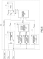
FIG. 5 is a detailed block diagram of the control processor of the power supply unit according to the present disclosure.
FIG. 6A is a waveform designed for the slope of load current and output voltage used in traditional droop current sharing.
FIG. 6B is a waveform designed for the slope of load current and output voltage used in droop current sharing of the present disclosure.
DETAILED DESCRIPTION
Reference will now be made to the drawing figures to describe the present disclosure in detail. It will be understood that the drawing figures and exemplified embodiments of present disclosure are not limited to the details thereof.
The power supply system with dynamic current sharing disclosed in the present disclosure may be applied to, for example, but not limited to, power supplies in related fields such as servers, networking, etc., for example, multiple power supplies connected in parallel are used as a redundant power supply architecture.
Moreover, the present disclosure introduces existing current-sharing technology, including the active current-sharing control, the average current difference compensation control, and the droop current-sharing control, which are integrated/combined to acquire the advantages of each current sharing control, that is, achieving continuous and fast dynamic current sharing for the output current of the load, and increasing voltage compensation speed and current sharing accuracy. Hereinafter, the current-sharing control of the present disclosure will be described in detail.
Please refer to FIG. 2 , which shows a block diagram of a single power supply unit of a power supply system according to the present disclosure. The single power supply unit PSU1-PSUN includes a current detection circuit 101, a detection signal peripheral circuit 102, a digital control processor 103, a current-sharing bus signal peripheral circuit 104, a switch drive circuit 105, and a switched power converter 106. Please refer to FIG. 3 , multiple power supply units are used in parallel as a redundant power supply architecture. In this embodiment, two power supply units PSU1-PSU2 are taken as an example but not for limitation of the present disclosure. In this parallel-connected system, output voltages VOUT of all power supply units PSU1-PSU2 are connected in parallel. The first power supply unit PSU1 provides a first output current Iout1 and the second power supply unit PSU2 provides a second output current Iout2 to commonly provide a total output current Tout total to supply power to a load of the system. In addition, the power supply units PSU1-PSU2 are connected to each other through a current-sharing bus ISB.
Please refer to FIG. 2 again, the current detection circuit 101 is used to detect the output current Tour of the power supply unit PSU (i.e., a load current), and provides a current signal VILOCAL_1 of amplifying the output current IOUT. In practice, the current detection circuit 101 may be, for example, but not limited to, a resistive component, and therefore the output current IOUT flowing through a resistance value R of the resistive component (such as a resistor) generates a voltage difference (Vsense=Iout*R). A differential amplifier circuit composed of OPA may detect the magnitude of the voltage difference (corresponding to the output current IOUT), which represents the amplified current signal VILOCAL_1.
The detection signal peripheral circuit 102 is used to receive three detection signals, including the output voltage VOUT, the current-sharing bus ISB, and the amplified current signal VILOCAL_1 (corresponding to the output current IOUT of the power supply unit). Moreover, the detection signal peripheral circuit 102 adjusts (for example, steps down) the received detection, and provides the adjusted detection signal to the digital control processor 103 to meet the voltage level (magnitude) that the digital control processor 103 can operate. In other words, after processing by the detection signal peripheral circuit 102, the output voltage VOUT is step down (reduced) to VOUT_SENSE, the current signal VILOCAL_1 is step down (reduced) to the second current signal SI21-S12N, and the current-sharing bus signal ISB is step down (reduced) to the first current signal SI1.
The digital control processor 103 digitally filters the second current signal SI2 (i.e., the local current detection signal), and calculates the filtered second current signal SI2 to generate the corresponding current-sharing signal ISHARE to the current-sharing bus signal peripheral circuit 104. The current-sharing bus signal peripheral circuit 104 amplifies the current-sharing signal ISHARE and provides the amplified current-sharing signal ISHARE to the current-sharing bus ISB connected to the current-sharing bus signal peripheral circuit 104. Incidentally, since the current signal on the current-sharing bus ISB is the maximum output current of all power supply units, when all power supply units provide (transmit) the amplified current-sharing signals ISHARE to the current-sharing bus signal peripheral circuit 104, the current-sharing bus ISB reserves the maximum output current as the current signal of the current-sharing bus ISB.
The digital control processor 103 performs an active current-sharing control, an average current difference compensation control, and a droop current-sharing control inside the processor according to the output voltage signal VOUT_SENSE, the second current signal SI21-S12N, and the first current signal SI1 provided by the detection signal peripheral circuit 102 to generate the corresponding reference voltage command and PWM control signal (the detailed description will be made as follows). Therefore, the switch drive circuit 105 is used to control the output voltage VOUT of the switched power converter 106, i.e., the output voltage VOUT of the power supply unit, thereby achieving continuous and fast dynamic current sharing for the output current of the load.
Please refer to FIG. 4 , which shows a block diagram of control processors of the power supply system to perform a dynamic current sharing according to the present disclosure, and also refer to FIG. 3 . The power supply system includes a current-sharing bus ISB and a plurality of a plurality of power supply units PSU1-PSUN. The current-sharing bus ISB provides a first current signal SI1. The power supply units PSU1-PSUN are connected to each other through the current-sharing bus ISB. A digital control processor 103 1-103 N of each power supply unit PSU1-PSUN includes an active current-sharing unit 11, an average current unit 12, a droop current unit 13, and an integration calculation unit 14. A plurality of local current bus ILB1-ILBN correspondingly provide the second current signals SI21-SI2N. That is, a current signal of the output current provided by the local current bus ILB1 of the first power supply unit PSU1 is the first current signal SI21, a current signal of the output current provided by the local current bus ILB2 of the second power supply unit PSU2 is the second current signal SI22, and so on, and the detail description is omitted here for conciseness. The digital control processor 103 receives the output voltage signals VOUT_SENSE1−VOUT_SENSEN, the first current signal Sn, and the second current signals SI21-SI2N provided from the detection signal peripheral circuit 102 shown in FIG. 2 .
As shown in FIG. 4 , the active current-sharing unit 11 of each power supply unit PSU1-PSUN receives the first current signal Sn and the second current signal SI21-SI2N, and compares the second current signal SI21-SI2N with the first current signal Su to generate the compensation voltage VCOMP1-VCOMPN. Specifically, the first power supply unit PSU1 receives the first current signal Sn provided by the current-sharing bus ISB and the second current signal SI21 provided by the first local current bus ILB1. The second power supply unit PSU2 receives the first current signal SI1 provided by the current-sharing bus ISB and the second current signal SI22 provided by the second local current bus ILB2, and so on. The Nth power supply unit PSUN receives the first current signal SI1 provided by the current-sharing bus ISB and the second current signal SI2N provided by the Nth local current bus ILBN. In particular, the magnitude of the first current signal SI1 provided by the shared (commonly-used) current-sharing bus ISB is equal to the maximum value of the second current signals SI21-SI2N. That is, the current signal (i.e., the first current signal SI1) provided by the current-sharing bus ISB corresponds to the maximum output current IOUT of all power supply units PSU1-PSUN.
Please refer to FIG. 5 , which shows a detailed block diagram of the control processor of the power supply unit according to the present disclosure. The active current-sharing unit 11 includes a voltage comparison unit 111 and a compensation unit 112. The voltage comparison unit 111 receives the first current signal Sn and the second current signal SI21-SI2N, and subtracts the second current signal SI21 from the first current signal SI1 (take the first power supply unit PSU1 as an example) so as to acquire/realize a current difference IDIF between the output current IOUT1-IOUTN of each power supply unit PSU1-PSUN and the maximum output current of all power supply units PSU1-PSUN. Furthermore, the compensation unit 112 is used to calculate the current difference IDIF. In one embodiment, the compensation unit 112 may be a digital controller, for example, but not limited to, a proportional-integral (PI) controller to generate the compensation voltages VCOMP1-VCOMPN. Therefore, when the current difference between the first current signal Sn and the second current signal SI21 is larger, the active current-sharing unit 11 provides a larger compensation voltage; otherwise, it provides a smaller compensation voltage. Incidentally, since the first current signal SI1 corresponds to the maximum output current, the aforementioned current value subtraction calculation is the difference acquiring by subtracting the second current signal SI21 from the first current signal Sri.
As shown in FIG. 4 , the average current unit 12 receives the first current signal Su and the second current signal SI21-SI2N, respectively calculates an average value of the first current signal SI1 as a first current average value SHAW; and an average value of the second current signal SI21-SI2N as a second current average value SI21AVG-SI2NAVG, and calculates a difference value between the first current average value SI1AVG and the second current average value SI21AVG-SI2NAVG to generate the average voltage VAVG1-VAVGN.
Specifically, as shown in FIG. 5 , the average current unit 12 includes a first average current calculation unit 121, a second average current calculation unit 122, and an average current difference calculation unit 123. The first average current calculation unit 121 receives the first current signal SI1, and calculates an average value of the first current signal Su as a first current average value SI1AVG. The second average current calculation unit 122 receives the second current signal SI21-SI2N, and calculates an average value of the second current signal SI21-SI2N as a second current average value SI21AVG-SI2NAVG. The average current difference calculation unit 103 receives the first current average value SI1AVG and the second current average value SI21AVG (take the first power supply unit PSU1 as an example), and calculate a difference value between the first current average value SI1AVG and the second current average value SI21AVG to generate the average voltage VAVG1. In particular, the main purpose of average current compensation is to help parallel-connected power supply units to compensate the average voltage error caused by the current detection and the active current-sharing delay in the continuous dynamic load.
As shown in FIG. 4 , the droop current unit 13 receives the second current signal SI21-SI2N to generate the droop compensation voltage VDROOP1-VDROOPN. Specifically, as shown in FIG. 5 , the droop current unit 13 includes a droop function calculation unit 131. The droop function calculation unit 131 receives the second current signal SI21-SI2N to generate the droop compensation voltage VDROOP1-VDROOPN according to the magnitude of the second current signal SI21-SI2N. Please refer to FIG. 6B, the voltage compensation effect is implemented by the local current detection signal of the power supply unit PSU1-PSUN, i.e., the design of the second current signal SI21-SI2N and the droop compensation voltage VDROOP1-VDROOPN. For the droop current unit 13, it only receives the second current signal SI21-SI2N provided by the local current bus ILB1-ILBN, and does not involve the first current signal SI1 of the current sharing bus ISB. Also, according to the built-in (designed) droop slope of the power supply unit PSU1-PSUN itself, the magnitude of the output voltage that changes due to the variation of the load can be adjusted (adjusted). Therefore, the droop current sharing can improve the response speed of dynamic load transient current sharing.
As shown in FIG. 4 , the integration calculation unit 14 receives the compensation voltage VCOMP1-VCOMPN, the average voltage VAVG1-VAVGN, and the droop compensation voltage VDROOP1-VDROOPN. Further, the integration calculation unit 14 generates a reference voltage VOUT_REF1-VOUT_REFN to control the output voltage VOUT_SENSE1-VOUT_SENSEN of the average voltage VAVG1-VAVGN according to the compensation voltage VCOMP1-VCOMPN, the average voltage VAVG1-VAVGN, and the droop compensation voltage VDROOP1-VDROOPN so as to dynamically current share the output currents IOUT1-IOUTN of the power supply units PSU1-PSUN.
Please refer to FIG. 5 , the power supply unit PSU1-PSUN further includes a control signal generation unit 15. The control signal generation unit 15 includes an output voltage comparison unit 151 and a control signal generator 152. Specifically, the reference voltage VOUT_REF1−VOUT_REFN generated from the integration calculation unit 14 and the output voltage VOUT_SENSE1-VOUT_SENSEN of the power supply unit PSU1-PSUN are provided to the output voltage comparison unit 151, and the output voltage comparison unit 151 compares the output voltage VOUT_SENSE1-VOUT_SENSEN with the reference voltage VOUT_REF1-VOUT_REFN (i.e., the voltage subtraction between the output voltage VOUT_SENSE1-VOUT_SENSEN and the reference voltage VOUT_REF1-VOUT_REFN) to acquire an output voltage difference VOUT_DIF. The control signal generator 152 receives the output voltage difference VOUT_DIF to generate a control signal PWM according to the output voltage difference VOUT_DIF, and the control signal PWM is provided to control at least one switch component (not shown) of the switched power converter 106 (shown in FIG. 2 ) through the switch drive circuit 105 so as to control the output voltage VOUT of the switched power converter 106, i.e., the output voltage VOUT of the power supply unit PSU1-PSUN, thereby achieving continuous and fast dynamic current sharing for the output current of the load.
In summary, the present disclosure has the following features and advantages:
-
- 1. The active current-sharing control, the average current difference compensation control, and the droop current-sharing control are integrated/combined to acquire the advantages of each current sharing control, that is, achieving continuous and fast dynamic current sharing for the output current of the load, and increasing voltage compensation speed and current sharing accuracy so that the output currents of the parallel-connected power supply units are approximately equal (for example, the average error between two output currents is less than 5% of the total output current) to implement the optimized current-sharing effect.
- 2. The active current-sharing control is used to increase the output voltage by acquiring the current difference between the current of the current-sharing bus and the current of the local current bus.
- 3. The average current difference compensation control is used to help parallel-connected power supply units to compensate the average voltage error caused by the current detection and the active current-sharing delay in the continuous dynamic load, thereby achieving more accurate current-sharing effect according to the compensated average voltage.
- 4. The droop current-sharing control is used to improve the response speed of dynamic load transient current sharing.
Although the present disclosure has been described with reference to the preferred embodiment thereof, it will be understood that the present disclosure is not limited to the details thereof. Various substitutions and modifications have been suggested in the foregoing description, and others will occur to those of ordinary skill in the art. Therefore, all such substitutions and modifications are intended to be embraced within the scope of the present disclosure as defined in the appended claims.