US11990703B2 - Insulating housing for power terminals and signal terminals - Google Patents

Insulating housing for power terminals and signal terminals Download PDF

Info

Publication number
US11990703B2
US11990703B2 US18/129,102 US202318129102A US11990703B2 US 11990703 B2 US11990703 B2 US 11990703B2 US 202318129102 A US202318129102 A US 202318129102A US 11990703 B2 US11990703 B2 US 11990703B2
Authority
US
United States
Prior art keywords
signal
power
mating
insulating housing
mating portion
Prior art date
Legal status (The legal status is an assumption and is not a legal conclusion. Google has not performed a legal analysis and makes no representation as to the accuracy of the status listed.)
Active
Application number
US18/129,102
Other versions
US20230238730A1 (en
Inventor
Sung-Yu Chen
Current Assignee (The listed assignees may be inaccurate. Google has not performed a legal analysis and makes no representation or warranty as to the accuracy of the list.)
Bellwether Electronic Corp
Original Assignee
Bellwether Electronic Corp
Priority date (The priority date is an assumption and is not a legal conclusion. Google has not performed a legal analysis and makes no representation as to the accuracy of the date listed.)
Filing date
Publication date
Priority claimed from US17/306,961 external-priority patent/US11437746B2/en
Priority claimed from TW111205419U external-priority patent/TWM633994U/en
Application filed by Bellwether Electronic Corp filed Critical Bellwether Electronic Corp
Priority to US18/129,102 priority Critical patent/US11990703B2/en
Publication of US20230238730A1 publication Critical patent/US20230238730A1/en
Assigned to BELLWETHER ELECTRONIC CORP. reassignment BELLWETHER ELECTRONIC CORP. ASSIGNMENT OF ASSIGNORS INTEREST (SEE DOCUMENT FOR DETAILS). Assignors: CHEN, SUNG-YU
Application granted granted Critical
Publication of US11990703B2 publication Critical patent/US11990703B2/en
Active legal-status Critical Current
Anticipated expiration legal-status Critical

Links

Images

Classifications

    • HELECTRICITY
    • H01ELECTRIC ELEMENTS
    • H01RELECTRICALLY-CONDUCTIVE CONNECTIONS; STRUCTURAL ASSOCIATIONS OF A PLURALITY OF MUTUALLY-INSULATED ELECTRICAL CONNECTING ELEMENTS; COUPLING DEVICES; CURRENT COLLECTORS
    • H01R13/00Details of coupling devices of the kinds covered by groups H01R12/70 or H01R24/00 - H01R33/00
    • H01R13/62Means for facilitating engagement or disengagement of coupling parts or for holding them in engagement
    • H01R13/627Snap or like fastening
    • H01R13/6271Latching means integral with the housing
    • H01R13/6272Latching means integral with the housing comprising a single latching arm
    • HELECTRICITY
    • H01ELECTRIC ELEMENTS
    • H01RELECTRICALLY-CONDUCTIVE CONNECTIONS; STRUCTURAL ASSOCIATIONS OF A PLURALITY OF MUTUALLY-INSULATED ELECTRICAL CONNECTING ELEMENTS; COUPLING DEVICES; CURRENT COLLECTORS
    • H01R13/00Details of coupling devices of the kinds covered by groups H01R12/70 or H01R24/00 - H01R33/00
    • H01R13/46Bases; Cases
    • H01R13/502Bases; Cases composed of different pieces
    • H01R13/504Bases; Cases composed of different pieces different pieces being moulded, cemented, welded, e.g. ultrasonic, or swaged together
    • H01R13/5045Bases; Cases composed of different pieces different pieces being moulded, cemented, welded, e.g. ultrasonic, or swaged together different pieces being assembled by press-fit
    • HELECTRICITY
    • H01ELECTRIC ELEMENTS
    • H01RELECTRICALLY-CONDUCTIVE CONNECTIONS; STRUCTURAL ASSOCIATIONS OF A PLURALITY OF MUTUALLY-INSULATED ELECTRICAL CONNECTING ELEMENTS; COUPLING DEVICES; CURRENT COLLECTORS
    • H01R13/00Details of coupling devices of the kinds covered by groups H01R12/70 or H01R24/00 - H01R33/00
    • H01R13/40Securing contact members in or to a base or case; Insulating of contact members
    • H01R13/42Securing in a demountable manner
    • H01R13/422Securing in resilient one-piece base or case, e.g. by friction; One-piece base or case formed with resilient locking means
    • H01R13/4223Securing in resilient one-piece base or case, e.g. by friction; One-piece base or case formed with resilient locking means comprising integral flexible contact retaining fingers
    • HELECTRICITY
    • H01ELECTRIC ELEMENTS
    • H01RELECTRICALLY-CONDUCTIVE CONNECTIONS; STRUCTURAL ASSOCIATIONS OF A PLURALITY OF MUTUALLY-INSULATED ELECTRICAL CONNECTING ELEMENTS; COUPLING DEVICES; CURRENT COLLECTORS
    • H01R12/00Structural associations of a plurality of mutually-insulated electrical connecting elements, specially adapted for printed circuits, e.g. printed circuit boards [PCB], flat or ribbon cables, or like generally planar structures, e.g. terminal strips, terminal blocks; Coupling devices specially adapted for printed circuits, flat or ribbon cables, or like generally planar structures; Terminals specially adapted for contact with, or insertion into, printed circuits, flat or ribbon cables, or like generally planar structures
    • H01R12/70Coupling devices
    • H01R12/71Coupling devices for rigid printing circuits or like structures
    • H01R12/72Coupling devices for rigid printing circuits or like structures coupling with the edge of the rigid printed circuits or like structures
    • H01R12/722Coupling devices for rigid printing circuits or like structures coupling with the edge of the rigid printed circuits or like structures coupling devices mounted on the edge of the printed circuits
    • H01R12/724Coupling devices for rigid printing circuits or like structures coupling with the edge of the rigid printed circuits or like structures coupling devices mounted on the edge of the printed circuits containing contact members forming a right angle
    • HELECTRICITY
    • H01ELECTRIC ELEMENTS
    • H01RELECTRICALLY-CONDUCTIVE CONNECTIONS; STRUCTURAL ASSOCIATIONS OF A PLURALITY OF MUTUALLY-INSULATED ELECTRICAL CONNECTING ELEMENTS; COUPLING DEVICES; CURRENT COLLECTORS
    • H01R2107/00Four or more poles

Definitions

  • the present disclosure relates to an insulating housing and an electrical connector, and more particularly to an insulating housing and an electrical connector that have a power portion and a signal portion.
  • wire-to-board connectors are conventionally designed to have separate connections, in which a power connector and a signal connector are respectively used for connection and transmission.
  • the power connector is connected to a power wire
  • the signal connector is connected to a plurality of signal wires.
  • a conventional connection process for transmitting power and signal separately is complicated and takes up space, which does not match the recent trend of miniaturization and is time-consuming.
  • the present disclosure provides an insulating housing and an electrical connecter. Also included herein is a connection manner for transmission of power and signal.
  • the present disclosure provides an insulating housing for an electrical connecter.
  • the insulating housing comprises a body portion, a power mating portion, and a signal mating portion.
  • the power mating portion has a plurality of column bodies extending from a front surface thereof.
  • the signal mating portion is connected with the body portion and located over one side of the power mating portion.
  • the present disclosure provides an electrical connector.
  • the electrical connector for transmitting power and signal with a mating electrical connector, comprises a body portion, a plurality of power terminals, a power mating portion, at least one signal terminal, and a signal mating portion.
  • the power mating portion has a plurality of column bodies extending from a front surface thereof and accommodating the plurality of power terminals therein.
  • the signal mating portion is connected with the body portion and located over one side of the power mating portion and accommodating at least one signal terminal.
  • the present disclosure provides an insulating housing for an electrical connecter.
  • the insulating housing comprises a power mating portion and a signal mating portion.
  • the power mating portion has a plurality of power sockets.
  • the signal mating portion is located on one side of the power mating portion and has a signal socket. Wherein, the signal socket and at least one power socket have a common wall there between.
  • the present disclosure provides an electrical connector for transmitting power and signal with a mating electrical connector.
  • the electrical connector comprises a plurality of power terminals, a power mating portion, at least one signal terminal, and a signal mating portion.
  • the power mating portion has a plurality of power sockets accommodating the plurality of power terminals therein.
  • the signal mating portion is located on one side of the power mating portion and has a signal socket accommodating at least one signal terminal. Wherein, the signal socket and at least one power socket have a common wall there between.
  • the insulating housing and the electrical connector provided by the present disclosure utilizes the connection manners for combined transmission of power and signal, thereby allowing the mating process to be simplified and saving space to match the current trend of miniaturization.
  • FIG. 1 is a perspective view of an insulating housing according to a first embodiment of the present disclosure
  • FIG. 2 is another perspective view of the insulating housing according to the first embodiment of the present disclosure
  • FIG. 3 is side view of the insulating housing according to the first embodiment of the present disclosure
  • FIG. 4 is a schematic view of a wire-end connector and a board-end connector according to the first embodiment of the present disclosure
  • FIG. 5 is an assembly view of the wire-end connector and the board-end connector according to the first embodiment of the present disclosure
  • FIG. 6 is a front view of an insulating housing according to a second embodiment of the present disclosure.
  • FIG. 7 is a perspective view of an insulating housing according to a third embodiment of the present disclosure.
  • FIG. 8 is another perspective view of the insulating housing according to the third embodiment of the present disclosure.
  • FIG. 9 is a perspective view of an insulating housing according to a fourth embodiment of the present disclosure.
  • FIG. 10 is another perspective view of the insulating housing according to the fourth embodiment of the present disclosure.
  • Numbering terms such as “first”, “second” or “third” can be used to describe various components, signals or the like, which are for distinguishing one component/signal from another one only, and are not intended to, nor should be construed to impose any substantive limitations on the components, signals or the like.
  • FIG. 1 is a perspective view of an insulating housing according to a first embodiment of the present disclosure
  • FIG. 2 is another perspective view of the insulating housing according to the first embodiment of the present disclosure
  • FIG. 3 is a side view of the insulating housing according to the first embodiment of the present disclosure.
  • the first embodiment of the present disclosure provides an insulating housing A for wire-end connectors, and the insulating housing A includes a body portion 1 , a power mating portion 2 , a signal mating portion 3 , and a snap-fit member 4 .
  • the body portion 1 has a first surface 11 , a second surface 12 , a third surface 13 , and a fourth surface 14 .
  • the first surface 11 is disposed opposite to the second surface 12
  • the third surface 13 is disposed opposite to the fourth surface 14
  • the first surface 11 and the second surface 12 are connected between the third surface 13 and the fourth surface 14 .
  • a plurality of first channels 10 are formed inside the body portion 1 in a first direction (Y-axis direction).
  • the plurality of first channels 10 are arranged in at least one row, and the plurality of first channels 10 are exemplified as being arranged in two horizontal and parallel rows in this embodiment.
  • the power mating portion 2 is disposed on the second surface 12 on one side of the body portion 1 .
  • the power mating portion 2 includes a plurality of column bodies 21 that are in horizontal and parallel arrangements.
  • Each of the plurality of column bodies 21 has a first end 211 and a second end 212 .
  • the first end 211 is connected to the second surface 12 .
  • the plurality of first channels 10 respectively penetrate the plurality of column bodies 21 , and in each of the first channels 10 , two first openings 101 are formed on the first surface 11 and the second end 212 of a corresponding one of the column bodies 21 , respectively.
  • the signal mating portion 3 is disposed on the third surface 13 , and the signal mating portion 3 has a fifth surface 31 and a sixth surface 32 disposed opposite to each other.
  • a plurality of second channels 30 are formed inside the signal mating portion 3 in the first direction, and in each of the second channels 30 , two second openings 301 are formed on the fifth surface 31 and the sixth surface 32 , respectively.
  • the sixth surface 32 of the signal mating portion 3 is a mating interface for mating with a signal mating socket B 3 (referring to FIG. 4 ).
  • the mating interface may be a square interface. Two sides of the portion of the signal mating portion 3 connected to the third surface 13 can further respectively have two support portions 33 formed thereon to enhance the structural strength.
  • the snap-fit member 4 is disposed on the fourth surface 14 .
  • the snap-fit member 4 includes a press portion 41 and a snap-fit portion 42 . Further, the snap-fit member 4 also includes a connection portion 43 .
  • the connection portion 43 is connected to the fourth surface 14 .
  • the press portion 41 is located on a rear side of a junction 431 between the connection portion 43 and the fourth surface 14 (i.e., a side of the snap-fit member 4 that extends in the negative Y-axis direction).
  • the snap-fit portion 42 is located on a front side of the junction 431 (i.e., a side of the snap-fit member 4 that extends in the positive Y-axis direction) between the connection portion 43 and the fourth surface 14 .
  • a projection area of the press portion 41 projected onto the fourth surface 14 (or the third surface 13 ) at least partially overlaps with a projection area of the signal mating portion 3 projected onto the fourth surface 14 .
  • a length of an overlapping projection area of the press portion 41 and the signal mating portion 3 projected onto the fourth surface 14 (or the third surface 13 ) in the first direction is equal to or greater than half of a length of the projection area of the press portion 41 projected onto the fourth surface 14 in the first direction.
  • the press portion 41 includes a convex portion 411 , and the convex portion 411 has an inclined surface 41 A and a horizontal surface 41 B.
  • the convex portion 411 is a protruding portion formed on one side of the snap-fit member 4 near the first surface.
  • a projection area of the convex portion 411 projected onto the fourth surface 14 at least partially overlaps with a projection area of the signal mating portion 3 projected onto the fourth surface 14 .
  • the inclined surface 41 A of the convex portion 411 overlaps with the projection area of the signal mating portion 3 projected onto the fourth surface 14 .
  • both the inclined surface 41 A and the horizontal surface 41 B of the convex portion 411 overlap with the projection area of the signal mating portion 3 projected onto the fourth surface 14 .
  • the first surface 11 and the fifth surface 31 are spaced apart by a first horizontal distance H 1 in the first direction, and a junction between the inclined surface 41 A and the horizontal surface 41 B of the press portion 41 is spaced apart from the first surface 11 in a second horizontal distance H 2 in the first direction.
  • the first horizontal distance H 1 is equal to or smaller than the second horizontal distance H 2 .
  • a fillet is formed at a junction between the first surface 11 and the third surface 13 , that is, an edge corner of the body portion 1 near the signal mating portion 3 is rounded.
  • the fillet has a radius of curvature R between 0.5 mm and 0.8 mm.
  • FIG. 4 is a schematic view of a wire-end connector and a board-end connector according to the first embodiment of the present disclosure
  • FIG. 5 is an assembly view of the wire-end connector and the board-end connector according to the first embodiment of the present disclosure.
  • the present disclosure further provides a wire-end connector M, and the wire-end connector M includes the above-mentioned insulating housing A, a plurality of power wire-end terminals, and a plurality of signal wire-end terminals.
  • the plurality of power wire-end terminals are inserted into (the plurality of first channels 10 of) the body portion 1 and the power mating portion 2 through the plurality of first openings 101 of the first surface 11 , respectively.
  • a plurality of signal wire-end terminals are inserted into the signal mating portion 3 .
  • the plurality of signal wire-end terminals are inserted into (the plurality of second channels 30 of) the signal mating portion 3 through the plurality of second openings 301 of the fifth surface 31 , respectively.
  • the power mating portion 2 of the wire-end connector M is mated into a plurality of power mating sockets B 2 of the board-end connector B through the plurality of column bodies 21 of the power mating portion 2 , and power board-end terminals (not shown in the drawings) in the power mating sockets B 2 are in electrical contact with the plurality of power wire-end terminals through the first opening 101 of the second end 212 of each of the column bodies 21 .
  • the signal mating portion 3 of the wire-end connector M is inserted in the signal mating socket B 3 of the board-end connector B through the signal mating portion 3 , and a plurality of signal board-end terminals (not shown in the drawings) in the signal mating socket B 3 are in electrical contact with a plurality of signal wire-end terminals by being inserted in the plurality of second channels 30 through the plurality of second openings 301 of the sixth surface 32 of the signal mating portion 3 .
  • the plurality of signal board-end terminals may transmit at least a portion of the following signals to the plurality of signal wire-end terminals, said signals indicating the following information: power supply status, voltage status, maximum power supply value, overcurrent protection, over temperature protection, emergency termination of power supply, etc.
  • the wire-end connector M is electrically connected to the circuit board C that is connected to the board-end connector B by being assembled to the board-end connector B.
  • one of the second channels 30 can be filled so as to be used as a fool-proof device in the present disclosure.
  • the plurality of signal board-end terminals have two or more different terminal spacings (pitches) therebetween to provide a fool-proof effect.
  • the inclined surface 41 A of the press portion 41 overlaps with a projection area of the signal mating portion 3 projected onto the fourth surface 14 , and the first horizontal distance H 1 is smaller than the second horizontal distance H 2 . Therefore, when the user takes the wire-end connector M, fingers of the user can be in contact with the press portion 41 and the signal mating portion 3 at two sides of the insulating housing A, respectively. The finger of a user will press on a position of the signal mating portion 3 instead of pressing the signal wire (not shown in the drawings).
  • the signal wire is subjected to a smaller cross-cutting force at the junction so as to avoid being broken or damaged.
  • one side of the body portion 1 is flush with one side of the signal mating portion 3 (i.e., the first surface 11 is flush with the fifth surface 31 ), that is, the first horizontal distance H 1 is equal to 0.
  • the fingers of the user can press on the position of the signal mating portion 3 instead of pressing the signal wire, so that there is no need to worry about the signal wire being broken by the cross-cutting force exerted by the edge corners of the body portion 1 .
  • FIG. 6 is a front view of an insulating housing according to a second embodiment of the present disclosure.
  • the insulating housing A provided in this embodiment has a similar structure compared with the insulating housing A provided in the first embodiment, and the similarities therebetween are not repeated.
  • the difference between the insulating housing A of this embodiment and the insulating housing A of the first embodiment resides in that, the signal mating portion 3 of the insulating housing A has two rows of the second channels 30 in an upper and a lower arrangement. That is, the signal mating portion 3 of the insulating housing A has the plurality of second channels 30 in a horizontal and parallel arrangement, while the signal mating portion 3 of the insulating housing A of the first embodiment has only one row of the second channels 30 .
  • this disclosure is not limited by a number of the second channels 30 .
  • FIG. 7 is a perspective view of an insulating housing according to a third embodiment of the present disclosure
  • FIG. 8 is another perspective view of the insulating housing according to the third embodiment of the present disclosure.
  • the insulating housing A provided in this embodiment has a similar structure compared with the insulating housing A provided in the first embodiment, and the similarities therebetween are not repeated.
  • the difference between the insulating housing A of this embodiment and the insulating housing A of the first embodiment resides in that, the snap-fit member 4 has a different shape and the first surface 11 has a plurality of recesses 111 .
  • the snap-fit member 4 also includes a fan-shaped portion 44 , and the fan-shaped portion 44 is connected between the snap-fit portion 42 and the press portion 41 . More precisely, the fan-shaped portion 44 is the part of the snap-fit member 4 having a variable width between the snap-fit portion 42 and the press portion 41 .
  • the press portion 41 has a first width W 1 and the snap-fit portion 42 has a second width W 2 , and the first width W 1 is at least 1.5 times the second width W 2 .
  • the first width W 1 is equal to or greater than 6 mm.
  • the design of the first width W 1 being at least 1.5 times the second width W 2 , a surface area of a surface for being pressed on the snap-fit member 4 is widened to facilitate the application of force by the user.
  • the plurality of recesses 111 are formed at positions on the third surface 13 that correspond to positions of the second openings 301 on the fifth surface 31 (i.e., the edge corner of the body portion 1 near the signal mating portion 3 corresponding to the positions of the plurality of signal wire-end terminals), and the plurality of recesses 111 can accommodate the wires of the signal wire-end terminal that extend from the second channels 30 of the signal mating portion 3 .
  • FIG. 9 is a perspective view of an insulating housing according to a fourth embodiment of the present disclosure
  • FIG. 10 is another perspective view of the insulating housing according to the fourth embodiment of the present disclosure.
  • the insulating housing A provided in this embodiment has a similar structure compared with the insulating housing A provided in the third embodiment, and the similarities therebetween are not repeated.
  • the difference between the insulating housing A of this embodiment and the insulating housing A of the third embodiment resides in that, the press portion 41 further includes a convex portion 411 , and the convex portion 411 is formed on an upper surface of the press portion 41 .
  • a projection area of the convex portion 411 projected onto the fourth surface 14 at least partially overlaps with the projection area of the signal mating portion 3 projected onto the fourth surface 14 .
  • one of the beneficial effects of the present disclosure is that, in the insulating housing A and the wire-end connector M provided by the present disclosure, by virtue of the projection area of the press portion 41 projected onto the surface of the body portion 1 at least partially being overlapped with the projection area of the signal mating portion 3 projected onto the surface of the body portion 1 , the issue of a user inadvertently pressing on a signal wire at sides of a housing when mating/demating a wire-end connector M to a board-end connector B and causing the signal wire to be bent or loosened can be avoided.
  • the insulating housing A and the wire-end connector M provided by the present disclosure, by the design of the first horizontal distance H 1 being smaller than the second horizontal distance H 2 , and a fillet being formed at the junction between the first surface 11 and the third surface 13 , when the user takes the wire-end connector M, fingers of the user can be in contact with the press portion 41 and the signal mating portion 3 at two sides of the insulating housing A, respectively. The finger of a user will press on a position of the signal mating portion 3 instead of pressing on the signal wire (not shown in the drawings).
  • the signal wire is subjected to a smaller cross-cutting force at the junction and avoids being broken.

Landscapes

  • Details Of Connecting Devices For Male And Female Coupling (AREA)
  • Coupling Device And Connection With Printed Circuit (AREA)

Abstract

An insulating housing and an electrical connector including the insulating housing are provided. The electrical connector, for transmitting power and signal with a mating electrical connector, comprises a body portion, a plurality of power terminals, a power mating portion, at least one signal terminal, and a signal mating portion. The power mating portion has a plurality of column bodies extending from a front surface thereof and accommodating the plurality of power terminals therein. The signal mating portion is connected with the body portion and located over one side of the power mating portion and accommodating at least one signal terminal.

Description

CROSS-REFERENCE TO RELATED PATENT APPLICATION
This application is a Continuation Application of the U.S. application Ser. No. 17/870,845, filed on Jul. 22, 2022 and entitled “INSULATING HOUSING AND WIRE-END CONNECTOR”.
This application claims the benefit of priority to Taiwan Patent Application No. 111205419, filed on May 25, 2022. The entire content of the above identified application is incorporated herein by reference.
This application claims the benefit of priority to the U.S. Provisional Patent Application Ser. No. 63/020,551 filed on May 6, 2020, which application is incorporated herein by reference in its entirety.
Some references, which may include patents, patent applications and various publications, may be cited and discussed in the description of this disclosure. The citation and/or discussion of such references is provided merely to clarify the description of the present disclosure and is not an admission that any such reference is “prior art” to the disclosure described herein. All references cited and discussed in this specification are incorporated herein by reference in their entireties and to the same extent as if each reference was individually incorporated by reference.
FIELD OF THE DISCLOSURE
The present disclosure relates to an insulating housing and an electrical connector, and more particularly to an insulating housing and an electrical connector that have a power portion and a signal portion.
BACKGROUND OF THE DISCLOSURE
Electronic products have developed toward miniaturization, resulting in limited space in the electronic products.
For electronic components that are required to be connected to power wires and signal wires (e.g., control signal wires, or detection signal wires, etc.), wire-to-board connectors are conventionally designed to have separate connections, in which a power connector and a signal connector are respectively used for connection and transmission. The power connector is connected to a power wire, and the signal connector is connected to a plurality of signal wires.
A conventional connection process for transmitting power and signal separately is complicated and takes up space, which does not match the recent trend of miniaturization and is time-consuming.
Therefore, how to improve the structural design to allow the wire-to-board connectors to conform to the trend of miniaturization, so as to overcome the above-mentioned deficiencies, has become an issue to be addressed in this technological field.
SUMMARY OF THE DISCLOSURE
In response to the above-referenced technical inadequacy, the present disclosure provides an insulating housing and an electrical connecter. Also included herein is a connection manner for transmission of power and signal.
In one aspect, the present disclosure provides an insulating housing for an electrical connecter. The insulating housing comprises a body portion, a power mating portion, and a signal mating portion. The power mating portion has a plurality of column bodies extending from a front surface thereof. The signal mating portion is connected with the body portion and located over one side of the power mating portion.
In another aspect, the present disclosure provides an electrical connector. The electrical connector, for transmitting power and signal with a mating electrical connector, comprises a body portion, a plurality of power terminals, a power mating portion, at least one signal terminal, and a signal mating portion. The power mating portion has a plurality of column bodies extending from a front surface thereof and accommodating the plurality of power terminals therein. The signal mating portion is connected with the body portion and located over one side of the power mating portion and accommodating at least one signal terminal.
In yet another aspect, the present disclosure provides an insulating housing for an electrical connecter. The insulating housing comprises a power mating portion and a signal mating portion. The power mating portion has a plurality of power sockets. The signal mating portion is located on one side of the power mating portion and has a signal socket. Wherein, the signal socket and at least one power socket have a common wall there between.
In still another aspect, the present disclosure provides an electrical connector for transmitting power and signal with a mating electrical connector. The electrical connector comprises a plurality of power terminals, a power mating portion, at least one signal terminal, and a signal mating portion. The power mating portion has a plurality of power sockets accommodating the plurality of power terminals therein. The signal mating portion is located on one side of the power mating portion and has a signal socket accommodating at least one signal terminal. Wherein, the signal socket and at least one power socket have a common wall there between.
Therefore, one of the advantageous effects of the present disclosure is that, the insulating housing and the electrical connector provided by the present disclosure utilizes the connection manners for combined transmission of power and signal, thereby allowing the mating process to be simplified and saving space to match the current trend of miniaturization.
These and other aspects of the present disclosure will become apparent from the following description of the embodiment taken in conjunction with the following drawings and their captions, although variations and modifications therein may be affected without departing from the spirit and scope of the novel concepts of the disclosure.
BRIEF DESCRIPTION OF THE DRAWINGS
The described embodiments may be better understood by reference to the following description and the accompanying drawings, in which:
FIG. 1 is a perspective view of an insulating housing according to a first embodiment of the present disclosure;
FIG. 2 is another perspective view of the insulating housing according to the first embodiment of the present disclosure;
FIG. 3 is side view of the insulating housing according to the first embodiment of the present disclosure;
FIG. 4 is a schematic view of a wire-end connector and a board-end connector according to the first embodiment of the present disclosure;
FIG. 5 is an assembly view of the wire-end connector and the board-end connector according to the first embodiment of the present disclosure;
FIG. 6 is a front view of an insulating housing according to a second embodiment of the present disclosure;
FIG. 7 is a perspective view of an insulating housing according to a third embodiment of the present disclosure;
FIG. 8 is another perspective view of the insulating housing according to the third embodiment of the present disclosure;
FIG. 9 is a perspective view of an insulating housing according to a fourth embodiment of the present disclosure; and
FIG. 10 is another perspective view of the insulating housing according to the fourth embodiment of the present disclosure.
DETAILED DESCRIPTION OF THE EXEMPLARY EMBODIMENTS
The present disclosure is more particularly described in the following examples that are intended as illustrative only since numerous modifications and variations therein will be apparent to those skilled in the art. Like numbers in the drawings indicate like components throughout the views. As used in the description herein and throughout the claims that follow, unless the context clearly dictates otherwise, the meaning of “a”, “an”, and “the” includes plural reference, and the meaning of “in” includes “in” and “on”. Titles or subtitles can be used herein for the convenience of a reader, which shall have no influence on the scope of the present disclosure.
The terms used herein generally have their ordinary meanings in the art. In the case of conflict, the present document, including any definitions given herein, will prevail. The same thing can be expressed in more than one way. Alternative language and synonyms can be used for any term(s) discussed herein, and no special significance is to be placed upon whether a term is elaborated or discussed herein. A recital of one or more synonyms does not exclude the use of other synonyms. The use of examples anywhere in this specification including examples of any terms is illustrative only, and in no way limits the scope and meaning of the present disclosure or of any exemplified term. Likewise, the present disclosure is not limited to various embodiments given herein. Numbering terms such as “first”, “second” or “third” can be used to describe various components, signals or the like, which are for distinguishing one component/signal from another one only, and are not intended to, nor should be construed to impose any substantive limitations on the components, signals or the like.
First Embodiment
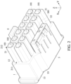
Reference is made to FIGS. 1 to 3 . FIG. 1 is a perspective view of an insulating housing according to a first embodiment of the present disclosure, FIG. 2 is another perspective view of the insulating housing according to the first embodiment of the present disclosure, and FIG. 3 is a side view of the insulating housing according to the first embodiment of the present disclosure. The first embodiment of the present disclosure provides an insulating housing A for wire-end connectors, and the insulating housing A includes a body portion 1, a power mating portion 2, a signal mating portion 3, and a snap-fit member 4.
The body portion 1 has a first surface 11, a second surface 12, a third surface 13, and a fourth surface 14. The first surface 11 is disposed opposite to the second surface 12, the third surface 13 is disposed opposite to the fourth surface 14, and the first surface 11 and the second surface 12 are connected between the third surface 13 and the fourth surface 14. A plurality of first channels 10 are formed inside the body portion 1 in a first direction (Y-axis direction). The plurality of first channels 10 are arranged in at least one row, and the plurality of first channels 10 are exemplified as being arranged in two horizontal and parallel rows in this embodiment.
The power mating portion 2 is disposed on the second surface 12 on one side of the body portion 1. The power mating portion 2 includes a plurality of column bodies 21 that are in horizontal and parallel arrangements. Each of the plurality of column bodies 21 has a first end 211 and a second end 212. The first end 211 is connected to the second surface 12. Because the plurality of column bodies 21 are connected to the body portion 1, the plurality of first channels 10 respectively penetrate the plurality of column bodies 21, and in each of the first channels 10, two first openings 101 are formed on the first surface 11 and the second end 212 of a corresponding one of the column bodies 21, respectively.
The signal mating portion 3 is disposed on the third surface 13, and the signal mating portion 3 has a fifth surface 31 and a sixth surface 32 disposed opposite to each other. A plurality of second channels 30 are formed inside the signal mating portion 3 in the first direction, and in each of the second channels 30, two second openings 301 are formed on the fifth surface 31 and the sixth surface 32, respectively. The sixth surface 32 of the signal mating portion 3 is a mating interface for mating with a signal mating socket B3 (referring to FIG. 4 ). The mating interface may be a square interface. Two sides of the portion of the signal mating portion 3 connected to the third surface 13 can further respectively have two support portions 33 formed thereon to enhance the structural strength. Since each of the support portions 33 is a beveled surface, the fifth surface 31 is trapezoidal when viewed from the positive Y-axis of FIG. 1 . The snap-fit member 4 is disposed on the fourth surface 14. The snap-fit member 4 includes a press portion 41 and a snap-fit portion 42. Further, the snap-fit member 4 also includes a connection portion 43. The connection portion 43 is connected to the fourth surface 14. The press portion 41 is located on a rear side of a junction 431 between the connection portion 43 and the fourth surface 14 (i.e., a side of the snap-fit member 4 that extends in the negative Y-axis direction). The snap-fit portion 42 is located on a front side of the junction 431 (i.e., a side of the snap-fit member 4 that extends in the positive Y-axis direction) between the connection portion 43 and the fourth surface 14. A projection area of the press portion 41 projected onto the fourth surface 14 (or the third surface 13) at least partially overlaps with a projection area of the signal mating portion 3 projected onto the fourth surface 14. Preferably, a length of an overlapping projection area of the press portion 41 and the signal mating portion 3 projected onto the fourth surface 14 (or the third surface 13) in the first direction is equal to or greater than half of a length of the projection area of the press portion 41 projected onto the fourth surface 14 in the first direction.
Furthermore, the press portion 41 includes a convex portion 411, and the convex portion 411 has an inclined surface 41A and a horizontal surface 41B. Mainly, the convex portion 411 is a protruding portion formed on one side of the snap-fit member 4 near the first surface. As seen in FIG. 3 , a projection area of the convex portion 411 projected onto the fourth surface 14 at least partially overlaps with a projection area of the signal mating portion 3 projected onto the fourth surface 14. More precisely, the inclined surface 41A of the convex portion 411 overlaps with the projection area of the signal mating portion 3 projected onto the fourth surface 14. Preferably, both the inclined surface 41A and the horizontal surface 41B of the convex portion 411 overlap with the projection area of the signal mating portion 3 projected onto the fourth surface 14.
Referring to FIGS. 1 to 3 , in this embodiment, the first surface 11 and the fifth surface 31 are spaced apart by a first horizontal distance H1 in the first direction, and a junction between the inclined surface 41A and the horizontal surface 41B of the press portion 41 is spaced apart from the first surface 11 in a second horizontal distance H2 in the first direction. The first horizontal distance H1 is equal to or smaller than the second horizontal distance H2. Further, a fillet is formed at a junction between the first surface 11 and the third surface 13, that is, an edge corner of the body portion 1 near the signal mating portion 3 is rounded. Preferably, the fillet has a radius of curvature R between 0.5 mm and 0.8 mm.
Reference is made to FIG. 2 , FIG. 4 , and FIG. 5 . FIG. 4 is a schematic view of a wire-end connector and a board-end connector according to the first embodiment of the present disclosure, and FIG. 5 is an assembly view of the wire-end connector and the board-end connector according to the first embodiment of the present disclosure. The present disclosure further provides a wire-end connector M, and the wire-end connector M includes the above-mentioned insulating housing A, a plurality of power wire-end terminals, and a plurality of signal wire-end terminals. The plurality of power wire-end terminals are inserted into (the plurality of first channels 10 of) the body portion 1 and the power mating portion 2 through the plurality of first openings 101 of the first surface 11, respectively. A plurality of signal wire-end terminals are inserted into the signal mating portion 3. In the embodiment, the plurality of signal wire-end terminals are inserted into (the plurality of second channels 30 of) the signal mating portion 3 through the plurality of second openings 301 of the fifth surface 31, respectively. When the wire-end connector M is assembled with the board-end connector B, a hook B1 of the board-end connector B will engage to the snap-fit portion 42 of the wire-end connector M. The power mating portion 2 of the wire-end connector M is mated into a plurality of power mating sockets B2 of the board-end connector B through the plurality of column bodies 21 of the power mating portion 2, and power board-end terminals (not shown in the drawings) in the power mating sockets B2 are in electrical contact with the plurality of power wire-end terminals through the first opening 101 of the second end 212 of each of the column bodies 21. Similarly, when the wire-end connector M is assembled with the board-end connector B, the signal mating portion 3 of the wire-end connector M is inserted in the signal mating socket B3 of the board-end connector B through the signal mating portion 3, and a plurality of signal board-end terminals (not shown in the drawings) in the signal mating socket B3 are in electrical contact with a plurality of signal wire-end terminals by being inserted in the plurality of second channels 30 through the plurality of second openings 301 of the sixth surface 32 of the signal mating portion 3. Therefore, the plurality of signal board-end terminals may transmit at least a portion of the following signals to the plurality of signal wire-end terminals, said signals indicating the following information: power supply status, voltage status, maximum power supply value, overcurrent protection, over temperature protection, emergency termination of power supply, etc. Then, the wire-end connector M is electrically connected to the circuit board C that is connected to the board-end connector B by being assembled to the board-end connector B. It is worth mentioning that, as shown in FIG. 1 and FIG. 2 , one of the second channels 30 can be filled so as to be used as a fool-proof device in the present disclosure. In other words, the plurality of signal board-end terminals have two or more different terminal spacings (pitches) therebetween to provide a fool-proof effect.
As mentioned above, when the wire-end connector M and the board-end connector B are assembled or separated, the inclined surface 41A of the press portion 41 overlaps with a projection area of the signal mating portion 3 projected onto the fourth surface 14, and the first horizontal distance H1 is smaller than the second horizontal distance H2. Therefore, when the user takes the wire-end connector M, fingers of the user can be in contact with the press portion 41 and the signal mating portion 3 at two sides of the insulating housing A, respectively. The finger of a user will press on a position of the signal mating portion 3 instead of pressing the signal wire (not shown in the drawings). In addition, even if the user inadvertently presses the signal wire, since a fillet is formed at the junction between the first surface 11 and the third surface 13, that is, an edge corner of the body portion 1 near the signal mating portion 3 is rounded, the signal wire is subjected to a smaller cross-cutting force at the junction so as to avoid being broken or damaged.
It is worth mentioning that, in other embodiments, one side of the body portion 1 is flush with one side of the signal mating portion 3 (i.e., the first surface 11 is flush with the fifth surface 31), that is, the first horizontal distance H1 is equal to 0. In this case, when the user takes the wire-end connector M in hand, the fingers of the user can press on the position of the signal mating portion 3 instead of pressing the signal wire, so that there is no need to worry about the signal wire being broken by the cross-cutting force exerted by the edge corners of the body portion 1.
Second Embodiment
Reference is made to FIG. 6 . FIG. 6 is a front view of an insulating housing according to a second embodiment of the present disclosure. The insulating housing A provided in this embodiment has a similar structure compared with the insulating housing A provided in the first embodiment, and the similarities therebetween are not repeated. The difference between the insulating housing A of this embodiment and the insulating housing A of the first embodiment resides in that, the signal mating portion 3 of the insulating housing A has two rows of the second channels 30 in an upper and a lower arrangement. That is, the signal mating portion 3 of the insulating housing A has the plurality of second channels 30 in a horizontal and parallel arrangement, while the signal mating portion 3 of the insulating housing A of the first embodiment has only one row of the second channels 30. However, this disclosure is not limited by a number of the second channels 30.
Third Embodiment
Reference is made to FIG. 7 and FIG. 8 . FIG. 7 is a perspective view of an insulating housing according to a third embodiment of the present disclosure, and FIG. 8 is another perspective view of the insulating housing according to the third embodiment of the present disclosure. The insulating housing A provided in this embodiment has a similar structure compared with the insulating housing A provided in the first embodiment, and the similarities therebetween are not repeated. The difference between the insulating housing A of this embodiment and the insulating housing A of the first embodiment resides in that, the snap-fit member 4 has a different shape and the first surface 11 has a plurality of recesses 111. In this embodiment, the snap-fit member 4 also includes a fan-shaped portion 44, and the fan-shaped portion 44 is connected between the snap-fit portion 42 and the press portion 41. More precisely, the fan-shaped portion 44 is the part of the snap-fit member 4 having a variable width between the snap-fit portion 42 and the press portion 41. The press portion 41 has a first width W1 and the snap-fit portion 42 has a second width W2, and the first width W1 is at least 1.5 times the second width W2. Preferably, the first width W1 is equal to or greater than 6 mm. In the present disclosure, by the design of the first width W1 being at least 1.5 times the second width W2, a surface area of a surface for being pressed on the snap-fit member 4 is widened to facilitate the application of force by the user. The plurality of recesses 111 are formed at positions on the third surface 13 that correspond to positions of the second openings 301 on the fifth surface 31 (i.e., the edge corner of the body portion 1 near the signal mating portion 3 corresponding to the positions of the plurality of signal wire-end terminals), and the plurality of recesses 111 can accommodate the wires of the signal wire-end terminal that extend from the second channels 30 of the signal mating portion 3.
Fourth Embodiment
Reference is made to FIG. 9 and FIG. 10 . FIG. 9 is a perspective view of an insulating housing according to a fourth embodiment of the present disclosure, and FIG. 10 is another perspective view of the insulating housing according to the fourth embodiment of the present disclosure. The insulating housing A provided in this embodiment has a similar structure compared with the insulating housing A provided in the third embodiment, and the similarities therebetween are not repeated. The difference between the insulating housing A of this embodiment and the insulating housing A of the third embodiment resides in that, the press portion 41 further includes a convex portion 411, and the convex portion 411 is formed on an upper surface of the press portion 41. A projection area of the convex portion 411 projected onto the fourth surface 14 at least partially overlaps with the projection area of the signal mating portion 3 projected onto the fourth surface 14.
Beneficial Effects of the Embodiments
In conclusion, one of the beneficial effects of the present disclosure is that, in the insulating housing A and the wire-end connector M provided by the present disclosure, by virtue of the projection area of the press portion 41 projected onto the surface of the body portion 1 at least partially being overlapped with the projection area of the signal mating portion 3 projected onto the surface of the body portion 1, the issue of a user inadvertently pressing on a signal wire at sides of a housing when mating/demating a wire-end connector M to a board-end connector B and causing the signal wire to be bent or loosened can be avoided.
Furthermore, in the insulating housing A and the wire-end connector M provided by the present disclosure, by the design of the first horizontal distance H1 being smaller than the second horizontal distance H2, and a fillet being formed at the junction between the first surface 11 and the third surface 13, when the user takes the wire-end connector M, fingers of the user can be in contact with the press portion 41 and the signal mating portion 3 at two sides of the insulating housing A, respectively. The finger of a user will press on a position of the signal mating portion 3 instead of pressing on the signal wire (not shown in the drawings). In addition, even if the user inadvertently presses the signal wire, since the junction between the first surface 11 and the third surface 13 is a fillet, the signal wire is subjected to a smaller cross-cutting force at the junction and avoids being broken.
The foregoing description of the exemplary embodiments of the disclosure has been presented only for the purposes of illustration and description and is not intended to be exhaustive or to limit the disclosure to the precise forms disclosed. Many modifications and variations are possible in light of the above teaching.
The embodiments were chosen and described in order to explain the principles of the disclosure and their practical application so as to enable others skilled in the art to utilize the disclosure and various embodiments and with various modifications as are suited to the particular use contemplated. Alternative embodiments will become apparent to those skilled in the art to which the present disclosure pertains without departing from its spirit and scope.

Claims (18)

What is claimed is:
1. An insulating housing for an electrical connecter, comprising:
a body portion;
a power mating portion, having a plurality of column bodies extending from a front surface thereof and being arranged in at least two rows to define a rectangle power mating interface which has two long sides and two short sides; and
a signal mating portion, connected with the body portion and located over one of the two long sides of the power mating interface.
2. The insulating housing according to claim 1, wherein at least two of column bodies have different shapes of end faces.
3. The insulating housing according to claim 1, wherein a length of signal mating portion from the front surface of the body portion is shorter than a length of power mating portion from the front surface of the body portion.
4. The insulating housing according to claim 1, wherein the signal mating portion has a signal terminal accommodating portion extends forward from the body portion.
5. The insulating housing according to claim 1, further comprising a latch arm located on a top surface of the body portion, wherein the latch arm has a press portion and a snap-fit portion and a width of the press portion is at least 1.5 times a width of the snap-fit portion.
6. The insulating housing according to claim 1, wherein a length width of the signal mating portion is less than or equal to that of body portion.
7. The electrical connector according to claim 1, further comprising a latch arm located over the other of the two long sides of the power mating interface to be opposite to the signal mating portion.
8. An electrical connector for transmitting power and signal with a mating electrical connector, comprising:
a body portion;
a plurality of power terminal;
a power mating portion, having a plurality of column bodies extending from a front surface thereof, being arranged in at least two rows to define a rectangle power mating interface which has two long sides and two short sides, and accommodating the plurality of power terminal therein;
at least one signal terminal; and
a signal mating portion, connected with the body portion and located over one of the two long sides of the power mating interface and accommodating at least one signal terminal.
9. The electrical connector according to claim 8, wherein at least two of column bodies have different shapes of end faces.
10. The electrical connector according to claim 8, wherein a length of signal mating portion from the front surface of the body portion is shorter than a length of power mating portion from the front surface of the body portion.
11. The electrical connector according to claim 8, wherein the signal mating portion has a signal terminal accommodating portion extends forward from the body portion and a gap is between the signal terminal accommodating portion and the power mating portion.
12. The electrical connector according to claim 8, further comprising a latch arm located on a top surface of the body portion.
13. An insulating housing for an electrical connecter, comprising:
a power mating portion, having a plurality of power sockets arranged in at least two rows to define a rectangle power mating interface which has two long sides and two short sides; and
a signal mating portion, located on one of the two long sides of the power mating interface and having a signal socket;
wherein, the signal socket and at least one power socket have a common wall there between.
14. The insulating housing according to claim 13, wherein at least one power socket has a cut corner.
15. The insulating housing according to claim 13, wherein the signal socket has a square mating interface.
16. The insulating housing according to claim 13, further comprising a hook on another side opposite to the signal mating portion.
17. An electrical connector for transmitting power and signal with a mating electrical connector, comprising:
a plurality of power terminal;
a power mating portion, having a plurality of power sockets arranged in at least two rows to define a rectangle power mating interface which has two long sides and two short sides and accommodating the plurality of power terminal therein;
at least one signal terminal; and
a signal mating portion, located on one of the two long sides of the power mating interface and having a signal socket accommodating at least one signal terminal;
wherein, the signal socket and at least one power socket have a common wall there between.
18. The electrical connector according to claim 17, wherein the power sockets are arranged in two lines.
US18/129,102 2020-05-06 2023-03-31 Insulating housing for power terminals and signal terminals Active US11990703B2 (en)

Priority Applications (1)

Application Number Priority Date Filing Date Title
US18/129,102 US11990703B2 (en) 2020-05-06 2023-03-31 Insulating housing for power terminals and signal terminals

Applications Claiming Priority (6)

Application Number Priority Date Filing Date Title
US202063020551P 2020-05-06 2020-05-06
US17/306,961 US11437746B2 (en) 2020-05-06 2021-05-04 Board-end connector and wire-end connector
TW111205419U TWM633994U (en) 2022-05-25 2022-05-25 Insulation shell and wire connector
TW111205419 2022-05-25
US17/870,845 US12046852B2 (en) 2020-05-06 2022-07-22 Connector housing having distinct power terminal and signal terminal portions
US18/129,102 US11990703B2 (en) 2020-05-06 2023-03-31 Insulating housing for power terminals and signal terminals

Related Parent Applications (1)

Application Number Title Priority Date Filing Date
US17/870,845 Continuation US12046852B2 (en) 2020-05-06 2022-07-22 Connector housing having distinct power terminal and signal terminal portions

Publications (2)

Publication Number Publication Date
US20230238730A1 US20230238730A1 (en) 2023-07-27
US11990703B2 true US11990703B2 (en) 2024-05-21

Family

ID=83900675

Family Applications (3)

Application Number Title Priority Date Filing Date
US17/870,845 Active 2041-07-04 US12046852B2 (en) 2020-05-06 2022-07-22 Connector housing having distinct power terminal and signal terminal portions
US18/129,102 Active US11990703B2 (en) 2020-05-06 2023-03-31 Insulating housing for power terminals and signal terminals
US18/675,109 Pending US20240313463A1 (en) 2020-05-06 2024-05-27 Cable connector and insulating housing

Family Applications Before (1)

Application Number Title Priority Date Filing Date
US17/870,845 Active 2041-07-04 US12046852B2 (en) 2020-05-06 2022-07-22 Connector housing having distinct power terminal and signal terminal portions

Family Applications After (1)

Application Number Title Priority Date Filing Date
US18/675,109 Pending US20240313463A1 (en) 2020-05-06 2024-05-27 Cable connector and insulating housing

Country Status (1)

Country Link
US (3) US12046852B2 (en)

Cited By (1)

* Cited by examiner, † Cited by third party
Publication number Priority date Publication date Assignee Title
US20240313463A1 (en) * 2020-05-06 2024-09-19 Bellwether Electronic Corp. Cable connector and insulating housing

Families Citing this family (2)

* Cited by examiner, † Cited by third party
Publication number Priority date Publication date Assignee Title
USD1075691S1 (en) * 2022-09-02 2025-05-20 Ta-Tsai Lee Connector shell
USD1075692S1 (en) * 2023-04-19 2025-05-20 Ta-Tsai Lee Connector shell

Citations (10)

* Cited by examiner, † Cited by third party
Publication number Priority date Publication date Assignee Title
US6824426B1 (en) 2004-02-10 2004-11-30 Hon Hai Precision Ind. Co., Ltd. High speed electrical cable assembly
US7056142B2 (en) 2002-04-15 2006-06-06 Yazaki Corporation Locking structure for connector
US7682191B2 (en) 2007-08-10 2010-03-23 Yazaki Corporation Connector
US8419477B1 (en) 2011-10-24 2013-04-16 Alltop Electronics (Suzhou) Ltd. Electrical connector
US8651880B2 (en) * 2011-10-28 2014-02-18 Aces Electronics Co., Ltd. Electrical power connector
CN203491417U (en) 2013-08-28 2014-03-19 欧品电子(昆山)有限公司 Electric connector
US9147957B2 (en) 2014-01-14 2015-09-29 Tyco Electronics Corporation Electrical connector with terminal position assurance
US9941615B2 (en) 2015-08-05 2018-04-10 Yazaki Corporation Terminal and connector
TWM564273U (en) 2018-03-09 2018-07-21 唐虞企業股份有限公司 Electrical connector assembly and board end connector and wire end connector thereof
US10164377B2 (en) * 2012-08-03 2018-12-25 Tyco Electronics (Shanghai) Co. Ltd. Plug connector and electrical connector assembly

Family Cites Families (6)

* Cited by examiner, † Cited by third party
Publication number Priority date Publication date Assignee Title
US6824429B2 (en) 2002-10-17 2004-11-30 Hon Hai Precision Ind. Co., Ltd. Transceiver cage assembly
US6746281B1 (en) 2003-10-02 2004-06-08 Hon Hai Precision Ind. Co., Ltd High speed electrical connector
US6832934B1 (en) 2004-03-18 2004-12-21 Hon Hai Precision Ind. Co., Ltd High speed electrical connector
US8257115B2 (en) * 2010-08-24 2012-09-04 Tyco Electronics Corporation Sensor assembly for an electrical device
US9614329B2 (en) * 2013-11-05 2017-04-04 Bellwether Electronic Corp Power plug, power receptacle and power connector assembly
US12046852B2 (en) * 2020-05-06 2024-07-23 Bellwether Electronic Corp. Connector housing having distinct power terminal and signal terminal portions

Patent Citations (10)

* Cited by examiner, † Cited by third party
Publication number Priority date Publication date Assignee Title
US7056142B2 (en) 2002-04-15 2006-06-06 Yazaki Corporation Locking structure for connector
US6824426B1 (en) 2004-02-10 2004-11-30 Hon Hai Precision Ind. Co., Ltd. High speed electrical cable assembly
US7682191B2 (en) 2007-08-10 2010-03-23 Yazaki Corporation Connector
US8419477B1 (en) 2011-10-24 2013-04-16 Alltop Electronics (Suzhou) Ltd. Electrical connector
US8651880B2 (en) * 2011-10-28 2014-02-18 Aces Electronics Co., Ltd. Electrical power connector
US10164377B2 (en) * 2012-08-03 2018-12-25 Tyco Electronics (Shanghai) Co. Ltd. Plug connector and electrical connector assembly
CN203491417U (en) 2013-08-28 2014-03-19 欧品电子(昆山)有限公司 Electric connector
US9147957B2 (en) 2014-01-14 2015-09-29 Tyco Electronics Corporation Electrical connector with terminal position assurance
US9941615B2 (en) 2015-08-05 2018-04-10 Yazaki Corporation Terminal and connector
TWM564273U (en) 2018-03-09 2018-07-21 唐虞企業股份有限公司 Electrical connector assembly and board end connector and wire end connector thereof

Cited By (1)

* Cited by examiner, † Cited by third party
Publication number Priority date Publication date Assignee Title
US20240313463A1 (en) * 2020-05-06 2024-09-19 Bellwether Electronic Corp. Cable connector and insulating housing

Also Published As

Publication number Publication date
US20230238730A1 (en) 2023-07-27
US20240313463A1 (en) 2024-09-19
US12046852B2 (en) 2024-07-23
US20220360013A1 (en) 2022-11-10

Similar Documents

Publication Publication Date Title
US11990703B2 (en) Insulating housing for power terminals and signal terminals
US10050365B1 (en) Electrical connector assembly
US9190752B1 (en) Board to board connector assembly having improved terminal arrangement
US7946887B1 (en) Combo electrical connector
US7458829B2 (en) Electric connector having an excellent grounding function
US8523598B2 (en) Electrical connector assembly with a latch easy to be operated
US10381776B2 (en) Connector assembly with an improved latch member having a shorter length
US20210351531A1 (en) Board-end connector and wire-end connector
EP0713268B1 (en) Small pitch dual row leaf connector
KR20200008840A (en) receptacle connector
US20120135642A1 (en) Connector and connector assembly
US20090047839A1 (en) Compatible electrical connector
KR19980019160A (en) Receptacle with Integrated Sensor Unit
CN101174747A (en) Stacked Connector Assemblies
WO2023103778A1 (en) Female connector, male connector, and connector system
US11177598B2 (en) Full-shielding cable connector and cable plug thereof
US12206193B2 (en) Electrical power connector and electrically conductive terminal
TWM414005U (en) Improved structure of USB connector (I)
US6712632B2 (en) Electrical connector having latches for reducing warpage thereof
CN217691799U (en) Insulating housing and wire end connectors
US7976345B2 (en) Electrical contact assembly and method of manufacturing thereof
JP2003229214A (en) Electrical connector
CN101931152B (en) electrical connector
US9431736B2 (en) Card edge connector and card edge connector assembly
CN204696301U (en) Usb connector structure

Legal Events

Date Code Title Description
FEPP Fee payment procedure

Free format text: ENTITY STATUS SET TO UNDISCOUNTED (ORIGINAL EVENT CODE: BIG.); ENTITY STATUS OF PATENT OWNER: SMALL ENTITY

FEPP Fee payment procedure

Free format text: ENTITY STATUS SET TO SMALL (ORIGINAL EVENT CODE: SMAL); ENTITY STATUS OF PATENT OWNER: SMALL ENTITY

STPP Information on status: patent application and granting procedure in general

Free format text: DOCKETED NEW CASE - READY FOR EXAMINATION

STPP Information on status: patent application and granting procedure in general

Free format text: NON FINAL ACTION MAILED

STPP Information on status: patent application and granting procedure in general

Free format text: RESPONSE TO NON-FINAL OFFICE ACTION ENTERED AND FORWARDED TO EXAMINER

STPP Information on status: patent application and granting procedure in general

Free format text: NOTICE OF ALLOWANCE MAILED -- APPLICATION RECEIVED IN OFFICE OF PUBLICATIONS

AS Assignment

Owner name: BELLWETHER ELECTRONIC CORP., TAIWAN

Free format text: ASSIGNMENT OF ASSIGNORS INTEREST;ASSIGNOR:CHEN, SUNG-YU;REEL/FRAME:067038/0786

Effective date: 20240403

Owner name: BELLWETHER ELECTRONIC CORP., TAIWAN

Free format text: ASSIGNMENT OF ASSIGNOR'S INTEREST;ASSIGNOR:CHEN, SUNG-YU;REEL/FRAME:067038/0786

Effective date: 20240403

STPP Information on status: patent application and granting procedure in general

Free format text: PUBLICATIONS -- ISSUE FEE PAYMENT RECEIVED

STPP Information on status: patent application and granting procedure in general

Free format text: PUBLICATIONS -- ISSUE FEE PAYMENT VERIFIED

STCF Information on status: patent grant

Free format text: PATENTED CASE