US11964360B2 - Polishing pad comprising window similar in hardness to polishing layer - Google Patents
Polishing pad comprising window similar in hardness to polishing layer Download PDFInfo
- Publication number
- US11964360B2 US11964360B2 US16/619,378 US201816619378A US11964360B2 US 11964360 B2 US11964360 B2 US 11964360B2 US 201816619378 A US201816619378 A US 201816619378A US 11964360 B2 US11964360 B2 US 11964360B2
- Authority
- US
- United States
- Prior art keywords
- hardness
- shore
- window
- polishing
- polishing layer
- Prior art date
- Legal status (The legal status is an assumption and is not a legal conclusion. Google has not performed a legal analysis and makes no representation as to the accuracy of the status listed.)
- Active, expires
Links
Images

Classifications
-
- B—PERFORMING OPERATIONS; TRANSPORTING
- B24—GRINDING; POLISHING
- B24B—MACHINES, DEVICES, OR PROCESSES FOR GRINDING OR POLISHING; DRESSING OR CONDITIONING OF ABRADING SURFACES; FEEDING OF GRINDING, POLISHING, OR LAPPING AGENTS
- B24B37/00—Lapping machines or devices; Accessories
- B24B37/11—Lapping tools
- B24B37/20—Lapping pads for working plane surfaces
- B24B37/205—Lapping pads for working plane surfaces provided with a window for inspecting the surface of the work being lapped
-
- B—PERFORMING OPERATIONS; TRANSPORTING
- B24—GRINDING; POLISHING
- B24B—MACHINES, DEVICES, OR PROCESSES FOR GRINDING OR POLISHING; DRESSING OR CONDITIONING OF ABRADING SURFACES; FEEDING OF GRINDING, POLISHING, OR LAPPING AGENTS
- B24B37/00—Lapping machines or devices; Accessories
-
- B—PERFORMING OPERATIONS; TRANSPORTING
- B24—GRINDING; POLISHING
- B24B—MACHINES, DEVICES, OR PROCESSES FOR GRINDING OR POLISHING; DRESSING OR CONDITIONING OF ABRADING SURFACES; FEEDING OF GRINDING, POLISHING, OR LAPPING AGENTS
- B24B37/00—Lapping machines or devices; Accessories
- B24B37/11—Lapping tools
- B24B37/20—Lapping pads for working plane surfaces
- B24B37/24—Lapping pads for working plane surfaces characterised by the composition or properties of the pad materials
-
- B—PERFORMING OPERATIONS; TRANSPORTING
- B24—GRINDING; POLISHING
- B24D—TOOLS FOR GRINDING, BUFFING OR SHARPENING
- B24D3/00—Physical features of abrasive bodies, or sheets, e.g. abrasive surfaces of special nature; Abrasive bodies or sheets characterised by their constituents
-
- B—PERFORMING OPERATIONS; TRANSPORTING
- B24—GRINDING; POLISHING
- B24D—TOOLS FOR GRINDING, BUFFING OR SHARPENING
- B24D3/00—Physical features of abrasive bodies, or sheets, e.g. abrasive surfaces of special nature; Abrasive bodies or sheets characterised by their constituents
- B24D3/02—Physical features of abrasive bodies, or sheets, e.g. abrasive surfaces of special nature; Abrasive bodies or sheets characterised by their constituents the constituent being used as bonding agent
- B24D3/20—Physical features of abrasive bodies, or sheets, e.g. abrasive surfaces of special nature; Abrasive bodies or sheets characterised by their constituents the constituent being used as bonding agent and being essentially organic
- B24D3/22—Rubbers synthetic or natural
-
- H10P50/00—
-
- H10P52/402—
Definitions
- Embodiments relate to a polishing pad, which comprises a window having a hardness similar to that of its polishing layer. Since the polishing pad comprises a window having a hardness and a polishing rate similar to those of its polishing layer, it can produce an effect of preventing scratches on a wafer during a chemical mechanical planarization (CMP) process.
- CMP chemical mechanical planarization
- a polishing pad for a CMP process is an essential element that plays an important role in the CMP process for the fabrication of semiconductors. It plays an important role in materializing the performance of the CMP process.
- the CMP process refers to a step for planarizing the surface of a semiconductor wafer in order to facilitate subsequent process steps.
- Various methods have been proposed to determine when a semiconductor wafer has been polished to a desired extent in such a CMP process. For example, a technique has been proposed in which a semiconductor wafer is optically inspected to determine the termination point of polishing. The optical inspection can be carried out by forming a transparent window in a polishing pad, which is capable of detecting the polishing status or the like, and utilizing an optical signal such as a laser through the window. The termination point is determined through the changes in reflectance of the surface during the planarization process.
- the window is generally made to be transparent without a microstructure and a pattern in order to increase the transmittance (see Korean Patent No. 0707959).
- Such structural characteristics of a window would give rise to differences in such physical properties as polishing rate and hardness between the polishing layer and the window in a CMP process, which may cause such defects as scratches on the surface of a wafer during the CMP process.
- an object of the embodiments is to provide a polishing pad, which comprises a window having a hardness and a polishing rate similar to those of its polishing layer and is capable of preventing such defects as scratches on the surface of a wafer during a CMP process.
- a polishing pad which comprises a polishing layer having a penetrating hole; and a window inserted in the penetrating hole, wherein the difference in wet hardness between the window and the polishing layer is 0.1 Shore D to 12 Shore D, and the wet hardness is a surface hardness measured upon immersion in water for 30 minutes.
- the polishing pad according to the embodiments comprises a window having a hardness and a polishing rate similar to those of its polishing layer and is capable of preventing such defects as scratches on the surface of a wafer during a CMP process.
- polishing layer and the window of the polishing pad according to the embodiments have a similar rate of change in hardness with respect to temperature, so that they can maintain a similar hardness despite a change in temperature during a CMP process.
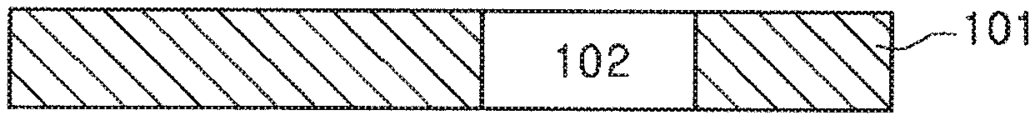
- FIGS. 1 A, 1 B and 2 show the cross-section of a polishing pad according to an
- polishing layer 102 window 103: adhesive layer 104: support layer 201: penetrating hole or first penetrating hole 202: second penetrating hole 203: third penetrating hole
- the polishing pad comprises a polishing layer having to a penetrating hole; and a window inserted in the penetrating hole, wherein the difference in wet hardness between the window and the polishing layer is 0.1 Shore D to 12 Shore D, and the wet hardness is a surface hardness measured upon immersion in water for 30 minutes.
- the polishing pad according to an embodiment comprises a polishing layer ( 101 ) having a penetrating hole ( 201 ) and a window ( 102 ) inserted in the penetrating hole.
- the window may have a wet hardness of 50 Shore D to 75 Shore D in the temperature range of 30° C. to 70° C. Specifically, the window may have a wet hardness of 50 Shore D to 65 Shore D, 52 Shore D to 65 Shore D, 52 Shore D to 63 Shore D, or 60 Shore D to 75 Shore D in the temperature range of 30° C. to 70° C.
- the window may have a wet hardness of 60 Shore D to 75 Shore D at a temperature of 30° C.
- the window may have a wet hardness of 56 Shore D to 68 Shore D at a temperature of 50° C.
- the window may have a wet hardness of 50 Shore D to 66 Shore D at a temperature of 70° C.
- the window may have a wet hardness of 60 Shore D to 63 Shore D at a temperature of 30° C., a wet hardness of 55 Shore D to 58 Shore D at a temperature of 50° C., and a wet hardness of 50 Shore D to 53 Shore D at a temperature of 70° C.
- the window may have a rate of reduction in wet hardness of 20 Shore D/° C. to 25 Shore D/° C. in the temperature range of 30° C. to 70° C.
- the rate of reduction in wet hardness may be calculated by the following Equation 1.
- the window may have a rate of reduction in wet hardness of 21 Shore D/° C. to 23 Shore D/° C. in the temperature range of 30° C. to 70° C.
- Rate of reduction in wet hardness (wet hardness at 30° C. ⁇ wet hardness at 70° C.) ⁇ 100/(70° C. ⁇ 30° C.) [Equation 1]
- the window may be formed from a window composition that comprises a second urethane-based prepolymer and a curing agent.
- the content of the unreacted isocyanate group (NCO) in the second urethane-based prepolymer may be 8.1% by weight to 9.0% by weight.
- the content of the unreacted isocyanate group (NCO) in the second urethane-based prepolymer may be 8.5% by weight to 9.0% by weight.
- a prepolymer generally refers to a polymer having a relatively low molecular weight wherein the degree of polymerization is adjusted to an intermediate level for the sake of convenient molding a product in the process of producing the same.
- a prepolymer may be molded by itself or after a reaction with another polymerizable compound.
- the urethane-based prepolymer may be prepared by reacting an isocyanate compound with a polyol and may comprise an unreacted isocyanate group (NCO).
- the curing agent may be at least one selected from an amine compound and an alcohol compound.
- the curing agent may comprise at least one compound selected from the group consisting of an aromatic amine, an aliphatic amine, an aromatic alcohol, and an aliphatic alcohol.
- the curing agent may be at least one selected from the group consisting of 4,4′-methylenebis(2-chloroaniline) (MOCA), diethyltoluenediamine, diaminodiphenylmethane, diaminodiphenylsulfone, m-xylylenediamine, isophoronediamine, ethylenediamine, diethylenetriamine, triethylenetetramine, polypropylenediamine, polypropylenetriamine, ethylene glycol, diethylene glycol, dipropylene glycol, butanediol, hexanediol, glycerin, trimethylolpropane, and bis(4-amino-3-chlorophenyl)methane.
- MOCA 4,4′-methylenebis(2-chloroaniline)
- diethyltoluenediamine diethyltoluenediamine
- diaminodiphenylmethane diaminodiphenyl
- the window may have the same size as that of the penetrating hole.
- the window may be a non-foam. Since the window has no microbubbles therein, it is possible to reduce the possibility for a polishing liquid to penetrate into the polishing pad, resulting in improvements in the accuracy of optically detecting the termination point and prevention of damage to the light transmission region.
- the window may have a light transmittance of 20% or higher or 30% or higher for light of 400 nm to 700 nm.
- the polishing layer may have a wet hardness of 45 Shore D to 65 Shore D in the temperature range of 30° C. to 70° C. Specifically, the polishing layer may have a wet hardness of 50 Shore D to 65 Shore D or 50 Shore D to 61 Shore D in the temperature range of 30° C. to 70° C.
- the polishing layer may have a wet hardness of 55 Shore D to 65 Shore D at a temperature of 30° C.
- the polishing layer may have a wet hardness of 50 Shore D to 60 Shore D at a temperature of 50° C.
- the polishing layer may have a wet hardness of 45 Shore D to 55 Shore D at a temperature of 70° C.
- the polishing layer may have a wet hardness of 55 Shore D to 61 Shore D at a temperature of 30° C., a wet hardness of 53 Shore D to 56 Shore D at a temperature of 50° C., and a wet hardness of 50 Shore D to 53 Shore D at a temperature of 70° C.
- the polishing layer may have a rate of reduction in wet hardness of 20 Shore D/° C. to 30 Shore D/° C. in the temperature range of 30° C. to 70° C.
- the rate of reduction in wet hardness may be calculated by the following Equation 1.
- the polishing layer may have a rate of reduction in wet hardness of 23 Shore D/° C. to 27 Shore D/° C. in the temperature range of 30° C. to 70° C.
- Rate of reduction in wet hardness (wet hardness at 30° C. ⁇ wet hardness at 70° C.) ⁇ 100/(70° C. ⁇ 30° C.) [Equation 1]
- the polishing layer may be formed from a polishing layer composition that comprises a first urethane-based prepolymer, a curing agent, and a foaming agent.
- the content of the unreacted isocyanate group (NCO) in the first urethane-based prepolymer may be 7.5% by weight to 9.5% by weight.
- the content of the unreacted isocyanate group (NCO) in the first urethane-based prepolymer may be 8.0% by weight to 8.5% by weight.
- the urethane-based prepolymer may be prepared by reacting an isocyanate compound with a polyol and may comprise an unreacted isocyanate group (NCO).
- the difference in the content of the unreacted isocyanate groups (NCO) between the first urethane-based prepolymer and the second urethane-based prepolymer may be 0.4% by weight to 1.0% by weight. Specifically, the difference in the content of the unreacted isocyanate groups (NCO) between the first urethane-based prepolymer and the second urethane-based prepolymer may be 0.5% by weight to 0.8% by weight.
- the curing agent is as described in the above with respect to the window.
- the foaming agent is not particularly limited as long as it is commonly used for forming voids in a polishing pad.
- the foaming agent may be at least one selected from the group consisting of a solid foaming agent having a void, a liquid foaming agent filled with a volatile liquid, and an inert gas.
- the thickness of the polishing layer is not particularly limited. For example, it may be 0.8 mm to 5.0 mm, 1.0 mm to 4.0 mm, or 1.0 mm to 3.0 mm.
- the polishing layer may be formed from a polishing layer composition that comprises a first urethane-based prepolymer, a curing agent, and a foaming agent; and the window may be formed from a window composition that comprises a second urethane-based prepolymer and a curing agent, wherein the difference in the content of the unreacted isocyanate groups (NCO) between the first urethane-based prepolymer and the second urethane-based prepolymer may be 0.4% by weight to 1.0% by weight.
- NCO unreacted isocyanate groups
- the content of the unreacted isocyanate group (NCO) in the first urethane-based prepolymer may be 7.5% by weight to 9.5% by weight; and the content of the unreacted isocyanate group (NCO) in the second urethane-based prepolymer may be 8.1% by weight to 9.0% by weight.
- the difference in wet hardness between the window and the polishing layer may be 0.1 Shore D to 12 Shore D. Specifically, the difference in wet hardness between the window and the polishing layer may be 0.1 Shore D to 10 Shore D. More specifically, the wet hardness of the window may be greater than the wet hardness of the polishing layer by 0.1 Shore D to 10 Shore D, 0.1 Shore D to 8 Shore D, 0.5 Shore D to 8 Shore D, or 1 Shore D to 5 Shore D.
- the difference in wet hardness between the window and the polishing layer is within the above range, it is advantageous to prevent defects on the surface of a wafer during a CMP process, and it is possible to minimize the possibilities that a polishing liquid penetrates into the polishing pad due to the deformation of the window, resulting in an error in the detection of the termination point.
- the polishing layer may have a wet hardness of 45 Shore D to 65 Shore D in the temperature range of 30° C. to 70° C.
- the window may have a wet hardness of 50 Shore D to 75 Shore D in the temperature range of 30° C. to 70° C.
- the difference in the rate of reduction in wet hardness between the window and the polishing layer may be 1 Shore D/° C. to 5 Shore D/° C. in the temperature range of 30° C. to 70° C.
- the rate of reduction in wet hardness may be calculated by the above Equation 1.
- the difference in the rate of reduction in wet hardness between the window and the polishing layer may be 1 Shore D/° C. to 3 Shore D/° C., 2 Shore D/° C. to 4 Shore D/° C., or 3 Shore D/° C. to 5 Shore D/° C.
- the polishing pad may have a deviation in hardness between the window and the polishing layer of 0.1% to 13% in the temperature range of 30° C. to 70° C.
- the deviation in hardness may be calculated by the following Equation 2.
- the polishing pad may have a deviation in hardness between the window and the polishing layer of 0.1% to 10%, 0.5% to 10%, 1% to 8%, or 2% to 7%, in the temperature range of 30° C. to 70° C.
- Deviation in hardness (wet hardness of a window ⁇ wet hardness of a polishing layer) ⁇ 100/(wet hardness of a polishing layer) [Equation 2]
- the deviation in hardness between the window and the polishing layer is within the above range, it is possible to maintain a similar hardness despite a change in temperature during a CMP process, thereby further preventing such defects as scratches on the surface of a wafer during a CMP process.
- the window may have a wear rate that is the same as, or slightly higher than, the wear rate of the polishing layer. In such event, it is possible to prevent the problem that the window portion only is protruded after polishing is carried out for a certain period of time, whereby scratches are generated on the wafer to be polished.
- the wear rate of the polishing layer may be 80% to 100% of the wear rate of the window. More specifically, the wear rate of the polishing layer may be 90% to 100% of the wear rate of the window.
- the wear rate is measured as a percentage of the weight worn by polishing relative to the weight before polishing while the polishing is conducted under the conditions of a load of 1,000 g, an abrasive wheel of H-22, and a rotation of 1,000 revolutions with a wear tester (e.g., Model 174, Taber).
- a wear tester e.g., Model 174, Taber
- Example 1 Production of a Polishing Pad
- the urethane-based prepolymer, the curing agent, the reaction rate controlling agent, and the inert gas were stirred while they were fed to the mixing head at constant rates through the respective feeding lines.
- the molar equivalent ratio of the NCO group in the urethane-based prepolymer to the reactive groups in the curing agent was adjusted to 1:1, and the total feeding amount was maintained at a rate of 10 kg/min.
- the reaction rate controlling agent was fed in an amount of 0.5 part by weight based on 100 parts by weight of the urethane-based prepolymer.
- the argon gas was fed in a volume of 20% based on the total volume of the urethane-based prepolymer.
- the mixed raw materials were injected into a mold (having a width of 1,000 mm, a length of 1,000 mm, and a height of 3 mm) and solidified to obtain a polishing layer in the form of a sheet.
- the surface of the polishing layer was ground to adjust the average thickness to 2 mm.
- a window in the form of a cake was obtained in the same manner as in the above step 1-1, except that PUGL-500D (SKC) having an unreacted NCO content of 8.5% by weight was used as a urethane-based prepolymer, an inert gas was not fed, and the stirred raw materials were injected into a mold (having a width of 1,000 mm, a length of 1,000 mm, and a height of 50 mm).
- PUGL-500D SSC
- the cake was cut and ground to produce twenty windows in the form of a sheet having an average thickness of 1.9 mm.
- the window in the form of a sheet was punched to obtain a window having a width of 20 mm, a length of 60 mm, and a thickness of 1.9 mm.
- a non-woven type support layer (manufacturer: PTS, product name: ND-5400H) having a thickness of 1.1 T was used.
- the polishing layer obtained in the above step 1-1 was punched at a width of 20 mm and a length of 60 mm to form a first penetrating hole, and the support layer obtained in the above step 1-3 was punched at a width of 16 mm and a length of 56 mm to form a second penetrating hole. Then, the polishing layer was thermally bonded to one side of the support layer at 120° C. with a hot-melt film (manufacturer SKC, product name: TF-00). A double-sided adhesive tape (manufacturer: 3M, product name: 442JS) was attached to the other side of the support layer.
- the double-sided adhesive tape corresponding to the second penetrating hole was cut and removed to form a third penetrating hole.
- the window obtained in the above step 1-2 was inserted into the first penetrating hole and adhered to the double-sided adhesive tape to prepare a polishing pad (see FIG. 2 ).
- a polishing pad was prepared in the same manner as in Example 1, except that PUGL-550D (SKC) having an unreacted NCO content of 9.1% by weight was used as a urethane-based prepolymer in the production of a window.
- SSC PUGL-550D
- a polishing pad was prepared in the same manner as in Example 1, except that PUGL-450D (SKC) having an unreacted NCO content of 8.0% by weight was used as a urethane-based prepolymer in the production of a window.
- SSC PUGL-450D
- polishing layers and the windows prepared in Examples 1 and 2 and Comparative Example 1 were each cut into a size of 2 cm ⁇ 2 cm (thickness: 2 mm), immersed in water at 30° C., 50° C., or 70° C. for 30 minutes, and the hardness was measured using a hardness meter (D-type hardness meter). The measurement results are shown in Table 1 below.
- the polishing pads of Examples 1 and 2 each had a difference in wet hardness of less than 12 Shore D between the polishing layer and the window. Particularly, the polishing pad of Example 1 had a remarkably low difference in wet hardness of 3 Shore D or less between the polishing layer and the window. In contrast, the polishing pad of Comparative Example 1 had a difference in wet hardness of 16.4 Shore D to the maximum between the polishing layer and the window. If the polishing pad of Comparative Example 1 were used in a CMP process, there would be a problem that such defects as scratches are generated on the surface of a wafer.
- polishing pad of Example 1 had a remarkable low deviation in hardness of less than 6% between the polishing layer and the window, whereas the polishing pad of Comparative Example 1 had a very high deviation in hardness of 30%/o or more to the maximum between the polishing layer and the window.
- the rate of reduction in wet hardness of the polishing layer was similar to that of the window.
- the polishing pad of Comparative Example 1 had a difference in the rate of reduction in wet hardness of 20 Shore D/° C. or higher between the polishing layer and the window.
Landscapes
- Engineering & Computer Science (AREA)
- Mechanical Engineering (AREA)
- Mechanical Treatment Of Semiconductor (AREA)
- Finish Polishing, Edge Sharpening, And Grinding By Specific Grinding Devices (AREA)
- Polyurethanes Or Polyureas (AREA)
- Physics & Mathematics (AREA)
- Condensed Matter Physics & Semiconductors (AREA)
- General Physics & Mathematics (AREA)
- Manufacturing & Machinery (AREA)
- Computer Hardware Design (AREA)
- Microelectronics & Electronic Packaging (AREA)
- Power Engineering (AREA)
Abstract
Description
| <Reference Numerals of the Drawings> |
| 101: polishing layer | 102: window |
| 103: adhesive layer | 104: support layer |
| 201: penetrating hole or first penetrating hole | |
| 202: second penetrating hole | 203: third penetrating hole |
Rate of reduction in wet hardness=(wet hardness at 30° C.−wet hardness at 70° C.)×100/(70° C.−30° C.) [Equation 1]
Rate of reduction in wet hardness=(wet hardness at 30° C.−wet hardness at 70° C.)×100/(70° C.−30° C.) [Equation 1]
Deviation in hardness=(wet hardness of a window−wet hardness of a polishing layer)×100/(wet hardness of a polishing layer) [Equation 2]
Rate of reduction in wet hardness=(wet hardness at 30° C.−wet hardness at 70° C.)×100/(70° C.−30° C.) [Equation 1]
Deviation in hardness=(wet hardness of a window−wet hardness of a polishing layer)×100/(wet hardness of a polishing layer) [Equation 2]
| TABLE 1 | ||
| Polishing | Window | |
| layer | Ex. 1 | Ex. 2 | C. Ex. 1 | |
| Wet hardness | 30° C. | 60.5 | 62.2 | 70.8 | 68.8 |
| (shore D) | 50° C. | 55.7 | 57.3 | 65.9 | 67.8 |
| 70° C. | 50.2 | 53.1 | 61.7 | 66.6 | |
| Difference in wet | 30° C. | — | 1.7 | 10.3 | 8.8 |
| hardness (shore D) | 50° C. | — | 1.6 | 10.2 | 12.1 |
| 70° C. | — | 2.9 | 11.5 | 16.4 | |
| Deviation in hardness | 30° C. | — | 2.81 | 17.02 | 14.5 |
| (%) | 50° C. | — | 2.87 | 18.31 | 21.7 |
| 70° C. | — | 5.78 | 22.91 | 32.67 |
| Rate of reduction in wet hardness | 25.75 | 22.75 | 22.75 | 5.50 |
| (shore D/° C.) | ||||
Claims (7)
Rate of reduction in wet hardness=(wet hardness at 30° C.−wet hardness at 70° C.)×100/(70° C.−30° C.). [Equation 1]
Rate of reduction in wet hardness=(wet hardness at 30° C.−wet hardness at 70° C.)×100/(70° C.−30° C.). [Equation 1]
Deviation in hardness=(wet hardness of a window−wet hardness of a polishing layer)×100/(wet hardness of a polishing layer). [Equation 2]
Applications Claiming Priority (3)
| Application Number | Priority Date | Filing Date | Title |
|---|---|---|---|
| KR1020170087720A KR101945878B1 (en) | 2017-07-11 | 2017-07-11 | Polishing pad comprising window having similar hardness with polishing layer |
| KR10-2017-0087720 | 2017-07-11 | ||
| PCT/KR2018/007805 WO2019013523A1 (en) | 2017-07-11 | 2018-07-10 | Polishing pad comprising window similar in hardness to polishing layer |
Publications (2)
| Publication Number | Publication Date |
|---|---|
| US20200164483A1 US20200164483A1 (en) | 2020-05-28 |
| US11964360B2 true US11964360B2 (en) | 2024-04-23 |
Family
ID=65002087
Family Applications (1)
| Application Number | Title | Priority Date | Filing Date |
|---|---|---|---|
| US16/619,378 Active 2041-08-21 US11964360B2 (en) | 2017-07-11 | 2018-07-10 | Polishing pad comprising window similar in hardness to polishing layer |
Country Status (6)
| Country | Link |
|---|---|
| US (1) | US11964360B2 (en) |
| JP (1) | JP6912599B2 (en) |
| KR (1) | KR101945878B1 (en) |
| CN (1) | CN110785259B (en) |
| TW (1) | TWI691589B (en) |
| WO (1) | WO2019013523A1 (en) |
Families Citing this family (10)
| Publication number | Priority date | Publication date | Assignee | Title |
|---|---|---|---|---|
| KR102237357B1 (en) * | 2019-06-17 | 2021-04-07 | 에스케이씨솔믹스 주식회사 | Composition for polishing pad, polishing pad and preparation method of semiconductor device |
| JP7812706B2 (en) * | 2021-03-30 | 2026-02-10 | 富士紡ホールディングス株式会社 | Polishing pad and method for manufacturing polished workpiece |
| WO2022210264A1 (en) * | 2021-03-30 | 2022-10-06 | 富士紡ホールディングス株式会社 | Polishing pad and method for manufacturing polished workpiece |
| JP7650698B2 (en) * | 2021-03-30 | 2025-03-25 | 富士紡ホールディングス株式会社 | Method for manufacturing polishing pad and polished product |
| CN115555986B (en) * | 2021-07-02 | 2025-12-19 | 恩普士有限公司 | Polishing pad and method for manufacturing semiconductor device using the same |
| KR102623920B1 (en) * | 2021-07-27 | 2024-01-10 | 에스케이엔펄스 주식회사 | Polishing pad and preparing method of semiconductor device using the same |
| KR102624629B1 (en) * | 2021-11-19 | 2024-01-15 | 에스케이하이닉스 주식회사 | Window insert type polishing pad and method for manufacturing the same |
| KR102641899B1 (en) * | 2021-11-25 | 2024-02-27 | 에스케이엔펄스 주식회사 | Polishing pad and preparing method of semiconductor device using the same |
| JP7804502B2 (en) * | 2022-03-24 | 2026-01-22 | 富士紡ホールディングス株式会社 | Polishing pad and method for manufacturing polished workpiece |
| CN120572457B (en) * | 2025-08-05 | 2025-12-02 | 万华化学集团电子材料有限公司 | Endpoint detection window and preparation method and application thereof |
Citations (13)
| Publication number | Priority date | Publication date | Assignee | Title |
|---|---|---|---|---|
| JP2001015861A (en) | 1999-07-01 | 2001-01-19 | Fuji Photo Film Co Ltd | Semiconductor laser device |
| JP2003507199A (en) | 1999-08-17 | 2003-02-25 | ロデール ホールディングス インコーポレイテッド | Molded polishing pad with integrated window |
| KR20030047893A (en) | 2000-06-05 | 2003-06-18 | 스피드팸-아이펙 코퍼레이션 | Polishing pad window for a chemical-mechanical polishing tool |
| US20040033758A1 (en) | 2001-12-28 | 2004-02-19 | Wiswesser Andreas Norbert | Polishing pad with window |
| JP2006527476A (en) | 2003-04-17 | 2006-11-30 | ピーピージー インダストリーズ オハイオ, インコーポレイテッド | Polishing pad with window |
| KR100707959B1 (en) | 1999-09-29 | 2007-04-16 | 롬 앤드 하스 일렉트로닉 머티리얼스 씨엠피 홀딩스 인코포레이티드 | Polishing pad |
| JP2009066675A (en) | 2007-09-11 | 2009-04-02 | Fujibo Holdings Inc | Polishing pad and polishing pad manufacturing method |
| JP2011031392A (en) | 2003-06-17 | 2011-02-17 | Cabot Microelectronics Corp | Ultrasonic welding method for manufacturing polishing pad comprising optically transmissive region |
| JP2011051045A (en) | 2009-08-31 | 2011-03-17 | Fujibo Holdings Inc | Method of manufacturing polishing pad |
| KR20140144075A (en) | 2013-06-10 | 2014-12-18 | 삼성전자주식회사 | Polishing pad compound |
| JP2015047691A (en) | 2013-08-30 | 2015-03-16 | ローム アンド ハース エレクトロニック マテリアルズ シーエムピー ホウルディングス インコーポレイテッド | Chemical mechanical polishing pad |
| JP2015211224A (en) | 2014-04-29 | 2015-11-24 | ローム アンド ハース エレクトロニック マテリアルズ シーエムピー ホウルディングス インコーポレイテッド | Chemical mechanical polishing pad with end point detection window |
| US9259820B2 (en) * | 2014-03-28 | 2016-02-16 | Rohm And Haas Electronic Materials Cmp Holdings, Inc. | Chemical mechanical polishing pad with polishing layer and window |
Family Cites Families (4)
| Publication number | Priority date | Publication date | Assignee | Title |
|---|---|---|---|---|
| JP3867844B2 (en) * | 1999-08-27 | 2007-01-17 | 旭化成エレクトロニクス株式会社 | Polishing pad and polishing apparatus |
| CN1285457C (en) * | 2002-12-06 | 2006-11-22 | 智胜科技股份有限公司 | Manufacturing method of polishing pad with detection window |
| JP5426469B2 (en) * | 2010-05-10 | 2014-02-26 | 東洋ゴム工業株式会社 | Polishing pad and glass substrate manufacturing method |
| US9064806B1 (en) | 2014-03-28 | 2015-06-23 | Rohm and Haas Electronics Materials CMP Holdings, Inc. | Soft and conditionable chemical mechanical polishing pad with window |
-
2017
- 2017-07-11 KR KR1020170087720A patent/KR101945878B1/en active Active
-
2018
- 2018-07-10 WO PCT/KR2018/007805 patent/WO2019013523A1/en not_active Ceased
- 2018-07-10 TW TW107123856A patent/TWI691589B/en active
- 2018-07-10 US US16/619,378 patent/US11964360B2/en active Active
- 2018-07-10 CN CN201880042418.5A patent/CN110785259B/en active Active
- 2018-07-10 JP JP2019558518A patent/JP6912599B2/en active Active
Patent Citations (13)
| Publication number | Priority date | Publication date | Assignee | Title |
|---|---|---|---|---|
| JP2001015861A (en) | 1999-07-01 | 2001-01-19 | Fuji Photo Film Co Ltd | Semiconductor laser device |
| JP2003507199A (en) | 1999-08-17 | 2003-02-25 | ロデール ホールディングス インコーポレイテッド | Molded polishing pad with integrated window |
| KR100707959B1 (en) | 1999-09-29 | 2007-04-16 | 롬 앤드 하스 일렉트로닉 머티리얼스 씨엠피 홀딩스 인코포레이티드 | Polishing pad |
| KR20030047893A (en) | 2000-06-05 | 2003-06-18 | 스피드팸-아이펙 코퍼레이션 | Polishing pad window for a chemical-mechanical polishing tool |
| US20040033758A1 (en) | 2001-12-28 | 2004-02-19 | Wiswesser Andreas Norbert | Polishing pad with window |
| JP2006527476A (en) | 2003-04-17 | 2006-11-30 | ピーピージー インダストリーズ オハイオ, インコーポレイテッド | Polishing pad with window |
| JP2011031392A (en) | 2003-06-17 | 2011-02-17 | Cabot Microelectronics Corp | Ultrasonic welding method for manufacturing polishing pad comprising optically transmissive region |
| JP2009066675A (en) | 2007-09-11 | 2009-04-02 | Fujibo Holdings Inc | Polishing pad and polishing pad manufacturing method |
| JP2011051045A (en) | 2009-08-31 | 2011-03-17 | Fujibo Holdings Inc | Method of manufacturing polishing pad |
| KR20140144075A (en) | 2013-06-10 | 2014-12-18 | 삼성전자주식회사 | Polishing pad compound |
| JP2015047691A (en) | 2013-08-30 | 2015-03-16 | ローム アンド ハース エレクトロニック マテリアルズ シーエムピー ホウルディングス インコーポレイテッド | Chemical mechanical polishing pad |
| US9259820B2 (en) * | 2014-03-28 | 2016-02-16 | Rohm And Haas Electronic Materials Cmp Holdings, Inc. | Chemical mechanical polishing pad with polishing layer and window |
| JP2015211224A (en) | 2014-04-29 | 2015-11-24 | ローム アンド ハース エレクトロニック マテリアルズ シーエムピー ホウルディングス インコーポレイテッド | Chemical mechanical polishing pad with end point detection window |
Also Published As
| Publication number | Publication date |
|---|---|
| KR101945878B1 (en) | 2019-02-11 |
| US20200164483A1 (en) | 2020-05-28 |
| TWI691589B (en) | 2020-04-21 |
| CN110785259A (en) | 2020-02-11 |
| CN110785259B (en) | 2022-03-04 |
| KR20190006699A (en) | 2019-01-21 |
| JP6912599B2 (en) | 2021-08-04 |
| TW201908456A (en) | 2019-03-01 |
| WO2019013523A1 (en) | 2019-01-17 |
| JP2020519458A (en) | 2020-07-02 |
Similar Documents
| Publication | Publication Date | Title |
|---|---|---|
| US11964360B2 (en) | Polishing pad comprising window similar in hardness to polishing layer | |
| US11207757B2 (en) | Composition for polishing pad, polishing pad and preparation method of semiconductor device | |
| US11548970B2 (en) | Composition for a polishing pad, polishing pad, and process for preparing the same | |
| CN103608903A (en) | Polishing pad and manufacturing method therefor | |
| US11279825B2 (en) | Composition for polishing pad, polishing pad and preparation method thereof | |
| KR101945874B1 (en) | Surface treated window for polishing pad and polishing pad comprising the same | |
| US20210129285A1 (en) | Polishing pad, process for preparing the same, and process for preparing a semiconductor device using the same | |
| KR102197481B1 (en) | Polishing pad and preparation method thereof | |
| JP7527317B2 (en) | Polishing pad with controlled crosslinking degree and manufacturing method thereof | |
| US11571783B2 (en) | Polishing pad having excellent airtightness | |
| KR102293781B1 (en) | Polishing pad, preparation method thereof, and preparation method of semiconductor device using same | |
| KR102362791B1 (en) | Polishing pad and preparation method of semiconductor device using same | |
| KR102367144B1 (en) | Polishing pad with improved crosslinking density and preparation method thereof | |
| KR20200079840A (en) | Composition for polishing pad, polishing pad and preparation method thereof | |
| KR102237362B1 (en) | Composition for polishing pad, polishing pad and preparation method of semiconductor device | |
| KR102237367B1 (en) | Composition for polishing pad, polishing pad and preparation method of semiconductor device | |
| KR102298114B1 (en) | Polishing pad, preparation method thereof, and preparation method of semiconductor device using same | |
| CN113410163A (en) | Polishing sheet and method for manufacturing semiconductor device using the same | |
| KR102237351B1 (en) | Composition for polishing pad, polishing pad and preparation method of semiconductor device | |
| KR102237357B1 (en) | Composition for polishing pad, polishing pad and preparation method of semiconductor device | |
| KR20200079865A (en) | Composition for polishing pad, polishing pad and preparation method thereof | |
| KR20200079847A (en) | Composition for polishing pad, polishing pad and preparation method thereof |
Legal Events
| Date | Code | Title | Description |
|---|---|---|---|
| AS | Assignment |
Owner name: SKC CO., LTD., KOREA, REPUBLIC OF Free format text: ASSIGNMENT OF ASSIGNORS INTEREST;ASSIGNORS:YUN, SUNGHOON;RYOU, JOONSUNG;SEO, JANG WON;AND OTHERS;REEL/FRAME:051179/0338 Effective date: 20190905 |
|
| FEPP | Fee payment procedure |
Free format text: ENTITY STATUS SET TO UNDISCOUNTED (ORIGINAL EVENT CODE: BIG.); ENTITY STATUS OF PATENT OWNER: LARGE ENTITY |
|
| STPP | Information on status: patent application and granting procedure in general |
Free format text: APPLICATION DISPATCHED FROM PREEXAM, NOT YET DOCKETED |
|
| AS | Assignment |
Owner name: SKC SOLMICS CO., LTD., KOREA, REPUBLIC OF Free format text: ASSIGNMENT OF ASSIGNORS INTEREST;ASSIGNOR:SKC CO., LTD.;REEL/FRAME:055685/0677 Effective date: 20210302 |
|
| STPP | Information on status: patent application and granting procedure in general |
Free format text: DOCKETED NEW CASE - READY FOR EXAMINATION |
|
| AS | Assignment |
Owner name: SK ENPULSE CO., LTD., KOREA, REPUBLIC OF Free format text: CHANGE OF NAME;ASSIGNOR:SKC SOLMICS CO., LTD.;REEL/FRAME:062717/0084 Effective date: 20230101 |
|
| STPP | Information on status: patent application and granting procedure in general |
Free format text: NON FINAL ACTION MAILED |
|
| STPP | Information on status: patent application and granting procedure in general |
Free format text: RESPONSE TO NON-FINAL OFFICE ACTION ENTERED AND FORWARDED TO EXAMINER |
|
| STPP | Information on status: patent application and granting procedure in general |
Free format text: NOTICE OF ALLOWANCE MAILED -- APPLICATION RECEIVED IN OFFICE OF PUBLICATIONS |
|
| ZAAB | Notice of allowance mailed |
Free format text: ORIGINAL CODE: MN/=. |
|
| STPP | Information on status: patent application and granting procedure in general |
Free format text: PUBLICATIONS -- ISSUE FEE PAYMENT VERIFIED |
|
| STCF | Information on status: patent grant |
Free format text: PATENTED CASE |
|
| AS | Assignment |
Owner name: ENPULSE CO., LTD., KOREA, REPUBLIC OF Free format text: ASSIGNMENT OF ASSIGNORS INTEREST;ASSIGNOR:SK ENPULSE CO., LTD.;REEL/FRAME:071277/0667 Effective date: 20250425 Owner name: ENPULSE CO., LTD., KOREA, REPUBLIC OF Free format text: ASSIGNMENT OF ASSIGNOR'S INTEREST;ASSIGNOR:SK ENPULSE CO., LTD.;REEL/FRAME:071277/0667 Effective date: 20250425 |