US11922888B2 - Display device, data driving circuit and display driving method - Google Patents
Display device, data driving circuit and display driving method Download PDFInfo
- Publication number
- US11922888B2 US11922888B2 US17/837,194 US202217837194A US11922888B2 US 11922888 B2 US11922888 B2 US 11922888B2 US 202217837194 A US202217837194 A US 202217837194A US 11922888 B2 US11922888 B2 US 11922888B2
- Authority
- US
- United States
- Prior art keywords
- data
- gamma
- driving
- driving power
- circuit
- Prior art date
- Legal status (The legal status is an assumption and is not a legal conclusion. Google has not performed a legal analysis and makes no representation as to the accuracy of the status listed.)
- Active
Links
Images


Classifications
-
- G—PHYSICS
- G09—EDUCATION; CRYPTOGRAPHY; DISPLAY; ADVERTISING; SEALS
- G09G—ARRANGEMENTS OR CIRCUITS FOR CONTROL OF INDICATING DEVICES USING STATIC MEANS TO PRESENT VARIABLE INFORMATION
- G09G3/00—Control arrangements or circuits, of interest only in connection with visual indicators other than cathode-ray tubes
- G09G3/20—Control arrangements or circuits, of interest only in connection with visual indicators other than cathode-ray tubes for presentation of an assembly of a number of characters, e.g. a page, by composing the assembly by combination of individual elements arranged in a matrix no fixed position being assigned to or needed to be assigned to the individual characters or partial characters
- G09G3/22—Control arrangements or circuits, of interest only in connection with visual indicators other than cathode-ray tubes for presentation of an assembly of a number of characters, e.g. a page, by composing the assembly by combination of individual elements arranged in a matrix no fixed position being assigned to or needed to be assigned to the individual characters or partial characters using controlled light sources
- G09G3/30—Control arrangements or circuits, of interest only in connection with visual indicators other than cathode-ray tubes for presentation of an assembly of a number of characters, e.g. a page, by composing the assembly by combination of individual elements arranged in a matrix no fixed position being assigned to or needed to be assigned to the individual characters or partial characters using controlled light sources using electroluminescent panels
- G09G3/32—Control arrangements or circuits, of interest only in connection with visual indicators other than cathode-ray tubes for presentation of an assembly of a number of characters, e.g. a page, by composing the assembly by combination of individual elements arranged in a matrix no fixed position being assigned to or needed to be assigned to the individual characters or partial characters using controlled light sources using electroluminescent panels semiconductive, e.g. using light-emitting diodes [LED]
- G09G3/3208—Control arrangements or circuits, of interest only in connection with visual indicators other than cathode-ray tubes for presentation of an assembly of a number of characters, e.g. a page, by composing the assembly by combination of individual elements arranged in a matrix no fixed position being assigned to or needed to be assigned to the individual characters or partial characters using controlled light sources using electroluminescent panels semiconductive, e.g. using light-emitting diodes [LED] organic, e.g. using organic light-emitting diodes [OLED]
- G09G3/3275—Details of drivers for data electrodes
-
- G—PHYSICS
- G09—EDUCATION; CRYPTOGRAPHY; DISPLAY; ADVERTISING; SEALS
- G09G—ARRANGEMENTS OR CIRCUITS FOR CONTROL OF INDICATING DEVICES USING STATIC MEANS TO PRESENT VARIABLE INFORMATION
- G09G3/00—Control arrangements or circuits, of interest only in connection with visual indicators other than cathode-ray tubes
- G09G3/20—Control arrangements or circuits, of interest only in connection with visual indicators other than cathode-ray tubes for presentation of an assembly of a number of characters, e.g. a page, by composing the assembly by combination of individual elements arranged in a matrix no fixed position being assigned to or needed to be assigned to the individual characters or partial characters
- G09G3/2007—Display of intermediate tones
- G09G3/2074—Display of intermediate tones using sub-pixels
-
- G—PHYSICS
- G09—EDUCATION; CRYPTOGRAPHY; DISPLAY; ADVERTISING; SEALS
- G09G—ARRANGEMENTS OR CIRCUITS FOR CONTROL OF INDICATING DEVICES USING STATIC MEANS TO PRESENT VARIABLE INFORMATION
- G09G3/00—Control arrangements or circuits, of interest only in connection with visual indicators other than cathode-ray tubes
- G09G3/20—Control arrangements or circuits, of interest only in connection with visual indicators other than cathode-ray tubes for presentation of an assembly of a number of characters, e.g. a page, by composing the assembly by combination of individual elements arranged in a matrix no fixed position being assigned to or needed to be assigned to the individual characters or partial characters
- G09G3/22—Control arrangements or circuits, of interest only in connection with visual indicators other than cathode-ray tubes for presentation of an assembly of a number of characters, e.g. a page, by composing the assembly by combination of individual elements arranged in a matrix no fixed position being assigned to or needed to be assigned to the individual characters or partial characters using controlled light sources
- G09G3/30—Control arrangements or circuits, of interest only in connection with visual indicators other than cathode-ray tubes for presentation of an assembly of a number of characters, e.g. a page, by composing the assembly by combination of individual elements arranged in a matrix no fixed position being assigned to or needed to be assigned to the individual characters or partial characters using controlled light sources using electroluminescent panels
- G09G3/32—Control arrangements or circuits, of interest only in connection with visual indicators other than cathode-ray tubes for presentation of an assembly of a number of characters, e.g. a page, by composing the assembly by combination of individual elements arranged in a matrix no fixed position being assigned to or needed to be assigned to the individual characters or partial characters using controlled light sources using electroluminescent panels semiconductive, e.g. using light-emitting diodes [LED]
- G09G3/3208—Control arrangements or circuits, of interest only in connection with visual indicators other than cathode-ray tubes for presentation of an assembly of a number of characters, e.g. a page, by composing the assembly by combination of individual elements arranged in a matrix no fixed position being assigned to or needed to be assigned to the individual characters or partial characters using controlled light sources using electroluminescent panels semiconductive, e.g. using light-emitting diodes [LED] organic, e.g. using organic light-emitting diodes [OLED]
- G09G3/3225—Control arrangements or circuits, of interest only in connection with visual indicators other than cathode-ray tubes for presentation of an assembly of a number of characters, e.g. a page, by composing the assembly by combination of individual elements arranged in a matrix no fixed position being assigned to or needed to be assigned to the individual characters or partial characters using controlled light sources using electroluminescent panels semiconductive, e.g. using light-emitting diodes [LED] organic, e.g. using organic light-emitting diodes [OLED] using an active matrix
- G09G3/3233—Control arrangements or circuits, of interest only in connection with visual indicators other than cathode-ray tubes for presentation of an assembly of a number of characters, e.g. a page, by composing the assembly by combination of individual elements arranged in a matrix no fixed position being assigned to or needed to be assigned to the individual characters or partial characters using controlled light sources using electroluminescent panels semiconductive, e.g. using light-emitting diodes [LED] organic, e.g. using organic light-emitting diodes [OLED] using an active matrix with pixel circuitry controlling the current through the light-emitting element
-
- G—PHYSICS
- G09—EDUCATION; CRYPTOGRAPHY; DISPLAY; ADVERTISING; SEALS
- G09G—ARRANGEMENTS OR CIRCUITS FOR CONTROL OF INDICATING DEVICES USING STATIC MEANS TO PRESENT VARIABLE INFORMATION
- G09G3/00—Control arrangements or circuits, of interest only in connection with visual indicators other than cathode-ray tubes
- G09G3/20—Control arrangements or circuits, of interest only in connection with visual indicators other than cathode-ray tubes for presentation of an assembly of a number of characters, e.g. a page, by composing the assembly by combination of individual elements arranged in a matrix no fixed position being assigned to or needed to be assigned to the individual characters or partial characters
- G09G3/22—Control arrangements or circuits, of interest only in connection with visual indicators other than cathode-ray tubes for presentation of an assembly of a number of characters, e.g. a page, by composing the assembly by combination of individual elements arranged in a matrix no fixed position being assigned to or needed to be assigned to the individual characters or partial characters using controlled light sources
- G09G3/30—Control arrangements or circuits, of interest only in connection with visual indicators other than cathode-ray tubes for presentation of an assembly of a number of characters, e.g. a page, by composing the assembly by combination of individual elements arranged in a matrix no fixed position being assigned to or needed to be assigned to the individual characters or partial characters using controlled light sources using electroluminescent panels
- G09G3/32—Control arrangements or circuits, of interest only in connection with visual indicators other than cathode-ray tubes for presentation of an assembly of a number of characters, e.g. a page, by composing the assembly by combination of individual elements arranged in a matrix no fixed position being assigned to or needed to be assigned to the individual characters or partial characters using controlled light sources using electroluminescent panels semiconductive, e.g. using light-emitting diodes [LED]
- G09G3/3208—Control arrangements or circuits, of interest only in connection with visual indicators other than cathode-ray tubes for presentation of an assembly of a number of characters, e.g. a page, by composing the assembly by combination of individual elements arranged in a matrix no fixed position being assigned to or needed to be assigned to the individual characters or partial characters using controlled light sources using electroluminescent panels semiconductive, e.g. using light-emitting diodes [LED] organic, e.g. using organic light-emitting diodes [OLED]
- G09G3/3225—Control arrangements or circuits, of interest only in connection with visual indicators other than cathode-ray tubes for presentation of an assembly of a number of characters, e.g. a page, by composing the assembly by combination of individual elements arranged in a matrix no fixed position being assigned to or needed to be assigned to the individual characters or partial characters using controlled light sources using electroluminescent panels semiconductive, e.g. using light-emitting diodes [LED] organic, e.g. using organic light-emitting diodes [OLED] using an active matrix
- G09G3/3258—Control arrangements or circuits, of interest only in connection with visual indicators other than cathode-ray tubes for presentation of an assembly of a number of characters, e.g. a page, by composing the assembly by combination of individual elements arranged in a matrix no fixed position being assigned to or needed to be assigned to the individual characters or partial characters using controlled light sources using electroluminescent panels semiconductive, e.g. using light-emitting diodes [LED] organic, e.g. using organic light-emitting diodes [OLED] using an active matrix with pixel circuitry controlling the voltage across the light-emitting element
-
- G—PHYSICS
- G09—EDUCATION; CRYPTOGRAPHY; DISPLAY; ADVERTISING; SEALS
- G09G—ARRANGEMENTS OR CIRCUITS FOR CONTROL OF INDICATING DEVICES USING STATIC MEANS TO PRESENT VARIABLE INFORMATION
- G09G3/00—Control arrangements or circuits, of interest only in connection with visual indicators other than cathode-ray tubes
- G09G3/20—Control arrangements or circuits, of interest only in connection with visual indicators other than cathode-ray tubes for presentation of an assembly of a number of characters, e.g. a page, by composing the assembly by combination of individual elements arranged in a matrix no fixed position being assigned to or needed to be assigned to the individual characters or partial characters
- G09G3/22—Control arrangements or circuits, of interest only in connection with visual indicators other than cathode-ray tubes for presentation of an assembly of a number of characters, e.g. a page, by composing the assembly by combination of individual elements arranged in a matrix no fixed position being assigned to or needed to be assigned to the individual characters or partial characters using controlled light sources
- G09G3/30—Control arrangements or circuits, of interest only in connection with visual indicators other than cathode-ray tubes for presentation of an assembly of a number of characters, e.g. a page, by composing the assembly by combination of individual elements arranged in a matrix no fixed position being assigned to or needed to be assigned to the individual characters or partial characters using controlled light sources using electroluminescent panels
- G09G3/32—Control arrangements or circuits, of interest only in connection with visual indicators other than cathode-ray tubes for presentation of an assembly of a number of characters, e.g. a page, by composing the assembly by combination of individual elements arranged in a matrix no fixed position being assigned to or needed to be assigned to the individual characters or partial characters using controlled light sources using electroluminescent panels semiconductive, e.g. using light-emitting diodes [LED]
- G09G3/3208—Control arrangements or circuits, of interest only in connection with visual indicators other than cathode-ray tubes for presentation of an assembly of a number of characters, e.g. a page, by composing the assembly by combination of individual elements arranged in a matrix no fixed position being assigned to or needed to be assigned to the individual characters or partial characters using controlled light sources using electroluminescent panels semiconductive, e.g. using light-emitting diodes [LED] organic, e.g. using organic light-emitting diodes [OLED]
- G09G3/3266—Details of drivers for scan electrodes
-
- G—PHYSICS
- G09—EDUCATION; CRYPTOGRAPHY; DISPLAY; ADVERTISING; SEALS
- G09G—ARRANGEMENTS OR CIRCUITS FOR CONTROL OF INDICATING DEVICES USING STATIC MEANS TO PRESENT VARIABLE INFORMATION
- G09G3/00—Control arrangements or circuits, of interest only in connection with visual indicators other than cathode-ray tubes
- G09G3/20—Control arrangements or circuits, of interest only in connection with visual indicators other than cathode-ray tubes for presentation of an assembly of a number of characters, e.g. a page, by composing the assembly by combination of individual elements arranged in a matrix no fixed position being assigned to or needed to be assigned to the individual characters or partial characters
- G09G3/22—Control arrangements or circuits, of interest only in connection with visual indicators other than cathode-ray tubes for presentation of an assembly of a number of characters, e.g. a page, by composing the assembly by combination of individual elements arranged in a matrix no fixed position being assigned to or needed to be assigned to the individual characters or partial characters using controlled light sources
- G09G3/30—Control arrangements or circuits, of interest only in connection with visual indicators other than cathode-ray tubes for presentation of an assembly of a number of characters, e.g. a page, by composing the assembly by combination of individual elements arranged in a matrix no fixed position being assigned to or needed to be assigned to the individual characters or partial characters using controlled light sources using electroluminescent panels
- G09G3/32—Control arrangements or circuits, of interest only in connection with visual indicators other than cathode-ray tubes for presentation of an assembly of a number of characters, e.g. a page, by composing the assembly by combination of individual elements arranged in a matrix no fixed position being assigned to or needed to be assigned to the individual characters or partial characters using controlled light sources using electroluminescent panels semiconductive, e.g. using light-emitting diodes [LED]
- G09G3/3208—Control arrangements or circuits, of interest only in connection with visual indicators other than cathode-ray tubes for presentation of an assembly of a number of characters, e.g. a page, by composing the assembly by combination of individual elements arranged in a matrix no fixed position being assigned to or needed to be assigned to the individual characters or partial characters using controlled light sources using electroluminescent panels semiconductive, e.g. using light-emitting diodes [LED] organic, e.g. using organic light-emitting diodes [OLED]
- G09G3/3275—Details of drivers for data electrodes
- G09G3/3291—Details of drivers for data electrodes in which the data driver supplies a variable data voltage for setting the current through, or the voltage across, the light-emitting elements
-
- G—PHYSICS
- G09—EDUCATION; CRYPTOGRAPHY; DISPLAY; ADVERTISING; SEALS
- G09G—ARRANGEMENTS OR CIRCUITS FOR CONTROL OF INDICATING DEVICES USING STATIC MEANS TO PRESENT VARIABLE INFORMATION
- G09G2300/00—Aspects of the constitution of display devices
- G09G2300/04—Structural and physical details of display devices
- G09G2300/0439—Pixel structures
- G09G2300/0452—Details of colour pixel setup, e.g. pixel composed of a red, a blue and two green components
-
- G—PHYSICS
- G09—EDUCATION; CRYPTOGRAPHY; DISPLAY; ADVERTISING; SEALS
- G09G—ARRANGEMENTS OR CIRCUITS FOR CONTROL OF INDICATING DEVICES USING STATIC MEANS TO PRESENT VARIABLE INFORMATION
- G09G2300/00—Aspects of the constitution of display devices
- G09G2300/08—Active matrix structure, i.e. with use of active elements, inclusive of non-linear two terminal elements, in the pixels together with light emitting or modulating elements
- G09G2300/0809—Several active elements per pixel in active matrix panels
- G09G2300/0819—Several active elements per pixel in active matrix panels used for counteracting undesired variations, e.g. feedback or autozeroing
-
- G—PHYSICS
- G09—EDUCATION; CRYPTOGRAPHY; DISPLAY; ADVERTISING; SEALS
- G09G—ARRANGEMENTS OR CIRCUITS FOR CONTROL OF INDICATING DEVICES USING STATIC MEANS TO PRESENT VARIABLE INFORMATION
- G09G2300/00—Aspects of the constitution of display devices
- G09G2300/08—Active matrix structure, i.e. with use of active elements, inclusive of non-linear two terminal elements, in the pixels together with light emitting or modulating elements
- G09G2300/0809—Several active elements per pixel in active matrix panels
- G09G2300/0842—Several active elements per pixel in active matrix panels forming a memory circuit, e.g. a dynamic memory with one capacitor
-
- G—PHYSICS
- G09—EDUCATION; CRYPTOGRAPHY; DISPLAY; ADVERTISING; SEALS
- G09G—ARRANGEMENTS OR CIRCUITS FOR CONTROL OF INDICATING DEVICES USING STATIC MEANS TO PRESENT VARIABLE INFORMATION
- G09G2310/00—Command of the display device
- G09G2310/02—Addressing, scanning or driving the display screen or processing steps related thereto
- G09G2310/0264—Details of driving circuits
- G09G2310/027—Details of drivers for data electrodes, the drivers handling digital grey scale data, e.g. use of D/A converters
-
- G—PHYSICS
- G09—EDUCATION; CRYPTOGRAPHY; DISPLAY; ADVERTISING; SEALS
- G09G—ARRANGEMENTS OR CIRCUITS FOR CONTROL OF INDICATING DEVICES USING STATIC MEANS TO PRESENT VARIABLE INFORMATION
- G09G2310/00—Command of the display device
- G09G2310/02—Addressing, scanning or driving the display screen or processing steps related thereto
- G09G2310/0264—Details of driving circuits
- G09G2310/0286—Details of a shift registers arranged for use in a driving circuit
-
- G—PHYSICS
- G09—EDUCATION; CRYPTOGRAPHY; DISPLAY; ADVERTISING; SEALS
- G09G—ARRANGEMENTS OR CIRCUITS FOR CONTROL OF INDICATING DEVICES USING STATIC MEANS TO PRESENT VARIABLE INFORMATION
- G09G2310/00—Command of the display device
- G09G2310/02—Addressing, scanning or driving the display screen or processing steps related thereto
- G09G2310/0264—Details of driving circuits
- G09G2310/0289—Details of voltage level shifters arranged for use in a driving circuit
-
- G—PHYSICS
- G09—EDUCATION; CRYPTOGRAPHY; DISPLAY; ADVERTISING; SEALS
- G09G—ARRANGEMENTS OR CIRCUITS FOR CONTROL OF INDICATING DEVICES USING STATIC MEANS TO PRESENT VARIABLE INFORMATION
- G09G2310/00—Command of the display device
- G09G2310/02—Addressing, scanning or driving the display screen or processing steps related thereto
- G09G2310/0264—Details of driving circuits
- G09G2310/0291—Details of output amplifiers or buffers arranged for use in a driving circuit
-
- G—PHYSICS
- G09—EDUCATION; CRYPTOGRAPHY; DISPLAY; ADVERTISING; SEALS
- G09G—ARRANGEMENTS OR CIRCUITS FOR CONTROL OF INDICATING DEVICES USING STATIC MEANS TO PRESENT VARIABLE INFORMATION
- G09G2310/00—Command of the display device
- G09G2310/02—Addressing, scanning or driving the display screen or processing steps related thereto
- G09G2310/0264—Details of driving circuits
- G09G2310/0294—Details of sampling or holding circuits arranged for use in a driver for data electrodes
-
- G—PHYSICS
- G09—EDUCATION; CRYPTOGRAPHY; DISPLAY; ADVERTISING; SEALS
- G09G—ARRANGEMENTS OR CIRCUITS FOR CONTROL OF INDICATING DEVICES USING STATIC MEANS TO PRESENT VARIABLE INFORMATION
- G09G2310/00—Command of the display device
- G09G2310/02—Addressing, scanning or driving the display screen or processing steps related thereto
- G09G2310/0264—Details of driving circuits
- G09G2310/0297—Special arrangements with multiplexing or demultiplexing of display data in the drivers for data electrodes, in a pre-processing circuitry delivering display data to said drivers or in the matrix panel, e.g. multiplexing plural data signals to one D/A converter or demultiplexing the D/A converter output to multiple columns
-
- G—PHYSICS
- G09—EDUCATION; CRYPTOGRAPHY; DISPLAY; ADVERTISING; SEALS
- G09G—ARRANGEMENTS OR CIRCUITS FOR CONTROL OF INDICATING DEVICES USING STATIC MEANS TO PRESENT VARIABLE INFORMATION
- G09G2310/00—Command of the display device
- G09G2310/08—Details of timing specific for flat panels, other than clock recovery
-
- G—PHYSICS
- G09—EDUCATION; CRYPTOGRAPHY; DISPLAY; ADVERTISING; SEALS
- G09G—ARRANGEMENTS OR CIRCUITS FOR CONTROL OF INDICATING DEVICES USING STATIC MEANS TO PRESENT VARIABLE INFORMATION
- G09G2320/00—Control of display operating conditions
- G09G2320/02—Improving the quality of display appearance
- G09G2320/0233—Improving the luminance or brightness uniformity across the screen
-
- G—PHYSICS
- G09—EDUCATION; CRYPTOGRAPHY; DISPLAY; ADVERTISING; SEALS
- G09G—ARRANGEMENTS OR CIRCUITS FOR CONTROL OF INDICATING DEVICES USING STATIC MEANS TO PRESENT VARIABLE INFORMATION
- G09G2320/00—Control of display operating conditions
- G09G2320/02—Improving the quality of display appearance
- G09G2320/0247—Flicker reduction other than flicker reduction circuits used for single beam cathode-ray tubes
-
- G—PHYSICS
- G09—EDUCATION; CRYPTOGRAPHY; DISPLAY; ADVERTISING; SEALS
- G09G—ARRANGEMENTS OR CIRCUITS FOR CONTROL OF INDICATING DEVICES USING STATIC MEANS TO PRESENT VARIABLE INFORMATION
- G09G2320/00—Control of display operating conditions
- G09G2320/02—Improving the quality of display appearance
- G09G2320/0271—Adjustment of the gradation levels within the range of the gradation scale, e.g. by redistribution or clipping
- G09G2320/0276—Adjustment of the gradation levels within the range of the gradation scale, e.g. by redistribution or clipping for the purpose of adaptation to the characteristics of a display device, i.e. gamma correction
-
- G—PHYSICS
- G09—EDUCATION; CRYPTOGRAPHY; DISPLAY; ADVERTISING; SEALS
- G09G—ARRANGEMENTS OR CIRCUITS FOR CONTROL OF INDICATING DEVICES USING STATIC MEANS TO PRESENT VARIABLE INFORMATION
- G09G2320/00—Control of display operating conditions
- G09G2320/04—Maintaining the quality of display appearance
- G09G2320/041—Temperature compensation
-
- G—PHYSICS
- G09—EDUCATION; CRYPTOGRAPHY; DISPLAY; ADVERTISING; SEALS
- G09G—ARRANGEMENTS OR CIRCUITS FOR CONTROL OF INDICATING DEVICES USING STATIC MEANS TO PRESENT VARIABLE INFORMATION
- G09G2320/00—Control of display operating conditions
- G09G2320/10—Special adaptations of display systems for operation with variable images
-
- G—PHYSICS
- G09—EDUCATION; CRYPTOGRAPHY; DISPLAY; ADVERTISING; SEALS
- G09G—ARRANGEMENTS OR CIRCUITS FOR CONTROL OF INDICATING DEVICES USING STATIC MEANS TO PRESENT VARIABLE INFORMATION
- G09G2330/00—Aspects of power supply; Aspects of display protection and defect management
- G09G2330/02—Details of power systems and of start or stop of display operation
- G09G2330/021—Power management, e.g. power saving
-
- G—PHYSICS
- G09—EDUCATION; CRYPTOGRAPHY; DISPLAY; ADVERTISING; SEALS
- G09G—ARRANGEMENTS OR CIRCUITS FOR CONTROL OF INDICATING DEVICES USING STATIC MEANS TO PRESENT VARIABLE INFORMATION
- G09G2330/00—Aspects of power supply; Aspects of display protection and defect management
- G09G2330/02—Details of power systems and of start or stop of display operation
- G09G2330/028—Generation of voltages supplied to electrode drivers in a matrix display other than LCD
-
- G—PHYSICS
- G09—EDUCATION; CRYPTOGRAPHY; DISPLAY; ADVERTISING; SEALS
- G09G—ARRANGEMENTS OR CIRCUITS FOR CONTROL OF INDICATING DEVICES USING STATIC MEANS TO PRESENT VARIABLE INFORMATION
- G09G2340/00—Aspects of display data processing
- G09G2340/04—Changes in size, position or resolution of an image
- G09G2340/0407—Resolution change, inclusive of the use of different resolutions for different screen areas
- G09G2340/0435—Change or adaptation of the frame rate of the video stream
Definitions
- the present disclosure relates to a display device, a data driving circuit, and a display driving method capable of alleviating a temperature rise of a driving circuit according to a change in data.
- LCD liquid crystal display
- OLED organic light emitting display
- the organic light emitting display adopts organic light emitting diodes and thus has fast responsiveness and various merits in contrast ratio, luminous efficiency, luminance, and viewing angle.
- the organic light emitting display include organic light emitting diodes in subpixels arranged on the display panel and emits light by controlling the current flowing to the organic light emitting diodes, thereby controlling the luminance represented by each subpixel while displaying an image.
- the subpixels are driven by scan signals applied through gate lines, and gray levels are represented according to the data voltages applied through data lines according to the timings when the scan signals are applied, displaying an image.
- the data lines to which the data voltages are applied may be arranged one for each subpixel column.
- the display panel may come in various structures. As the display performance is enhanced, demand for large-scale, high-resolution display panels is gradually increasing. As the area and resolution of the display panel increase, the amount of image data displayed through the display panel increases, and transition of image data is frequent. Accordingly, the temperature of the display panel, as well as the data driving circuit for supplying the data voltage, rises. As such, as the transition of the image data supplied to the display device increases, the temperature of the data driving circuit and the display panel rises, degrading image quality.
- the present disclosure is to provide a display device, a data driving circuit, and a display driving method which may reduce an increase in the temperature of the data driving circuit due to a transition of image data.
- the present disclosure is to provide a display device, a data driving circuit, and a display driving method which may reduce an increase in the temperature of the data driving circuit by controlling the data voltage according to a variation in the gamma driving power applied to the data driving circuit.
- the present disclosure is also to provide a display device, a data driving circuit, and a display driving method which may reduce an increase in the temperature of the data driving circuit by controlling the level or refresh rate of the data voltage according to a variation in the gamma driving power applied to the data driving circuit.
- the present disclosure is to provide a display device, a data driving circuit, and a display driving method which may effectively reduce an increase in the temperature of the data driving circuit regardless of the structure of the subpixels constituting the display panel by detecting a variation in the gamma driving power applied to the data driving circuit.
- a display device includes a display panel where a plurality of gate lines, a plurality of data lines, and a plurality of subpixels are disposed, a gate driving circuit configured to supply a scan signal to the plurality of gate lines, a data driving circuit configured to convert digital image data into an analog data voltage and supplying the analog data voltage to the plurality of data lines, a power management circuit configured to supply a gamma driving power for driving the data driving circuit to the data driving circuit and include a gamma driving power detection circuit for detecting the gamma driving power, and a timing controller configured to control the gate driving circuit and control the data driving circuit to change the analog data voltage supplied to the display panel according to a gamma driving power measurement detected by the gamma driving power detection circuit.
- a data driving circuit includes a shift register configured to convert digital image data received in a serial form into image data in a parallel form and outputting the image data, a latch circuit configured to transfer the image data in the parallel form, on a per-line basis, to be simultaneously supplied to a plurality of source driving integrated circuits, a gamma circuit configured to generate a plurality of gamma reference voltages using gamma driving power, a digital-to-analog converter configured to convert the image data in the parallel form into an analog data voltage in response to the plurality of gamma reference voltages transferred from the gamma circuit, an output buffer supplying the analog data voltage to a display panel through a plurality of data lines, and a gamma driving power detection circuit configured to detect the gamma driving power.
- a driving method for driving a display device includes a display panel where a plurality of gate lines, a plurality of data lines, and a plurality of subpixels are disposed, a gate driving circuit supplying a scan signal to the plurality of gate lines, and a data driving circuit converting digital image data into an analog data voltage and supplying the analog data voltage to the plurality of data lines, comprising detecting gamma driving power supplied to the data driving circuit, comparing a measurement of the gamma driving power with a reference value, controlling the analog data voltage when the gamma driving power measurement exceeds the reference value, and supplying the analog data voltage to the display panel.
- a display device a data driving circuit, and a display driving method which may reduce an increase in the temperature of the data driving circuit due to a transition of image data.
- a display device a data driving circuit, and a display driving method which may reduce an increase in the temperature of the data driving circuit by controlling the data voltage according to a variation in the gamma driving power applied to the data driving circuit.
- a display device a data driving circuit, and a display driving method which may reduce an increase in the temperature of the data driving circuit by controlling the level or refresh rate of the data voltage according to a variation in the gamma driving power applied to the data driving circuit.
- a display device a data driving circuit, and a display driving method which may effectively reduce an increase in the temperature of the data driving circuit regardless of the structure of the subpixels constituting the display panel by detecting a variation in the gamma driving power applied to the data driving circuit.
- FIG. 1 is a view schematically illustrating a configuration of a display device according to the present disclosure
- FIG. 2 is a view illustrating an example of a system of a display device according to the present disclosure
- FIG. 3 is a view illustrating an example of a circuit constituting a subpixel in a display device according to the present disclosure
- FIG. 4 is a view illustrating an example of a variation in an image displayed on a display panel in a display device according to the present disclosure
- FIG. 5 is a view illustrating an example in which the temperature of a display panel increases due to a transition of a data voltage in a display device according to the present disclosure
- FIG. 6 is a view schematically illustrating a configuration of a data driving circuit in a display device according to the present disclosure
- FIG. 7 is a view illustrating a partial configuration of a data driving circuit in a display device according to the present disclosure
- FIG. 8 is a view illustrating an example in which the current of the gamma driving power applied to a data driving circuit is varied due to a transition of image data in a display device according to the present disclosure
- FIG. 9 is a view illustrating an example of a subpixel structure driven in a double-rate driving (DRD) scheme in a display device according to the present disclosure
- FIG. 10 is a system block diagram illustrating a structure of detecting a variation in gamma driving power to thereby control image data in a power management circuit of a display device according to aspects of the present disclosure
- FIG. 11 is a view illustrating an example of a gamma driving power detection circuit in a display device according to aspects of the present disclosure
- FIG. 12 is a view illustrating an example in which a level of image data is changed according to a variation in gamma driving power in a display device according to aspects of the present disclosure
- FIG. 13 is a view illustrating an example in which a refresh rate of image data is changed according to a variation in gamma driving power in a display device according to aspects of the present disclosure
- FIG. 14 is a view illustrating an example of a connection structure of a power management circuit disposed on a control printed circuit board and a plurality of source driving integrated circuits disposed on a source printed circuit board in a display device according to various aspects;
- FIG. 15 is a system block diagram illustrating a structure of detecting a variation in gamma driving power to thereby control image data in a data driving circuit of a display device according to aspects of the present disclosure.
- FIG. 16 is a flowchart illustrating a display driving method according to aspects of the present disclosure.
- first element is connected or coupled to”, “contacts or overlaps” etc. a second element
- first element is connected or coupled to” or “directly contact or overlap” the second element
- a third element can also be “interposed” between the first and second elements, or the first and second elements can “be connected or coupled to”, “contact or overlap”, etc. each other via a fourth element.
- the second element may be included in at least one of two or more elements that “are connected or coupled to”, “contact or overlap”, etc. each other.
- time relative terms such as “after,” “subsequent to,” “next,” “before,” and the like, are used to describe processes or operations of elements or configurations, or flows or steps in operating, processing, manufacturing methods, these terms may be used to describe non-consecutive or non-sequential processes or operations unless the term “directly” or “immediately” is used together.
- FIG. 1 is a view schematically illustrating a configuration of a display device according to various aspects of the present disclosure.
- a display device 100 may include a display panel 110 where a plurality of gate lines GL and data lines DL are connected, and a plurality of subpixels SP are arranged in a matrix form, a gate driving circuit 120 driving the plurality of gate lines GL, a data driving circuit 130 supplying a data voltage through the plurality of data lines DL, a timing controller 140 controlling the gate driving circuit 120 and the data driving circuit 130 , and a power management circuit 150 .
- the display panel 110 displays an image based on a scan signal transferred from the gate driving circuit 120 through the plurality of gate line GLs and the data voltage transferred from the data driving circuit 130 through the plurality of data lines DL.
- the display panel 110 may include a liquid crystal layer formed between two substrates and may be operated in any known mode, such as a twisted nematic (TN) mode, a vertical alignment (VA) mode, an in-plane switching (IPS) mode, or a fringe field switching (FFS) mode.
- TN twisted nematic
- VA vertical alignment
- IPS in-plane switching
- FFS fringe field switching
- the display panel 110 may be implemented in a top emission scheme, a bottom emission scheme, or a dual-emission scheme.
- a plurality of pixels may be arranged in a matrix form, and each pixel may include subpixels SP having different colors, e.g., a white subpixel, a red subpixel, a green subpixel, and a blue subpixel, and each subpixel SP may be defined by the plurality of data lines DL and the plurality of gate lines GL.
- One subpixel SP may include, e.g., a thin film transistor (TFT) formed at the intersection between one data line DL and one gate line GL, a light emitting element, such as an organic light emitting diode, charged with the data voltage, and a storage capacitor electrically connected to the light emitting element to maintain the voltage.
- TFT thin film transistor
- Each subpixel SP is disposed at the intersection between the gate line GL and the data line DL.
- the gate driving circuit 120 may be controlled by the controller 140 to sequentially output scan signals to the plurality of gate lines GL disposed in the display panel 110 , controlling the driving timing of the plurality of subpixels SP.
- sequentially outputting the scan signal to the 2,160 gate lines GL from the first gate line to the 2,160 th gate line may be referred to as 2,160-phase driving.
- Sequentially outputting the scan signal to each unit of four gate lines GL e.g., sequentially outputting the scan signal to the fifth gate line to the eighth gate line after sequentially outputting the scan signal to the first gate line to the fourth gate line, is referred to as 4-phase driving.
- sequentially outputting the scan signal to every N gate lines GL may be referred to as N-phase driving.
- the gate driving circuit 120 may include one or more gate driving integrated circuits (GDICs). Depending on driving schemes, the gate driving circuit 120 may be positioned on only one side, or each of two opposite sides, of the display panel 110 .
- the gate driving circuit 120 may be implemented in a gate-in-panel (GIP) form which is embedded in the bezel area of the display panel 110 .
- GIP gate-in-panel
- the data driving circuit 130 receives image data DATA from the timing controller 140 and converts the received image data DATA into an analog data voltage. Then, as the data voltage is output to each data line DL according to the timing when the scan signal is applied through the gate line GL, each subpixel SP connected to the data line DL displays a light emitting signal having the brightness corresponding to the data voltage.
- the data driving circuit 130 may include one or more source driving integrated circuits SDIC, and the source driving integrated circuit SDIC may be connected to the bonding pad of the display panel 110 in a tape automated bonding (TAB) type or a chip-on-glass (COG) type or may be disposed directly on the display panel 110 .
- TAB tape automated bonding
- COG chip-on-glass
- each source driving integrated circuit SDIC may be integrated and disposed on the display panel 110 . Further, each source driving integrated circuit SDIC may be implemented in a chip-on-film (COF) type and, in this case, each source driving integrated circuit SDIC may be mounted on a circuit film and may be electrically connected to the data line DL of the display panel 110 through the circuit film.
- COF chip-on-film
- the timing controller 140 supplies various control signals to the gate driving circuit 120 and the data driving circuit 130 and controls the operation of the gate driving circuit 120 and the data driving circuit 130 .
- the timing controller 140 may control the gate driving circuit 120 to output a scan signal according to the timing implemented in each frame and, on the other hand, transfers the image data DATA received from the outside to the data driving circuit 130 .
- the timing controller 140 receives, from an external host system 200 , several timing signals including, e.g., a vertical synchronization signal Vsync, a horizontal synchronization signal Hsync, a data enable signal DE, and a main clock MCLK, together with the image data DATA.
- a vertical synchronization signal Vsync e.g., Vsync
- Hsync horizontal synchronization signal
- DE data enable signal
- main clock MCLK main clock MCLK
- the host system 200 may be any one of a television (TV) system, a set-top box, a navigation system, a personal computer (PC), a home theater system, a mobile device, and a wearable device.
- TV television
- PC personal computer
- the timing controller 140 may generate a control signal according to various timing signals received from the host system 200 and transfers the control signal to the gate driving circuit 120 and the data driving circuit 130 .
- the timing controller 140 outputs several gate control signals including, e.g., a gate start pulse GSP, a gate clock GCLK, and a gate output enable signal GOE, to control the gate driving circuit 120 .
- the gate start pulse GSP controls the timing at which one or more gate driving integrated circuits GDIC constituting the gate driving circuit 120 start operation.
- the gate clock GCLK is a clock signal commonly input to one or more gate driving integrated circuits GDIC and controls the shift timing of the scan signal.
- the gate output enable signal GOE designates timing information about one or more gate driving integrated circuits GDICs.
- the timing controller 140 outputs various data control signals including, e.g., a source start pulse SSP, a source sampling clock SCLK, and a source output enable signal SOE, to control the data driving circuit 130 .
- the source start pulse SSP controls the timing at which one or more source driving integrated circuits SDIC constituting the data driving circuit 130 start data sampling.
- the source sampling clock SCLK is a clock signal that controls the timing of sampling data in the source driving integrated circuit SDIC.
- the source output enable signal SOE controls the output timing of the data driving circuit 130 .
- the display device 100 may further include a power management circuit 150 that supplies various voltages or currents to, e.g., the display panel 110 , the gate driving circuit 120 , and the data driving circuit 130 or controls various voltages or currents to be supplied.
- a power management circuit 150 that supplies various voltages or currents to, e.g., the display panel 110 , the gate driving circuit 120 , and the data driving circuit 130 or controls various voltages or currents to be supplied.
- the power management circuit 150 adjusts the direct current (DC) input voltage Vin supplied from the host system 200 , generating power required to drive the display panel 100 , the gate driving circuit 120 , and the data driving circuit 130 .
- DC direct current
- the subpixel SP is positioned at the intersection between the gate line GL and the data line DL, and a light emitting element may be disposed in each subpixel SP.
- the organic light emitting display may include a light emitting element, such as an organic light emitting diode, in each subpixel SP and may display an image by controlling the current flowing to the light emitting element according to the data voltage.
- the display device 100 may be one of various types of devices, such as liquid crystal displays, organic light emitting displays, or plasma display panels.
- FIG. 2 is a view illustrating an example of a system of a display device according to aspects of the present disclosure.
- the source driving integrated circuit SDIC included in the data driving circuit 130 and the gate driving integrated circuit GDIC included in the gate driving circuit 120 are implemented in the chip-on-film (COF) type among various types (e.g., TAB, COG, or COF).
- COF chip-on-film
- One or more gate driving integrated circuits GDIC included in the gate driving circuit 120 each may be mounted on a gate film GF, and one side of the gate film GF may be electrically connected with the display panel 110 . Lines for electrically connecting the gate driving integrated circuit GDIC and the display panel 110 may be disposed on the gate film GF.
- one or more source driving integrated circuits SDIC included in the data driving circuit 130 each may be mounted on the source film SF, and one side of the source film SF may be electrically connected with the display panel 110 . Lines for electrically connecting the source driving integrated circuit SDIC and the display panel 110 may be disposed on the source film SF.
- the display device 100 may include at least one source printed circuit board SPCB for circuit connection between a plurality of source driving integrated circuits SDIC and other devices and a control printed circuit board CPCB for mounting control components and various electric devices.
- the other side of the source film SF where the source driving integrated circuit SDIC is mounted may be connected to at least one source printed circuit board SPCB.
- one side of the source film SF where the source driving integrated circuit SDIC is mounted may be electrically connected with the display panel 110 , and the other side thereof may be electrically connected with the source printed circuit board SPCB.
- the timing controller 140 and the power management circuit (power management IC) 150 may be mounted on the control printed circuit board CPCB.
- the timing controller 140 may control the operation of the data driving circuit 130 and the gate driving circuit 120 .
- the power management circuit 150 may supply driving voltage or current to the display panel 110 , the data driving circuit 130 , and the gate driving circuit 120 and control the supplied voltage or current.
- At least one source printed circuit board SPCB and control printed circuit board CPCB may be circuit-connected through at least one connection member.
- the connection member may include, e.g., a flexible printed circuit (FPC) or a flexible flat cable (FFC).
- FPC flexible printed circuit
- FFC flexible flat cable
- the connection member connecting the at least one source printed circuit board SPCB and control printed circuit board CPCB may be varied depending on the size and type of the display device 100 .
- the at least one source printed circuit board SPCB and control printed circuit board CPCB may be integrated into a single printed circuit board.
- the power management circuit 150 transfers a driving voltage necessary for display driving or characteristic value sensing to the source printed circuit board SPCB through the flexible printed circuit FPC or flexible flat cable FFC.
- the driving voltage transferred to the source printed circuit board SPCB is supplied to emit light or sense a specific subpixel SP in the display panel 110 through the source driving integrated circuit SDIC.
- Each of the subpixels SP arranged in the display panel 110 in the display device 100 may include an organic light emitting diode, which is a light emitting element, and a circuit element, e.g., a driving transistor, for driving the organic light emitting diode.
- an organic light emitting diode which is a light emitting element
- a circuit element e.g., a driving transistor
- each subpixel SP may be varied depending on functions to be provided and design schemes.
- FIG. 3 is a view illustrating an example of a circuit constituting a subpixel in a display device according to aspects of the present disclosure.
- the subpixel SP may include one or more transistors and a capacitor and an organic light emitting diode (OLED) as a light emitting element.
- OLED organic light emitting diode
- the subpixel SP may include a driving transistor DRT, a switching transistor SWT, a sensing transistor SENT, a storage capacitor Cst, and an organic light emitting diode OLED.
- the driving transistor DRT includes the first node N 1 , second node N 2 , and third node N 3 .
- the first node N 1 of the driving transistor DRT may be a gate node to which the data voltage Vdata is applied from the data driving circuit 130 through the data line DL when the switching transistor SWT is turned on.
- the second node N 2 of the driving transistor DRT may be electrically connected with the anode electrode of the organic light emitting diode OLED and may be the source node or drain node.
- the third node N 3 of the driving transistor DRT may be electrically connected with the driving voltage line DVL to which the subpixel driving voltage EVDD is applied and may be the drain node or the source node.
- a subpixel driving voltage EVDD necessary for displaying an image may be supplied to the driving voltage line DVL.
- the subpixel driving voltage EVDD necessary for displaying an image may be 27 V.
- the switching transistor SWT is electrically connected between the first node N 1 of the driving transistor DRT and the data line DL, and the gate line GL is connected to the gate node.
- the switching transistor SWT is operated according to the scan signal SCAN supplied through the gate line GL.
- the switching transistor SWT transfers the data voltage Vdata supplied through the data line DL to the gate node of the driving transistor DRT, thereby controlling the operation of the driving transistor DRT.
- the sensing transistor SENT is electrically connected between the second node N 2 of the driving transistor DRT and the reference voltage line RVL, and the gate line GL is connected to the gate node.
- the sensing transistor SENT is operated according to the sense signal SENSE supplied through the gate line GL.
- a sensing reference voltage Vref supplied through the reference voltage line RVL is transferred to the second node N 2 of the driving transistor DRT.
- the switching transistor SWT and the sensing transistor SENT are controlled, the voltage of the first node N 1 and the voltage of the second node N 2 of the driving transistor DRT are controlled, so that the current for driving the organic light emitting diode OLED may be supplied.
- the gate nodes of the switching transistor SWT and the sensing transistor SENT may be commonly connected to one gate line GL or may be connected to different gate lines GL.
- An example is shown in which the switching transistor SWT and the sensing transistor SENT are connected to different gate lines GL in which case the switching transistor SWT and the sensing transistor SENT may be independently controlled by the scan signal SCAN and the sense signal SENSE transferred through different gate lines GL.
- the switching transistor SWT and the sensing transistor SENT may be simultaneously controlled by the scan signal SCAN or sense signal SENSE transferred through one gate line GL, and the aperture ratio of the subpixel SP may be increased.
- the transistor disposed in the subpixel SP may be an n-type transistor or a p-type transistor and, in the shown example, the transistor is an n-type transistor.
- the storage capacitor Cst is electrically connected between the first node N 1 and second node N 2 of the driving transistor DRT and maintains the data voltage Vdata during one frame.
- the storage capacitor Cst may also be connected between the first node N 1 and third node N 3 of the driving transistor DRT depending on the type of the driving transistor DRT.
- the anode electrode of the organic light emitting diode OLED may be electrically connected with the second node N 2 of the driving transistor DRT, and a base voltage EVSS may be applied to the cathode electrode of the organic light emitting diode OLED.
- the base voltage EVSS may be a ground voltage or a voltage higher or lower than the ground voltage.
- the base voltage EVSS may be varied depending on the driving state. For example, the base voltage EVSS at the time of display driving and the base voltage EVSS at the time of sensing driving may be set to differ from each other.
- the structure of the subpixel SP described above as an example is a 3T (transistor) 1C (capacitor) structure, which is merely an example for description, and may further include one or more transistors or, in some cases, one or more capacitors.
- the plurality of subpixels SP may have the same structure, or some of the plurality of subpixels SP may have a different structure.
- the display device 100 may use a method for measuring the current flowed by the voltage charged to the storage capacitor Cst during a characteristic value sensing period of the driving transistor DRT, which is called current sensing.
- the reference voltage line RVL serves not only to transfer the reference voltage Vref but also as a sensing line for sensing the characteristic value of the driving transistor DRT in the subpixel SP.
- the reference voltage line RVL may also be referred to as a sensing line.
- FIG. 4 is a view illustrating an example of a variation in an image displayed on a display panel in a display device according to aspects of the present disclosure.
- the flicker of the image displayed on the display panel 110 may be caused by the transition of the data voltage Vdata, which is caused as the data voltages Vdata of the subpixels SP spatially adjacent to each other are not identical to each other or the data voltages Vdata between temporally adjacent frames are not identical to each other.
- luminance differences of 58 grayscales may occur between the green subpixel G and blue subpixel B adjacent to each other
- luminance differences of 150 grayscales may occur between the red subpixel R and green subpixel G
- luminance differences of 25 grayscales may occur between the blue subpixel B and red subpixel R.
- the luminance difference may occur due to a deviation in data voltage Vdata between adjacent subpixels SP or between adjacent frames.
- Such screen flicker occurs as several grayscales are scattered on the display panel 110 , and the deviation from the common voltage which serves as a reference, for each grayscale differs. It is possible to control the transition level of the image data by calculating the complexity between adjacent subpixels SP or between adjacent frames.
- the timing controller 140 may control the driving frequency of the display panel 110 according to the transition of the image data shown between adjacent subpixels SP or between adjacent frames.
- the transition of image data may be calculated as the sum of the grayscale values of the data voltage Vdata between adjacent subpixels SP or between adjacent frames.
- a moving image with frequent transition of image data may require a driving frequency of 60 Hz or more to represent a smooth motion, and a moving image or still image which has no or infrequent of the transition of image data may be operated at a low driving frequency because it has less motion.
- the temperature of the data driving circuit 130 which supplies the data voltage Vdata to the display panel 110 , may increase, deteriorating the image quality of the display panel 110 .
- FIG. 5 is a view illustrating an example in which the temperature of a display panel increases due to a transition of a data voltage in a display device according to aspects of the present disclosure.
- the display panel 110 may be one of various types of panels including liquid crystal display panels or organic light emitting display panels.
- the display panel 110 may provide not only an image display function but also the function of touch sensing by a passive stylus, e.g., a finger, or the function of pen touch sensing (pen recognition function) by an active stylus.
- a passive stylus e.g., a finger
- pen touch sensing pen recognition function
- the common electrode which, together with the pixel electrode, forms an electric field by receiving a common voltage during the display driving period may be divided into a plurality of blocks to be used as a plurality of touch electrodes.
- the display device 100 may include a first electrode, an organic light emitting layer, and a second electrode, which constitute an organic light emitting diode, an encapsulation layer positioned thereon to provide an encapsulation function, and a touch sensor metal layer positioned thereon.
- a plurality of touch electrodes may be formed on the touch sensor metal layer.
- the data driving circuit 130 may include a plurality of source driving integrated circuits SDIC for driving the data lines DL arranged on the display panel 110 .
- the data driving circuit 130 may be disposed only on one side of the display panel 110 or on two opposite sides thereof. In the shown example, the data driving circuit 130 is disposed on an upper side of the display panel 110 .
- the source driving integrated circuit SDIC may be formed in a chip-on-film (COF) type in which it is mounted on a film or a chip-on-glass (COG) type in which it is formed on a glass substrate.
- COF chip-on-film
- COG chip-on-glass
- the film or glass where the source driving integrated circuit SDIC is mounted may be coupled to each of the bonding portion of the display panel 110 and the bonding portion of the source printed circuit board SPCB.
- the source driving integrated circuit SDIC may be coupled with a read-out integrated circuit for touch sensing and be implemented as a single integrated circuit.
- the temperature of the source driving integrated circuit SDIC supplying the data voltage to the display panel 110 increases, and so does the temperature of the display panel 110 .
- the characteristic value of the driving transistor constituting the subpixel SP is affected, so that image quality is deteriorated.
- the temperature of the area adjacent to the source driving integrated circuit SDIC among several areas of the display panel 110 is further increased, deteriorating image quality.
- Such phenomenon may be more conspicuous when transition of image data is more frequent, like when the image data is of a game or moving image.
- the display device 100 may control the refresh rate or level of the data voltage Vdata according to the transition of image data, thereby reducing an increase in the temperature of the display panel 110 and enhancing image quality.
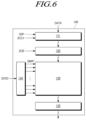
- FIG. 6 is a view schematically illustrating a configuration of a data driving circuit in a display device according to aspects of the present disclosure.
- a data driving circuit 130 may include a shift register 131 , a latch circuit 132 , a gamma circuit 134 , a digital-to-analog converter 133 , and an output buffer 135 .
- the data driving circuit control signal transferred from the timing controller 140 to control the data driving circuit 130 may include a source start pulse SSP, a source sampling clock SCLK, and a source output enable signal SOE.
- the source start pulse SSP controls the data sampling start time of the data driving circuit 130 .
- the source sampling clock SCLK is a clock signal that controls the image data sampling operation in the data driving circuit 130 based on a rising or falling edge.
- the source output enable signal SOE controls the output of the data driving circuit 130 .
- the shift register 131 shifts the image data DATA received as serial data in response to the source start pulse SSP and source sampling clock SCLK transferred from the timing controller 140 and then simultaneously outputs them.
- the image data DATA which is serial data is converted into data of a parallel system which is then supplied to the latch circuit 132 .
- the latch circuit 132 supplies one line of image data DATA to the digital-to-analog converter 133 so that the image data DATA is simultaneously transferred to the source driving integrated circuits SDIC according to the source output enable signal SOE.
- At least two latch circuits 132 may be configured, but for convenience of description, only one latch circuit 132 is shown.
- the gamma circuit 134 generates first to nth gamma reference voltages GMA1-GMAn using the gamma driving power SVDD supplied from the timing controller 140 .
- the digital-to-analog converter 133 converts one line of image data DATA into an analog data voltage Vdata in response to the first to nth gamma reference voltages GMA1-GMAn transferred from the gamma circuit 134 .
- the output buffer 135 amplifies or compensates for the analog data voltage Vdata transferred from the digital-to-analog converter 133 and supplies it to each data line DL.
- the power of the gamma circuit 134 , digital-to-analog converter 133 , and output buffer 135 may be separated from each other and may share one gamma driving power SVDD.
- FIG. 7 is a view illustrating a partial configuration of a data driving circuit in a display device according to aspects of the present disclosure.
- a data driving circuit 130 in a display device 100 may include a gamma circuit 134 , a digital-to-analog converter 133 , and an output buffer 135 .
- the digital-to-analog converter 133 may include a CMOS transistor in which a PMOS transistor and an NMOS transistor are connected in parallel to each other.
- the gamma circuit 134 , the digital-to-analog converter 133 , and the output buffer 135 , which constitute the data driving circuit 130 , may use the gamma driving power SVDD, supplied from the timing controller 140 , as common driving power.
- the driving power applied to the digital-to-analog converter 133 and the output buffer 135 may be applied to a signal line different from that of the gamma driving power SVDD and be supplied with a different level of driving power from that of the gamma driving power SVDD.
- the gamma circuit 134 Since the gamma circuit 134 generates gamma reference voltages GMA corresponding to a plurality of levels (e.g., 256 levels), the gamma circuit 134 generally consumes much current.
- the gamma driving power SVDD may be varied by the timing controller 140 but is not easy to vary by the gamma circuit 134 which consumes much current and is typically fixed to a constant voltage.
- FIG. 8 is a view illustrating an example in which the current of the gamma driving power applied to a data driving circuit is varied due to a transition of image data in a display device according to aspects of the present disclosure.
- the current of the output buffer 135 is increased at the rising or falling edge which appears during the transition of the image data DATA or data voltage Vdata.
- the gamma driving power SVDD supplied to the gamma circuit 134 and output buffer 135 is increased, or so is the current Isvdd supplied to the data driving circuit 130 by the gamma driving power SVDD.
- DDD double-rate driving
- FIG. 9 is a view illustrating an example of a subpixel structure driven in a DRD scheme in a display device according to aspects of the present disclosure.
- the subpixels SP of the display device 100 may include a red subpixel R, a green subpixel G, a blue subpixel B, and a white subpixel W.
- one data line DL is disposed every two columns of subpixels SP, and two gate lines GL may be disposed above and under each row of subpixels SP.
- the white subpixel W and the red subpixel R share one data line DL 11
- the green subpixel G and the blue subpixel B share one data line DL 12 .
- the white subpixel W and the green subpixel G may share the same gate line GL 11 , GL 21 , GL 31 , GL 41 , GL 51 , . . . , and the red subpixel R and the blue subpixel B may share the same gate line GL 12 , GL 22 , GL 32 , GL 42 , . . . .
- subpixel (SP) structure sharing the data line DL and the gate line GL.
- the white subpixel W and the green subpixel G or the red subpixel R and the blue subpixel B may share the data line DL, or the white subpixel W and the red subpixel R may share one gate line GL.
- the data voltage Vdata may be supplied to two subpixels SP through one data line DL during one horizontal period (Horizontal Time), and the gate line GL may be driven at twice as high a frequency as normal driving, applying the scan signal SCAN to each subpixel SP.
- the scan signal SCAN may be controlled so that the data voltage Vdata is alternately applied to the subpixels SP disposed on two opposite sides of one data line DL.
- the display device 100 driven in the DRD scheme may also apply the polarity-inverted data voltage Vdata to each row of subpixels SP to reduce power consumption and minimize flickers. Accordingly, as the data voltage Vdata applied to the subpixel SP, a signal having the same polarity as the data voltage Vdata applied to the previous subpixel SP may be applied, or the polarity-inverted signal may be applied.
- the subpixel SP of the display device 100 may be formed in various structures, and the connection structure between the output buffer 135 of the data driving circuit 130 and the display panel 110 may be changed depending on the structure of the subpixel SP.
- the transition pattern of the image data DATA which increases the temperature of the data driving circuit 130 , may differ depending on the structure of the subpixel SP. As a result, it may be hard to determine the pattern of the image data DATA which increases the temperature of the data driving circuit 130 .
- the display device 100 reduces an increase in the temperature of the data driving circuit 130 by detecting a variation in the gamma driving power SVDD applied to the data driving circuit 130 and accordingly controlling the level or refresh rate of the image data DATA supplied to the data driving circuit 130 from the timing controller 140 .
- FIG. 10 is a system block diagram illustrating a structure of detecting a variation in gamma driving power to thereby control image data in a power management circuit of a display device according to aspects of the present disclosure.
- a display device 100 may include a gamma driving power detection circuit 152 for measuring the gamma driving power SVDD, in the power management circuit 150 which generates various types of driving power.
- the gamma driving power detection circuit 152 may be positioned in the power management circuit 150 and may supply the gamma driving power SVDD, generated by the power management circuit 150 , to the data driving circuit 130 while simultaneously measuring a variation in the gamma driving power SVDD.
- the gamma driving power measurement M_SVDD detected by the gamma driving power detection circuit 152 is transferred to the timing controller 140 .
- the timing controller 140 may change the level or refresh rate of the image data DATA applied to the data driving circuit 130 with respect to the gamma driving power measurement M_SVDD transferred from the power management circuit 150 .
- the timing controller 140 does not change the level or refresh rate of the image data DATA but, if the gamma driving power measurement M_SVDD transferred from the power management circuit 150 exceeds the reference value, the timing controller 140 reduces the level or refresh rate of the image data DATA, suppressing an increase in the temperature of the data driving circuit 130 .
- the timing controller 140 may refer to a lookup table stored in a memory (not shown), extract the compensation value corresponding to the gamma driving power measurement M_SVDD, and apply the extracted compensation value to the image data DATA, thereby changing the level or refresh rate of the image data DATA.
- the target to be changed by the timing controller 140 according to the gamma driving power measurement M_SVDD may be the level of the image data DATA or the refresh rate of the image data DATA.
- the timing controller 140 may simultaneously change the level of the image data DATA and the refresh rate of the image data DATA according to the gamma driving power measurement M_SVDD.
- the timing controller 140 changes the level of the image data DATA applied to the data driving circuit 130 according to the gamma driving power measurement M_SVDD
- the level of the data voltage Vdata supplied from the data driving circuit 130 to the display panel 110 is to be changed according to the level of the image data DATA.
- the timing controller 140 may be regarded as changing the level of the data voltage Vdata supplied to the display panel 110 according to the gamma driving power measurement M_SVDD.
- FIG. 11 is a view illustrating an example of a gamma driving power detection circuit in a display device according to aspects of the present disclosure.
- the gamma driving power detection circuit 152 may include a current sensing resistor Rs, an operational amplifier 154 , and an analog-to-digital converter 156 .
- the current sensing resistor Rs may be connected between the terminal where the gamma driving power SVDD is generated and the data driving circuit 130 , generating a bias voltage according to the current flowing to the line through which the gamma driving power SVDD is supplied to the data driving circuit 130 from the power management circuit 150 .
- the current sensing resistor Rs may have a tiny resistance, e.g., 0.01 ⁇ , to minimize the voltage drop of the gamma driving power SVDD.
- the operational amplifier 154 may be connected between both the ends of the current sensing resistor Rs, sensing and amplifying the bias voltage applied between both the ends of the current sensing resistor Rs. For example, the operational amplifier 154 may amplify the bias voltage applied between both the ends of the current sensing resistor Rs, five times or more.
- the analog-to-digital converter 156 converts the current flowing to the data driving circuit 130 into a digital signal during one frame based on the bias voltage amplified by the operational amplifier 154 , generating the gamma driving power measurement M_SVDD.
- the gamma driving power measurement M_SVDD is provided to the timing controller 140 .
- the timing controller 140 may change the level or refresh rate of the image data DATA transferred to the data driving circuit 130 based on the gamma driving power measurement M_SVDD detected by the power management circuit 150 .
- current is detected by the gamma driving power SVDD, and the current sensing resistor Rs is connected in series between the gamma driving power SVDD and the data driving circuit 130 .
- a signal line transferring the gamma driving power SVDD between the gamma driving power SVDD and the data driving circuit 130 and a dummy channel may be disposed in parallel, and the variation in the voltage of the gamma driving power SVDD may be detected through the dummy channel.
- FIG. 12 is a view illustrating an example in which a level of image data is changed according to a variation in gamma driving power in a display device according to aspects of the present disclosure.
- the display device 100 in the display device 100 according to aspects of the present disclosure, as the area and resolution of the display panel 110 increase, the amount of the image data DATA displayed through the display panel 110 may increase, and the transition of image data DATA may be frequent.
- transition of image data DATA so increases, the temperature of the source driving integrated circuit SDIC supplying the data voltage to the display panel 110 increases, and so does the temperature of the display panel 110 .
- Such phenomenon may be more conspicuous when transition of image data DATA is more frequent, like when the image data is of a game or moving image.
- the timing controller 140 may reduce the high level DATA_H of the image data DATA to correspond to the gamma driving power measurement M_SVDD (the case shown in FIG. 12 ( a ) ) or increase the low level DATA_L of the image data DATA (the case shown in FIG. 12 ( b ) , thereby reducing the level (peak-to-peak value) of the image data DATA.
- FIG. 13 is a view illustrating an example in which a refresh rate of image data is changed according to a variation in gamma driving power in a display device according to aspects of the present disclosure.
- the timing controller 140 may reduce the refresh rate of the image data DATA to correspond to the gamma driving power measurement M_SVDD.
- timing controller 140 reduces the refresh rate of the image data DATA in a state of maintaining the level of the image data DATA constant.
- the timing controller 140 may change both the level of the image data DATA and the refresh rate of the image data DATA according to the gamma driving power measurement M_SVDD.
- the refresh rate may be reduced in the image data DATA changed by the timing controller 140 .
- the refresh rate may be reduced in the image data DATA changed by the timing controller 140 .
- the gamma driving power detection circuit 152 is so disposed in the power management module 150 , the gamma driving power SVDD applied to the data driving circuit 130 may be comprehensively detected and, in this case, the image data DATA may be controlled to correspond to an increase in the temperature of the whole display panel 110 .
- the data driving circuit 130 may include a plurality of source driving integrated circuits SDIC and may measure the variation in the gamma driving power SVDD applied to each source driving integrated circuit SDIC, selecting any source driving integrated circuit SDIC and controlling the image data DATA based on the selected source driving integrated circuit SDIC.
- FIG. 14 is a view illustrating an example of a connection structure of a power management circuit disposed on a control printed circuit board and a plurality of source driving integrated circuits disposed on a source printed circuit board in a display device according to various aspects.
- the gamma driving power SVDD generated from the power management circuit 150 disposed on the control printed circuit board CPCB is transferred to the gamma circuit 134 of the data driving circuit 130 through the source printed circuit board SPCB.
- the gamma circuit 134 voltage-divides the gamma driving power SVDD with a plurality of linear resistors arranged inside the data driving circuit 130 , thereby generating the gamma reference voltages GMA1-GMAn.
- the gamma driving power detection circuit may be disposed in the source driving integrated circuit SDIC.
- the source driving integrated circuit (e.g., SDIC #1) in which the variation in temperature due to a variation in the gamma driving power SVDD is largest may be selected from among the plurality of source driving integrated circuits SDIC #1-SDIC #4, and the level or refresh rate of the image data DATA may be individually controlled with respect to the selected source driving integrated circuit SDIC #1.
- FIG. 15 is a system block diagram illustrating a structure of detecting a variation in gamma driving power to thereby control image data in a data driving circuit of a display device according to aspects of the present disclosure.
- a display device 100 may include a gamma driving power detection circuit 136 for measuring the gamma driving power SVDD, in the data driving circuit 130 which supplies the data voltage Vdata to the display panel 110 .
- the gamma driving power detection circuit 136 may be disposed in the plurality of source driving integrated circuits SDIC constituting the data driving circuit 130 .
- the gamma driving power detection circuit 136 may be positioned in the source driving integrated circuit SDIC to measure the variation in the gamma driving power SVDD transferred from the power management circuit 150 .
- the configuration of the gamma driving power detection circuit 136 may be the same as the configuration illustrated in FIG. 11 .
- the gamma driving power measurement M_SVDD detected by the gamma driving power detection circuit 136 is transferred to the timing controller 140 .
- the timing controller 140 may change the level or refresh rate of the image data DATA applied to the corresponding source driving integrated circuit SDIC with respect to the gamma driving power measurement M_SVDD transferred from the source driving integrated circuit SDIC.
- the timing controller 140 may refer to a lookup table stored in a memory (not shown), extract the compensation value corresponding to the gamma driving power measurement M_SVDD, and apply the extracted compensation value to the image data DATA which is to be supplied to the source driving integrated circuit SDIC, thereby changing the level or refresh rate of the image data DATA.
- FIG. 16 is a flowchart illustrating a display driving method according to aspects of the present disclosure.
- a display driving method may include the step S 100 of detecting gamma driving power SVDD, the step S 200 of comparing a measurement M_SVDD of the gamma driving power with a reference value, the step S 300 of reducing the level of the data voltage Vdata or the step S 400 of reducing the refresh rate of the data voltage Vdata when the gamma driving power measurement M_SVDD exceeds the reference value, and the step S 500 of supplying the changed data voltage Vdata.
- the step S 300 of reducing the level of the data voltage Vdata and the step S 400 of reducing the refresh rate when the gamma driving power measurement M_SVDD exceeds the reference value may be performed simultaneously or only one of the steps may be selectively performed.
- the timing controller 140 may control the level or refresh rate of the image data DATA applied to the data driving circuit 130 , thereby controlling the level or refresh rate of the data voltage Vdata supplied from the data driving circuit 130 to the display panel 110 .
- the display device 100 of the present disclosure may reduce the level or refresh rate of the image data DATA to correspond to the gamma driving power measurement M_SVDD when the gamma driving power measurement M_SVDD exceeds the reference value due to an increase in the transition of image data DATA, thereby suppressing an increase in the temperature of the data driving circuit 130 and enhancing image quality.
- a display device 100 of the present disclosure comprises a display panel 110 where a plurality of gate lines GL, a plurality of data lines DL, and a plurality of subpixels SP are disposed; a gate driving circuit 120 configured to supply a scan signal SCAN to the plurality of gate lines GL; a data driving circuit 130 configured to convert digital image data DATA into an analog data voltage Vdata and supply the analog data voltage Vdata to the plurality of data lines DL; a power management circuit 150 configured to supply a gamma driving power SVDD for driving the data driving circuit 130 to the data driving circuit 130 , and include a gamma driving power detection circuit 152 for detecting the gamma driving power SVDD; and a timing controller 140 configured to control the gate driving circuit 120 and controlling the digital image data DATA supplied to the data driving circuit 130 so that the analog data voltage Vdata supplied to the display panel 110 is changed according to a gamma driving power measurement M_SVDD detected by the gamma driving power detection circuit 152 .
- the gamma driving power SVDD is changed due to transition of the digital image data DATA.
- the data driving circuit 130 includes a shift register 131 configured to convert the digital image data DATA received in a serial form into image data DATA in a parallel form in response to a control signal transferred from the timing controller 140 and output the image data DATA; a latch circuit 132 configured to transfer the image data DATA in the parallel form, on a per-line basis, to be simultaneously supplied to a plurality of source driving integrated circuits SDIC; a gamma circuit 134 configured to generate a plurality of gamma reference voltages GMA using the gamma driving power SVDD; a digital-to-analog converter 133 configured to convert the image data DATA in the parallel form into the analog data voltage Vdata in response to the plurality of gamma reference voltages GMA transferred from the gamma circuit 134 ; and an output buffer 135 configured to supply the analog data voltage Vdata to the plurality of data lines DL.
- a shift register 131 configured to convert the digital image data DATA received in a serial form into image data DATA in
- the gamma driving power SVDD is supplied as a driving voltage of the digital-to-analog converter 133 and the output buffer 135 .
- the gamma driving power detection circuit 152 includes a current sensing resistor Rs connected in series to the gamma driving power SVDD; an operational amplifier 154 connected between two ends of the current sensing resistor Rs to sense a bias voltage; and an analog-to-digital converter 156 configured to convert the bias voltage sensed by the operational amplifier 154 into a digital signal to generate the gamma driving power measurement M_SVDD.
- the timing controller 140 is configured to reduce a level of the digital image data DATA when the gamma driving power measurement M_SVDD exceeds a reference value.
- the timing controller 140 is configured to reduce a high level of the digital image data DATA or increases a low level of the digital image data DATA when the gamma driving power measurement M_SVDD exceeds the reference value.
- the timing controller 140 is configured to reduce a refresh rate of the digital image data DATA when the gamma driving power measurement M_SVDD exceeds a reference value.
- the analog data voltage is changed based on a source driving integrated circuit with a largest variation in the gamma driving power among the plurality of source driving integrated circuits.
- a data driving circuit 130 of the present disclosure comprises a shift register 131 configured to convert digital image data DATA received in a serial form into image data DATA in a parallel form and output the image data DATA; a latch circuit 132 configured to transfer the image data DATA in the parallel form, on a per-line basis, to be simultaneously supplied to a plurality of source driving integrated circuits SDIC; a gamma circuit 134 configured to generate a plurality of gamma reference voltages GMA using gamma driving power SVDD; a digital-to-analog converter 133 configured to convert the image data DATA in the parallel form into an analog data voltage Vdata in response to the plurality of gamma reference voltages GMA transferred from the gamma circuit 134 ; an output buffer 135 configured to supply the analog data voltage Vdata to a display panel 110 through a plurality of data lines DL; and a gamma driving power detection circuit 136 configured to detect the gamma driving power SVDD.
- the gamma driving power SVDD is supplied as a driving voltage of the digital-to-analog converter 133 and the output buffer 135 .
- the gamma driving power detection circuit 136 includes a current sensing resistor Rs connected in series to the gamma driving power SVDD; an operational amplifier 154 connected between two ends of the current sensing resistor Rs to sense a bias voltage; and an analog-to-digital converter 156 configured to convert the bias voltage sensed by the operational amplifier 154 into a digital signal to generate the gamma driving power measurement M_SVDD.
- the analog data voltage Vdata is controlled according to a gamma driving power measurement M_SVDD detected by the gamma driving power detection circuit 136 .
- a level of the analog data voltage Vdata is reduced when the gamma driving power measurement M_SVDD exceeds a reference value.
- a refresh rate of the analog data voltage Vdata is reduced when the gamma driving power measurement M_SVDD exceeds a reference value.
- a method for driving a display device including a display panel where a plurality of gate lines, a plurality of data lines, and a plurality of subpixels are disposed, a gate driving circuit supplying a scan signal to the plurality of gate lines, and a data driving circuit converting digital image data into an analog data voltage and supplying the analog data voltage to the plurality of data lines, comprises detecting gamma driving power supplied to the data driving circuit (S 100 ); comparing a measurement of the gamma driving power with a reference value (S 200 ); controlling the analog data voltage when the gamma driving power measurement exceeds the reference value (S 300 and S 400 ); and supplying the analog data voltage to the display panel (S 500 ).
- Controlling the analog data voltage (S 300 ) includes reducing a level of the analog data voltage Vdata when the gamma driving power measurement exceeds the reference value.
- Controlling the analog data voltage Vdata includes reducing a high level of the analog data voltage Vdata or increasing a low level of the analog data voltage Vdata when the gamma driving power measurement exceeds the reference value.
- Controlling the analog data voltage Vdata includes reducing a refresh rate of the analog data voltage Vdata when the gamma driving power measurement exceeds the reference value.
- the analog data voltage is controlled based on a source driving integrated circuit with a largest variation in the gamma driving power among the plurality of source driving integrated circuits.
Landscapes
- Engineering & Computer Science (AREA)
- Physics & Mathematics (AREA)
- Computer Hardware Design (AREA)
- General Physics & Mathematics (AREA)
- Theoretical Computer Science (AREA)
- Control Of Indicators Other Than Cathode Ray Tubes (AREA)
Abstract
Description
Claims (18)
Applications Claiming Priority (2)
| Application Number | Priority Date | Filing Date | Title |
|---|---|---|---|
| KR10-2021-0099714 | 2021-07-29 | ||
| KR1020210099714A KR102860862B1 (en) | 2021-07-29 | 2021-07-29 | Display device, data driving circuit and display driving method |
Publications (2)
| Publication Number | Publication Date |
|---|---|
| US20230037207A1 US20230037207A1 (en) | 2023-02-02 |
| US11922888B2 true US11922888B2 (en) | 2024-03-05 |
Family
ID=85037816
Family Applications (1)
| Application Number | Title | Priority Date | Filing Date |
|---|---|---|---|
| US17/837,194 Active US11922888B2 (en) | 2021-07-29 | 2022-06-10 | Display device, data driving circuit and display driving method |
Country Status (3)
| Country | Link |
|---|---|
| US (1) | US11922888B2 (en) |
| KR (1) | KR102860862B1 (en) |
| CN (1) | CN115691440A (en) |
Families Citing this family (5)
| Publication number | Priority date | Publication date | Assignee | Title |
|---|---|---|---|---|
| KR20240123904A (en) * | 2023-02-07 | 2024-08-16 | 삼성디스플레이 주식회사 | Data driver and display device having the same |
| KR20250023087A (en) | 2023-08-09 | 2025-02-18 | 주식회사 엘엑스세미콘 | Buffer and data driving device |
| CN120380536A (en) * | 2023-09-27 | 2025-07-25 | 京东方科技集团股份有限公司 | Driving module for display and display device |
| KR20250119312A (en) * | 2024-01-31 | 2025-08-07 | 엘지디스플레이 주식회사 | Display device and integrated driving circuit |
| CN119107891B (en) * | 2024-10-16 | 2025-12-05 | 武汉天马微电子有限公司 | Display panels and their color deviation compensation methods, gamma adjustment methods, and electronic devices |
Citations (10)
| Publication number | Priority date | Publication date | Assignee | Title |
|---|---|---|---|---|
| US20130249969A1 (en) * | 2012-03-23 | 2013-09-26 | Lg Display Co., Ltd. | Liquid crystal display device |
| US8847940B2 (en) * | 2010-02-02 | 2014-09-30 | Samsung Display Co., Ltd. | Display apparatus and method of operating the same |
| US20150145901A1 (en) * | 2013-11-25 | 2015-05-28 | Lg Display Co., Ltd. | Display device and method of driving the same |
| US20150294617A1 (en) * | 2014-04-09 | 2015-10-15 | Samsung Electronics Co., Ltd. | Image data output control apparatus and method using current consumption |
| US20160365058A1 (en) * | 2015-06-11 | 2016-12-15 | Samsung Display Co., Ltd. | Display device |
| US20170076660A1 (en) * | 2015-09-14 | 2017-03-16 | Samsung Display Co., Ltd. | Display device and electronic device having the same |
| US20180211602A1 (en) * | 2017-01-25 | 2018-07-26 | Samsung Display Co., Ltd. | Display device and method of driving the same |
| US20200251045A1 (en) * | 2019-01-31 | 2020-08-06 | Samsung Display Co., Ltd. | Display device |
| US20220051599A1 (en) * | 2020-08-11 | 2022-02-17 | Everdisplay Optronics (Shanghai) Co.,Ltd. | Method and device for driving display panel |
| US20230005411A1 (en) * | 2021-07-05 | 2023-01-05 | Lx Semicon Co., Ltd. | Display device and power management device for supplying power to display device |
Family Cites Families (2)
| Publication number | Priority date | Publication date | Assignee | Title |
|---|---|---|---|---|
| TW201445542A (en) * | 2013-05-20 | 2014-12-01 | Sony Corp | Image signal processing circuit, image signal processing method and display device |
| CN112735348A (en) * | 2020-12-31 | 2021-04-30 | Tcl华星光电技术有限公司 | Driving circuit, driving method and display device |
-
2021
- 2021-07-29 KR KR1020210099714A patent/KR102860862B1/en active Active
-
2022
- 2022-06-10 US US17/837,194 patent/US11922888B2/en active Active
- 2022-06-15 CN CN202210674230.0A patent/CN115691440A/en active Pending
Patent Citations (10)
| Publication number | Priority date | Publication date | Assignee | Title |
|---|---|---|---|---|
| US8847940B2 (en) * | 2010-02-02 | 2014-09-30 | Samsung Display Co., Ltd. | Display apparatus and method of operating the same |
| US20130249969A1 (en) * | 2012-03-23 | 2013-09-26 | Lg Display Co., Ltd. | Liquid crystal display device |
| US20150145901A1 (en) * | 2013-11-25 | 2015-05-28 | Lg Display Co., Ltd. | Display device and method of driving the same |
| US20150294617A1 (en) * | 2014-04-09 | 2015-10-15 | Samsung Electronics Co., Ltd. | Image data output control apparatus and method using current consumption |
| US20160365058A1 (en) * | 2015-06-11 | 2016-12-15 | Samsung Display Co., Ltd. | Display device |
| US20170076660A1 (en) * | 2015-09-14 | 2017-03-16 | Samsung Display Co., Ltd. | Display device and electronic device having the same |
| US20180211602A1 (en) * | 2017-01-25 | 2018-07-26 | Samsung Display Co., Ltd. | Display device and method of driving the same |
| US20200251045A1 (en) * | 2019-01-31 | 2020-08-06 | Samsung Display Co., Ltd. | Display device |
| US20220051599A1 (en) * | 2020-08-11 | 2022-02-17 | Everdisplay Optronics (Shanghai) Co.,Ltd. | Method and device for driving display panel |
| US20230005411A1 (en) * | 2021-07-05 | 2023-01-05 | Lx Semicon Co., Ltd. | Display device and power management device for supplying power to display device |
Also Published As
| Publication number | Publication date |
|---|---|
| KR20230018042A (en) | 2023-02-07 |
| CN115691440A (en) | 2023-02-03 |
| US20230037207A1 (en) | 2023-02-02 |
| KR102860862B1 (en) | 2025-09-16 |
Similar Documents
| Publication | Publication Date | Title |
|---|---|---|
| US11922888B2 (en) | Display device, data driving circuit and display driving method | |
| KR102718034B1 (en) | Display device and method for driving it | |
| US9019187B2 (en) | Liquid crystal display device including TFT compensation circuit | |
| CN116092440B (en) | Display device and driving circuit | |
| US11769445B2 (en) | Multiplexer circuit, multiplexer, driving method, display panel, and display apparatus | |
| US11854495B2 (en) | Display device and display driving method | |
| CN116110335B (en) | Display device, display panel, and display driving method | |
| US12027102B2 (en) | Display device and display driving method | |
| KR102887004B1 (en) | Display device and display driving method | |
| CN116363987B (en) | Sub-pixel circuit, display panel and display device | |
| US20230068639A1 (en) | Display device, data driving circuit and display driving method | |
| US11862057B2 (en) | Gate driver and display device using the same | |
| US11430395B2 (en) | Display device and driving circuit | |
| US20250239223A1 (en) | Display device and driving method thereof | |
| US20250148982A1 (en) | Display device, driving circuit, and display driving method | |
| KR20250049671A (en) | Compensation circuit and display device including the same | |
| KR20230034823A (en) | Pixel circuit and display device including the same | |
| US20250157415A1 (en) | Display device and display driving method | |
| US12412526B2 (en) | Pixel circuit and display device including the same | |
| US12494171B2 (en) | Subpixel circuit, display panel and display device | |
| KR20250132677A (en) | Display Apparatus | |
| KR20250080191A (en) | Method of contralling ripple of cathode voltage and display device using the same | |
| KR20230009261A (en) | Pixel circuit and display device including the same |
Legal Events
| Date | Code | Title | Description |
|---|---|---|---|
| AS | Assignment |
Owner name: LG DISPLAY CO., LTD., KOREA, REPUBLIC OF Free format text: ASSIGNMENT OF ASSIGNORS INTEREST;ASSIGNOR:HONG, MOOKYOUNG;REEL/FRAME:060335/0258 Effective date: 20220610 |
|
| FEPP | Fee payment procedure |
Free format text: ENTITY STATUS SET TO UNDISCOUNTED (ORIGINAL EVENT CODE: BIG.); ENTITY STATUS OF PATENT OWNER: LARGE ENTITY |
|
| STPP | Information on status: patent application and granting procedure in general |
Free format text: DOCKETED NEW CASE - READY FOR EXAMINATION |
|
| STPP | Information on status: patent application and granting procedure in general |
Free format text: RESPONSE TO NON-FINAL OFFICE ACTION ENTERED AND FORWARDED TO EXAMINER |
|
| STPP | Information on status: patent application and granting procedure in general |
Free format text: FINAL REJECTION MAILED |
|
| STPP | Information on status: patent application and granting procedure in general |
Free format text: RESPONSE AFTER FINAL ACTION FORWARDED TO EXAMINER |
|
| STPP | Information on status: patent application and granting procedure in general |
Free format text: NOTICE OF ALLOWANCE MAILED -- APPLICATION RECEIVED IN OFFICE OF PUBLICATIONS |
|
| STPP | Information on status: patent application and granting procedure in general |
Free format text: PUBLICATIONS -- ISSUE FEE PAYMENT VERIFIED |
|
| STCF | Information on status: patent grant |
Free format text: PATENTED CASE |