US11894469B2 - Resonant tunneling devices including two-dimensional semiconductor materials and methods of detecting physical properties using the same - Google Patents
Resonant tunneling devices including two-dimensional semiconductor materials and methods of detecting physical properties using the same Download PDFInfo
- Publication number
- US11894469B2 US11894469B2 US16/811,549 US202016811549A US11894469B2 US 11894469 B2 US11894469 B2 US 11894469B2 US 202016811549 A US202016811549 A US 202016811549A US 11894469 B2 US11894469 B2 US 11894469B2
- Authority
- US
- United States
- Prior art keywords
- dimensional semiconductor
- resonant tunneling
- tunneling device
- semiconductor material
- semiconductor layer
- Prior art date
- Legal status (The legal status is an assumption and is not a legal conclusion. Google has not performed a legal analysis and makes no representation as to the accuracy of the status listed.)
- Active, expires
Links
Images


Classifications
-
- H01L29/882—
-
- H—ELECTRICITY
- H10—SEMICONDUCTOR DEVICES; ELECTRIC SOLID-STATE DEVICES NOT OTHERWISE PROVIDED FOR
- H10D—INORGANIC ELECTRIC SEMICONDUCTOR DEVICES
- H10D62/00—Semiconductor bodies, or regions thereof, of devices having potential barriers
- H10D62/10—Shapes, relative sizes or dispositions of the regions of the semiconductor bodies; Shapes of the semiconductor bodies
-
- H—ELECTRICITY
- H10—SEMICONDUCTOR DEVICES; ELECTRIC SOLID-STATE DEVICES NOT OTHERWISE PROVIDED FOR
- H10N—ELECTRIC SOLID-STATE DEVICES NOT OTHERWISE PROVIDED FOR
- H10N80/00—Bulk negative-resistance effect devices
- H10N80/01—Manufacture or treatment
-
- G—PHYSICS
- G01—MEASURING; TESTING
- G01D—MEASURING NOT SPECIALLY ADAPTED FOR A SPECIFIC VARIABLE; ARRANGEMENTS FOR MEASURING TWO OR MORE VARIABLES NOT COVERED IN A SINGLE OTHER SUBCLASS; TARIFF METERING APPARATUS; MEASURING OR TESTING NOT OTHERWISE PROVIDED FOR
- G01D5/00—Mechanical means for transferring the output of a sensing member; Means for converting the output of a sensing member to another variable where the form or nature of the sensing member does not constrain the means for converting; Transducers not specially adapted for a specific variable
- G01D5/12—Mechanical means for transferring the output of a sensing member; Means for converting the output of a sensing member to another variable where the form or nature of the sensing member does not constrain the means for converting; Transducers not specially adapted for a specific variable using electric or magnetic means
- G01D5/14—Mechanical means for transferring the output of a sensing member; Means for converting the output of a sensing member to another variable where the form or nature of the sensing member does not constrain the means for converting; Transducers not specially adapted for a specific variable using electric or magnetic means influencing the magnitude of a current or voltage
-
- H01L29/045—
-
- H01L29/0657—
-
- H01L29/1606—
-
- H01L29/24—
-
- H01L29/267—
-
- H01L29/417—
-
- H01L29/66977—
-
- H01L31/032—
-
- H—ELECTRICITY
- H10—SEMICONDUCTOR DEVICES; ELECTRIC SOLID-STATE DEVICES NOT OTHERWISE PROVIDED FOR
- H10D—INORGANIC ELECTRIC SEMICONDUCTOR DEVICES
- H10D10/00—Bipolar junction transistors [BJT]
- H10D10/80—Heterojunction BJTs
- H10D10/821—Vertical heterojunction BJTs
- H10D10/881—Resonant tunnelling transistors
-
- H—ELECTRICITY
- H10—SEMICONDUCTOR DEVICES; ELECTRIC SOLID-STATE DEVICES NOT OTHERWISE PROVIDED FOR
- H10D—INORGANIC ELECTRIC SEMICONDUCTOR DEVICES
- H10D48/00—Individual devices not covered by groups H10D1/00 - H10D44/00
- H10D48/383—Quantum effect devices, e.g. of devices using quantum reflection, diffraction or interference effects
-
- H—ELECTRICITY
- H10—SEMICONDUCTOR DEVICES; ELECTRIC SOLID-STATE DEVICES NOT OTHERWISE PROVIDED FOR
- H10D—INORGANIC ELECTRIC SEMICONDUCTOR DEVICES
- H10D62/00—Semiconductor bodies, or regions thereof, of devices having potential barriers
- H10D62/10—Shapes, relative sizes or dispositions of the regions of the semiconductor bodies; Shapes of the semiconductor bodies
- H10D62/117—Shapes of semiconductor bodies
-
- H—ELECTRICITY
- H10—SEMICONDUCTOR DEVICES; ELECTRIC SOLID-STATE DEVICES NOT OTHERWISE PROVIDED FOR
- H10D—INORGANIC ELECTRIC SEMICONDUCTOR DEVICES
- H10D62/00—Semiconductor bodies, or regions thereof, of devices having potential barriers
- H10D62/40—Crystalline structures
- H10D62/405—Orientations of crystalline planes
-
- H—ELECTRICITY
- H10—SEMICONDUCTOR DEVICES; ELECTRIC SOLID-STATE DEVICES NOT OTHERWISE PROVIDED FOR
- H10D—INORGANIC ELECTRIC SEMICONDUCTOR DEVICES
- H10D62/00—Semiconductor bodies, or regions thereof, of devices having potential barriers
- H10D62/80—Semiconductor bodies, or regions thereof, of devices having potential barriers characterised by the materials
- H10D62/82—Heterojunctions
-
- H—ELECTRICITY
- H10—SEMICONDUCTOR DEVICES; ELECTRIC SOLID-STATE DEVICES NOT OTHERWISE PROVIDED FOR
- H10D—INORGANIC ELECTRIC SEMICONDUCTOR DEVICES
- H10D62/00—Semiconductor bodies, or regions thereof, of devices having potential barriers
- H10D62/80—Semiconductor bodies, or regions thereof, of devices having potential barriers characterised by the materials
- H10D62/881—Semiconductor bodies, or regions thereof, of devices having potential barriers characterised by the materials being a two-dimensional material
- H10D62/882—Graphene
-
- H—ELECTRICITY
- H10—SEMICONDUCTOR DEVICES; ELECTRIC SOLID-STATE DEVICES NOT OTHERWISE PROVIDED FOR
- H10D—INORGANIC ELECTRIC SEMICONDUCTOR DEVICES
- H10D64/00—Electrodes of devices having potential barriers
- H10D64/20—Electrodes characterised by their shapes, relative sizes or dispositions
- H10D64/23—Electrodes carrying the current to be rectified, amplified, oscillated or switched, e.g. sources, drains, anodes or cathodes
-
- H—ELECTRICITY
- H10—SEMICONDUCTOR DEVICES; ELECTRIC SOLID-STATE DEVICES NOT OTHERWISE PROVIDED FOR
- H10D—INORGANIC ELECTRIC SEMICONDUCTOR DEVICES
- H10D8/00—Diodes
- H10D8/70—Tunnel-effect diodes
- H10D8/755—Resonant tunneling diodes [RTD]
-
- H—ELECTRICITY
- H10—SEMICONDUCTOR DEVICES; ELECTRIC SOLID-STATE DEVICES NOT OTHERWISE PROVIDED FOR
- H10F—INORGANIC SEMICONDUCTOR DEVICES SENSITIVE TO INFRARED RADIATION, LIGHT, ELECTROMAGNETIC RADIATION OF SHORTER WAVELENGTH OR CORPUSCULAR RADIATION
- H10F77/00—Constructional details of devices covered by this subclass
- H10F77/10—Semiconductor bodies
- H10F77/12—Active materials
-
- H—ELECTRICITY
- H10—SEMICONDUCTOR DEVICES; ELECTRIC SOLID-STATE DEVICES NOT OTHERWISE PROVIDED FOR
- H10N—ELECTRIC SOLID-STATE DEVICES NOT OTHERWISE PROVIDED FOR
- H10N80/00—Bulk negative-resistance effect devices
-
- H—ELECTRICITY
- H10—SEMICONDUCTOR DEVICES; ELECTRIC SOLID-STATE DEVICES NOT OTHERWISE PROVIDED FOR
- H10P—GENERIC PROCESSES OR APPARATUS FOR THE MANUFACTURE OR TREATMENT OF DEVICES COVERED BY CLASS H10
- H10P14/00—Formation of materials, e.g. in the shape of layers or pillars
- H10P14/20—Formation of materials, e.g. in the shape of layers or pillars of semiconductor materials
- H10P14/34—Deposited materials, e.g. layers
- H10P14/3402—Deposited materials, e.g. layers characterised by the chemical composition
- H10P14/3436—Deposited materials, e.g. layers characterised by the chemical composition being chalcogenide semiconductor materials not being oxides, e.g. ternary compounds
-
- H—ELECTRICITY
- H10—SEMICONDUCTOR DEVICES; ELECTRIC SOLID-STATE DEVICES NOT OTHERWISE PROVIDED FOR
- H10P—GENERIC PROCESSES OR APPARATUS FOR THE MANUFACTURE OR TREATMENT OF DEVICES COVERED BY CLASS H10
- H10P14/00—Formation of materials, e.g. in the shape of layers or pillars
- H10P14/40—Formation of materials, e.g. in the shape of layers or pillars of conductive or resistive materials
- H10P14/418—Formation of materials, e.g. in the shape of layers or pillars of conductive or resistive materials the conductive layers comprising transition metals
-
- H—ELECTRICITY
- H10—SEMICONDUCTOR DEVICES; ELECTRIC SOLID-STATE DEVICES NOT OTHERWISE PROVIDED FOR
- H10P—GENERIC PROCESSES OR APPARATUS FOR THE MANUFACTURE OR TREATMENT OF DEVICES COVERED BY CLASS H10
- H10P74/00—Testing or measuring during manufacture or treatment of wafers, substrates or devices
- H10P74/20—Testing or measuring during manufacture or treatment of wafers, substrates or devices characterised by the properties tested or measured, e.g. structural or electrical properties
- H10P74/203—Structural properties, e.g. testing or measuring thicknesses, line widths, warpage, bond strengths or physical defects
-
- H—ELECTRICITY
- H10—SEMICONDUCTOR DEVICES; ELECTRIC SOLID-STATE DEVICES NOT OTHERWISE PROVIDED FOR
- H10P—GENERIC PROCESSES OR APPARATUS FOR THE MANUFACTURE OR TREATMENT OF DEVICES COVERED BY CLASS H10
- H10P74/00—Testing or measuring during manufacture or treatment of wafers, substrates or devices
- H10P74/20—Testing or measuring during manufacture or treatment of wafers, substrates or devices characterised by the properties tested or measured, e.g. structural or electrical properties
- H10P74/207—Electrical properties, e.g. testing or measuring of resistance, deep levels or capacitance-voltage characteristics
-
- B—PERFORMING OPERATIONS; TRANSPORTING
- B82—NANOTECHNOLOGY
- B82Y—SPECIFIC USES OR APPLICATIONS OF NANOSTRUCTURES; MEASUREMENT OR ANALYSIS OF NANOSTRUCTURES; MANUFACTURE OR TREATMENT OF NANOSTRUCTURES
- B82Y10/00—Nanotechnology for information processing, storage or transmission, e.g. quantum computing or single electron logic
Definitions
- the present disclosure relates to resonant tunneling devices including one or more two-dimensional semiconductor materials and methods of detecting physical properties using the resonant tunneling devices.
- the negative differential resistance (NDR) effect is a phenomenon in which current through a device decreases even though voltage applied to the device increases.
- the NDR effect is generally found in bulk-type materials having non-linear electrical properties and is applied in various fields such amplifiers, electronic oscillators, digital analog converters, switching circuits, memories, or the like. Meanwhile, the NDR effect has been recently observed in resonant tunneling devices manufactured by bonding two-dimensional materials.
- resonant tunneling devices including a two-dimensional semiconductor material and methods of detecting physical properties using the resonant tunneling devices.
- a resonant tunneling device may include a first two-dimensional semiconductor layer including a first two-dimensional semiconductor material, a first insulating layer on the first two-dimensional semiconductor layer, and a second two-dimensional semiconductor layer on the first insulating layer, the second two-dimensional semiconductor layer including a second two-dimensional semiconductor material of a same kind as the first two-dimensional semiconductor material.
- a crystal lattice of the first two-dimensional semiconductor material and a crystal lattice of the second two-dimensional semiconductor material may be aligned with each other.
- the first two-dimensional semiconductor material and the second two-dimensional semiconductor material may each include transition metal dichalcogenide (TMD).
- TMD transition metal dichalcogenide
- the TMD may be expressed by ⁇ Equation 1>, M 1-a M a ′X 2(1-b) X 2b ′ ⁇ Equation 1> wherein, in ⁇ Equation 1>, M and M′ are different transition metal elements, X and X′ are different chalcogen elements, 0 ⁇ a ⁇ 1, and 0 ⁇ b ⁇ 1.
- the different transition metal elements may each include a different at least one of Ti, Zr, Hf, V, Nb, Ta, Mo, W, Tc, Re, Co, Rh, Ir, Ni, Pd, Pt, Zn, or Sn, and the different chalcogen elements may each include a different at least one of S, Se or Te.
- the first insulating layer may include a two-dimensional insulating material or an oxide material.
- the resonant tunneling device may further include a first electrode electrically connected to the first two-dimensional semiconductor layer, and a second electrode electrically connected to the second two-dimensional semiconductor layer.
- the resonant tunneling device may further include a substrate, wherein the first two-dimensional semiconductor layer is on the substrate.
- the substrate may include an insulating material.
- the resonant tunneling device may further include a second insulating layer, wherein the first two-dimensional semiconductor layer is on the second insulating layer; and a substrate, wherein the second insulating layer is on the substrate and includes an electrically conductive material.
- the substrate may serve as a gate electrode, and the second insulating layer may serve as a gate insulating layer.
- the resonant tunneling device may further include a graphene layer on at least one of the first two-dimensional semiconductor layer or the second two-dimensional semiconductor layer.
- the resonant tunneling device may be configured to detect one or more physical properties of the first two-dimensional semiconductor material and the second two-dimensional semiconductor material based on a negative differential resistance (NDR) effect.
- NDR negative differential resistance
- the physical properties may include an electronic structure, a bandgap, or a quantum capacitance.
- the resonant tunneling device may be configured to detect a temperature, a wavelength of light or an intensity of light based on the NDR effect.
- a method of detecting physical properties using a resonant tunneling device that includes a first two-dimensional semiconductor layer, the first two-dimensional semiconductor layer including a first two-dimensional semiconductor material, a first insulating layer on the first two-dimensional semiconductor layer, and a second two-dimensional semiconductor layer on the first insulating layer and including a second two-dimensional semiconductor material of a same kind as the first two-dimensional semiconductor material, wherein a crystal lattice of the first two-dimensional semiconductor material and a crystal lattice of the second two-dimensional semiconductor material are aligned with each other, may include causing the resonant tunneling device to detect one or more physical properties of the first and second two-dimensional semiconductor materials, based on a negative differential resistance (NDR) effect.
- NDR negative differential resistance
- the physical properties may include an electronic structure, a bandgap, or a quantum capacitance.
- the physical properties may be the bandgap, and the bandgap may be detected using the NDR effect generated according to a gate voltage in the resonant tunneling device.
- a method of detecting physical properties using a resonant tunneling device that includes a first two-dimensional semiconductor layer, the first two-dimensional semiconductor layer including a first two-dimensional semiconductor material; a first insulating layer on the first two-dimensional semiconductor layer; and a second two-dimensional semiconductor layer provided on the first insulating layer and including a second two-dimensional semiconductor material of a same kind as the first two-dimensional semiconductor material, wherein a crystal lattice of the first two-dimensional semiconductor material and a crystal lattice of the second two-dimensional semiconductor material are aligned with each other, may include causing the resonant tunneling device to detect one or more of a temperature, a wavelength of light incident on the resonant tunneling device, or an intensity of the light incident on the resonant tunneling device, based on a negative differential resistance (NDR) effect.
- NDR negative differential resistance
- the temperature may be detected using the NDR effect generated according to the temperature in the resonant tunneling device.
- the wavelength of the light or the intensity of the light may be detected using the NDR effect generated according to the light incident on the resonant tunneling device.
- a resonant tunneling device may include a first two-dimensional semiconductor layer including a first two-dimensional semiconductor material, a first insulating layer on the first two-dimensional semiconductor layer, and a second two-dimensional semiconductor layer on the insulating layer, the second two-dimensional semiconductor layer including a second two-dimensional semiconductor material of a same kind as the first two-dimensional semiconductor material.
- a crystal lattice of the first two-dimensional semiconductor material and a crystal lattice of the second two-dimensional semiconductor material may be aligned with each other.
- the first two-dimensional semiconductor material and the second two-dimensional semiconductor material may each include transition metal dichalcogenide (TMD).
- TMD transition metal dichalcogenide
- the TMD may be expressed by ⁇ Equation 1>, M 1-a M a ′X 2(1-b) X 2b ′ ⁇ Equation 1> wherein, in ⁇ Equation 1>, M and M′ are different transition metal elements, X and X′ are different chalcogen elements, 0 ⁇ a ⁇ 1, and 0 ⁇ b ⁇ 1.
- the different transition metal elements may each include a different at least one of Ti, Zr, Hf, V, Nb, Ta, Mo, W, Tc, Re, Co, Rh, Ir, Ni, Pd, Pt, Zn, or Sn, and the different chalcogen elements may each include a different at least one of S, Se or Te.
- the first insulating layer may include a two-dimensional insulating material or an oxide material.
- the resonant tunneling device may further include a first electrode electrically connected to the first two-dimensional semiconductor layer, and a second electrode electrically connected to the second two-dimensional semiconductor layer.
- the resonant tunneling device may further include a substrate, wherein the first two-dimensional semiconductor layer is on the substrate.
- the substrate may include an insulating material.
- the resonant tunneling device may further include a second insulating layer, wherein the first two-dimensional semiconductor layer is on the second insulating layer; and a substrate, wherein the second insulating layer is on the substrate and includes an electrically conductive material.
- the substrate may serve as a gate electrode, and the second insulating layer may serve as a gate insulating layer.
- the resonant tunneling device may further include a graphene layer on at least one of the first two-dimensional semiconductor layer or the second two-dimensional semiconductor layer.
- a system may include the resonant tunneling device, a power supply, and processing circuitry configured to control an application of voltage to at least one of the first two-dimensional semiconductor layer or the second two-dimensional semiconductor layer of the resonant tunneling device to cause the resonant tunneling device to perform at least one of detecting one or more physical properties of the first and second two-dimensional semiconductor materials, based on a negative differential resistance (NDR) effect, or detecting one or more of a temperature, a wavelength of light incident on the resonant tunneling device, or an intensity of the light incident on the resonant tunneling device, based on a negative differential resistance (NDR) effect.
- NDR negative differential resistance
- FIG. 1 shows a resonant tunneling device according to some example embodiments
- FIG. 2 A is a schematic plan view of a state in which a crystal lattice of a first two-dimensional semiconductor material and a crystal lattice of a second two-dimensional semiconductor material are not aligned;
- FIG. 2 B is a schematic plan view of a state in which a crystal lattice of a first two-dimensional semiconductor material and a crystal lattice of a second two-dimensional semiconductor material are aligned with each other;
- FIGS. 3 A, 3 B, 3 C, and 3 D illustrate resonant tunneling and an NDR effect according to voltage applied between first and second electrodes in the resonant tunneling device according to some example embodiments;
- FIG. 4 shows a voltage-current property curve with respect to a gate voltage of a general resonant tunneling device
- FIG. 5 shows a voltage-current property curve with respect to a gate voltage of a resonant tunneling device according to some example embodiments
- FIG. 6 shows a voltage-current property curve of a resonant tunneling device with respect to temperature according to some example embodiments
- FIG. 7 shows a voltage-current property curve with respect to power of incident light of a resonant tunneling device according to some example embodiments
- FIG. 8 shows a response property of a resonant tunneling device with respect to incident light according to some example embodiments
- FIG. 9 shows an external quantum efficiency of a resonant tunneling device with respect to incident light according to some example embodiments
- FIG. 10 shows a resonant tunneling device according to some example embodiments
- FIG. 11 shows a resonant tunneling device according to some example embodiments
- FIG. 12 shows a resonant tunneling device according to some example embodiments
- FIG. 13 shows a resonant tunneling device according to some example embodiments
- FIGS. 14 and 15 are flowcharts that illustrate methods of operating a resonant tunneling device according to some example embodiments.
- FIGS. 16 , 17 , 18 , and 19 show resonant tunneling devices according to some example embodiments.
- FIG. 20 shows a schematic of a system configured to control and monitor the application of voltage to various elements of a resonant tunneling device according to some example embodiments.
- FIG. 1 shows a resonant tunneling device 100 according to some example embodiments.
- a resonant tunneling device may be referred to as a “semiconductor device”.
- the resonant tunneling device 100 may include a substrate 110 , a first two-dimensional semiconductor layer 131 , a first insulating layer 140 , a second two-dimensional semiconductor layer 132 and a graphene layer 150 that are sequentially stacked on the substrate 110 .
- the substrate 110 may be omitted.
- an element that is “on” another element may be above or beneath the other element. Additionally, an element that is “on” another element may be directly on the other element, such that the element is in direct contact with the other element, or may be indirectly on the other element, such that the element is isolated from direct contact with the other element by one or more interposing spaces and/or structures.
- the substrate 110 may include a conductive material, for example an electrically conductive material.
- the substrate 110 may serve as a gate electrode.
- the substrate 110 may include a semiconductor material.
- the semiconductor material may include, for example, a Group IV semiconductor material or a semiconductor compound.
- the Group IV semiconductor material may include Si, Ge, Sn, or the like.
- the substrate 110 may include metal.
- the metal may include, for example, at least one of Cu, Mo, Ni, Al, W, Ru, Co, Mn, Ti, Ta, Au, Hf, Zr, Zn, Y, Cr or Gd.
- the materials of the substrate 110 mentioned above are merely examples, and the substrate 110 may include other various materials.
- the substrate 110 may include an insulating material.
- a second insulating layer 120 may be formed on an upper surface 110 a of the substrate 110 , such that the first two-dimensional semiconductor layer 132 is on the second insulating layer 120 and that the second insulating layer 120 is on the substrate 110 .
- the second insulating layer 120 may serve as a gate insulating layer.
- the second insulating layer 120 may include, for example, oxide (“an oxide material”) or nitride (“a nitride material”), but is not limited thereto.
- the second insulating layer 120 may be omitted from the resonant tunneling device 100 .
- the first two-dimensional semiconductor layer 131 including a first two-dimensional semiconductor material may be provided on an upper surface 120 a of the second insulating layer 120 . It will be understood that the first two-dimensional semiconductor layer 131 is on the substrate 110 .
- the two-dimensional semiconductor material refers to a material having a two-dimensional crystal structure and having a semiconductor property.
- the first two-dimensional semiconductor material may include, for example, transition metal dichalcogenide (TMD).
- TMD is a two-dimensional material having semiconductor properties, and has excellent electrical properties. Even when a thickness of TMD is reduced to nanoscale, its characteristics do not change greatly and TMD has high mobility and thus applied to various devices.
- TMD may include two chalcogen atomic layers having a two-dimensional hexagonal honeycomb structure and one metal atomic layer sandwiched between the two chalcogen atomic layers.
- TMD may be expressed by ⁇ Equation 1> as shown below.
- M and M′ are different transition metal elements
- X and X′ are different chalcogen elements, 0 ⁇ a ⁇ 1, and 0 ⁇ b ⁇ 1.
- the different transition metal elements M and M′ may each include a different at least one of Ti, Zr, Hf, V, Nb, Ta, Mo, W, Tc, Re, Co, Rh, Ir, Ni, Pd, Pt, Zn, or Sn.
- the different chalcogen elements X and X′ may each include a different at least one of S, Se, or Te. However, the chalcogen element is not limited thereto.
- the first insulating layer 140 may be formed on the upper surface 131 a of the first two-dimensional semiconductor layer 131 , such that the first insulating layer 140 is understood to be on the first two-dimensional semiconductor layer 131 .
- the first insulating layer 140 may include, for example, a two-dimensional insulating material.
- the two-dimensional semiconductor material means a material having a two-dimensional crystal structure and having an insulating property.
- the two-dimensional insulating material may include, for example, hexagonal boron nitride (h-BN).
- h-BN hexagonal boron nitride
- the two-dimensional insulating material is not limited thereto.
- the first insulating layer 140 may include an insulating material that is different from the two-dimensional insulating material.
- the first insulating layer 140 may include an oxide material (also referred to herein as simply “oxide”) or the like.
- a second two-dimensional semiconductor layer 132 including the second two-dimensional semiconductor material may be formed on an upper surface 140 a of the first insulating layer 140 , such that the second two-dimensional semiconductor layer 132 is on the first insulating layer 140 .
- the second two-dimensional semiconductor material may be a same kind of material as the first two-dimensional semiconductor material described above. It will be understood that a material that is a “same kind” as another material may be a same type, composition, category, or the like of material as the other material.
- the second two-dimensional semiconductor material may include TMD, such that the first two-dimensional semiconductor layer 131 material and the second two-dimensional semiconductor layer 132 material each include the aforementioned TMD and thus the second two-dimensional semiconductor layer 132 material includes a same kind of material as the first two-dimensional semiconductor layer 131 material.
- the second two-dimensional semiconductor material may be disposed on the first insulating layer 140 such that a crystal lattice of the first two-dimensional semiconductor material of the first two-dimensional semiconductor layer 131 and a crystal lattice of the second two-dimensional semiconductor material of the second two-dimensional semiconductor layer 132 are aligned with each other.
- two separate crystal lattices are “aligned” with each other where the crystal lattices are at least 90% aligned with each other.
- a crystal lattice of the first two-dimensional semiconductor material of the first two-dimensional semiconductor layer 131 and a crystal lattice of the second two-dimensional semiconductor material of the second two-dimensional semiconductor layer 132 are not aligned with each other (e.g., are more that 10% out of alignment with each other).
- FIG. 2 A illustrates a state in which a crystal lattice 131 ′ of the first two-dimensional semiconductor material and a crystal lattice 132 ′ of the second two-dimensional semiconductor material are not aligned.
- the crystal lattice 132 ′ of the second two-dimensional semiconductor material may be twisted by a certain angle with the crystal lattice 131 ′ of the first two-dimensional semiconductor material.
- FIG. 2 B illustrates a state in which the crystal lattice 131 ′ of the first two-dimensional semiconductor material and the crystal lattice 132 ′ of the second two-dimensional semiconductor material are aligned with each other.
- the first and second two-dimensional semiconductor layers 131 and 132 including the first and second two-dimensional semiconductor materials of the same kind may be provided with the first insulating layer 140 therebetween.
- the crystal lattice 131 ′ of the first two-dimensional semiconductor material and the crystal lattice 132 ′ of the second two-dimensional semiconductor material may be aligned with each other.
- the alignment of the crystal lattice 131 ′ of the first two-dimensional semiconductor material and the crystal lattice 132 ′ of the second two-dimensional semiconductor material may be performed by using, for example, a transfer method.
- the resonant tunneling device 100 By aligning the crystal lattice 131 ′ of the first two-dimensional semiconductor material with the crystal lattice 132 ′ of the second two-dimensional semiconductor material, the resonant tunneling device 100 , in which resonant tunneling and a negative differential resistance (NDR) effect more clearly appear, may be manufactured as will be described later.
- NDR effect refers to a phenomenon in which current decreases even though voltage applied to a device increases.
- the graphene layer 150 including graphene may be provided on an upper surface 132 a of the second two-dimensional semiconductor layer 132 .
- Graphene is a material having a two-dimensional crystal structure and having a conductive property.
- graphene is a material having a hexagonal honeycomb structure in which carbon atoms are two-dimensionally connected, and has a very small thickness of an atomic size level.
- Graphene has high electrical mobility and excellent thermal property, chemical stability, and a wide surface area.
- the graphene layer 150 may facilitate the flow of electrons and holes by easily adjusting the chemical potential of a second electrode 172 , which will be described later.
- the first two-dimensional semiconductor layer 131 may be electrically connected to a first electrode 171
- the second two-dimensional semiconductor layer 132 may be electrically connected to the second electrode 172 through the graphene layer 150
- a third insulating layer 160 may be formed to cover an upper surface 131 a of the first two-dimensional semiconductor layer 131 and an upper surface 150 a of the graphene layer 150 exposed to the outside.
- the first electrode 171 may be formed on the third insulating layer 160 to be connected to the first two-dimensional semiconductor layer 131 through a via hole 161 - 1 formed in the third insulating layer 160 .
- the second electrode 172 may be provided on the third insulating layer 160 and be connected to the graphene layer 150 through another via hole 161 - 2 formed in the third insulating layer 160 . It will be understood that, in some example embodiments, the third insulating layer 160 may be omitted from the resonant tunneling device 100 .
- the first electrode 171 may be a source electrode, and the second electrode 172 may be a drain electrode.
- the first and second electrodes 171 and 172 may include, for example, metal having excellent conductivity.
- the metal may include at least one of Cu, Mo, Ni, Al, W, Ru, Co, Mn, Ti, Ta, Au, Hf, Zr, Zn, Y, Cr or Gd.
- the metal is not limited thereto.
- the first electrode 171 and/or the second electrode 172 may be omitted from the resonant tunneling device 100 .
- FIGS. 3 A, 3 B, 3 C, and 3 D illustrate resonant tunneling and an NDR effect according to voltage applied between the first and second electrodes 171 and 172 in the resonant tunneling device 100 according to some example embodiments shown in FIG. 1 .
- MoS 2 is used as first and second two-dimensional semiconductor materials, and a crystal lattice of MoS 2 , which is the first two-dimensional semiconductor material, and a crystal lattice of MoS 2 , which is the second two-dimensional semiconductor material, are arranged in alignment with each other.
- h-BN is used as a material of the first insulating layer 140 provided between the first and second two-dimensional semiconductor layers 131 and 132 . Silicon and silicon oxide are used as the substrate 110 and the second insulating layer 120 material, respectively.
- FIGS. 3 A through 3 D an energy band diagram of MoS 2 , which is the first two-dimensional semiconductor material, is shown on the left side of h-BN, which is the material of the first insulating layer 140 and an energy band diagram of MoS 2 , which is the second two-dimensional semiconductor material, is shown on the right side of h-BN.
- V g denotes a particular (or, alternatively, predetermined) gate voltage applied to the substrate 110
- V d denotes a voltage applied between the first and second two-dimensional semiconductor layers 131 and 132 (e.g., between the first electrode 171 and the second electrode 172 ).
- V R represents a resonant voltage at which resonant tunneling occurs.
- the resonant tunneling and the NDR effect may more clearly appear than when crystal lattices are not aligned.
- crystal lattice of MoS 2 which is the first two-dimensional semiconductor material
- crystal lattice of MoS 2 which is the second two-dimensional semiconductor material
- the resonant tunneling device 100 may effectively detect material properties of a two-dimensional semiconductor material such as an electronic structure, a bandgap, or a quantum capacitance by using resonant tunneling and the NDR effect. Also, the resonant tunneling device 100 according to some example embodiments may effectively detect the temperature therearound or the wavelength or intensity of light applied thereto.
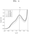
- FIG. 4 shows a voltage-current property curve with respect to a gate voltage of a general resonant tunneling device.
- the general resonant tunneling device has the same structure as the resonant tunneling device 100 shown in FIG. 1 , except that a crystal lattice of a first two-dimensional semiconductor material and a crystal lattice of a second two-dimensional semiconductor material are not aligned.
- MoS 2 is used as the first and second two-dimensional semiconductor materials
- h-BN is used as a first insulating layer material provided between first and second two-dimensional semiconductor layers. Silicon and silicon oxide are used as a substrate and a second insulating layer material, respectively.
- the resonant tunneling and NDR effect may appear in the general resonant tunneling device.
- a resonant voltage at which resonant tunneling occurs is constant even though a gate voltage applied to the substrate changes.
- FIGS. 5 through 9 are experimental results showing properties of the resonant tunneling device 100 according to some example embodiments shown in FIG. 1 .
- MoS 2 is used as first and second two-dimensional semiconductor materials, and a crystal lattice of MoS 2 , which is the first two-dimensional semiconductor material, and a crystal lattice of MoS 2 , which is the second two-dimensional semiconductor material, are aligned with each other.
- h-BN is used as a material of the first insulating layer 140 provided between the first and second two-dimensional semiconductor layers 131 and 132 . Silicon and silicon oxide are used as the substrate 110 and the second insulating layer 120 material, respectively.
- FIG. 5 shows a voltage-current property curve with respect to a gate voltage of the resonant tunneling device 100 according to some example embodiments.
- the crystal lattice of the first two-dimensional semiconductor material and the crystal lattice of the second two-dimensional semiconductor material are aligned with each other, an accurate alignment of an energy band may be induced, and thus, it may be seen that resonant tunneling and an NDR effect clearly appear.
- a resonant voltage which is voltage at which resonant tunneling occurs, changes according to a gate voltage. This is because that an amount of charges induced in the first and second two-dimensional semiconductor materials changes according to the gate voltage such that the resistance changes, and accordingly, by the voltage applied between the first and second electrodes, an effective voltage applied between the first and second two-dimensional semiconductor materials changes.
- the resonant voltage V R appearing at this time may be regarded as corresponding to a bandgap of MoS 2 , which is the first and second two-dimensional semiconductor materials.
- the resonant tunneling device 100 may detect, for example, physical properties such as an electronic structure of the two-dimensional semiconductor material, a bandgap, a quantum capacitance, etc. by using the NDR effect generated according to a change of the gate voltage.
- any of the example embodiments of resonant tunneling devices as described herein may be configured to detect one or more physical properties of the first two-dimensional semiconductor material and the second two-dimensional semiconductor material based on a negative differential resistance (NDR) effect, for example, physical properties such as an electronic structure of the two-dimensional semiconductor material, a bandgap, a quantum capacitance, etc. by using the NDR effect generated according to a change of the gate voltage.
- NDR negative differential resistance
- FIG. 6 shows a voltage-current property curve of the resonant tunneling device 100 with respect to temperature according to some example embodiments.
- an NDR effect more clearly appears as an ambient temperature of the resonant tunneling device 100 increases. This is because the resistance of first and second two-dimensional semiconductor materials is reduced as the temperature increases. It may be seen that the NDR effect becomes clear toward the room temperature.
- the resonant tunneling device 100 may detect an ambient temperature of the resonant tunneling device 100 by using the NDR effect generated according to a change in temperature. It will be understood that, in some example embodiments, any of the example embodiments of resonant tunneling devices as described herein may be configured to detect a temperature, for example an ambient temperature of the resonant tunneling devices, based on the NDR effect generated according to a change in temperature.
- FIG. 7 shows a voltage-current property curve with respect to power of incident light of the resonant tunneling device 100 according to some example embodiments.
- laser light having a wavelength of 638 nm is used as the incident light.
- the resonant tunneling device 100 may be implemented as an efficient photodetector capable of detecting the wavelength of the incident light. It will be understood that, in some example embodiments, any of the example embodiments of resonant tunneling devices as described herein may be configured to detect the wavelength of the incident light on the resonant tunneling devices based on the NDR effect. Also, as shown in FIG.
- the resonant tunneling device 100 may be effectively used for detecting the intensity of the incident light. It will be understood that, in some example embodiments, any of the example embodiments of resonant tunneling devices as described herein may be configured to detect the intensity of the incident light on the resonant tunneling devices based on the NDR effect.
- FIG. 8 shows a response property of a resonant tunneling device with respect to incident light according to some example embodiments.
- FIG. 9 shows an external quantum efficiency of a resonant tunneling device with respect to incident light according to some example embodiments.
- laser light having a wavelength of 638 nm is used as the incident light.
- the resonant tunneling device has a good response property with respect to the incident light and has a good external quantum efficiency with respect to the incident light.
- FIGS. 14 and 15 are flowcharts that illustrate methods of operating a resonant tunneling device according to some example embodiments. It will be understood that the operations described with reference to FIGS. 14 and 15 may be performed with regard to any of the example embodiments of resonant tunneling devices of any of the example embodiments.
- a method for detecting physical properties of the first two-dimensional semiconductor material of the first two-dimensional semiconductor layer 131 and the second two-dimensional semiconductor material of the second two-dimensional semiconductor layer 132 may include, at operation S 1402 , applying a particular gate voltage V g to a gate electrode of the resonant tunneling device.
- the gate electrode may be the substrate 110 , such that operation S 1402 includes applying a gate voltage Vg to the substrate 110 .
- separate voltages may be applied to the first and second two-dimensional semiconductor layers 131 and 132 via separate, respective electrodes that are electrically connected (e.g., directly electrically connected) to separate layers of the first and second two-dimensional semiconductor layers 131 and 132 .
- Said electrodes may be the first electrode 171 and the second electrode 172 , respectively.
- Said voltages applied via the separate electrodes 171 , 172 may be different, such that a V d denotes a voltage applied between the first and second two-dimensional semiconductor layers 131 and 132 .
- the respective voltages applied to one or both of the first and second two-dimensional semiconductor layers 131 and 132 may be adjusted to cause the voltage V d applied between the first and second two-dimensional semiconductor layers 131 and 132 to be adjusted (e.g., increased in magnitude).
- the gate voltage V g may be held at a fixed magnitude while voltage V d is adjusted.
- the adjusting at operation S 1406 may further include causing voltage V d to be adjusted to at least meet the resonant voltage V R such that resonant tunneling occurs in the resonant tunneling device with respect to the first and second two-dimensional semiconductor layers 131 and 132 .
- the adjusting at operation S 1406 may further include causing voltage V d to be adjusted to exceed the resonant voltage V R such that an NDR effect in which the current flowing through the resonant tunneling device is rather reduced occurs.
- one or more physical properties of the first and second two-dimensional semiconductor materials may be determined based on processing the results of the adjusting at operation S 1406 .
- processing may include determining the resonant voltage V R achieved at operation S 1406 , for example based on identifying a local maximum tunneling current in the resonant tunneling device as a function of the voltage V d , for example as shown in FIG. 4 .
- Such processing may include comparing the determined resonant voltage V R with one or more entries of a database that associates resonant voltage values V R with corresponding physical property values (e.g., such as an electronic structure of the two-dimensional semiconductor material, a bandgap, a quantum capacitance, or the like).
- a database may be a Look-Up-Table (“LUT”) that is stored in a computer readable storage medium and which is generated via well-known empirical methods.
- LUT Look-Up-Table
- a method for detecting one or more of a temperature, a wavelength of light, or an intensity of the light with regard to a resonant tunneling device that includes the first two-dimensional semiconductor layer 131 and the second two-dimensional semiconductor material of the second two-dimensional semiconductor layer 132 may include, at operation S 1502 , applying a particular gate voltage V g to a gate electrode of the resonant tunneling device.
- the gate electrode may be the substrate 110 , such that operation S 1502 includes applying a gate voltage V g to the substrate 110 .
- separate voltages may be applied to the first and second two-dimensional semiconductor layers 131 and 132 via separate, respective electrodes that are electrically connected (e.g., directly electrically connected) to separate layers of the first and second two-dimensional semiconductor layers 131 and 132 .
- Said electrodes may be the first electrode 171 and the second electrode 172 , respectively.
- Said voltages applied via the separate electrodes 171 , 172 may be different, such that a V d denotes a voltage applied between the first and second two-dimensional semiconductor layers 131 and 132 .
- the respective voltages applied to one or both of the first and second two-dimensional semiconductor layers 131 and 132 may be adjusted to cause the voltage V d applied between the first and second two-dimensional semiconductor layers 131 and 132 to be adjusted (e.g., increased in magnitude).
- the gate voltage V g may be held at a fixed magnitude while voltage V d is adjusted.
- the adjusting at operation S 1506 may further include causing voltage V d to be adjusted to at least meet the resonant voltage V R such that resonant tunneling occurs in the resonant tunneling device with respect to the first and second two-dimensional semiconductor layers 131 and 132 .
- the adjusting at operation S 1506 may further include causing voltage V d to be adjusted to exceed the resonant voltage V R such that an NDR effect in which the current flowing through the resonant tunneling device is rather reduced occurs.
- one or more of a temperature, a wavelength of incident light, or an intensity of the incident light with regard to a resonant tunneling device may be determined based on processing the results of the adjusting at operation S 1506 .
- processing may include determining the resonant voltage V R achieved at operation S 1506 , for example based on identifying a local maximum tunneling current in the resonant tunneling device as a function of the voltage V d , for example as shown in FIG. 4 .
- Such processing may include comparing the determined resonant voltage V R and/or a detected current through the resonant tunneling device with one or more entries of a database that associates resonant voltage values V R and/or detected current values (“magnitudes”) with corresponding values of resonant tunneling device temperature, wavelength of incident light on the resonant tunneling device, and/or intensity of incident light on the resonant tunneling device, for example the associations as shown in FIGS. 6 - 9 .
- a database may be a Look-Up-Table (“LUT”) that is stored in a computer readable storage medium and which is generated via well-known empirical methods.
- LUT Look-Up-Table
- FIGS. 14 and 15 may be implemented by a computing device that includes a memory storing a program of instructions and a processor that executes the program of instructions to perform and/or control one or more aspects of one or more of the operations shown in FIGS. 14 and 15 (including controlling the application of voltage to one or more portions of the resonant tunneling device, detecting resonant tunneling current in the resonant tunneling device, or the like).
- a computing device which may be computing device 2000 as shown in FIG.
- processing circuitry such as hardware including logic circuits; a hardware/software combination such as a processor executing software; or a combination thereof.
- the processing circuitry more specifically may include, but is not limited to, a central processing unit (CPU), an arithmetic logic unit (ALU), a digital signal processor, a microcomputer, a field programmable gate array (FPGA), a System-on-Chip (SoC), a programmable logic unit, a microprocessor, application-specific integrated circuit (ASIC), etc.
- CPU central processing unit
- ALU arithmetic logic unit
- FPGA field programmable gate array
- SoC System-on-Chip
- ASIC application-specific integrated circuit
- the processing circuitry may include a non-transitory computer readable storage device, for example a solid state drive (SSD), storing a program of instructions, and a processor configured to execute the program of instructions to implement some or all of one or more operations of the method shown in FIGS. 14 and 15 .
- the computing device may be electrically coupled to one or more electrodes, including for example the first and second electrodes 171 and 172 and the substrate 110 , and the computing device may be configured to control a supply of electrical power to one or more of the electrodes to control the application and/or adjustment of voltage to one or more of the electrodes.
- the computing device may be coupled to one or more sensors that are electrically coupled to one or more elements of the resonant tunneling device, including for example a voltmeter and/or ammeter, such that the computing device may be configured to receive signals from the one or more sensors and process said signals to determine a voltage applied to one or more electrodes associated with the resonant tunneling device, a current flowing through at least a portion of the resonant tunneling device, any combination thereof, or the like.
- FIG. 10 shows a resonant tunneling device 200 according to some example embodiments.
- the resonant tunneling device 200 may include a substrate 110 , a graphene layer 250 , a first two-dimensional semiconductor layer 131 , a first insulating layer 140 and a second two-dimensional semiconductor layer 132 that are sequentially stacked on the substrate 110 .
- the substrate 110 may include a conductive material.
- the substrate 110 may serve as a gate electrode.
- the substrate 110 may include, for example, a semiconductor material or metal.
- the second insulating layer 120 may be formed on an upper surface of the substrate 110 .
- the second insulating layer 120 may serve as a gate insulating layer.
- the graphene layer 250 including graphene may be provided on an upper surface 120 a of the second insulating layer 120 .
- the graphene layer 250 may facilitate the flow of electrons and holes by easily adjusting the chemical potential of the first electrode 171 , which will be described later.
- the first two-dimensional semiconductor layer 131 including a first two-dimensional semiconductor material may be provided on an upper surface 250 a of the graphene layer 250 .
- the first two-dimensional semiconductor material may include, for example, TMD.
- the first insulating layer 140 may be formed on an upper surface 131 a of the first two-dimensional semiconductor layer 131 .
- the first insulating layer 140 may include a two-dimensional insulating material such as h-BN or the like or oxide.
- the second two-dimensional semiconductor layer 132 including a second two-dimensional semiconductor material may be formed on an upper surface 140 a of the first insulating layer 140 .
- the second two-dimensional semiconductor material may be the same kind of material as the first two-dimensional semiconductor material described above.
- the second two-dimensional semiconductor material may include TMD.
- the second two-dimensional semiconductor material may be disposed such that its crystal lattice is in alignment with a crystal lattice of the first two-dimensional semiconductor material provided therebelow.
- the first two-dimensional semiconductor layer 131 may be electrically connected to a first electrode 171 through the graphene layer 250
- the second two-dimensional semiconductor layer 132 may be electrically connected to the second electrode 172
- the first electrode 171 may be provided to be connected to the graphene layer 250 through a via hole 161 - 1 formed in the third insulating layer 160
- the second electrode 172 may be provided to be connected to the second two-dimensional semiconductor layer 132 through another via hole 161 - 2 formed in the third insulating layer 160 .
- the first and second electrodes 171 and 172 may be source and drain electrodes, respectively.
- the first and second electrodes 171 and 172 may include, for example, metal having excellent conductivity.
- FIG. 11 shows a resonant tunneling device 300 according to some example embodiments.
- the resonant tunneling device 300 may include a substrate 110 , a first graphene layer 351 , a first two-dimensional semiconductor layer 131 , a first insulating layer 140 , a second two-dimensional semiconductor layer 132 , and a second graphene layer 352 that are sequentially stacked on the substrate 110 .
- the substrate 110 may include a conductive material.
- the substrate 110 may serve as a gate electrode.
- a second insulating layer 120 may be formed on an upper surface of the substrate 110 .
- the second insulating layer 120 may serve as a gate insulating layer.
- the first graphene layer 351 including graphene may be provided on an upper surface 120 a of the second insulating layer 120 .
- the first two-dimensional semiconductor layer 131 including a first two-dimensional semiconductor material may be provided on an upper surface 351 a of the first graphene layer 351 .
- the first two-dimensional semiconductor material may include, for example, TMD.
- the first insulating layer 140 may be formed on the upper surface 131 a of the first two-dimensional semiconductor layer 131 .
- the first insulating layer 140 may include a two-dimensional insulating material such as h-BN or the like or oxide.
- the second two-dimensional semiconductor layer 132 including a second two-dimensional semiconductor material may be formed on an upper surface 140 a of the first insulating layer 140 .
- the second two-dimensional semiconductor material may be the same kind of material as the first two-dimensional semiconductor material described above.
- the second two-dimensional semiconductor material may include TMD.
- the second two-dimensional semiconductor material may be disposed such that its crystal lattice is in alignment with a crystal lattice of the first two-dimensional semiconductor material provided therebelow.
- the second graphene layer 352 including graphene may be provided on an upper surface 132 a of the second two-dimensional semiconductor layer 132 .
- the first two-dimensional semiconductor layer 131 may be electrically connected to a first electrode 171 through the first graphene layer 351
- the second two-dimensional semiconductor layer 132 may be electrically connected to the second electrode 172 through the second graphene layer 352 .
- the first electrode 171 may be provided to be connected to the first graphene layer 351 through a via hole 161 - 1 formed in a third insulating layer 160
- the second electrode 172 may be provided to be connected to the second graphene layer 352 through another via hole 161 - 2 formed in the third insulating layer 160
- the first and second electrodes 171 and 172 may be source and drain electrodes, respectively.
- FIG. 12 shows a resonant tunneling device 400 according to some example embodiments.
- the resonant tunneling device 400 may include a substrate 110 , a first two-dimensional semiconductor layer 131 , a first insulating layer 140 , and a second two-dimensional semiconductor layer 132 that are sequentially stacked on the substrate 110 .
- the substrate 110 may include a conductive material.
- the substrate 110 may serve as a gate electrode.
- a second insulating layer 120 may be formed on an upper surface 110 a of the substrate 110 .
- the second insulating layer 120 may serve as a gate insulating layer.
- the first two-dimensional semiconductor layer 131 including a first two-dimensional semiconductor material may be provided on an upper surface 120 a of the second insulating layer 120 .
- the first two-dimensional semiconductor material may include, for example, TMD.
- the first insulating layer 140 may be formed on an upper surface 131 a of the first two-dimensional semiconductor layer 131 .
- the first insulating layer 140 may include a two-dimensional insulating material such as h-BN or the like or oxide.
- the second two-dimensional semiconductor layer 132 including a second two-dimensional semiconductor material may be formed on an upper surface 140 a of the first insulating layer 140 .
- the second two-dimensional semiconductor material may be the same kind of material as the first two-dimensional semiconductor material described above.
- the second two-dimensional semiconductor material may include TMD.
- the second two-dimensional semiconductor material may be disposed such that its crystal lattice is in alignment with a crystal lattice of the first two-dimensional semiconductor material provided therebelow.
- the first two-dimensional semiconductor layer 131 may be electrically connected to a first electrode 171
- the second two-dimensional semiconductor layer 132 may be electrically connected to the second electrode 172
- the first electrode 171 may be provided to be connected to the first two-dimensional semiconductor layer 131 through a via hole 161 - 1 formed in the third insulating layer 160
- the second electrode 172 may be provided to be connected to the second two-dimensional semiconductor layer 132 through another via hole 161 - 2 formed in the third insulating layer 160
- the first and second electrodes 171 and 172 may be source and drain electrodes, respectively.
- FIG. 13 shows a resonant tunneling device 500 according to some example embodiments.
- the resonant tunneling device 500 may include a substrate 510 , a first two-dimensional semiconductor layer 131 , a first insulating layer 140 , a second two-dimensional semiconductor layer 132 , and a graphene layer 352 that are sequentially stacked on the substrate 510 .
- the substrate 510 may include an insulating material.
- the first two-dimensional semiconductor layer 131 including a first two-dimensional semiconductor material may be provided on an upper surface of the substrate 510 .
- the first two-dimensional semiconductor material may include, for example, TMD.
- the first insulating layer 140 may be formed on an upper surface 131 a of the first two-dimensional semiconductor layer 131 .
- the first insulating layer 140 may include a two-dimensional insulating material such as h-BN or the like or oxide.
- the second two-dimensional semiconductor layer 132 including a second two-dimensional semiconductor material may be formed on an upper surface 140 a of the first insulating layer 140 .
- the second two-dimensional semiconductor material may be the same kind of material as the first two-dimensional semiconductor material described above.
- the second two-dimensional semiconductor material may include TMD.
- the second two-dimensional semiconductor material may be disposed such that its crystal lattice is in alignment with a crystal lattice of the first two-dimensional semiconductor material provided therebelow.
- the graphene layer 150 including graphene may be provided on an upper surface 132 a of the second two-dimensional semiconductor layer 132 .
- the first two-dimensional semiconductor layer 131 may be electrically connected to a first electrode 171
- the second two-dimensional semiconductor layer 132 may be electrically connected to the second electrode 172 through the graphene layer 150 .
- the first electrode 171 may be provided to be connected to the first two-dimensional semiconductor layer 131 through a via hole 161 - 1 formed in a third insulating layer 160
- the second electrode 172 may be provided to be connected to the graphene layer 150 through another via hole 161 - 2 formed in the third insulating layer 160 .
- the first and second electrodes 171 and 172 may include, for example, metal having excellent conductivity.
- FIG. 13 illustrates an example in which the graphene layer 150 is provided on the second two-dimensional semiconductor layer 132 .
- the graphene layer 150 is not limited thereto, and the graphene layer 150 may be provided on the first two-dimensional semiconductor layer 131 or each of the first and second two-dimensional semiconductor layers 131 and 132 .
- a graphene layer may be on (e.g., directly on) at least one of the first two-dimensional semiconductor layer 132 or a second two-dimensional semiconductor layer 131 .
- the graphene layer 150 may be omitted.
- crystal lattices of stacked two-dimensional semiconductor materials may be aligned with each other such that an accurate alignment of an energy band may be induced, and thus, resonant tunneling and an NDR effect clearly appear.
- FIGS. 16 , 17 , 18 , and 19 show resonant tunneling devices according to some example embodiments.
- one or more elements of the resonant tunneling devices 100 , 200 , 300 , and 400 as described herein may omit one or more elements, including one or more of the substrate 110 , the second insulating layer 120 , the third insulating layer 160 , the first electrode 171 , the second electrode 172 , a graphene layer 150 , a graphene layer 250 , a first graphene layer 351 , a second graphene layer 352 , any combination thereof, or the like.
- FIG. 20 shows a schematic of a system 3000 configured to control and monitor the application of voltage to various elements of a resonant tunneling device according to some example embodiments.
- a system 3000 may be referred to as a “set.”
- system 3000 includes a computing device 2000 (also referred to herein interchangeably as an electronic device), a power supply 2100 , and a resonant tunneling device 100 .
- the resonant tunneling device of system 3000 may be any of the example embodiments of resonant tunneling devices according to any of the example embodiments, in place of the resonant tunneling device 100 shown in FIG. 20 .
- the computing device 2000 may include processing circuitry 2020 (also referred to herein as simply a processor), memory 2030 , power supply 2040 , and communication interface 2050 that are communicatively and/or electrically coupled together via a bus 2010 .
- the computing device 2000 may be included in one or more various electronic devices, including, for example, a mobile phone, a digital camera, a sensor device, or the like.
- the computing device 2000 may include one or more of a server, a mobile device, a personal computer (PC), a tablet computer, a laptop computer, a netbook, some combination thereof, or the like.
- a mobile device may include a mobile phone, a smartphone, a personal digital assistant (PDA), some combination thereof, or the like.
- the system 3000 may include one or more various electronic devices.
- Such electronic devices may include, for example, a mobile phone, a digital camera, a sensor device, a server, a mobile device, a personal computer (PC), a tablet computer, a laptop computer, a netbook, a vehicle, an autonomous vehicle, some combination thereof, or the like
- the memory 2030 , the processing circuitry 2020 , the power supply 2040 , and the communication interface 2050 may communicate with one another through the bus 2010 .
- the communication interface 2050 may communicate data to and/or from an external device using various communication protocols.
- the communication interface may be connected to an electronic line (e.g., wire) and may be configured to receive and process electrical signals from one or more external devices.
- the processing circuitry 2020 may execute a program and control one or more aspects of the system 3000 , via the communication interface 2050 as shown in FIG. 20 .
- a program code to be executed by the processing circuitry 2020 may be stored in the memory 2030 .
- the memory 2030 may store information.
- the memory 2030 may be a volatile or a nonvolatile memory.
- the memory 2030 may be a non-transitory computer readable storage medium.
- the memory may store computer-readable instructions that, when executed, cause the execution of one or more methods, functions, processes, etc. as described herein.
- the processing circuitry 2020 may execute one or more of the computer-readable instructions stored at the memory 2030 .
- the communication interface 2050 may include a USB and/or HDMI interface. In some example embodiments, the communication interface 2050 may include a wireless communication interface.
- power supply 2100 includes a power source 2110 and one or more power distribution devices 2120 that are configured to distribute portions of electrical power from the power source 2110 to separate electrodes coupled to separate portions of the resonant tunneling device 100 .
- the power source 2110 may be any well-known type of power source, including a connection to an external power source (e.g., mains power).
- the power supply 2100 may be the power supply 2040 of the computing device 2000 , for example in example embodiments where the power supply 2100 is included in the computing device 2000 .
- each separate power distribution device 2120 may be any well-known device configured to adjust a voltage of power applied to a particular electrode.
- system 3000 includes separate lines 2130 -G, 2130 - 1 , 2130 - 2 that may couple the power distribution devices 2120 to separate electrodes that are connected to separate elements of the resonant tunneling device 100 .
- Line 2130 -G connects one or more power distribution devices 2120 to a gate electrode associated with the resonant tunneling device 100 and thus enables a gate voltage V g to be applied to the gate electrode.
- the resonant tunneling device 100 may include a substrate 110 that serves as a gate electrode, such that line 2130 -G connects one or more power distribution devices 2120 to the substrate 110 and thus enables a gate voltage V g to be applied to the substrate 110 .
- system 3000 may include a gate electrode 2170 to which line 2130 -G is connected from the one or more power distribution devices 2120 to enable the gate voltage V g to be applied to the gate electrode 2170 .
- Line 2130 - 1 connects one or more power distribution devices 2120 to a first electrode associated with the resonant tunneling device 100 and thus enables a first voltage V 1 to be applied to the first electrode.
- line 2130 - 2 connects a second electrode associated with the resonant tunneling device 100 to an electrical ground.
- the first electrode may be connected to the first two-dimensional semiconductor layer 131 of the resonant tunneling device 100
- the second electrode may be connected to the second two-dimensional semiconductor layer 132 of the resonant tunneling device 100 , and thus V d , described herein to denote a voltage applied between the first and second two-dimensional semiconductor layers 131 and 132 (e.g., between the first electrode 171 and the second electrode 172 , may denote a difference between the first voltage V 1 applied at a first electrode by line 2130 - 1 and a second voltage V 2 , at a second electrode connected to line 2130 - 2 , where the second voltage V 2 may be 0V.
- the resonant tunneling device 100 may include a first electrode 171 , such that line 2130 - 1 connects one or more power distribution devices 2120 to the first electrode 171 and thus enables a first voltage V 1 to be applied to the first electrode 171 .
- the resonant tunneling device 100 omits a first electrode 171 , and thus system 3000 may include a first electrode 2171 to which line 2130 - 1 is connected from the one or more power distribution devices 2120 to enable the first voltage V 1 to be applied to the first two-dimensional semiconductor layer 131 of the resonant tunneling device 100 .
- the resonant tunneling device 100 may include a second electrode 172 , such that line 2130 - 2 connects the electrical ground to the first electrode 171 and thus enables a second voltage V 2 to be applied to the second electrode 172 .
- the resonant tunneling device 100 omits a second electrode 172 , and thus system 3000 may include a second electrode 2172 to which line 2130 - 2 is connected from the electrical ground to enable the second voltage V 2 to be applied to the second two-dimensional semiconductor layer 131 of the resonant tunneling device 100 .
- one or more voltage sensors 2200 -G, 2200 - 1 , 2200 - 2 may be electrically coupled to separate, respective lines of lines 2130 -G, 2130 - 1 , 2130 - 2 so as to detect the respective voltages applied to the separate, respective gate electrode, first electrode, and/or second electrode.
- the computing device 2000 may be communicatively coupled to one or more, or all, of the voltage sensors 2200 -G, 2200 - 1 , 2200 - 2 and thus may be configured to determine the gate voltage V g and voltage V d applied to the resonant tunneling device 100 based on processing data and/or signals generated by one or more of the voltage sensors 2200 -G, 2200 - 1 , 2200 - 2 .
- the voltage sensors may be any well-known type of voltage sensor. It will be understood that one or more, or all, of the voltage sensors 2200 -G, 2200 - 1 , 2200 - 2 may be omitted from system 3000 in some example embodiments.
- one or more current sensors 2300 -G, 2300 - 1 , 2300 - 2 may be electrically coupled to separate, respective lines of lines 2130 -G, 2130 - 1 , 2130 - 2 so as to detect the respective currents flowing to or from applied to the separate, respective gate electrode, first electrode, and/or second electrode.
- the computing device 2000 may be communicatively coupled to one or more, or all, of the current sensors 2300 -G, 2300 - 1 , 2300 - 2 .
- the computing device 2000 may be configured to determine at least the current flowing between the first and second two-dimensional semiconductor layers 131 and 132 based on processing data and/or signals generated by one or more of the current sensors 2300 - 1 , 2300 - 2 .
- the current sensors may be any well-known type of current sensor. It will be understood that one or more, or all, of the current sensors 2300 -G, 2300 - 1 , 2300 - 2 may be omitted from system 3000 in some example embodiments.
- the computing device 2000 may further include a connector that is configured to physically connect (reversibly or irreversibly) with a resonant tunneling device 100 to establish the electrical connections of system 3000 that are shown in FIG. 20 .
- the computing device 2000 may be configured to perform one or more controlling operations to control the application of voltage to one or more electrodes of the system, for example based on controlling one or more of the power source 2110 and one or more power distribution devices 2120 , to adjustably control the application of the gate voltage V g and/or the voltage V d between the first and second two-dimensional semiconductor layers 131 and 132 of the resonant tunneling device 100 .
- the computing device 2000 may determine values (e.g., magnitudes) of any of the gate voltage V g and/or the voltage V d based on processing sensor data and/or signals transmitted by one or more voltage sensors 2200 -G, 2200 - 1 , 2200 - 2 .
- the computing device 2000 may perform one or more determination operations to determine values (e.g., magnitudes) of the current flowing through any of the lines 2130 and/or the current flowing through the resonant tunneling device 100 , including the current flowing between the first and second two-dimensional semiconductor layers 131 and 132 of the resonant tunneling device 100 , based on processing sensor data and/or signals transmitted by one or more current sensors 2300 -G, 2300 - 1 , 2300 - 2 .
- values e.g., magnitudes
- the computing device 2000 may be configured to implement any of the methods described herein, including any of the methods shown in FIGS. 14 - 15 and/or described herein with reference to any of FIGS. 14 - 15 , based on performing any of the aforementioned controlling and determination operations. Any operations performed by the computing device 2000 may be performed based on the processing circuitry 2020 executing a program of instructions stored in the memory 2030 .
- the performing any of the methods described herein regarding detections by the computing device 2000 may be referred to as at least the processing circuitry 2020 causing the resonant tunneling device 100 to perform the detections.
- the computing device 2000 performing any of the methods described herein, based on performing any of the aforementioned controlling and determination operations may be referred to as the processing circuitry 2020 controlling an application of voltage to at least one of the first two-dimensional semiconductor layer 131 or the second two-dimensional semiconductor layer 132 of the resonant tunneling device 100 to cause the resonant tunneling device 100 to perform at least one of detecting one or more physical properties of the first and second two-dimensional semiconductor materials, based on a negative differential resistance (NDR) effect, or detecting one or more of a temperature, a wavelength of light incident on the resonant tunneling device, or an intensity of the light incident on the resonant tunneling device, based on a negative differential resistance (NDR) effect.
- NDR negative differential resistance
- the resonant tunneling device may effectively detect material properties of a two-dimensional semiconductor material such as an electronic structure, a bandgap, or a quantum capacitance by using resonant tunneling and the NDR effect. Also, the resonant tunneling device according to some example embodiments may effectively detect the temperature therearound or the wavelength or intensity of light applied thereto.
Landscapes
- Physics & Mathematics (AREA)
- General Physics & Mathematics (AREA)
- Engineering & Computer Science (AREA)
- Manufacturing & Machinery (AREA)
- Thin Film Transistor (AREA)
- Chemical & Material Sciences (AREA)
- Chemical Kinetics & Catalysis (AREA)
- Crystallography & Structural Chemistry (AREA)
- Electrochemistry (AREA)
- Health & Medical Sciences (AREA)
- Life Sciences & Earth Sciences (AREA)
- Analytical Chemistry (AREA)
- Biochemistry (AREA)
- General Health & Medical Sciences (AREA)
- Immunology (AREA)
- Pathology (AREA)
- Insulated Gate Type Field-Effect Transistor (AREA)
- Spectroscopy & Molecular Physics (AREA)
Abstract
Description
M 1-a M a ′X 2(1-b) X 2b′ <
wherein, in <
M 1-a M a ′X 2(1-b) X 2b′ <
wherein, in <
M 1-a M a ′X 2(1-b) X 2b′ <
Claims (32)
M 1-a M a ′X 2(1-b) X 2b′ <Equation 1>
M 1-a M a ′X 2(1-b) X 2b′ <Equation 1>
Applications Claiming Priority (2)
| Application Number | Priority Date | Filing Date | Title |
|---|---|---|---|
| KR1020190050721A KR102796693B1 (en) | 2019-04-30 | 2019-04-30 | Resonant tunneling device including two dimensional semiconductor material and method for detecting physical properties using the resonant tunneling device |
| KR10-2019-0050721 | 2019-04-30 |
Publications (2)
| Publication Number | Publication Date |
|---|---|
| US20200350442A1 US20200350442A1 (en) | 2020-11-05 |
| US11894469B2 true US11894469B2 (en) | 2024-02-06 |
Family
ID=69845962
Family Applications (1)
| Application Number | Title | Priority Date | Filing Date |
|---|---|---|---|
| US16/811,549 Active 2042-05-26 US11894469B2 (en) | 2019-04-30 | 2020-03-06 | Resonant tunneling devices including two-dimensional semiconductor materials and methods of detecting physical properties using the same |
Country Status (4)
| Country | Link |
|---|---|
| US (1) | US11894469B2 (en) |
| EP (1) | EP3734669A1 (en) |
| KR (1) | KR102796693B1 (en) |
| CN (1) | CN111863935A (en) |
Cited By (1)
| Publication number | Priority date | Publication date | Assignee | Title |
|---|---|---|---|---|
| US20240297259A1 (en) * | 2021-06-24 | 2024-09-05 | Martin-Luther-Universität Halle-Wittenberg | Negative differential resistance tunnel diode and manufacturing method |
Families Citing this family (7)
| Publication number | Priority date | Publication date | Assignee | Title |
|---|---|---|---|---|
| US10217819B2 (en) * | 2015-05-20 | 2019-02-26 | Samsung Electronics Co., Ltd. | Semiconductor device including metal-2 dimensional material-semiconductor contact |
| CN113497181B (en) * | 2020-03-19 | 2024-05-10 | 中国科学院物理研究所 | Magneton magnetic resistance device with two-dimensional material being spacer layer and electronic equipment comprising magneton magnetic resistance device |
| KR102457080B1 (en) * | 2021-02-26 | 2022-10-19 | 고려대학교 산학협력단 | Method of tunneling device fabrication using a natural oxide film to form intermediate layer |
| KR102609012B1 (en) * | 2021-06-28 | 2023-11-30 | 성균관대학교산학협력단 | Infrared detection device |
| KR102584656B1 (en) * | 2021-10-13 | 2023-10-06 | 재단법인대구경북과학기술원 | Bipolar junction device based on 2d material |
| CN115312617B (en) * | 2022-08-31 | 2025-03-28 | 西安邮电大学 | Ga2O3-2D metallic van der Waals heterojunction wide-band polarization photodetector and preparation method thereof |
| CN115616036B (en) * | 2022-12-02 | 2023-03-28 | 正泰新能科技有限公司 | Characterization method, device and equipment for tunneling oxide layer and readable storage medium |
Citations (4)
| Publication number | Priority date | Publication date | Assignee | Title |
|---|---|---|---|---|
| US20040175595A1 (en) | 2001-12-11 | 2004-09-09 | California Institute Of Technology | Method for lithographic processing on molecular monolayer and multilayer thin films |
| US20150014630A1 (en) | 2013-07-15 | 2015-01-15 | Sungkyunkwan University Foundation For Corporate Collaboration | Tunneling devices and methods of manufacturing the same |
| US20160359062A1 (en) | 2015-06-02 | 2016-12-08 | Samsung Electronics Co., Ltd. | Optical device including two-dimensional material and method of manufacturing the same |
| US20170098716A1 (en) | 2015-02-20 | 2017-04-06 | University Of Notre Dame Du Lac | Two-dimensional heterojunction interlayer tunneling field effect transistors |
Family Cites Families (4)
| Publication number | Priority date | Publication date | Assignee | Title |
|---|---|---|---|---|
| US10374037B2 (en) * | 2013-02-27 | 2019-08-06 | The University Of North Carolina At Charlotte | Incoherent type-III materials for charge carriers control devices |
| US10276698B2 (en) * | 2015-10-21 | 2019-04-30 | International Business Machines Corporation | Scalable process for the formation of self aligned, planar electrodes for devices employing one or two dimensional lattice structures |
| KR101806024B1 (en) * | 2016-05-18 | 2017-12-08 | 재단법인대구경북과학기술원 | Method for producing photo transistor using graphene and photo transistor |
| KR101949504B1 (en) * | 2017-06-12 | 2019-02-18 | 성균관대학교산학협력단 | Semiconductor device with negative differential transconductance and its manufacturing method |
-
2019
- 2019-04-30 KR KR1020190050721A patent/KR102796693B1/en active Active
-
2020
- 2020-03-06 US US16/811,549 patent/US11894469B2/en active Active
- 2020-03-10 CN CN202010160689.XA patent/CN111863935A/en active Pending
- 2020-03-18 EP EP20163954.9A patent/EP3734669A1/en active Pending
Patent Citations (4)
| Publication number | Priority date | Publication date | Assignee | Title |
|---|---|---|---|---|
| US20040175595A1 (en) | 2001-12-11 | 2004-09-09 | California Institute Of Technology | Method for lithographic processing on molecular monolayer and multilayer thin films |
| US20150014630A1 (en) | 2013-07-15 | 2015-01-15 | Sungkyunkwan University Foundation For Corporate Collaboration | Tunneling devices and methods of manufacturing the same |
| US20170098716A1 (en) | 2015-02-20 | 2017-04-06 | University Of Notre Dame Du Lac | Two-dimensional heterojunction interlayer tunneling field effect transistors |
| US20160359062A1 (en) | 2015-06-02 | 2016-12-08 | Samsung Electronics Co., Ltd. | Optical device including two-dimensional material and method of manufacturing the same |
Non-Patent Citations (12)
| Title |
|---|
| Britnell, L., et al. "Resonant tunnelling and negative differential conductance in graphene transistors." Nature communications 4.1 (2013): 1-5. |
| Campbell, Philip M., et al. "Enhanced resonant tunneling in symmetric 2D semiconductor vertical heterostructure transistors." ACS nano 9.5 (2015): 5000-5008. |
| D. Schulman et al. ‘The Prospect of Two-Dimensional Heterostructures: A Review of Recent Breakthroughs’ IEEE Nanotechnology Magazine, Jun. 2017, pp. 6-17. |
| Extended European Search Report dated Sep. 14, 2020 for corresponding European Application No. 20163954.9. |
| Fallahazad, Babak, et al. "Gate-tunable resonant tunneling in double bilayer graphene heterostructures." Nano letters 15.1 (2015): 428-433. |
| M. Li et al. ‘Heterostructures based on two-dimensional layered materials and their potential applications’ Materials Today, vol. 19, No. 6, Jul./Aug. 2016, pp. 322-335. |
| Mishchenko, Artem, et al. "Twist-controlled resonant tunnelling in graphene/boron nitride/graphene heterostructures." Nature nanotechnology 9.10 (2014): 808-813. |
| Nguyen, Linh-Nam, et al. "Resonant tunneling through discrete quantum states in stacked atomic-layered MoS2." Nano letters 14.5 (2014): 2381-2386. |
| P. Wang et al. Total Ionizing Dose Effects and Proton-Induced Displacement Damage on MoS2-Interlayer-MoS2 Tunneling Junctions IEEE Transactions on Nuclear Science, 2019, vol. 66, No. 1, pp. 420-427. |
| Roy, Tania, et al. "Dual-gated MoS2/WSe2 van der Waals tunnel diodes and transistors." ACS nano 9.2 (2015): 2071-2079. |
| Shim, Jaewoo, et al. "Phosphorene/rhenium disulfide heterojunction-based negative differential resistance device for multi-valued logic." Nature communications 7.1 (2016): 1-8. |
| Wu, Xian, et al. "Full-band simulations of single-particle resonant tunneling in transition metal dichalcogenide-based interlayer tunneling field-effect transistors." 2016 International Conference on Simulation of Semiconductor Processes and Devices (SISPAD). IEEE, 2016: 89-92. |
Cited By (1)
| Publication number | Priority date | Publication date | Assignee | Title |
|---|---|---|---|---|
| US20240297259A1 (en) * | 2021-06-24 | 2024-09-05 | Martin-Luther-Universität Halle-Wittenberg | Negative differential resistance tunnel diode and manufacturing method |
Also Published As
| Publication number | Publication date |
|---|---|
| EP3734669A1 (en) | 2020-11-04 |
| CN111863935A (en) | 2020-10-30 |
| KR102796693B1 (en) | 2025-04-21 |
| KR20200126722A (en) | 2020-11-09 |
| US20200350442A1 (en) | 2020-11-05 |
Similar Documents
| Publication | Publication Date | Title |
|---|---|---|
| US11894469B2 (en) | Resonant tunneling devices including two-dimensional semiconductor materials and methods of detecting physical properties using the same | |
| Jiang et al. | Manipulation of current rectification in van der Waals ferroionic CuInP2S6 | |
| Wu et al. | High tunnelling electroresistance in a ferroelectric van der Waals heterojunction via giant barrier height modulation | |
| Mulaosmanovic et al. | Accumulative polarization reversal in nanoscale ferroelectric transistors | |
| Gabel et al. | Understanding microscopic operating mechanisms of a van der Waals planar ferroelectric memristor | |
| Jiang et al. | Next-generation ferroelectric domain-wall memories: principle and architecture | |
| Gong et al. | Reconfigurable and nonvolatile ferroelectric bulk photovoltaics based on 3R-WS2 for machine vision | |
| Park et al. | Nonvolatile and neuromorphic memory devices using interfacial traps in two-dimensional WSe2/MoTe2 stack channel | |
| Yang et al. | Size dependence of dielectric constant in a single pencil-like ZnO nanowire | |
| Cheng et al. | Sketched oxide single-electron transistor | |
| CN102257610B (en) | Graphene storage unit and manufacturing method thereof | |
| Chiba et al. | Magnetization vector manipulation by electric fields | |
| Maksymovych et al. | Dynamic conductivity of ferroelectric domain walls in BiFeO3 | |
| Ye et al. | Accessing the transport properties of graphene and its multilayers at high carrier density | |
| Maksymovych et al. | Tunable metallic conductance in ferroelectric nanodomains | |
| Yang et al. | Reconfigurable physical reservoir in GaN/α-In2Se3 HEMTs enabled by out-of-plane local polarization of ferroelectric 2D layer | |
| Zhan et al. | Miniaturized planar Si-nanowire micro-thermoelectric generator using exuded thermal field for power generation | |
| Lee et al. | Free-standing two-dimensional ferro-ionic memristor | |
| Lipatov et al. | Using Light for Better Programming of Ferroelectric Devices: Optoelectronic MoS2‐Pb (Zr, Ti) O3 Memories with Improved On–Off Ratios | |
| Sarkar et al. | Multistate ferroelectric diodes with high electroresistance based on van der Waals heterostructures | |
| Feng et al. | Sliding ferroelectricity engineered coupling between spin hall effect and layertronics in 2d lattice | |
| Yu et al. | On-device pressure-tunable moving Schottky contacts | |
| Jiang et al. | Two-dimensional ferroelectric semiconductor floating-gate transistor with light-tunable field effect for memory and photo-synapse | |
| Wang et al. | A programmable nonvolatile Schottky diode based on van der Waals ferroelectric junction | |
| Liu et al. | Reconfigurable logic of multidimensional encryption based on ReSe2 homojunction photodetector |
Legal Events
| Date | Code | Title | Description |
|---|---|---|---|
| FEPP | Fee payment procedure |
Free format text: ENTITY STATUS SET TO UNDISCOUNTED (ORIGINAL EVENT CODE: BIG.); ENTITY STATUS OF PATENT OWNER: LARGE ENTITY |
|
| AS | Assignment |
Owner name: RESEARCH & BUSINESS FOUNDATION SUNGKYUNKWAN UNIVERSITY, KOREA, REPUBLIC OF Free format text: ASSIGNMENT OF ASSIGNORS INTEREST;ASSIGNORS:YANG, HEEJUN;ZHENG, SHOUJUN;SIGNING DATES FROM 20191114 TO 20191116;REEL/FRAME:052098/0741 Owner name: SAMSUNG ELECTRONICS CO., LTD., KOREA, REPUBLIC OF Free format text: ASSIGNMENT OF ASSIGNORS INTEREST;ASSIGNORS:JO, SANGHYUN;SHIN, HYEONJIN;REEL/FRAME:052098/0716 Effective date: 20191118 |
|
| STPP | Information on status: patent application and granting procedure in general |
Free format text: DOCKETED NEW CASE - READY FOR EXAMINATION |
|
| STPP | Information on status: patent application and granting procedure in general |
Free format text: NON FINAL ACTION MAILED |
|
| STPP | Information on status: patent application and granting procedure in general |
Free format text: RESPONSE TO NON-FINAL OFFICE ACTION ENTERED AND FORWARDED TO EXAMINER |
|
| STPP | Information on status: patent application and granting procedure in general |
Free format text: NOTICE OF ALLOWANCE MAILED -- APPLICATION RECEIVED IN OFFICE OF PUBLICATIONS |
|
| STPP | Information on status: patent application and granting procedure in general |
Free format text: PUBLICATIONS -- ISSUE FEE PAYMENT RECEIVED |
|
| STPP | Information on status: patent application and granting procedure in general |
Free format text: PUBLICATIONS -- ISSUE FEE PAYMENT VERIFIED |
|
| STCF | Information on status: patent grant |
Free format text: PATENTED CASE |