US11894373B2 - Semiconductor device and manufacturing method thereof - Google Patents
Semiconductor device and manufacturing method thereof Download PDFInfo
- Publication number
- US11894373B2 US11894373B2 US17/083,342 US202017083342A US11894373B2 US 11894373 B2 US11894373 B2 US 11894373B2 US 202017083342 A US202017083342 A US 202017083342A US 11894373 B2 US11894373 B2 US 11894373B2
- Authority
- US
- United States
- Prior art keywords
- source
- transistor
- drain structure
- channel layers
- semiconductor channel
- Prior art date
- Legal status (The legal status is an assumption and is not a legal conclusion. Google has not performed a legal analysis and makes no representation as to the accuracy of the status listed.)
- Active, expires
Links
Images


Classifications
-
- H01L27/092—
-
- H—ELECTRICITY
- H10—SEMICONDUCTOR DEVICES; ELECTRIC SOLID-STATE DEVICES NOT OTHERWISE PROVIDED FOR
- H10D—INORGANIC ELECTRIC SEMICONDUCTOR DEVICES
- H10D84/00—Integrated devices formed in or on semiconductor substrates that comprise only semiconducting layers, e.g. on Si wafers or on GaAs-on-Si wafers
- H10D84/01—Manufacture or treatment
- H10D84/0123—Integrating together multiple components covered by H10D12/00 or H10D30/00, e.g. integrating multiple IGBTs
- H10D84/0126—Integrating together multiple components covered by H10D12/00 or H10D30/00, e.g. integrating multiple IGBTs the components including insulated gates, e.g. IGFETs
- H10D84/013—Manufacturing their source or drain regions, e.g. silicided source or drain regions
-
- H—ELECTRICITY
- H10—SEMICONDUCTOR DEVICES; ELECTRIC SOLID-STATE DEVICES NOT OTHERWISE PROVIDED FOR
- H10D—INORGANIC ELECTRIC SEMICONDUCTOR DEVICES
- H10D88/00—Three-dimensional [3D] integrated devices
- H10D88/01—Manufacture or treatment
-
- H01L21/8221—
-
- H01L21/823412—
-
- H01L21/823418—
-
- H01L21/823437—
-
- H01L21/823475—
-
- H—ELECTRICITY
- H10—SEMICONDUCTOR DEVICES; ELECTRIC SOLID-STATE DEVICES NOT OTHERWISE PROVIDED FOR
- H10B—ELECTRONIC MEMORY DEVICES
- H10B10/00—Static random access memory [SRAM] devices
- H10B10/12—Static random access memory [SRAM] devices comprising a MOSFET load element
- H10B10/125—Static random access memory [SRAM] devices comprising a MOSFET load element the MOSFET being a thin film transistor [TFT]
-
- H—ELECTRICITY
- H10—SEMICONDUCTOR DEVICES; ELECTRIC SOLID-STATE DEVICES NOT OTHERWISE PROVIDED FOR
- H10D—INORGANIC ELECTRIC SEMICONDUCTOR DEVICES
- H10D84/00—Integrated devices formed in or on semiconductor substrates that comprise only semiconducting layers, e.g. on Si wafers or on GaAs-on-Si wafers
- H10D84/01—Manufacture or treatment
- H10D84/0123—Integrating together multiple components covered by H10D12/00 or H10D30/00, e.g. integrating multiple IGBTs
- H10D84/0126—Integrating together multiple components covered by H10D12/00 or H10D30/00, e.g. integrating multiple IGBTs the components including insulated gates, e.g. IGFETs
- H10D84/0128—Manufacturing their channels
-
- H—ELECTRICITY
- H10—SEMICONDUCTOR DEVICES; ELECTRIC SOLID-STATE DEVICES NOT OTHERWISE PROVIDED FOR
- H10D—INORGANIC ELECTRIC SEMICONDUCTOR DEVICES
- H10D84/00—Integrated devices formed in or on semiconductor substrates that comprise only semiconducting layers, e.g. on Si wafers or on GaAs-on-Si wafers
- H10D84/01—Manufacture or treatment
- H10D84/0123—Integrating together multiple components covered by H10D12/00 or H10D30/00, e.g. integrating multiple IGBTs
- H10D84/0126—Integrating together multiple components covered by H10D12/00 or H10D30/00, e.g. integrating multiple IGBTs the components including insulated gates, e.g. IGFETs
- H10D84/0135—Manufacturing their gate conductors
-
- H—ELECTRICITY
- H10—SEMICONDUCTOR DEVICES; ELECTRIC SOLID-STATE DEVICES NOT OTHERWISE PROVIDED FOR
- H10D—INORGANIC ELECTRIC SEMICONDUCTOR DEVICES
- H10D84/00—Integrated devices formed in or on semiconductor substrates that comprise only semiconducting layers, e.g. on Si wafers or on GaAs-on-Si wafers
- H10D84/01—Manufacture or treatment
- H10D84/0123—Integrating together multiple components covered by H10D12/00 or H10D30/00, e.g. integrating multiple IGBTs
- H10D84/0126—Integrating together multiple components covered by H10D12/00 or H10D30/00, e.g. integrating multiple IGBTs the components including insulated gates, e.g. IGFETs
- H10D84/0149—Manufacturing their interconnections or electrodes, e.g. source or drain electrodes
-
- H—ELECTRICITY
- H10—SEMICONDUCTOR DEVICES; ELECTRIC SOLID-STATE DEVICES NOT OTHERWISE PROVIDED FOR
- H10D—INORGANIC ELECTRIC SEMICONDUCTOR DEVICES
- H10D84/00—Integrated devices formed in or on semiconductor substrates that comprise only semiconducting layers, e.g. on Si wafers or on GaAs-on-Si wafers
- H10D84/01—Manufacture or treatment
- H10D84/0123—Integrating together multiple components covered by H10D12/00 or H10D30/00, e.g. integrating multiple IGBTs
- H10D84/0126—Integrating together multiple components covered by H10D12/00 or H10D30/00, e.g. integrating multiple IGBTs the components including insulated gates, e.g. IGFETs
- H10D84/0165—Integrating together multiple components covered by H10D12/00 or H10D30/00, e.g. integrating multiple IGBTs the components including insulated gates, e.g. IGFETs the components including complementary IGFETs, e.g. CMOS devices
- H10D84/0186—Manufacturing their interconnections or electrodes, e.g. source or drain electrodes
-
- H—ELECTRICITY
- H10—SEMICONDUCTOR DEVICES; ELECTRIC SOLID-STATE DEVICES NOT OTHERWISE PROVIDED FOR
- H10D—INORGANIC ELECTRIC SEMICONDUCTOR DEVICES
- H10D84/00—Integrated devices formed in or on semiconductor substrates that comprise only semiconducting layers, e.g. on Si wafers or on GaAs-on-Si wafers
- H10D84/01—Manufacture or treatment
- H10D84/02—Manufacture or treatment characterised by using material-based technologies
- H10D84/03—Manufacture or treatment characterised by using material-based technologies using Group IV technology, e.g. silicon technology or silicon-carbide [SiC] technology
- H10D84/038—Manufacture or treatment characterised by using material-based technologies using Group IV technology, e.g. silicon technology or silicon-carbide [SiC] technology using silicon technology, e.g. SiGe
-
- H—ELECTRICITY
- H10—SEMICONDUCTOR DEVICES; ELECTRIC SOLID-STATE DEVICES NOT OTHERWISE PROVIDED FOR
- H10D—INORGANIC ELECTRIC SEMICONDUCTOR DEVICES
- H10D84/00—Integrated devices formed in or on semiconductor substrates that comprise only semiconducting layers, e.g. on Si wafers or on GaAs-on-Si wafers
- H10D84/80—Integrated devices formed in or on semiconductor substrates that comprise only semiconducting layers, e.g. on Si wafers or on GaAs-on-Si wafers characterised by the integration of at least one component covered by groups H10D12/00 or H10D30/00, e.g. integration of IGFETs
- H10D84/82—Integrated devices formed in or on semiconductor substrates that comprise only semiconducting layers, e.g. on Si wafers or on GaAs-on-Si wafers characterised by the integration of at least one component covered by groups H10D12/00 or H10D30/00, e.g. integration of IGFETs of only field-effect components
- H10D84/83—Integrated devices formed in or on semiconductor substrates that comprise only semiconducting layers, e.g. on Si wafers or on GaAs-on-Si wafers characterised by the integration of at least one component covered by groups H10D12/00 or H10D30/00, e.g. integration of IGFETs of only field-effect components of only insulated-gate FETs [IGFET]
- H10D84/8311—Integrated devices formed in or on semiconductor substrates that comprise only semiconducting layers, e.g. on Si wafers or on GaAs-on-Si wafers characterised by the integration of at least one component covered by groups H10D12/00 or H10D30/00, e.g. integration of IGFETs of only field-effect components of only insulated-gate FETs [IGFET] the IGFETs characterised by having different channel structures
-
- H—ELECTRICITY
- H10—SEMICONDUCTOR DEVICES; ELECTRIC SOLID-STATE DEVICES NOT OTHERWISE PROVIDED FOR
- H10D—INORGANIC ELECTRIC SEMICONDUCTOR DEVICES
- H10D84/00—Integrated devices formed in or on semiconductor substrates that comprise only semiconducting layers, e.g. on Si wafers or on GaAs-on-Si wafers
- H10D84/80—Integrated devices formed in or on semiconductor substrates that comprise only semiconducting layers, e.g. on Si wafers or on GaAs-on-Si wafers characterised by the integration of at least one component covered by groups H10D12/00 or H10D30/00, e.g. integration of IGFETs
- H10D84/82—Integrated devices formed in or on semiconductor substrates that comprise only semiconducting layers, e.g. on Si wafers or on GaAs-on-Si wafers characterised by the integration of at least one component covered by groups H10D12/00 or H10D30/00, e.g. integration of IGFETs of only field-effect components
- H10D84/83—Integrated devices formed in or on semiconductor substrates that comprise only semiconducting layers, e.g. on Si wafers or on GaAs-on-Si wafers characterised by the integration of at least one component covered by groups H10D12/00 or H10D30/00, e.g. integration of IGFETs of only field-effect components of only insulated-gate FETs [IGFET]
- H10D84/85—Complementary IGFETs, e.g. CMOS
-
- H—ELECTRICITY
- H10—SEMICONDUCTOR DEVICES; ELECTRIC SOLID-STATE DEVICES NOT OTHERWISE PROVIDED FOR
- H10D—INORGANIC ELECTRIC SEMICONDUCTOR DEVICES
- H10D88/00—Three-dimensional [3D] integrated devices
Definitions
- the present invention relates to a semiconductor device and a manufacturing method thereof, and more particularly, to a semiconductor device including transistors and a manufacturing method thereof.
- the conventional planar metal-oxide-semiconductor (MOS) transistor has difficulty when scaling down in the development of the semiconductor device. Therefore, the stereoscopic transistor technology or the non-planar transistor technology that allows smaller size and higher performance is developed to replace the planar MOS transistor.
- dual-gate fin field effect transistor (FinFET) device, tri-gate FinFET device, and omega-FinFET device have been provided.
- gate-all-around (GAA) nanowire FET device is progressed for achieving the ongoing goals of high performance, increased miniaturization of integrated circuit components, and greater packaging density of integrated circuits.
- GAA gate-all-around
- a contact structure is used to electrically connect source/drain structures of two transistors stacked with each other for reducing the area occupied by the semiconductor device.
- a semiconductor device in an embodiment of the present invention.
- the semiconductor device includes a substrate, a first transistor, a second transistor, and a first contact structure.
- the first transistor and the second transistor are disposed on the substrate.
- the first transistor includes a plurality of first semiconductor channel layers, a first source/drain structure, and a second source/drain structure.
- the first semiconductor channel layers are stacked in a vertical direction and separated from one another.
- the first source/drain structure and the second source/drain structure are disposed at two opposite sides of each of the first semiconductor channel layers in a horizontal direction respectively.
- the first source/drain structure and the second source/drain structure are connected with the first semiconductor channel layers respectively.
- the second transistor includes a plurality of second semiconductor channel layers, a third source/drain structure, and a fourth source/drain structure.
- the second semiconductor channel layers are disposed above the first semiconductor channel layers.
- the second semiconductor channel layers are stacked in the vertical direction and separated from one another.
- the third source/drain structure and the fourth source/drain structure are disposed at two opposite sides of each of the second semiconductor channel layers in the horizontal direction respectively.
- the third source/drain structure and the fourth source/drain structure are connected with the second semiconductor channel layers respectively.
- the first contact structure penetrates through the third source/drain structure in the vertical direction.
- the first source/drain structure is electrically connected with the third source/drain structure via the first contact structure, and a part of the first source/drain structure is disposed between the substrate and the first contact structure in the vertical direction.
- a manufacturing method of a semiconductor device includes the following steps.
- a first transistor and a second transistor are formed on a substrate.
- the first transistor includes a plurality of first semiconductor channel layers, a first source/drain structure, and a second source/drain structure.
- the first semiconductor channel layers are stacked in a vertical direction and separated from one another.
- the first source/drain structure and the second source/drain structure are disposed at two opposite sides of each of the first semiconductor channel layers in a horizontal direction respectively.
- the first source/drain structure and the second source/drain structure are connected with the first semiconductor channel layers respectively.
- the second transistor includes a plurality of second semiconductor channel layers, a third source/drain structure, and a fourth source/drain structure.
- the second semiconductor channel layers are disposed above the first semiconductor channel layers.
- the second semiconductor channel layers are stacked in the vertical direction and separated from one another.
- the third source/drain structure and the fourth source/drain structure are disposed at two opposite sides of each of the second semiconductor channel layers in the horizontal direction respectively.
- the third source/drain structure and the fourth source/drain structure are connected with the second semiconductor channel layers respectively.
- a first contact structure is formed penetrating through the third source/drain structure in the vertical direction.
- the first source/drain structure is electrically connected with the third source/drain structure via the first contact structure, and a part of the first source/drain structure is disposed between the substrate and the first contact structure in the vertical direction.
- FIG. 1 is a schematic drawing illustrating a semiconductor device according to a first embodiment of the present invention.
- FIG. 2 is a schematic drawing illustrating a layout pattern of the semiconductor device according to the first embodiment of the present invention.
- FIGS. 3 - 12 are schematic drawings illustrating a manufacturing method of the semiconductor device according to the first embodiment of the present invention, wherein FIG. 4 is a cross-sectional schematic drawing of FIG. 3 in another direction, FIG. 5 is a schematic drawing in a step subsequent to FIG. 3 , FIG. 6 is a schematic drawing in a step subsequent to FIG. 5 , FIG. 7 is a schematic drawing in a step subsequent to FIG. 6 , FIG. 8 is a schematic drawing in a step subsequent to FIG. 7 , FIG. 9 is a schematic drawing in a step subsequent to FIG. 8 , FIG. 10 is a schematic drawing in a step subsequent to FIG. 9 , FIG. 11 is a schematic drawing in a step subsequent to FIG. 10 , and FIG. 12 is a schematic drawing in a step subsequent to FIG. 11 .
- FIG. 13 is a schematic drawing illustrating a semiconductor device according to a second embodiment of the present invention.
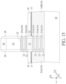
- FIG. 14 and FIG. 15 are schematic drawings illustrating a manufacturing method of the semiconductor device according to the second embodiment of the present invention, wherein FIG. 15 is a schematic drawing in a step subsequent to FIG. 14 ,
- FIG. 16 is a schematic drawing illustrating a semiconductor device according to a third embodiment of the present invention.
- FIG. 17 is a cross-sectional schematic drawing illustrating a portion of the semiconductor device according to the third embodiment of the present invention.
- FIG. 18 is a schematic drawing illustrating a layout pattern of the semiconductor device according to the third embodiment of the present invention.
- FIG. 19 is a schematic circuit diagram of the semiconductor device according to the third embodiment of the present invention.
- FIG. 20 is a schematic drawing illustrating a semiconductor device according to a fourth embodiment of the present invention.
- FIG. 21 is a schematic drawing illustrating a semiconductor device according to a fifth embodiment of the present invention.
- FIG. 22 is a schematic drawing illustrating a portion of a semiconductor device according to a sixth embodiment of the present invention.
- on not only means “directly on” something but also includes the meaning of “on” something with an intermediate feature or a layer therebetween, and that “above” or “over” not only means the meaning of “above” or “over” something but can also include the meaning it is “above” or “over” something with no intermediate feature or layer therebetween (i.e., directly on something).
- etch is used herein to describe the process of patterning a material layer so that at least a portion of the material layer after etching is retained.
- etching a material layer
- at least a portion of the material layer is retained after the end of the treatment.
- the material layer is “removed”, substantially all the material layer is removed in the process.
- “removal” is considered to be a broad term and may include etching.
- forming or the term “disposing” are used hereinafter to describe the behavior of applying a layer of material to the substrate. Such terms are intended to describe any possible layer forming techniques including, but not limited to, thermal growth, sputtering, evaporation, chemical vapor deposition, epitaxial growth, electroplating, and the like.
- FIG. 1 is a schematic drawing illustrating a semiconductor device according to a first embodiment of the present invention.
- a semiconductor device 101 includes a substrate 10 , a first transistor T 1 , a second transistor T 2 , and a first contact structure (such as a contact structure CT 1 shown in FIG. 1 ).
- the first transistor T 1 and the second transistor T 2 are disposed on the substrate 10 .
- the first transistor T 1 includes a plurality of first semiconductor channel layers 14 A, a first source/drain structure 34 A, and a second source/drain structure 34 B.
- the first semiconductor channel layers 14 A are stacked in a vertical direction (such as a first direction D 1 shown in FIG. 1 ) and separated from one another.
- the first source/drain structure 34 A and the second source/drain structure 34 B are disposed at two opposite sides of each of the first semiconductor channel layers 14 A in a horizontal direction (such as a second direction D 2 shown in FIG. 1 ), respectively.
- the first source/drain structure 34 A and the second source/drain structure 34 B are connected with the first semiconductor channel layers 14 A, respectively.
- the second transistor T 2 includes a plurality of second semiconductor channel layers 16 A, a third source/drain structure 44 A, and a fourth source/drain structure 44 B.
- the second semiconductor channel layers 16 A are disposed above the first semiconductor channel layers 14 A.
- the second semiconductor channel layers 16 A are stacked in the first direction D 1 and separated from one another.
- the third source/drain structure 44 A and the fourth source/drain structure 44 B are disposed at two opposite sides of each of the second semiconductor channel layers 16 A in the second direction D 2 , respectively.
- the third source/drain structure 44 A and the fourth source/drain structure 44 B are connected with the second semiconductor channel layers 16 A, respectively.
- the contact structure CT 1 penetrates through the third source/drain structure 44 A in the first direction D 1 .
- the first source/drain structure 34 A is electrically connected with the third source/drain structure 44 A via the contact structure CT 1 , and a part of the first source/drain structure 34 A is disposed between the substrate 10 and the contact structure CT 1 in the first direction D 1 .
- the first direction D 1 described above may be regarded as a thickness direction of the substrate 10 , and the substrate 10 may have a top surface and a bottom surface opposite to the top surface in the first direction D 1 .
- the first transistor T 1 , the second transistor T 2 , and the contact structure CT 1 may be disposed at a side of the top surface of the substrate 10 , but not limited thereto.
- horizontal directions (such as the second direction D 2 and a third direction D 3 shown in FIG. 1 ) substantially orthogonal to the first direction D 1 may be substantially parallel with the top surface and/or the bottom surface of the substrate 10 , but not limited thereto.
- a distance between the substrate 10 and a relatively higher location and/or a relatively higher part in the first direction D 1 is greater than a distance between the substrate 10 and a relatively lower location and/or a relatively lower part in the first direction D 1 .
- the bottom or a lower portion of each component may be closer to the substrate 10 in the first direction D 1 than the top or upper portion of this component.
- Another component disposed above a specific component may be regarded as being relatively far from the substrate 10 in the first direction D 1
- another component disposed under a specific component may be regarded as being relatively closer to the substrate 10 in the first direction D 1 .
- At least a part of the first transistor T 1 may be disposed between the substrate 10 and the second transistor T 2 in the first direction D 1
- at least a part of the first source/drain structure 34 A may be disposed between the substrate 10 and the third source/drain structure 44 A in the first direction D 1
- at least a part of the second source/drain structure 34 B may be disposed between the substrate 10 and the fourth source/drain structure 44 B in the first direction D 1
- at least a part of each of the first semiconductor channel layers 14 A may be disposed between the substrate 10 and the second semiconductor channel layers 16 A.
- the first transistor T 1 and the second transistor T 2 may at least partially overlap in the first direction D 1
- the first source/drain structure 34 A and the third source/drain structure 44 A may at least partially overlap in the first direction D 1
- the second source/drain structure 34 B and the fourth source/drain structure 44 B may at least partially overlap in the first direction D 1
- each of the first semiconductor channel layers 14 A and each of the second semiconductor channel layers 16 A may at least partially overlap in the first direction D 1 .
- the semiconductor device 101 may include a first gate structure GS 1 disposed on the substrate 10 , and the first gate structure GS 1 may be shared by the first transistor T 1 and the second transistor T 2 .
- the first transistor T 1 may further include a first portion GS 11 of the first gate structure GS 1
- the second transistor T 2 may further include a second portion GS 12 of the first gate structure GS 1 .
- the first portion GS 11 of the first gate structure GS 1 may encompass each of the first semiconductor channel layers 14 A
- the second portion GS 12 of the first gate structure GS 1 may encompass each of the second semiconductor channel layers 16 A.
- the first portion GS 11 of the first gate structure GS 1 may be directly connected with the second portion GS 12 of the first gate structure GS 1 , and the first portion GS 11 of the first gate structure GS 1 may be disposed between the second portion GS 12 of the first gate structure GS 1 and the substrate 10 in the first direction D 1 . Therefore, the first transistor T 1 and the second transistor T 2 may be regarded as a gate-all-around (GAA) transistor structure, respectively, but not limited thereto.
- the first gate structure GS 1 may include a gate dielectric layer 56 and a gate material layer 58 , but not limited thereto.
- the gate dielectric layer 56 may be disposed between the gate material layer 58 and each of the first semiconductor channel layers 14 A. In the second portion GS 12 of the first gate structure GS 1 , the gate dielectric layer 56 may be disposed between the gate material layer 58 and each of the second semiconductor channel layers 16 A.
- the semiconductor device 101 may further include a dielectric layer 42 disposed on the substrate 10 .
- a part of the dielectric layer 42 may be disposed between the first source/drain structure 34 A and the third source/drain structure 44 A in the first direction D 1 for separating the first source/drain structure 34 A from the third source/drain structure 44 A, and the contact structure CT 1 may further penetrate through the dielectric layer 42 in the first direction D 1 .
- another part of the dielectric layer 42 may be disposed between the second source/drain structure 34 B and the fourth source/drain structure 44 B in the first direction D 1 for separating the second source/drain structure 34 B from the fourth source/drain structure 44 B.
- the semiconductor device 101 may further include a first metal silicide layer 36 and a second metal silicide layer 46 .
- a part of the first metal silicide layer 36 may be disposed between the dielectric layer 42 and the first source/drain structure 34 A in the first direction D 1
- another part of the first metal silicide layer 36 may be disposed between the dielectric layer 42 and the second source/drain structure 34 B in the first direction D 1
- the first metal silicide layer 36 may directly contact the first source/drain structure 34 A and the second source/drain structure 34 B, but not limited thereto.
- the second metal silicide layer 46 may be disposed on and directly contact the third source/drain structure 44 A and the fourth source/drain structure 44 B, the third source/drain structure 44 A may be disposed between the second metal silicide layer 46 and the substrate 10 in the first direction D 1 , and the fourth source/drain structure 44 B may be disposed between the second metal silicide layer 46 and the substrate 10 in the first direction D 1 , but not limited thereto.
- the contact structure CT 1 may directly contact the first metal silicide layer 36 for being electrically connected with the first source/drain structure 34 A via the first metal silicide layer 36 .
- the contact structure CT 1 may not contact the first source/drain structure 34 A directly, and a part of the first metal silicide layer 36 may be disposed between the contact structure CT 1 and the first source/drain structure 34 A in the first direction D 1 , but not limited thereto.
- the damage generated by the contact structure CT 1 and/or related manufacturing processes for forming the contact structure CT 1 to the first source/drain structure 34 A and the substrate 10 may be avoided because the contact structure CT 1 does not penetrate through the first source/drain structure 34 A, and it is beneficial to the electrical performance of the first transistor T 1 and the integrated electrical performance of the semiconductor device.
- the semiconductor device 101 may further include a contact structure CT 2 , a contact structure CT 3 , and a contact structure CT 4 disposed corresponding to the second source/drain structure 34 B, the fourth source/drain structure 44 B, and the first gate structure GS 1 , respectively.
- the contact structure CT 2 may be disposed on and electrically connected with the second source/drain structure 34 B
- the contact structure CT 3 may be disposed on and electrically connected with the fourth source/drain structure 44 B
- the contact structure CT 4 may be disposed on and electrically connected with the first gate structure GS 1 .
- the contact structure CT 1 , the contact structure CT 2 , the contact structure CT 3 , and the contact structure CT 4 may be electrically separated from one another, but not limited thereto. Additionally, the fourth source/drain structure 44 B may overlap a portion of the second source/drain structure 34 B in the first direction D 1 , and the contact structure CT 2 may be disposed on another part of the second source/drain structure 34 B without overlapping the fourth source/drain structure 44 B in the first direction D 1 .
- the semiconductor device 101 may further include a spacer 28 , a spacer 32 , an etching stop layer 52 , a dielectric layer 54 , and a dielectric layer 62 .
- the spacer 32 may be disposed on sidewalls of a relatively lower portion of the first gate structure GS 1 (such as the first portion GS 11 and a part of the second portion GS 12 described above), and the spacer 28 may be disposed on sidewalls of a relatively upper portion of the first gate structure GS 1 .
- a part of the spacer 32 may be disposed between the first gate structure GS 1 and the first source/drain structure 34 A in the second direction D 2 or be disposed between the first gate structure GS 1 and the second source/drain structure 34 B in the second direction D 2 , and another part of the spacer 32 may be disposed between the first gate structure GS 1 and the third source/drain structure 44 A in the second direction D 2 or be disposed between the first gate structure GS 1 and the fourth source/drain structure 44 B in the second direction D 2 .
- the etching stop layer 52 may be disposed on sidewalls of the spacer 28 , the second metal silicide layer 46 , the third source/drain structure 44 A, the fourth source/drain structure 44 B, and the dielectric layer 42 .
- the dielectric layer 54 may be disposed on the etching stop layer 52
- the dielectric layer 62 may be disposed on the dielectric layer 54 and the first gate structure GS 1 .
- the contact structure CT 1 may penetrate through the dielectric layer 62 , the dielectric layer 54 , the etching stop layer 52 , the second metal silicide layer 46 , the third source/drain structure 44 A, and the dielectric layer 42 located above the first source/drain structure 34 A in the first direction D 1 for contacting and being electrically connected with the first metal silicide layer 36 located on the first source/drain structure 34 A;
- the contact structure CT 2 may penetrate through the dielectric layer 62 , the dielectric layer 54 , the etching stop layer 52 , and the dielectric layer 42 located above the second source/drain structure 34 B in the first direction D 1 for contacting and being electrically connected with the first metal silicide layer 36 located on the second source/drain structure 34 B;
- the contact structure CT 3 may penetrate through the dielectric layer 62 , the dielectric layer 54 , and the etching stop layer 52 located above the fourth source/drain structure 44 B in the first direction D 1 for contacting and being electrically connected with the second metal sil
- the contact structure may penetrate through the corresponding metal silicide layer and be partially disposed in the corresponding source/drain structure without penetrating through the corresponding source/drain structure.
- the contact structure CT 1 may further penetrate through the first metal silicide layer 36 and be partially disposed in the first source/drain structure 34 A without penetrating through the first source/drain structure 34 A for increasing the process window of the manufacturing process of forming the contact structure CT 1 .
- FIG. 2 is a schematic drawing illustrating a layout pattern of the semiconductor device 101 in this embodiment.
- an active region pattern P 11 and an active region pattern P 21 may be used to define locations of different active regions in the semiconductor device 101
- a gate electrode pattern P 31 may be used to define a location of the first gate structure GS 1 and/or a location of a dummy gate structure (not shown in FIG. 1 and FIG.
- a contact pattern P 41 , a contact pattern P 42 , a contact pattern P 43 , and a contact pattern P 44 may be used to define a location of the contact structure CT 1 , a location of the contact structure CT 2 , a location of the contact structure CT 3 , and a location of the contact structure CT 4 , respectively, but not limited thereto.
- the active region pattern P 11 may correspond to the location of the first semiconductor channel layer 14 A, the first source/drain structure 34 A, and the second source/drain structure 34 B in a top view of the semiconductor device
- the active region pattern P 21 may correspond to the location of the second semiconductor channel layer 16 A, the third source/drain structure 44 A, and the fourth source/drain structure 44 B in the top view of the semiconductor device.
- the area occupied by the semiconductor device 101 may be reduced by stacking the first transistor T 1 and the second transistor T 2 partially overlapping the first transistor T 1 , and it is beneficial to the density improvement of the transistors in related products.
- the first transistor T 1 may be a transistor of a first conductivity type
- the second transistor T 2 may be a transistor of a second conductivity type
- the second conductivity type may be complementary to the first conductivity type.
- the semiconductor device 101 may be regarded as an inverter, but not limited thereto.
- the first transistor T 1 may be a p-type transistor
- the second transistor T 2 may be an n-type transistor.
- the contact structure CT 1 may be electrically connected to an output terminal (such as output voltage, V output ), the contact structure CT 2 may be electrically connected to power voltage (such as V DD ), the contact structure CT 3 may be electrically connected to ground voltage (such as V GND ), and the contact structure CT 4 may be electrically connected to an input terminal (such as input voltage, V input ), but not limited thereto.
- an output terminal such as output voltage, V output
- the contact structure CT 2 may be electrically connected to power voltage (such as V DD )
- the contact structure CT 3 may be electrically connected to ground voltage (such as V GND )
- the contact structure CT 4 may be electrically connected to an input terminal (such as input voltage, V input ), but not limited thereto.
- the number of the first semiconductor channel layers 14 A in the first transistor T 1 may be different from the number of the second semiconductor channel layers 16 A in the second transistor T 2 for modifying the electrical characteristics of the first transistor T 1 and the electrical characteristics of the second transistor T 2 respectively in order to meet the design requirements, especially when the conductivity type of the first transistor T 1 is different from the conductivity type of the second transistor T 2 , but not limited thereto.
- the first transistor T 1 is a p-type transistor and the second transistor T 2 is an n-type transistor
- the number of the first semiconductor channel layers 14 A in the first transistor T 1 e.g. three first semiconductor channel layers 14 A shown in FIG. 1
- the number of the second semiconductor channel layers 16 A in the second transistor T 2 e.g. two second semiconductor channel layers 16 A shown in FIG. 1 ), but not limited thereto.
- the substrate 10 may include a semiconductor substrate, such as a silicon substrate, an epitaxial silicon substrate, a silicon germanium substrate, a silicon carbide substrate, or a silicon-on-insulator (SOI) substrate, but not limited thereto.
- the first semiconductor channel layer 14 A and the second semiconductor channel layer 16 A may include a semiconductor material, respectively, such as silicon, silicon germanium, or other suitable semiconductor materials.
- the material composition of each of the first semiconductor channel layers 14 A may be identical to or different from the material composition of each of the second semiconductor channel layers 16 A according to some design considerations.
- the first source/drain structure 34 A, the second source/drain structure 34 B, the third source/drain structure 44 A, and the fourth source/drain structure 44 B may include an epitaxial material, respectively, such as epitaxial silicon germanium (SiGe), epitaxial silicon phosphide (SiP), or other suitable epitaxial materials.
- the first metal silicide layer 36 and the second metal silicide layer 46 may include cobalt-silicide, nickel-silicide, or other suitable metal silicide materials, respectively.
- the dielectric layer 42 , the etching stop layer 52 , the dielectric layer 54 , and the dielectric layer 62 may include silicon oxide, silicon nitride, silicon oxynitride, a low dielectric constant (low-k) dielectric material, or other suitable insulation materials, respectively.
- the gate dielectric layer 56 may include a high dielectric constant (high-k) dielectric material or other suitable dielectric materials.
- the high-k dielectric material described above may include hafnium oxide (HfO 2 ), hafnium silicon oxide (HfSiO 4 ), hafnium silicon oxynitride (HfSiON), aluminum oxide (Al 2 O 3 ), tantalum oxide (Ta 2 O 5 ), zirconium oxide (ZrO 2 ), or other suitable high-k materials.
- the gate material layer 58 may include a non-metallic electrically conductive material (such as doped polysilicon) or a metallic electrically conductive material, such as a metal gate structure formed with a work function layer and a low electrical resistivity layer stacked with each other, but not limited thereto.
- the work function layer described above may include titanium nitride (TiN), titanium carbide (TiC), tantalum nitride (TaN), tantalum carbide (TaC), tungsten carbide (WC), titanium tri-aluminide (TiAl 3 ), aluminum titanium nitride (TiAlN), or other suitable electrically conductive work function materials.
- the low electrical resistivity layer described above may include tungsten, aluminum, copper, titanium aluminide, titanium, or other suitable low electrical resistivity materials.
- the contact structure CT 1 , the contact structure CT 2 , the contact structure CT 3 , and the contact structure CT 4 may include a barrier layer (not shown) and an electrically conductive material (not shown) located on the barrier layer, respectively, but not limited thereto.
- each of the contact structures may be formed of other electrically conductive structures according to some design considerations.
- the barrier layer described above may include titanium nitride, tantalum nitride, or other suitable barrier materials, and the electrically conductive material described above may include a material having relatively lower electrical resistivity, such as tungsten, aluminum, copper, titanium aluminide, and titanium, but not limited thereto.
- FIGS. 3 - 12 are schematic drawings illustrating a manufacturing method of the semiconductor device according to the first embodiment of the present invention, wherein FIG. 4 is a cross-sectional schematic drawing of FIG. 3 in another direction, FIG. 5 is a schematic drawing in a step subsequent to FIG. 3 , FIG. 6 is a schematic drawing in a step subsequent to FIG. 5 , FIG. 7 is a schematic drawing in a step subsequent to FIG. 6 , FIG. 8 is a schematic drawing in a step subsequent to FIG. 7 , FIG. 9 is a schematic drawing in a step subsequent to FIG. 8 , FIG. 10 is a schematic drawing in a step subsequent to FIG. 9 , FIG.
- a manufacturing method of the semiconductor device 101 may include the following steps.
- the first transistor T 1 and the second transistor T 2 are formed on the substrate 10 .
- the first transistor T 1 includes a plurality of the first semiconductor channel layers 14 A, the first source/drain structure 34 A, and the second source/drain structure 34 B.
- the first semiconductor channel layers 14 A are stacked in a vertical direction (such as the first direction D 1 ) and separated from one another.
- the first source/drain structure 34 A and the second source/drain structure 34 B are disposed at two opposite sides of each of the first semiconductor channel layers 14 A in a horizontal direction (such as the second direction D 2 ), respectively.
- the first source/drain structure 34 A and the second source/drain structure 34 B are connected with the first semiconductor channel layers 14 A, respectively.
- the second transistor T 2 includes a plurality of the second semiconductor channel layers 16 A, the third source/drain structure 44 A, and the fourth source/drain structure 44 B.
- the second semiconductor channel layers 16 A are disposed above the first semiconductor channel layers 14 A.
- the second semiconductor channel layers 16 A are stacked in the first direction D 1 and separated from one another.
- the third source/drain structure 44 A and the fourth source/drain structure 44 B are disposed at two opposite sides of each of the second semiconductor channel layers 16 A in the second direction D 2 , respectively.
- the third source/drain structure 44 A and the fourth source/drain structure 44 B are connected with the second semiconductor channel layers 16 A, respectively.
- the contact structure CT 1 is formed.
- the contact structure CT 1 penetrates through the third source/drain structure 44 A in the first direction D 1 .
- the first source/drain structure 34 A is electrically connected with the third source/drain structure 44 A via the contact structure CT 1 , and a part of the first source/drain structure 34 A is disposed between the substrate 10 and the contact structure CT 1 in the first direction D 1 .
- the manufacturing method of the semiconductor device 101 in this embodiment may include but is not limited to the following steps. Firstly, as shown in FIG. 3 and FIG. 4 , a stacked structure FS may be formed on the substrate 10 , and the stacked structure FS includes a plurality of first semiconductor layers 14 , a plurality of second semiconductor layers 16 , and a sacrificial material 12 .
- the first semiconductor layers 14 may be stacked in the first direction D 1
- the second semiconductor layers 16 may be disposed above the first semiconductor layers 14 and stacked in the first direction D 1 .
- the sacrificial material 12 may be partly disposed between the first semiconductor layers 14 , partly disposed between the second semiconductor layers 16 , and partly disposed between the first semiconductor layers 14 and the second semiconductor layers 16 .
- the sacrificial material 12 and the first semiconductor layers 14 may be alternately stacked in a lower portion of the stacked structure FS, and the sacrificial material 12 and the second semiconductor layers 16 may be alternately stacked in an upper portion of the stacked structure FS, but not limited thereto.
- a plurality of the stacked structures FS may be formed on the substrate 10 , each of the stacked structures FS may be substantially elongated in the second direction D 2 , and an isolation structure 18 may be disposed in the substrate 10 located between the stacked structures FS adjacent to each other, but not limited thereto.
- the isolation structure 18 may include a single layer or multiple layers of insulation materials, such as oxide insulation materials (silicon oxide and/or polysilazane, for example), or other suitable insulation materials.
- the material composition of the sacrificial material 12 may be different from the material composition of the first semiconductor layer 14 and the material composition of the second semiconductor layer 16 for providing required etching selectivity.
- the material of the first semiconductor layer 14 and the second semiconductor layer 16 may be a silicon semiconductor material
- the material of the sacrificial material 12 may be silicon germanium (SiGe) for constituting a superlattice epitaxial structure, but not limited thereto.
- SiGe silicon germanium
- other material combinations may be used to form the stacked structures FS according to some design considerations.
- the sacrificial material 12 , the first semiconductor layers 14 , and the second semiconductor layers 16 may be formed globally and stacked on the substrate 10 , and a patterning process may be performed to the sacrificial material 12 , the first semiconductor layers 14 , and the second semiconductor layers 16 for forming the stacked structures FS separated from one another, but not limited thereto.
- a dummy gate structure 20 may be formed on the stacked structure FS, and a patterning process 91 may be performed to the stacked structure FS with the dummy gate structure 20 formed thereon.
- the patterning process 91 may include an etching process or other suitable patterning approaches.
- each of the first semiconductor layers 14 may be patterned to be one of the first semiconductor channel layers 14 A by the patterning process 91
- a part of each of the second semiconductor layers 16 may be patterned to be one of the second semiconductor channel layers 16 A by the patterning process 91
- each of the first semiconductor layers 14 in the stacked structure FS may be patterned to be the first semiconductor channel layer 14 A by the patterning process 91
- each of the second semiconductor layers 16 in the stacked structure FS may be patterned to be the second semiconductor channel layer 16 A by the patterning process 91 , but not limited thereto.
- the dummy gate structure 20 may include a dielectric layer 22 , a dummy gate material 24 , and a gate cap layer 26 , and the spacer 28 may be formed on sidewalls of the dummy gate structure 20 .
- the dielectric layer 22 may include oxide or other suitable dielectric materials
- the dummy gate material 24 may include polysilicon, amorphous silicon, or other suitable materials
- the gate cap layer 26 may include nitride, oxynitride, or other suitable insulation materials, but not limited thereto.
- the patterning process 91 may be performed to the stacked structure FS with the dummy gate structure 20 and the spacer 28 as a mask, and the projection shape and/or the projection area of each of the first semiconductor channel layers 14 A in the first direction D 1 may be substantially the same as that of each of the second semiconductor channel layers 16 A in the first direction D 1 after the patterning process 91 accordingly, but not limited thereto.
- the method of forming the first semiconductor channel layers 14 A and the second semiconductor channel layers 16 A in this embodiment may include but is not limited to the steps in FIGS. 3 - 5 described above.
- the first semiconductor channel layers 14 A and the second semiconductor channel layers 16 A may be formed by other suitable approaches according to some process and/or design considerations.
- a recessing process may be performed to the sacrificial material 12 for reducing the length of the sacrificial material 12 in the second direction D 2 and further exposing a part of each of the first semiconductor channel layers 14 A and a part of each of the second semiconductor channel layers 16 A.
- the recessing process described above may include an etching process having high etching selectivity between the sacrificial material 12 , the first semiconductor channel layers 14 A, and the second semiconductor channel layers 16 A for reducing negative influence on the first semiconductor channel layers 14 A and the second semiconductor channel layers 16 A, but not limited thereto. As shown in FIG. 6 and FIG.
- the spacer 32 may then be formed on the sidewalls of the sacrificial material 12 , and an epitaxial material 34 may be formed on the substrate 10 after the step of forming the spacer 32 .
- an epitaxial growth process may be carried out from the substrate 10 , an edge of each of the first semiconductor channel layers 14 A, and/or an edge of each of the second semiconductor channel layers 16 A for forming the epitaxial material 34 , and the epitaxial material 34 may be connected with each of the first semiconductor channel layers 14 A and each of the second semiconductor channel layers 16 A accordingly, but not limited thereto. Subsequently, as shown in FIG. 7 and FIG.
- a recessing process 92 may be performed to the epitaxial material 34 for removing a part of the epitaxial material 34 in order to partially expose each of the second semiconductor channel layers 16 A and form the first source/drain structure 34 A and the second source/drain structure 34 B with the epitaxial material 34 remaining on the substrate 10 .
- at least a part of the epitaxial material 34 may be etched to be the first source/drain structure 34 A and the second source/drain structure 34 B by the recessing process 92 , but not limited thereto.
- the method of forming the first source/drain structure 34 A and the second source/drain structure 34 B in this embodiment may include but is not limited to the steps in FIGS.
- the first source/drain structure 34 A and the second source/drain structure 34 B may be formed by other suitable approaches according to some process and/or design considerations.
- the dimension of the epitaxial material 34 at the time of formation may be controlled for directly forming the first source/drain structure 34 A and the second source/drain structure 34 B without performing the recessing process 92 described above, but not limited thereto.
- the first metal silicide layer 36 may be formed on the first source/drain structure 34 A and the second source/drain structure 34 B, respectively.
- the dielectric layer 42 may be formed on the first source/drain structure 34 A and the second source/drain structure 34 B after the step of forming the first metal silicide layer 36 , a part of the first metal silicide layer 36 may be located between the first source/drain structure 34 A and the dielectric layer 42 , and another part of the first metal silicide layer 36 may be located between the second source/drain structure 34 B and the dielectric layer 42 accordingly, but not limited thereto.
- the third source/drain structure 44 A and the fourth source/drain structure 44 B are formed on the dielectric layer 42 .
- an epitaxial material 44 may be formed by performing an epitaxial growth process from the exposed edges of each of the second semiconductor channel layers 16 A, and the epitaxial material 44 may be directly connected with the second semiconductor channel layers 16 A accordingly.
- the required third source/drain structure 44 A and the required fourth source/drain structure 44 B may be formed at two opposite sides of each of the second semiconductor channel layers 16 A in the second direction D 2 by controlling the formation of the epitaxial material 44 (such as controlling the process time for forming the epitaxial material 44 ).
- a portion of the second source/drain structure 34 B may not overlap the fourth source/drain structure 44 B in the first direction D 1 by removing a part of the fourth source/drain structure 44 B, and the space for forming the contact structure corresponding to the second source/drain structure 34 B may be obtained accordingly, but not limited thereto.
- the second metal silicide layer 46 may then be formed on the third source/drain structure 44 A and the fourth source/drain structure 44 B. It is worth noting that the method of forming the third source/drain structure 44 A and the fourth source/drain structure 44 B in this embodiment may include but is not limited to the steps in FIG. 9 and FIG. 10 described above. In some embodiments, the third source/drain structure 44 A and the fourth source/drain structure 44 B may be formed by other suitable approaches according to some process and/or design considerations.
- the first gate structure GS 1 may be formed by replacing the dummy gate structure 20 and the sacrificial material 12 with the gate dielectric layer 56 and the gate material layer 58 .
- the etching stop layer 52 and the dielectric layer 54 may be formed after the step of forming the second metal silicide layer 46 , and a planarization process may be performed for removing the gate cap layer 26 , a part of the dielectric layer 54 , and a part of the etching stop layer 52 and exposing the dummy gate structure 20 .
- the planarization process described above may include a chemical mechanical polishing (CMP) process, an etching back process, or other suitable planarization approaches.
- CMP chemical mechanical polishing
- the exposed dummy gate structure 20 and the sacrificial material 12 may be removed for forming a trench TR.
- the trench TR may be surrounded by the spacer 28 and the spacer 32 in the horizontal directions, and each of the first semiconductor channel layers 14 A and each of the second semiconductor channel layers 16 A may be partly disposed in the trench TR.
- the gate dielectric layer 56 and the gate material layer 58 may be formed sequentially, and the trench TR may be filled with a part of the gate dielectric layer 56 and a part of the gate material layer 58 .
- the method of forming the first gate structure GS 1 in this embodiment may include but is not limited to the steps in FIG. 10 , FIG. 12 , and FIG. 1 described above.
- the first gate structure GS 1 may be formed by other suitable approaches according to some process and/or design considerations.
- the dielectric layer 62 , the contact structure CT 1 , the contact structure CT 2 , the contact structure CT 3 , and the contact structure CT 4 may be formed after the step of forming the first gate structure GS 1 , and the semiconductor device 101 shown in FIG. 1 may be formed accordingly.
- the first transistor T 1 and the second transistor T 2 stacked and partly overlapping may be formed, and the third source/drain structure 44 A may be electrically connected with the first source/drain structure 34 A via the contact structure CT 1 penetrating through the third source/drain structure 44 A for reducing the area occupied by the semiconductor device 101 .
- FIG. 13 is a schematic drawing illustrating a semiconductor device 102 according to a second embodiment of the present invention.
- the semiconductor device 102 may include a dielectric layer 39 and a silicon germanium layer 37 disposed on the substrate 10 .
- the dielectric layer 39 may include an oxide dielectric material or other suitable dielectric materials.
- a part of the dielectric layer 39 may be disposed between the first source/drain structure 34 A and the third source/drain structure 44 A in the first direction D 1 for separating the first source/drain structure 34 A from the third source/drain structure 44 A, and another part of the dielectric layer 39 may be disposed between the second source/drain structure 34 B and the fourth source/drain structure 44 B in the first direction D 1 for separating the second source/drain structure 34 B from the fourth source/drain structure 44 B.
- a part of the silicon germanium layer 37 may be disposed between the dielectric layer 39 and the first source/drain structure 34 A in the first direction, another part of the silicon germanium layer 37 may be disposed between the dielectric layer 39 and the second source/drain structure 34 B in the first direction D 1 , and the silicon germanium layer 37 may directly contact the first source/drain structure 34 A and the second source/drain structure 34 B, but not limited thereto.
- an atomic ratio of germanium in the silicon germanium layer 37 may be higher than an atomic ratio of germanium in the first source/drain structure 34 A and an atomic ratio of germanium in the second source/drain structure 34 B for enhancing the stress effect to the first semiconductor channel layers 14 A in the first transistor T 1 , and the silicon germanium layer 37 may be used to enhance the electrical performance of the first transistor T 1 accordingly, but not limited thereto.
- the contact structure CT 1 may penetrate through the dielectric layer 62 , the dielectric layer 54 , the etching stop layer 52 , the second metal silicide layer 46 , the third source/drain structure 44 A, the dielectric layer 39 , and the silicon germanium layer 37 located above the first source/drain structure 34 A in the first direction D 1 for contacting and being electrically connected with the first source/drain structure 34 A and the silicon germanium layer 37
- the contact structure CT 2 may penetrate through the dielectric layer 62 , the dielectric layer 54 , the etching stop layer 52 , the dielectric layer 39 , and the silicon germanium layer 37 located above the second source/drain structure 34 B in the first direction D 1 for contacting and being electrically connected with the second source/drain structure 34 B and the silicon germanium layer 37 , but not limited thereto.
- FIG. 14 and FIG. 15 are schematic drawings illustrating a manufacturing method of the semiconductor device 102 according to the second embodiment of the present invention, wherein FIG. 15 is a schematic drawing in a step subsequent to FIG. 14 , and FIG. 13 may be regarded as a schematic drawing in a step subsequent to FIG. 15 .
- the method of forming the dielectric layer 39 and the silicon germanium layer 37 may include but is not limited to the following steps. As shown in FIG. 14 and FIG. 15 , a germanium oxide layer 35 may be formed on the first source/drain structure 34 A and the second source/drain structure 34 B.
- an oxidation process 93 may be performed to the germanium oxide layer 35 , and an upper portion of the germanium oxide layer 35 may be converted into the dielectric layer 39 by the oxidation process 93 .
- the material of the first source/drain structure 34 A and the second source/drain structure 34 B includes silicon (such as epitaxial silicon germanium)
- a lower portion of the germanium oxide layer 35 and a portion of the first source/drain structure 34 A may be converted into the silicon germanium layer 37 located between the dielectric layer 39 and the first source/drain structure 34 A by the oxidation process 93
- another lower portion of the germanium oxide layer 35 and a portion of the second source/drain structure 34 B may be converted into the silicon germanium layer 37 located between the dielectric layer 39 and the second source/drain structure 34 B by the oxidation process 93 , but not limited thereto.
- the oxidation process 93 may be regarded as a condensation annealing process configured to make the silicon in the first source/drain structure 34 A and the second source/drain structure 34 B diffuse upwards for forming the dielectric layer 39 composed of silicon oxide and make the germanium in the germanium oxide layer 35 diffuse downwards for forming the silicon germanium layer 37 with relatively higher germanium concentration, but not limited thereto.
- the remaining germanium oxide layer 35 (such as the germanium oxide layer 35 formed on the gate cap layer 26 , the spacer 28 , the sidewall of the spacer 32 , and the sidewall of the second semiconductor channel layer 16 A) may be removed for avoiding the influence of the germanium oxide layer 35 on the subsequent process of forming the third source/drain structure 44 A and the fourth source/drain structure 44 B (as shown in FIG. 13 ).
- FIG. 16 is a schematic drawing illustrating a semiconductor device 103 according to a third embodiment of the present invention.
- the semiconductor device 103 may further include a plurality of third semiconductor channel layers 16 B and a fifth source/drain structure 44 C.
- the third semiconductor channel layers 16 B and the fifth source/drain structure 44 C are disposed on the substrate 10 .
- the third semiconductor channel layers 16 B may be stacked in the first direction D 1
- the third source/drain structure 44 A may be disposed between one of the second semiconductor channel layers 16 A and one of the third semiconductor channel layers 16 B in the second direction D 2 .
- the third semiconductor channel layers 16 B may be disposed between the fifth source/drain structure 44 C and the third source/drain structure 44 A in the second direction D 2 , and the third semiconductor channel layers 16 B, the fifth source/drain structure 44 C, and the third source/drain structure 44 A may constitute a portion of a third transistor T 3 .
- the third source/drain structure 44 A may be shared by the second transistor T 2 and the third transistor T 3 for reducing the area occupied by the semiconductor device 103 , but not limited thereto.
- the semiconductor device 103 may further include a second gate structure GS 2 , a contact structure CT 5 , and a contact structure CT 6 .
- the second gate structure GS 2 and the first gate structure GS 1 may be formed concurrently by the same manufacturing process, and the second gate structure GS 2 may include the gate dielectric layer 56 and the gate material layer 58 also.
- the second gate structure GS 2 may encompass each of the third semiconductor channel layers 16 B, and the spacer 28 and the spacer 32 may further disposed on sidewalls of the second gate structure GS 2 , respectively, but not limited thereto.
- a part of the second metal silicide layer 46 may be formed on the fifth source/drain structure 44 C, the contact structure CT 6 may penetrate through the dielectric layer 62 located above the second gate structure GS 2 in the first direction D 1 for contacting and being electrically connected with the second gate structure GS 2 , and the contact structure CT 5 may penetrate through the dielectric layer 62 , the dielectric layer 54 , and the etching stop layer 52 located above the fifth source/drain structure 44 C in the first direction D 1 for contacting the second metal silicide layer 46 and being electrically connected with the fifth source/drain structure 44 C via the second metal silicide layer 46 , but not limited thereto.
- the contact structure CT 5 , the contact structure CT 6 , the contact structure CT 1 , the contact structure CT 2 , the contact structure CT 3 , and the contact structure CT 4 described above may be formed concurrently by the same manufacturing process and have the same material composition, but not limited thereto.
- FIG. 17 is a cross-sectional schematic drawing illustrating a portion of the semiconductor device in this embodiment
- FIG. 18 is a schematic drawing illustrating a layout pattern of the semiconductor device in this embodiment
- FIG. 19 is a schematic circuit diagram of the semiconductor device in this embodiment.
- the first transistor T 1 may be a pull-up transistor in a static random access memory (SRAM) structure, which is a p-type transistor
- the second transistor T 2 may be a pull-down transistor in this SRAM structure, which is an n-type transistor
- the third transistor T 3 may be a passing gate transistor in this SRAM structure, which is an n-type, but not limited thereto.
- SRAM static random access memory
- the semiconductor device in this embodiment may further include a fourth transistor T 4 , a fifth transistor T 5 , and a sixth transistor T 6 .
- the fourth transistor T 4 may be another pull-up transistor in this SRAM structure, which is a p-type transistor; the fifth transistor T 5 may be another pull-down transistor in this SRAM structure, which is an n-type transistor; and the sixth transistor T 6 may be another passing gate transistor in this SRAM structure, which is an n-type, but not limited thereto.
- a source electrode SE 1 of the first transistor T 1 (such as the second source/drain structure 34 B) may be electrically connected to a voltage source VS 1
- a drain electrode DE 1 of the first transistor T 1 (such as the first source/drain structure 34 A) may be electrically connected with a drain electrode DE 2 of the second transistor T 2 (such as the third source/drain structure 44 A).
- a gate electrode GE 1 of the first transistor T 1 (such as the first portion GS 11 of the first gate structure GS 1 ) may be electrically connected with a gate electrode GE 2 of the second transistor T 2 (such as the second portion GS 12 of the first gate structure GS 1 ), and a source electrode SE 2 of the second transistor T 2 (such as the fourth source/drain structure 44 B) may be electrically connected to a voltage source VS 2 .
- a drain electrode DE 3 of the third transistor T 3 (such as the third source/drain structure 44 A) may be electrically connected with the drain electrode DE 1 of the first transistor T 1 and the drain electrode DE 2 of the second transistor T 2 , and a gate electrode GE 3 of the third transistor T 3 (such as a first portion GS 21 of the second gate structure GS 2 ) and a source electrode SE 3 of the third transistor T 3 (such as the fifth source/drain structure 44 C) may be electrically connected to a word line WL and a bit line BL, respectively.
- a source electrode SE 4 of the fourth transistor T 4 may be electrically connected to the voltage source VS 1
- a drain electrode DE 4 of the fourth transistor T 4 may be electrically connected with a drain electrode DE 5 of the fifth transistor T 5
- a gate electrode GE 4 of the fourth transistor T 4 may be electrically connected with a gate electrode GE 5 of the fifth transistor T 5
- a source electrode SE 5 of the fifth transistor T 5 may be electrically connected to the voltage source VS 2 .
- a drain electrode DE 6 of the sixth transistor T 6 may be electrically connected with the drain electrode DE 4 of the fourth transistor T 4 and the drain electrode DE 5 of the fifth transistor T 5
- a gate electrode GE 6 and a source electrode SE 6 of the sixth transistor T 6 may be electrically connected to the word line WL and another bit line BLB, respectively.
- the voltage source VS 1 may be power voltage (such as V DD )
- the voltage source VS 2 may be ground voltage (such as V GND )
- the static random access memory structure in this embodiment may be regarded as a six-transistor SRAM ( 6 T-SRAM), but not limited thereto.
- the fourth transistor T 4 , the fifth transistor T 5 , and the sixth transistor T 6 may be disposed substantially symmetrical to the first transistor T 1 , the second transistor T 2 , and the third transistor T 3 , respectively.
- the cross-section structure of the fourth transistor T 4 may be similar to the cross-section structure of the first transistor T 1 shown in FIG. 16
- the cross-section structure of the fifth transistor T 5 may be similar to the cross-section structure of the second transistor T 2 shown in FIG. 16
- the cross-section structure of the sixth transistor T 6 may be similar to the cross-section structure of the third transistor T 3 shown in FIG. 16 , but not limited thereto. As shown in FIG. 16 and FIG.
- the active region pattern P 11 , an active region pattern P 12 , the active region pattern P 21 , an active region pattern P 22 , an active region pattern P 23 , and an active region pattern P 24 may be used to define locations of different active regions in the semiconductor device of this embodiment.
- the active region pattern P 11 may correspond to the location of the first semiconductor channel layer 14 A, the first source/drain structure 34 A, and the second source/drain structure 34 B of the first transistor T 1 in a top view of the semiconductor device;
- the active region pattern P 12 may correspond to the location of a semiconductor channel layer (not shown) and source/drain structures (such as the source electrode SE 4 and the drain electrode DE 4 ) of the fourth transistor T 4 in the top view of the semiconductor device;
- the active region pattern P 21 may correspond to the location of the second semiconductor channel layer 16 A, the third source/drain structure 44 A, and the fourth source/drain structure 44 B of the second transistor T 2 in the top view of the semiconductor device;
- the active region pattern P 22 may correspond to the location of the third semiconductor channel layer 16 B, the third source/drain structure 44 A, and the fifth source/drain structure 44 C of the third transistor T 3 in the top view of the semiconductor device;
- the active region pattern P 23 may correspond to the location of a semiconductor channel layer (not shown) and
- the gate electrode pattern P 31 may be used to define the location of the first gate structure GS 1 and/or the location of the dummy gate structure corresponding to the first gate structure GS 1 (such as the dummy gate structure 20 shown in FIG. 10 ); a gate electrode pattern P 32 may be used to define the location of the second gate structure GS 2 and/or the location of the dummy gate structure corresponding to the second gate structure GS 2 (not shown); a gate electrode pattern P 33 may be used to define the location of the gate structure of the fourth transistor T 4 and the fifth transistor T 5 (such as the gate electrode GE 4 and the gate electrode GE 5 ) and/or the location of the dummy gate structure corresponding to this gate structure (not shown); and a gate electrode pattern P 34 may be used to define the location of the gate structure of the sixth transistor T 6 (such as the gate electrode GE 6 ) and/or the location of the dummy gate structure corresponding to this gate structure (not shown).
- the contact pattern P 41 , the contact pattern P 42 , the contact pattern P 43 , the contact pattern P 44 , a contact pattern P 45 , and a contact pattern P 46 may be used to define the location of the contact structure CT 1 , the location of the contact structure CT 2 , the location of the contact structure CT 3 , the location of the contact structure CT 4 , the location of the contact structure CT 5 , and the location of the contact structure CT 6 , respectively.
- a contact pattern P 51 , a contact pattern P 52 , a contact pattern P 53 , a contact pattern P 54 , a contact pattern P 55 , and a contact pattern P 56 may be used to define a location of a contact structure corresponding to the drain electrode DE 4 of the fourth transistor T 4 and the drain electrode DE 5 of the fifth transistor T 5 (not shown), a location of a contact structure corresponding to the source electrode SE 4 of the fourth transistor T 4 (not shown), a location of a contact structure corresponding to the source electrode SE 5 of the fifth transistor T 5 (not shown), a location of a contact structure corresponding to a gate structure shared by the fourth transistor T 4 and the fifth transistor T 5 (not shown), a location of a contact structure corresponding to the source electrode SE 6 of the sixth transistor T 6 (not shown), and a location of a contact structure corresponding to the gate electrode GE 6 of the sixth transistor T 6 (not shown), respectively.
- connection pattern P 61 may be used to define a location of a connection structure electrically connecting the drain electrode DE 1 of the first transistor T 1 and the gate electrode GE 4 of the fourth transistor T 4 (not shown), and a connection pattern P 62 may be used to define a location of a connection structure electrically connecting the drain electrode DE 4 of the fourth transistor T 4 and the gate electrode GE 1 of the first transistor T 1 (not shown), but not limited thereto.
- the area occupied by the structure of the SRAM memory unit may be reduced by stacking the first transistor T 1 and the second transistor T 2 partially overlapping the first transistor T 1 and stacking the fourth transistor T 4 and the fifth transistor T 5 partially overlapping the fourth transistor T 4 , and it is beneficial to the density improvement of the memory units in related products.
- a width W 1 of each of the first semiconductor channel layers 14 A may be substantially equal to a width W 2 of each of the second semiconductor channel layers 16 A, but not limited thereto.
- the width W 1 of each of the first semiconductor channel layers 14 A may be regarded as a length of each of the first semiconductor channel layers 14 A in the third direction D 3
- the width W 2 of each of the second semiconductor channel layers 16 A may be regarded as a length of each of the second semiconductor channel layers 16 A in the third direction D 3
- the third direction D 3 may be substantially orthogonal to the second direction D 2 , but not limited thereto.
- a cross-sectional shape of the epitaxial material 34 may be different from a cross-sectional shape of the epitaxial material 44 because the material compositions of the epitaxial materials are different from each other, but not limited thereto.
- FIG. 20 is a schematic drawing illustrating a semiconductor device 104 according to a fourth embodiment of the present invention.
- a thickness TK 1 of each of the first semiconductor channel layers 14 A in the first direction D 1 may be different from a thickness TK 2 of each of the second semiconductor channel layers 16 A in the first direction D 1 for adjusting the surface area of the first semiconductor channel layers 14 A encompassed by the first gate structure GS 1 in the first transistor T 1 and the surface area of the second semiconductor channel layers 16 A encompassed by the first gate structure GS 1 in the second transistor T 2 , respectively, and the electrical characteristics of the first transistor T 1 and the second transistor T 2 may meet the design requirements accordingly, especially when the conductivity type of the first transistor T 1 is different from the conductivity type of the second transistor T 2 , but not limited thereto.
- the thickness TK 1 of each of the first semiconductor channel layers 14 A may be greater than the thickness TK 2 of each of the second semiconductor channel layers 16 A, and the number of the first semiconductor channel layers 14 A in the first transistor T 1 may be equal to the number of the second semiconductor channel layers 16 A in the second transistor T 2 , but not limited thereto.
- the thickness TK 1 of each of the first semiconductor channel layers 14 A may be different from the thickness TK 2 of each of the second semiconductor channel layers 16 A while the number of the first semiconductor channel layers 14 A in the first transistor T 1 is different from the number of the second semiconductor channel layers 16 A in the second transistor T 2 according to some design considerations.
- FIG. 21 is a schematic drawing illustrating a semiconductor device 105 according to a fifth embodiment of the present invention.
- the number of the first semiconductor channel layers 14 A in the first transistor T 1 may be equal to the number of the second semiconductor channel layers 16 A in the second transistor T 2
- the thickness of each of the first semiconductor channel layers 14 A may be substantially equal to the thickness of each of the second semiconductor channel layers 16 A
- the material composition of each of the first semiconductor channel layers 14 A may be different from the material composition of each of the second semiconductor channel layers 16 A for modifying the electrical characteristics of the first transistor T 1 and the electrical characteristics of the second transistor T 2 respectively in order to meet the design requirements, especially when the conductivity type of the first transistor T 1 is different from the conductivity type of the second transistor T 2 , but not limited thereto.
- FIG. 22 is a schematic drawing illustrating a portion of a semiconductor device 106 according to a sixth embodiment of the present invention.
- the width W 1 of each of the first semiconductor channel layers 14 A may be different from the width W 2 of each of the second semiconductor channel layers 16 A for modifying the electrical characteristics of the first transistor T 1 and the electrical characteristics of the second transistor T 2 respectively in order to meet the design requirements, especially when the conductivity type of the first transistor T 1 is different from the conductivity type of the second transistor T 2 , but not limited thereto.
- the width W 1 of each of the first semiconductor channel layers 14 A may be greater than the width W 2 of each of the second semiconductor channel layers 16 A, and the surface area of the first semiconductor channel layers 14 A encompassed by the first gate structure GS 1 in the first transistor T 1 may be greater than the surface area of the second semiconductor channel layers 16 A encompassed by the first gate structure GS 1 in the second transistor T 2 accordingly.
- the width W 1 of each of the first semiconductor channel layers 14 A is different from the width W 2 of each of the second semiconductor channel layers 16 A
- the number of the first semiconductor channel layers 14 A in the first transistor T 1 may be equal to or different from the number of the second semiconductor channel layers 16 A in the second transistor T 2 according to some process and/or design considerations.
- two transistors are stacked and partially overlap, and the source/drain structures of the stacked transistors are electrically connected with each other via the contact structure penetrating through the source/drain structure of the upper transistor.
- the area occupied by the semiconductor device may be reduced, and the density of the transistors and/or the density of the semiconductor units (such as the memory units) in the related product may be increased accordingly.
Landscapes
- Thin Film Transistor (AREA)
- Metal-Oxide And Bipolar Metal-Oxide Semiconductor Integrated Circuits (AREA)
Abstract
Description
Claims (13)
Applications Claiming Priority (2)
| Application Number | Priority Date | Filing Date | Title |
|---|---|---|---|
| CN202011013769.9 | 2020-09-24 | ||
| CN202011013769.9A CN114256231A (en) | 2020-09-24 | 2020-09-24 | Semiconductor device and method for manufacturing the same |
Publications (2)
| Publication Number | Publication Date |
|---|---|
| US20220093593A1 US20220093593A1 (en) | 2022-03-24 |
| US11894373B2 true US11894373B2 (en) | 2024-02-06 |
Family
ID=80740876
Family Applications (1)
| Application Number | Title | Priority Date | Filing Date |
|---|---|---|---|
| US17/083,342 Active 2041-04-09 US11894373B2 (en) | 2020-09-24 | 2020-10-29 | Semiconductor device and manufacturing method thereof |
Country Status (2)
| Country | Link |
|---|---|
| US (1) | US11894373B2 (en) |
| CN (1) | CN114256231A (en) |
Cited By (1)
| Publication number | Priority date | Publication date | Assignee | Title |
|---|---|---|---|---|
| US20230420458A1 (en) * | 2022-06-23 | 2023-12-28 | International Business Machines Corporation | Dummy fin contact in vertically stacked transistors |
Families Citing this family (12)
| Publication number | Priority date | Publication date | Assignee | Title |
|---|---|---|---|---|
| WO2022088056A1 (en) * | 2020-10-30 | 2022-05-05 | 华为技术有限公司 | Method for forming sidewall in fork-shaped structure and semiconductor device with fork-shaped structure |
| US11968818B2 (en) * | 2021-03-19 | 2024-04-23 | Samsung Electronics Co., Ltd. | SRAM memory cell for stacked transistors with different channel width |
| KR102877120B1 (en) * | 2021-08-13 | 2025-10-27 | 삼성전자주식회사 | Semiconductor device |
| US12278184B2 (en) * | 2022-03-31 | 2025-04-15 | International Business Machines Corporation | Vertically-stacked field effect transistor cell |
| US12419077B2 (en) * | 2022-06-23 | 2025-09-16 | Taiwan Semiconductor Manufacturing Company, Ltd. | Method for forming dual silicide in manufacturing process of semiconductor structure |
| EP4300559A1 (en) * | 2022-06-27 | 2024-01-03 | Imec VZW | A method for forming a semiconductor device |
| US20240006413A1 (en) * | 2022-07-01 | 2024-01-04 | Intel Corporation | Independent gate stack for single nanowire standard cell transistors |
| US12342571B2 (en) * | 2022-07-11 | 2025-06-24 | Nanya Technology Corporation | Method for manufacturing semiconductor device with passing gate |
| EP4391038A1 (en) * | 2022-12-20 | 2024-06-26 | Imec VZW | A method for forming a semiconductor device |
| US12446264B2 (en) * | 2022-12-20 | 2025-10-14 | Qualcomm Incorporated | Complementary field effect transistor (CFET) with balanced N and P drive current |
| EP4460162A1 (en) * | 2023-05-04 | 2024-11-06 | Imec VZW | A high performance and low power 3d sram cell and process integration flow |
| US12131954B1 (en) * | 2023-12-06 | 2024-10-29 | Taiwan Semiconductor Manufacturing Co., Ltd. | Selective epitaxy process for the formation of CFET local interconnection |
Citations (12)
| Publication number | Priority date | Publication date | Assignee | Title |
|---|---|---|---|---|
| US8466451B2 (en) | 2009-05-21 | 2013-06-18 | International Business Machines Corporation | Single gate inverter nanowire mesh |
| US20170040321A1 (en) * | 2015-08-06 | 2017-02-09 | Imec Vzw | Gate-all-around nanowire device and method for manufacturing such a device |
| US10164121B2 (en) | 2015-11-25 | 2018-12-25 | Samsung Electronics Co., Ltd. | Stacked independently contacted field effect transistor having electrically separated first and second gates |
| US20190131184A1 (en) * | 2017-11-02 | 2019-05-02 | International Business Machines Corporation | Stacked field-effect transistors (fets) with shared and non-shared gates |
| US20190131395A1 (en) * | 2017-11-02 | 2019-05-02 | International Business Machines Corporation | Vertically stacked dual channel nanosheet devices |
| US10304833B1 (en) * | 2018-02-19 | 2019-05-28 | Globalfoundries Inc. | Method of forming complementary nano-sheet/wire transistor devices with same depth contacts |
| US20190319095A1 (en) * | 2017-11-02 | 2019-10-17 | International Business Machines Corporation | Vertically stacked nfets and pfets with gate-all-around structure |
| US20190326286A1 (en) * | 2018-04-20 | 2019-10-24 | Globalfoundries Inc. | Method, apparatus, and system for fin-over-nanosheet complementary field-effect-transistor |
| US20200098756A1 (en) | 2018-09-21 | 2020-03-26 | Intel Corporation | Stacked nanowire transistor structure with different channel geometries for stress |
| US20200118891A1 (en) | 2018-10-10 | 2020-04-16 | International Business Machines Corporation | Vertically stacked nanosheet cmos transistor |
| US20200203343A1 (en) * | 2016-09-30 | 2020-06-25 | Institute of Microelectronics, Chinese Academy of Sciences | Ic unit and method of manufacturing the same, and electronic device including the same |
| US20220037497A1 (en) * | 2020-07-31 | 2022-02-03 | Taiwan Semiconductor Manufacturing Co., Ltd. | Stacked Multi-Gate Structure And Methods Of Fabricating The Same |
Family Cites Families (3)
| Publication number | Priority date | Publication date | Assignee | Title |
|---|---|---|---|---|
| CN104733389B (en) * | 2013-12-20 | 2018-11-16 | 中芯国际集成电路制造(上海)有限公司 | The forming method of transistor |
| US9837414B1 (en) * | 2016-10-31 | 2017-12-05 | International Business Machines Corporation | Stacked complementary FETs featuring vertically stacked horizontal nanowires |
| CN109148299B (en) * | 2017-06-28 | 2022-03-11 | 中芯国际集成电路制造(上海)有限公司 | Semiconductor device and method of manufacturing the same |
-
2020
- 2020-09-24 CN CN202011013769.9A patent/CN114256231A/en active Pending
- 2020-10-29 US US17/083,342 patent/US11894373B2/en active Active
Patent Citations (12)
| Publication number | Priority date | Publication date | Assignee | Title |
|---|---|---|---|---|
| US8466451B2 (en) | 2009-05-21 | 2013-06-18 | International Business Machines Corporation | Single gate inverter nanowire mesh |
| US20170040321A1 (en) * | 2015-08-06 | 2017-02-09 | Imec Vzw | Gate-all-around nanowire device and method for manufacturing such a device |
| US10164121B2 (en) | 2015-11-25 | 2018-12-25 | Samsung Electronics Co., Ltd. | Stacked independently contacted field effect transistor having electrically separated first and second gates |
| US20200203343A1 (en) * | 2016-09-30 | 2020-06-25 | Institute of Microelectronics, Chinese Academy of Sciences | Ic unit and method of manufacturing the same, and electronic device including the same |
| US20190131184A1 (en) * | 2017-11-02 | 2019-05-02 | International Business Machines Corporation | Stacked field-effect transistors (fets) with shared and non-shared gates |
| US20190131395A1 (en) * | 2017-11-02 | 2019-05-02 | International Business Machines Corporation | Vertically stacked dual channel nanosheet devices |
| US20190319095A1 (en) * | 2017-11-02 | 2019-10-17 | International Business Machines Corporation | Vertically stacked nfets and pfets with gate-all-around structure |
| US10304833B1 (en) * | 2018-02-19 | 2019-05-28 | Globalfoundries Inc. | Method of forming complementary nano-sheet/wire transistor devices with same depth contacts |
| US20190326286A1 (en) * | 2018-04-20 | 2019-10-24 | Globalfoundries Inc. | Method, apparatus, and system for fin-over-nanosheet complementary field-effect-transistor |
| US20200098756A1 (en) | 2018-09-21 | 2020-03-26 | Intel Corporation | Stacked nanowire transistor structure with different channel geometries for stress |
| US20200118891A1 (en) | 2018-10-10 | 2020-04-16 | International Business Machines Corporation | Vertically stacked nanosheet cmos transistor |
| US20220037497A1 (en) * | 2020-07-31 | 2022-02-03 | Taiwan Semiconductor Manufacturing Co., Ltd. | Stacked Multi-Gate Structure And Methods Of Fabricating The Same |
Cited By (2)
| Publication number | Priority date | Publication date | Assignee | Title |
|---|---|---|---|---|
| US20230420458A1 (en) * | 2022-06-23 | 2023-12-28 | International Business Machines Corporation | Dummy fin contact in vertically stacked transistors |
| US12364004B2 (en) * | 2022-06-23 | 2025-07-15 | International Business Machines Corporation | Dummy fin contact in vertically stacked transistors |
Also Published As
| Publication number | Publication date |
|---|---|
| CN114256231A (en) | 2022-03-29 |
| US20220093593A1 (en) | 2022-03-24 |
Similar Documents
| Publication | Publication Date | Title |
|---|---|---|
| US11894373B2 (en) | Semiconductor device and manufacturing method thereof | |
| US8035170B2 (en) | Semiconductor device including SRAM | |
| US10340272B2 (en) | Manufacturing method of semiconductor device | |
| US11721697B2 (en) | Manufacturing method of semiconductor device | |
| US10141312B2 (en) | Semiconductor devices including insulating materials in fins | |
| US12255245B2 (en) | Manufacturing method of semiconductor device | |
| US8361854B2 (en) | Fin field-effect transistor structure and manufacturing process thereof | |
| US10211212B2 (en) | Semiconductor devices | |
| US10833169B1 (en) | Metal gate for a field effect transistor and method | |
| US9673106B2 (en) | Semiconductor devices and methods of manufacturing the same | |
| KR20210097611A (en) | Isolation structures for semiconductor devices | |
| US11476348B2 (en) | Semiconductor device | |
| US9755048B2 (en) | Patterned structure of a semiconductor device and a manufacturing method thereof | |
| CN110610855B (en) | Method for manufacturing semiconductor device | |
| US12087666B2 (en) | Semiconductor device | |
| US20230215913A1 (en) | Manufacturing method of semiconductor device | |
| US10651174B2 (en) | FinFET structure and fabricating method of gate structure | |
| US20240339495A1 (en) | Semiconductor device and manufacturing method thereof | |
| US20250107150A1 (en) | Semiconductor devices | |
| US20250040215A1 (en) | Semiconductor device and method for fabricating the same | |
| US20230276619A1 (en) | Semiconductor devices having cell array and peripheral regions therein | |
| KR20250052971A (en) | Semiconductor structure and method for forming the same | |
| CN117995777A (en) | Semiconductor element and method for manufacturing the same |
Legal Events
| Date | Code | Title | Description |
|---|---|---|---|
| AS | Assignment |
Owner name: UNITED MICROELECTRONICS CORP., TAIWAN Free format text: ASSIGNMENT OF ASSIGNORS INTEREST;ASSIGNOR:YANG, PO-YU;REEL/FRAME:054202/0739 Effective date: 20201026 |
|
| FEPP | Fee payment procedure |
Free format text: ENTITY STATUS SET TO UNDISCOUNTED (ORIGINAL EVENT CODE: BIG.); ENTITY STATUS OF PATENT OWNER: LARGE ENTITY |
|
| STPP | Information on status: patent application and granting procedure in general |
Free format text: DOCKETED NEW CASE - READY FOR EXAMINATION |
|
| STPP | Information on status: patent application and granting procedure in general |
Free format text: NON FINAL ACTION MAILED |
|
| STPP | Information on status: patent application and granting procedure in general |
Free format text: RESPONSE TO NON-FINAL OFFICE ACTION ENTERED AND FORWARDED TO EXAMINER |
|
| STPP | Information on status: patent application and granting procedure in general |
Free format text: NON FINAL ACTION MAILED |
|
| STPP | Information on status: patent application and granting procedure in general |
Free format text: RESPONSE AFTER FINAL ACTION FORWARDED TO EXAMINER |
|
| STPP | Information on status: patent application and granting procedure in general |
Free format text: FINAL REJECTION MAILED |
|
| STPP | Information on status: patent application and granting procedure in general |
Free format text: DOCKETED NEW CASE - READY FOR EXAMINATION |
|
| STPP | Information on status: patent application and granting procedure in general |
Free format text: NOTICE OF ALLOWANCE MAILED -- APPLICATION RECEIVED IN OFFICE OF PUBLICATIONS |
|
| STPP | Information on status: patent application and granting procedure in general |
Free format text: PUBLICATIONS -- ISSUE FEE PAYMENT VERIFIED |
|
| STCF | Information on status: patent grant |
Free format text: PATENTED CASE |