US11873214B2 - Nano-electro-mechanical tags for identification and authentication - Google Patents
Nano-electro-mechanical tags for identification and authentication Download PDFInfo
- Publication number
- US11873214B2 US11873214B2 US17/152,294 US202117152294A US11873214B2 US 11873214 B2 US11873214 B2 US 11873214B2 US 202117152294 A US202117152294 A US 202117152294A US 11873214 B2 US11873214 B2 US 11873214B2
- Authority
- US
- United States
- Prior art keywords
- nems
- layer
- conductive layer
- tag
- spectral signature
- Prior art date
- Legal status (The legal status is an assumption and is not a legal conclusion. Google has not performed a legal analysis and makes no representation as to the accuracy of the status listed.)
- Active, expires
Links
Images


Classifications
-
- B—PERFORMING OPERATIONS; TRANSPORTING
- B81—MICROSTRUCTURAL TECHNOLOGY
- B81C—PROCESSES OR APPARATUS SPECIALLY ADAPTED FOR THE MANUFACTURE OR TREATMENT OF MICROSTRUCTURAL DEVICES OR SYSTEMS
- B81C1/00—Manufacture or treatment of devices or systems in or on a substrate
- B81C1/00015—Manufacture or treatment of devices or systems in or on a substrate for manufacturing microsystems
- B81C1/00134—Manufacture or treatment of devices or systems in or on a substrate for manufacturing microsystems comprising flexible or deformable structures
- B81C1/0019—Flexible or deformable structures not provided for in groups B81C1/00142 - B81C1/00182
-
- B—PERFORMING OPERATIONS; TRANSPORTING
- B81—MICROSTRUCTURAL TECHNOLOGY
- B81C—PROCESSES OR APPARATUS SPECIALLY ADAPTED FOR THE MANUFACTURE OR TREATMENT OF MICROSTRUCTURAL DEVICES OR SYSTEMS
- B81C1/00—Manufacture or treatment of devices or systems in or on a substrate
- B81C1/00015—Manufacture or treatment of devices or systems in or on a substrate for manufacturing microsystems
- B81C1/00134—Manufacture or treatment of devices or systems in or on a substrate for manufacturing microsystems comprising flexible or deformable structures
- B81C1/00142—Bridges
-
- H—ELECTRICITY
- H10—SEMICONDUCTOR DEVICES; ELECTRIC SOLID-STATE DEVICES NOT OTHERWISE PROVIDED FOR
- H10N—ELECTRIC SOLID-STATE DEVICES NOT OTHERWISE PROVIDED FOR
- H10N30/00—Piezoelectric or electrostrictive devices
- H10N30/01—Manufacture or treatment
- H10N30/05—Manufacture of multilayered piezoelectric or electrostrictive devices, or parts thereof, e.g. by stacking piezoelectric bodies and electrodes
-
- H—ELECTRICITY
- H10—SEMICONDUCTOR DEVICES; ELECTRIC SOLID-STATE DEVICES NOT OTHERWISE PROVIDED FOR
- H10N—ELECTRIC SOLID-STATE DEVICES NOT OTHERWISE PROVIDED FOR
- H10N30/00—Piezoelectric or electrostrictive devices
- H10N30/01—Manufacture or treatment
- H10N30/06—Forming electrodes or interconnections, e.g. leads or terminals
-
- H—ELECTRICITY
- H10—SEMICONDUCTOR DEVICES; ELECTRIC SOLID-STATE DEVICES NOT OTHERWISE PROVIDED FOR
- H10N—ELECTRIC SOLID-STATE DEVICES NOT OTHERWISE PROVIDED FOR
- H10N30/00—Piezoelectric or electrostrictive devices
- H10N30/01—Manufacture or treatment
- H10N30/07—Forming of piezoelectric or electrostrictive parts or bodies on an electrical element or another base
- H10N30/074—Forming of piezoelectric or electrostrictive parts or bodies on an electrical element or another base by depositing piezoelectric or electrostrictive layers, e.g. aerosol or screen printing
- H10N30/076—Forming of piezoelectric or electrostrictive parts or bodies on an electrical element or another base by depositing piezoelectric or electrostrictive layers, e.g. aerosol or screen printing by vapour phase deposition
-
- H—ELECTRICITY
- H10—SEMICONDUCTOR DEVICES; ELECTRIC SOLID-STATE DEVICES NOT OTHERWISE PROVIDED FOR
- H10N—ELECTRIC SOLID-STATE DEVICES NOT OTHERWISE PROVIDED FOR
- H10N30/00—Piezoelectric or electrostrictive devices
- H10N30/01—Manufacture or treatment
- H10N30/08—Shaping or machining of piezoelectric or electrostrictive bodies
- H10N30/081—Shaping or machining of piezoelectric or electrostrictive bodies by coating or depositing using masks, e.g. lift-off
-
- H—ELECTRICITY
- H10—SEMICONDUCTOR DEVICES; ELECTRIC SOLID-STATE DEVICES NOT OTHERWISE PROVIDED FOR
- H10N—ELECTRIC SOLID-STATE DEVICES NOT OTHERWISE PROVIDED FOR
- H10N30/00—Piezoelectric or electrostrictive devices
- H10N30/01—Manufacture or treatment
- H10N30/09—Forming piezoelectric or electrostrictive materials
- H10N30/093—Forming inorganic materials
-
- H—ELECTRICITY
- H10—SEMICONDUCTOR DEVICES; ELECTRIC SOLID-STATE DEVICES NOT OTHERWISE PROVIDED FOR
- H10N—ELECTRIC SOLID-STATE DEVICES NOT OTHERWISE PROVIDED FOR
- H10N30/00—Piezoelectric or electrostrictive devices
- H10N30/50—Piezoelectric or electrostrictive devices having a stacked or multilayer structure
-
- H—ELECTRICITY
- H10—SEMICONDUCTOR DEVICES; ELECTRIC SOLID-STATE DEVICES NOT OTHERWISE PROVIDED FOR
- H10N—ELECTRIC SOLID-STATE DEVICES NOT OTHERWISE PROVIDED FOR
- H10N30/00—Piezoelectric or electrostrictive devices
- H10N30/80—Constructional details
- H10N30/85—Piezoelectric or electrostrictive active materials
-
- H—ELECTRICITY
- H10—SEMICONDUCTOR DEVICES; ELECTRIC SOLID-STATE DEVICES NOT OTHERWISE PROVIDED FOR
- H10N—ELECTRIC SOLID-STATE DEVICES NOT OTHERWISE PROVIDED FOR
- H10N30/00—Piezoelectric or electrostrictive devices
- H10N30/80—Constructional details
- H10N30/87—Electrodes or interconnections, e.g. leads or terminals
-
- B—PERFORMING OPERATIONS; TRANSPORTING
- B81—MICROSTRUCTURAL TECHNOLOGY
- B81B—MICROSTRUCTURAL DEVICES OR SYSTEMS, e.g. MICROMECHANICAL DEVICES
- B81B2201/00—Specific applications of microelectromechanical systems
- B81B2201/02—Sensors
- B81B2201/0271—Resonators; ultrasonic resonators
-
- B—PERFORMING OPERATIONS; TRANSPORTING
- B81—MICROSTRUCTURAL TECHNOLOGY
- B81B—MICROSTRUCTURAL DEVICES OR SYSTEMS, e.g. MICROMECHANICAL DEVICES
- B81B2201/00—Specific applications of microelectromechanical systems
- B81B2201/03—Microengines and actuators
- B81B2201/032—Bimorph and unimorph actuators, e.g. piezo and thermo
-
- B—PERFORMING OPERATIONS; TRANSPORTING
- B81—MICROSTRUCTURAL TECHNOLOGY
- B81B—MICROSTRUCTURAL DEVICES OR SYSTEMS, e.g. MICROMECHANICAL DEVICES
- B81B2203/00—Basic microelectromechanical structures
- B81B2203/01—Suspended structures, i.e. structures allowing a movement
- B81B2203/0109—Bridges
-
- B—PERFORMING OPERATIONS; TRANSPORTING
- B82—NANOTECHNOLOGY
- B82Y—SPECIFIC USES OR APPLICATIONS OF NANOSTRUCTURES; MEASUREMENT OR ANALYSIS OF NANOSTRUCTURES; MANUFACTURE OR TREATMENT OF NANOSTRUCTURES
- B82Y10/00—Nanotechnology for information processing, storage or transmission, e.g. quantum computing or single electron logic
-
- B—PERFORMING OPERATIONS; TRANSPORTING
- B82—NANOTECHNOLOGY
- B82Y—SPECIFIC USES OR APPLICATIONS OF NANOSTRUCTURES; MEASUREMENT OR ANALYSIS OF NANOSTRUCTURES; MANUFACTURE OR TREATMENT OF NANOSTRUCTURES
- B82Y40/00—Manufacture or treatment of nanostructures
Definitions
- the present application relates generally to the field of nano-electro-mechanical systems, and more specifically to fabrication of nano-electro-mechanical tags for identification and authentication.
- UPC and QR codes are required to be in the line of sight for optical read-out, which makes them easily identifiable for removal and reapplication to counterfeit products.
- availability of generators and decoders for UPC and QR barcodes facilitate their imitation at a low cost.
- the read-out scheme of RFID tags along with their low-frequency operation requires integration of large electromagnetic antennas, which makes them inappropriate for clandestine labeling.
- the NEMS tag comprises a substrate, a protective layer, a first conductive layer, a piezoelectric layer and a second conductive layer.
- the NEMS tag is fabricated by forming a piezoelectric layer between two metallic layers.
- the constituent layers including in part the protective layer, the first conductive layer, the second conductive layer and the piezoelectric layer, are optically transparent.
- a protective layer is formed over the substrate.
- the protective layer is formed by an atomic layer deposition method.
- the protective layer comprises a hafnia (HfO 2 ) layer which has a thickness of about 10 nanometers.
- the hafnia layer protects the consequent layers at a final release step.
- a sacrificial layer can be deposited on the substrate.
- the substrate comprises a glass substrate, and the sacrificial layer comprises a silicon dioxide layer (SiO 2 ).
- the first conductive layer is formed over the protective layer.
- the first conductive layer forms a first electrode.
- the first conductive layer comprises a layer of indium tin oxide (ITO), which has a thickness of about 50 nanometers.
- ITO indium tin oxide
- the first conductive layer is sputtered over the protective layer and serves as a bottom electrode. The sputtering process of ITO is engineered to enhance electric conductivity and optical transparency of the NEMS tag.
- the piezoelectric layer is formed over the first conductive layer.
- the piezoelectric layer comprises a layer of scandium-doped aluminum nitride which has a thickness of about 100 nanometers.
- the scandium-doped aluminum nitride can be deposited over the first conductive layer.
- the scandium-doped aluminum nitride layer provides a large electromechanical coupling coefficient, which enables efficient excitation of mechanical resonance modes with minuscule electromagnetic powers.
- the second conductive layer is formed over the piezoelectric layer.
- the second conductive layer is patterned to form a second electrode.
- the piezoelectric layer is patterned to expose one or more portions of the first conductive layer.
- the NEMS tag is patterned to form one or more trenches, that may extend through the first conductive layer, the piezoelectric layer, and the second conductive layer.
- the trenches may further extend through the protective layer.
- the sacrificial layer may be removed to release the NEMS tag from the substrate.
- the sacrificial layer is removed via an etching process.
- a hydrofluoric acid can be used as an etchant to remove the sacrificial layer.
- the first conductive layer and the second conductive layer comprise a same material.
- at least one of the first conductive layer or the second conductive layer is formed by a sputtering technique.
- the NEMS tag uses an electromechanical spectral signature as the physical characteristic for identification.
- a lateral geometry of the NEMS tag is designed to ensure creation of a large set of high Q mechanical resonance modes within a frequency range of interest.
- a coil antenna is formed above the piezoelectric layer. The coil antenna couples the second electrode to the first electrode, and enables wireless interrogation of the spectral signature of the NEMS tag. In some embodiments, the coil antenna is formed by patterning the second conductive layer.
- one or more resonance peaks within a spectral signature of the NEMS tag can be used to assign a binary string to the NEMS tag.
- the one or more resonance peaks in the spectral signature of the NEMS tag are compared with a master spectral signature, and the binary string assigned to the NEMS tag can be based at least in part on frequency mismatch of the one or more resonance peaks and corresponding one or more peaks in the master spectral signature.
- the master spectral signature can be extracted from simulation of the NEMS or from an arbitrary nano electromechanical system.
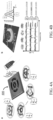
- FIGS. 1 A- 1 F illustrate various processing steps used to form a nano-electro-mechanical systems (NEMS) tag, in accordance with one embodiment.
- NEMS nano-electro-mechanical systems
- FIG. 2 is a cross-sectional view of a NEMS tag, in accordance with another exemplary embodiment.
- FIG. 3 illustrates a scanning electron microscope (SEM) image of an exemplary NEMS tag, in accordance with some embodiments.
- FIGS. 4 A- 4 B illustrate an exemplary NEMS tag concept and its topography, in accordance with some embodiments.
- FIGS. 5 A- 5 B illustrate simulated spectral signature of an exemplary NEMS tag, in accordance with some embodiments.
- FIG. 6 illustrates an exemplary method of generating a binary string for a NEMS tag, in accordance with some embodiments.
- FIG. 7 is a schematic diagram of an exemplary digital translation procedure, in accordance with some embodiments.
- FIG. 8 A illustrates an exemplary wireless interrogation setup and an exemplary model of a NEMS tag, in accordance with some embodiments.
- FIG. 8 B illustrates measured spectral signatures of four NEMS tags, in accordance with some embodiments.
- FIG. 8 C illustrates an SEM image of an array of NEMS tags, in accordance with some embodiments.
- FIGS. 9 A- 9 B illustrate measured spectral signature of another three NEMS tags, in accordance with some embodiments.
- FIGS. 10 A- 10 B illustrate extracted histogram for the inter-device Hamming distance for the NEMS tags and the bit error rate for the NEMS tags at different temperatures respectively, in accordance with some embodiments.
- first, second, etc. are, in some instances, used herein to describe some elements, these elements should not be limited by these terms. These terms are only used to distinguish one element from another.
- a first contact could be termed a second contact, and, similarly, a second contact could be termed a first contact, without departing from the scope of the some described embodiments.
- the first contact and the second contact are both contacts, but they are not the same contact, unless the context clearly indicates otherwise.
- the term “if” is, optionally, construed to mean “when” or “upon” or “in response to determining” or “in response to detecting,” depending on the context.
- the phrase “if it is determined” or “if [a stated condition or event] is detected” is, optionally, construed to mean “upon determining” or “in response to determining” or “upon detecting [the stated condition or event]” or “in response to detecting [the stated condition or event],” depending on the context.
- a nano-electro-mechanical tag system that exploits the electro-mechanical spectral signature as a fingerprint that is uniquified by inherent randomness in fabrication processing.
- Adaptive algorithms are developed for digital translation of the spectral signature into binary fingerprints.
- a plurality of NEMS tags, fabricated in a same batch are used to estimate the entropy of corresponding fingerprints with high accuracy.
- the NEMS tags are further examined under repetitive measurements and temperature variations to verify the consistency of fingerprints.
- Various embodiments highlight a potential of the clandestine nano-electro-mechanical tags for realization of secure identification and authentication methodology applicable to a wide range of products and consumer goods.
- Nano-scale physical unclonable functions have emerged to address substantial limitations of available identification and authentication tag technologies. Nano-PUFs exploit nano-fabrication techniques for miniaturization of static patterns that represent the data. While identification, removal and reapplication of nano-PUFs impose excessive challenges and require expensive equipment, the operation principle of these tags suffer from similar shortcomings of their macro-scale counterparts, e.g., the UPC and QR labels, such as the need to be in the line of sight and unsophisticated information storage principle.
- NEMS nano-electro-mechanical systems
- NEMS tags can be used in cluttered environment with large background noise and interference. Moreover, benefiting from the batch fabrication and small footprint, NEMS tags can be manufactured with low cost and used for a wide range of products.
- Various embodiments disclose design and implementation of clandestine NEMS tags, and their operation principle based on the use of electro-mechanical spectral signature along with mathematical algorithms for digital translation.
- FIGS. 1 A- 1 F illustrate various processing steps used to form a NEMS tag 100 , in accordance with one embodiment.
- the NEMS tag 100 is shown as including, in part, a protective layer 104 , a first conductive layer 106 , a piezoelectric layer 108 , a second conductive layer 110 , and one or more trenches 112 .
- NEMS tag 100 is fabricated by forming a piezoelectric layer between two metallic layers.
- the constituent layers e.g., the protective layer 104 , the first conductive layer 106 , the piezoelectric layer 108 and the second conductive layer 110 , comprise optically transparent materials.
- a protective layer 104 is formed over a substrate 102 , as illustrated in FIG. 1 A .
- the NEMS tag 100 is implemented on a glass substrate to facilitate evaluation of the NEMS tag 100 transparency.
- the protective layer 104 is formed by an atomic layer deposition method.
- the protective layer 104 comprises a hafnia (HfO 2 ) layer which has a thickness of about 10 nanometers. The hafnia layer protects the consequent layers during subsequent fabrication steps.
- a sacrificial layer 114 is deposited on the glass substrate 102 before depositing the protective layer 104 , as illustrated in FIG. 1 A .
- the sacrificial layer 114 comprises a silicon dioxide layer (SiO 2 ).
- the first conductive layer 106 is formed over the protective layer 104 , as illustrated in FIG. 1 B .
- the first conductive layer 106 serves as a bottom electrode of the NEMS tag 100 .
- the first conductive layer 106 comprises a layer of indium tin oxide (ITO), which has a thickness of about 50 nanometers. The sputtering process of ITO is engineered to enhance electric conductivity and optical transparency of the NEMS tag 100 .
- the piezoelectric layer 108 is formed over the first conductive layer 106 , as illustrated in FIG. 1 B .
- the piezoelectric layer 108 comprises a layer of scandium-doped aluminum nitride, Sc 0.3 Al 0.7 N, which has a thickness of about 100 nanometers.
- the scandium-doped aluminum nitride can be sputtered over the first conductive layer 106 .
- the scandium-doped aluminum nitride layer provides a large electromechanical coupling coefficient, which enables efficient excitation of mechanical resonance modes with minuscule electromagnetic powers.
- the piezoelectric layer 108 is patterned to expose one or more portions of the first conductive layer 106 and to provide one or more accesses to the first conductive layer 106 , as illustrated in FIG. 1 C .
- the second conductive layer 110 is formed over the piezoelectric layer 108 .
- the second conductive layer 110 is patterned to form a top electrode of the NEMS tag 100 , as illustrated in FIG. 1 D .
- the patterning of the piezoelectric layer 108 can be carried out before forming the second conductive layer 110 .
- the patterning of the piezoelectric layer 108 can be carried out after forming and patterning the second conductive layer 110 .
- the NEMS tag 100 is patterned by forming one or more trenches 112 , and the one or more trenches 112 is formed by etching through the stack above the sacrificial layer 114 , as illustrated in FIG. 1 E .
- the sacrificial layer 114 over the substrate 102 is removed to release the NEMS tag, as illustrated in FIG. 1 F .
- the sacrificial layer 114 is removed via an etching process.
- a hydrofluoric acid solution can be used as an etchant to remove the sacrificial layer 114 .
- portions of the substrate 102 may also be removed.
- the first conductive layer 106 and the second conductive layer 110 comprise a same material.
- at least one of the first conductive layer 106 , and the second conductive layer 110 are formed by a sputtering technique.
- the NEMS tag may not be released from the substrate.
- FIG. 2 is a cross-sectional view of a NEMS tag 200 , in accordance with another exemplary embodiment.
- NEMS tag 200 trench(es) 112 is formed by etching through the stack above the protective layer 104 . It is understood that FIG. 2 does not show the remaining elements (e.g., accesses to the first conductive layer) of the NEMS tag.
- the NEMS tag 100 uses an electromechanical spectral signature as the physical characteristic for identification.
- a lateral geometry of the NEMS tag 100 is designed to ensure creation of a large set of high Q mechanical resonance modes within a frequency range of interest.
- FIG. 3 illustrates an SEM image of an exemplary NEMS tag 300 , in accordance with some embodiments.
- the NEMS tag 300 comprises a first conductive layer 306 , a top electrode 314 , a piezoelectric layer 308 , one or more trenches 312 .
- the piezoelectric layer 308 is patterned to expose the first conductive layer 306 , and the exposed first conductive layer serves as a bottom electrode.
- the top electrode 314 is obtained by patterning a second conductive layer formed above the piezoelectric layer 308 .
- the NEMS tag 300 comprises one or more dummy electrodes 316 .
- the one or more dummy electrodes 316 can help achieve structure symmetry of the NEMS tag 300 .
- the NEMS tag 300 comprises an integrated coil antenna 318 .
- the coil antenna 318 can be formed by patterning the second conductive layer.
- the coil antenna 318 couples the top electrode 314 to the bottom electrode, and enables wireless interrogation of the spectral signature of the NEMS tag 300 through magnetic coupling. It is understood that FIG. 3 does not show the remaining elements (e.g., the protective layer) of the NEMS tag.
- a titanium layer with a thickness of about 10 nanometers is sputtered on the sample to enable high resolution SEM imaging.
- FIGS. 4 A- 4 B illustrate a NEMS tag concept and its topography, according to some embodiments.
- a set of mechanical resonance modes of a NEMS tag 400 with different frequency ( 0 , quality factor (Q), and vibration amplitude (A) are excited upon wireless interrogation.
- the resulting spectral signature is translated to a digital string, as illustrated in FIG. 4 B .
- a topography of a fabricated NEMS tag, integrated on a glass substrate is illustrated in FIG. 4 B .
- the fabrication uncertainties including film thickness variation, lithographical errors, and randomized crystal polymorphism induces inhomogeneous variations in spectral signature of NEMS tags and results in realization of digital strings unique to each NEMS tag.
- FIGS. 5 A- 5 B illustrate simulated spectral signature of an exemplary NEMS tag, in accordance with some embodiments.
- a large number of high Q resonance peaks is highlighted within a small frequency range over about 10 MHz to about 70 MHz.
- Different characteristics of the corresponding peaks to these resonance modes can be used to assign a binary string to the NEMS tag. These characteristics include the frequency, Q and amplitude of the peaks. All these characteristics are highly sensitive to the uncertainties during fabrication processing of the NEMS tag. Due to their random distribution, fabrication uncertainties enable natural creation of visually identical NEMS tag with unique and distinct fingerprints within a single batch. While such distinction cannot be identified visually, and is only reflected in the spectral signature, reverse engineering of the NEMS tag is challenging.
- the fabrication uncertainties that account for creation of distinct fingerprints are due to variations in device implementation, e.g., extrinsic, or inherent to material properties, e.g., intrinsic.
- the extrinsic uncertainties include one or more of a thickness variation of the constituent films, and lithography errors in patterning electrodes and device lateral geometry.
- the intrinsic uncertainties correspond to the variations in material properties that affect the spectral signature of the NEMS tag, which can include one or more of elastic constants, a mass density, and a crystal morphology of the constituent films. While the extrinsic uncertainties depend on the manufacturing facility used for implementation of the NEMS tag, the intrinsic uncertainties are inherent to the materials and define the ultimate entropy of the labels extracted for each tag.
- the Sc 0.3 Al 0.7 N film used for implementation of the NEMS tag provides large intrinsic uncertainties, due to purely randomized formation of the cubic conical clusters within hexagonal grains. This inherent characteristic corresponds to the tendency film morphology transition from hexagonal aluminum nitride (AlN) to cubic scandium nitride (ScN) at high concentration of scandium doping.
- FIG. 5 B shows cubic conical clusters that are emerged after etching the hexagonal grains of Sc 0.3 Al 0.7 N, in accordance with some embodiments. Benefiting from ultra-miniaturized size of the NEMS tags, the random distribution of these clusters within the film translates to a large entropy of the corresponding binary string.
- translation procedure for generation of binary strings corresponding to a NEMS tag relies on identification of the resonance peaks within the spectral signature and the use of their frequency.
- the procedure starts with the identification of a master spectral signature extracted from simulations, or an arbitrary tag.
- the master signature is then used as a reference to extract the decimal frequency mismatch of all the peaks within the signature of the tag.
- one or more resonance peaks are identified from a measured spectral response of the NEMS tag (i.e. the spectral signature of the NEMS tag).
- the frequency of the one or more resonance peaks is subtracted from one or more corresponding peaks in the simulated spectral signature (i.e.
- the master spectral signature resulting in a set of decimal numbers assigned to the one or more resonance peaks.
- the decimal numbers are converted to binary, and cascaded to form an initial string assigned to the NEMS tag.
- the initial binary string is shortened to a length that only contains significant bits.
- FIG. 6 illustrates an exemplary method of generating a binary string for a NEMS tag, in accordance with some embodiments.
- the method comprises identifying one or more resonance peaks within a spectral signature of the NEMS tag, as represented by block 602 .
- the spectral signature of the NEMS tag is a measured spectral signature of the NEMS tag.
- the spectral signature of the NEMS tag can be measured using a network analyzer.
- the method comprises identifying a master spectral signature, as represented by block 604 .
- the master spectral signature can be extracted from simulation of the NEMS tag.
- the master spectral signature can be extracted from a spectral signature measurement of an arbitrary NEMS tag.
- the arbitrary NEMS tag and the NEMS tag are fabricated in the same batch.
- the method comprises identifying one or more peaks in the master spectral signature corresponding to the one or more peaks identified in the spectral signature of the NEMS tag, as represented by block 606 .
- the method comprises determining frequency mismatch of the one or more peaks identified in the spectral signature of the NEMS tag and the corresponding peaks identified in the master spectral signature, as represented by block 608 .
- the frequency mismatch comprises a set of decimal numbers assigned to the one or more peaks identified in the spectral signature of the NEMS tag, and each decimal number represents a difference between one of the one or more peaks identified in the spectral signature of the NEMS tag and the corresponding peak in the master spectral signature.
- the method comprises generating the binary string corresponding to the NEMS tag based at least in part on the determined frequency mismatch, as represented by block 610 .
- the binary string is generated by converting the set of decimal numbers to binary numbers (or binary substrings) and cascading them.
- the binary string can be shortened to an optimum length that only contain significant bits.
- the leftmost bit of each substring can be assigned to the sign of the subtraction between a peak in the master spectral signature and the corresponding peak in the spectral signature of the NEMS tag. In some embodiments, additional zeros can be added to some substrings to ensure consistent length of the substrings.
- FIG. 7 is a schematic diagram of an exemplary digital translation procedure, in accordance with some embodiments.
- This digital translation procedure is used to designate unique binary tags to a NEMS tag.
- the measured spectral response of the NEMS tag is compared with a reference spectral signature.
- the reference spectral signature is generated using simulations based on a finite element method (FEM).
- FEM finite element method
- the reference spectral signature can be generated by COMSOL simulations, which provides a simulated response of the NEMS tag.
- the comparison intervals are defined by identification of the boundaries at the average frequency of the two adjacent peaks in the simulated response. In each interval, the measured spectral response of the NEMS tag is monitored to identify the dip with the highest magnitude.
- the frequency of this dip is then subtracted from its counterpart in the simulated reference signature.
- the resulting decimal value is converted to a binary string.
- the leftmost bit of the binary string defines the sign of the resulting decimal value.
- additional bits with 0 values are added to ensure a constant length of the binary string in each interval, regardless of the frequency offset between the simulated and measured values.
- all zeros are assigned to an interval when there is no measured peak in the interval.
- the binary strings corresponding to all intervals are cascaded to create the designated binary tag for the NEMS tag.
- the spectral signatures of the NEMS tags are measured using near-field wireless interrogation.
- the near-field wireless interrogation is over the frequency span from about 80 MHz to about 90 MHz.
- an ICR magnetic near-field microprobe with a coil radius of 50 ⁇ m, is positioned atop the NEMS tag to enable wireless interrogation through magnetic coupling.
- the microprobe is positioned at a sub-2-mm vertical distance from the tag and connected to a network analyzer to enable measurement of the reflection response (i.e., S11) over the 80-90-MHz spectrum. Prior to the measurement, a calibration procedure is carried out to de-embed the impedance-loading effect of the microprobe on the spectral response.
- FIG. 8 A illustrates an exemplary wireless interrogation setup and an exemplary model of a NEMS tag, in accordance with some embodiments.
- the model of the NEMS tag comprises an integrated coil antenna, a capacitor representing the piezoelectric transducer, and N mechanical RLC motional branches corresponding to different resonance modes.
- the inset shows the optical image of the device under test, as well as the corresponding vibration patterns at different resonance frequencies extracted using optical probing.
- the static response corresponding to the electrical feedthrough induced by the magnetic coupling coils and piezoelectric film capacitor is de-embedded using non-released NEMS tags.
- FIG. 8 B illustrates measured spectral signatures of four NEMS tags, in accordance with some embodiments.
- the four NEMS tags are randomly picked from an array of NEMS tags with the same layouts implemented in the same batch on a glass of substrate.
- FIG. 8 C illustrates an SEM image of the array of NEMS tags.
- the significant distinction between the vibration patterns corresponds to the different surface and bulk acoustic waves that create the resonance modes. This distinction is responsible for the highly randomized effect of intrinsic and extrinsic uncertainties on the spectral signature of the NEMS tags.
- FIG. 8 B also shows the corresponding binary labels for the four tags extracted using the digital translation procedure.
- the 31-bit string assigned to the spectral signature fingerprints highlights the large entropy of the clandestine NEMS technology, which makes it suitable for identification, authentication, and tracking applications.
- FIGS. 9 A- 9 B illustrate measured spectral signature of another three NEMS tags, in accordance with some embodiments.
- the spectral signature of the NEMS tag is measured using contact probes and a vector network analyzer to enable measurement of the transmission response (i.e., S21) over the spectrum from about 75 MHz to about 100 MHz.
- FIG. 9 A compares the frequency response of three different NEMS tags with the same layouts, which are fabricated in the same batch.
- FIG. 9 B shows corresponding vibration patterns at different resonance frequencies which are extracted using optical probing.
- a 54-bit string is designated to the spectral signature fingerprints of each NEMS tag to highlight the large entropy of the clandestine NEMS tag to enable the NEMS tag for identification, authentication, and tracking applications.
- a plurality of NEMS tags with identical designs are used.
- the inter-device Hamming distance is used as a metric to measure uniqueness of the binary strings corresponding to spectral signatures.
- FIG. 10 A illustrate extracted histogram for the inter-device Hamming distance for the NEMS tags, in accordance with some embodiments.
- the Hamming distance is extracted from a group of ten identical NEMS tags.
- the NEMS tags are also measured at across temperature variations to identify their environmental robustness.
- the temperature sensitivity of material properties and device dimensions results in finite variation of the frequency of mechanical resonance modes.
- the plurality of NEMS tags are measured over a temperature range from about ⁇ 20° C. to 100° C., in 20° C. increments, and their corresponding binary string are compared to extract the bit error rate (BER).
- BER bit error rate
- the temperature characterization is performed on a single device and in three consecutive cycles to further evaluate robustness of the binary NEMS tags over repeated measurements.
- FIG. 10 B shows the average BER at different temperatures, in accordance with some embodiments.
- the error bar at each data point shows the distribution of the BER over the three measurement cycles.
- a BER lower than about 8% is measured over ⁇ 20° C. to 100° C., which highlights the temperature stability of the NEMS tags for practical applications.
- the BER variation across measurement repetition is smaller than about ⁇ 3% over the entire temperature range, which indicates the robustness of the NEMS tags.
- TCF temperature coefficient of frequency
Landscapes
- Engineering & Computer Science (AREA)
- Manufacturing & Machinery (AREA)
- Microelectronics & Electronic Packaging (AREA)
- Chemical & Material Sciences (AREA)
- Inorganic Chemistry (AREA)
- Investigating Or Analysing Materials By Optical Means (AREA)
- Measurement Of The Respiration, Hearing Ability, Form, And Blood Characteristics Of Living Organisms (AREA)
Abstract
Description
Claims (20)
Priority Applications (1)
| Application Number | Priority Date | Filing Date | Title |
|---|---|---|---|
| US17/152,294 US11873214B2 (en) | 2020-01-21 | 2021-01-19 | Nano-electro-mechanical tags for identification and authentication |
Applications Claiming Priority (2)
| Application Number | Priority Date | Filing Date | Title |
|---|---|---|---|
| US202062964014P | 2020-01-21 | 2020-01-21 | |
| US17/152,294 US11873214B2 (en) | 2020-01-21 | 2021-01-19 | Nano-electro-mechanical tags for identification and authentication |
Publications (2)
| Publication Number | Publication Date |
|---|---|
| US20210221675A1 US20210221675A1 (en) | 2021-07-22 |
| US11873214B2 true US11873214B2 (en) | 2024-01-16 |
Family
ID=76857709
Family Applications (1)
| Application Number | Title | Priority Date | Filing Date |
|---|---|---|---|
| US17/152,294 Active 2042-09-10 US11873214B2 (en) | 2020-01-21 | 2021-01-19 | Nano-electro-mechanical tags for identification and authentication |
Country Status (1)
| Country | Link |
|---|---|
| US (1) | US11873214B2 (en) |
Citations (2)
| Publication number | Priority date | Publication date | Assignee | Title |
|---|---|---|---|---|
| US20120274647A1 (en) * | 2011-04-26 | 2012-11-01 | Qualcomm Mems Technologies, Inc. | Piezoelectric resonators and fabrication processes |
| US11569431B1 (en) * | 2019-08-19 | 2023-01-31 | National Technology & Engineering Solutions Of Sandia, Llc | Piezoelectric deformable photonic devices |
-
2021
- 2021-01-19 US US17/152,294 patent/US11873214B2/en active Active
Patent Citations (2)
| Publication number | Priority date | Publication date | Assignee | Title |
|---|---|---|---|---|
| US20120274647A1 (en) * | 2011-04-26 | 2012-11-01 | Qualcomm Mems Technologies, Inc. | Piezoelectric resonators and fabrication processes |
| US11569431B1 (en) * | 2019-08-19 | 2023-01-31 | National Technology & Engineering Solutions Of Sandia, Llc | Piezoelectric deformable photonic devices |
Also Published As
| Publication number | Publication date |
|---|---|
| US20210221675A1 (en) | 2021-07-22 |
Similar Documents
| Publication | Publication Date | Title |
|---|---|---|
| CN109074371B (en) | Method and computing device for determining whether a mark is authentic | |
| RU2648582C1 (en) | Ways and computer device for determining whether the sign is the authentic | |
| US9121873B2 (en) | Electronic circuit component authenticity determination method | |
| Bernstein et al. | High Q diamond hemispherical resonators: Fabrication and energy loss mechanisms | |
| Willers et al. | MEMS gyroscopes as physical unclonable functions | |
| CN101472835B (en) | Methods and systems for object recognition and authentication | |
| Satpal et al. | Damage identification in aluminum beams using support vector machine: Numerical and experimental studies | |
| Du et al. | Unclonable optical fiber identification based on Rayleigh backscattering signatures | |
| Zhang et al. | Random Nanofracture‐Enabled Physical Unclonable Function | |
| JP2008135446A (en) | Method of producing rf powder | |
| US20220116233A1 (en) | Device tracking or verifiwatermarking for electroniccation | |
| US20200186368A1 (en) | Generating a nondeterministic response to a challenge | |
| EP3698512A1 (en) | Unique identifiers based on quantum effects | |
| Jang et al. | Real‐Time Endpoint Detection of Small Exposed Area Si O 2 Films in Plasma Etching Using Plasma Impedance Monitoring with Modified Principal Component Analysis | |
| JP2009521040A (en) | Security element, manufacturing method thereof and authentication method | |
| US11873214B2 (en) | Nano-electro-mechanical tags for identification and authentication | |
| CN120164221A (en) | Online real-time image recognition anti-counterfeiting verification method and system based on gold trading | |
| Yang et al. | UCR: An unclonable environmentally sensitive chipless RFID tag for protecting supply chain | |
| US10586135B2 (en) | Nano-electro-mechanical labels and encoder | |
| Hüttel et al. | Single electron tunnelling through high‐Q single‐wall carbon nanotube NEMS resonators | |
| Valavi et al. | Physically unclonable functions based on small delay defects in QCA | |
| JP2019220869A (en) | Data generation device, authentication device, and authentication system | |
| Udaya Shankar et al. | A review on machine learning based counterfeit integrated circuit detection | |
| US10922503B2 (en) | Multi frequency signatures using nano/microscale three dimensional printed structures | |
| Ali et al. | Detection of minimum geometrical variation by free-space-based chipless approach and its application to authentication |
Legal Events
| Date | Code | Title | Description |
|---|---|---|---|
| FEPP | Fee payment procedure |
Free format text: ENTITY STATUS SET TO UNDISCOUNTED (ORIGINAL EVENT CODE: BIG.); ENTITY STATUS OF PATENT OWNER: SMALL ENTITY |
|
| FEPP | Fee payment procedure |
Free format text: ENTITY STATUS SET TO SMALL (ORIGINAL EVENT CODE: SMAL); ENTITY STATUS OF PATENT OWNER: SMALL ENTITY |
|
| STPP | Information on status: patent application and granting procedure in general |
Free format text: APPLICATION DISPATCHED FROM PREEXAM, NOT YET DOCKETED |
|
| AS | Assignment |
Owner name: UNIVERSITY OF FLORIDA RESEARCH FOUNDATION, INCORPORATED, FLORIDA Free format text: ASSIGNMENT OF ASSIGNORS INTEREST;ASSIGNORS:TABRIZIAN, ROOZBEH;BHUNIA, SWARUP;SIGNING DATES FROM 20210120 TO 20210125;REEL/FRAME:055696/0600 |
|
| STPP | Information on status: patent application and granting procedure in general |
Free format text: DOCKETED NEW CASE - READY FOR EXAMINATION |
|
| STPP | Information on status: patent application and granting procedure in general |
Free format text: NOTICE OF ALLOWANCE MAILED -- APPLICATION RECEIVED IN OFFICE OF PUBLICATIONS |
|
| STPP | Information on status: patent application and granting procedure in general |
Free format text: PUBLICATIONS -- ISSUE FEE PAYMENT RECEIVED |
|
| STPP | Information on status: patent application and granting procedure in general |
Free format text: PUBLICATIONS -- ISSUE FEE PAYMENT VERIFIED |
|
| STCF | Information on status: patent grant |
Free format text: PATENTED CASE |