US11868563B2 - Touch panel device, touch panel control method, and storage medium storing touch panel control program - Google Patents
Touch panel device, touch panel control method, and storage medium storing touch panel control program Download PDFInfo
- Publication number
- US11868563B2 US11868563B2 US17/680,736 US202217680736A US11868563B2 US 11868563 B2 US11868563 B2 US 11868563B2 US 202217680736 A US202217680736 A US 202217680736A US 11868563 B2 US11868563 B2 US 11868563B2
- Authority
- US
- United States
- Prior art keywords
- touch
- sensor unit
- capacitance
- touch panel
- unit
- Prior art date
- Legal status (The legal status is an assumption and is not a legal conclusion. Google has not performed a legal analysis and makes no representation as to the accuracy of the status listed.)
- Active
Links
Images


Classifications
-
- G—PHYSICS
- G06—COMPUTING OR CALCULATING; COUNTING
- G06F—ELECTRIC DIGITAL DATA PROCESSING
- G06F3/00—Input arrangements for transferring data to be processed into a form capable of being handled by the computer; Output arrangements for transferring data from processing unit to output unit, e.g. interface arrangements
- G06F3/01—Input arrangements or combined input and output arrangements for interaction between user and computer
- G06F3/03—Arrangements for converting the position or the displacement of a member into a coded form
- G06F3/041—Digitisers, e.g. for touch screens or touch pads, characterised by the transducing means
- G06F3/0416—Control or interface arrangements specially adapted for digitisers
- G06F3/0418—Control or interface arrangements specially adapted for digitisers for error correction or compensation, e.g. based on parallax, calibration or alignment
-
- G—PHYSICS
- G06—COMPUTING OR CALCULATING; COUNTING
- G06F—ELECTRIC DIGITAL DATA PROCESSING
- G06F3/00—Input arrangements for transferring data to be processed into a form capable of being handled by the computer; Output arrangements for transferring data from processing unit to output unit, e.g. interface arrangements
- G06F3/01—Input arrangements or combined input and output arrangements for interaction between user and computer
- G06F3/03—Arrangements for converting the position or the displacement of a member into a coded form
- G06F3/041—Digitisers, e.g. for touch screens or touch pads, characterised by the transducing means
- G06F3/044—Digitisers, e.g. for touch screens or touch pads, characterised by the transducing means by capacitive means
- G06F3/0443—Digitisers, e.g. for touch screens or touch pads, characterised by the transducing means by capacitive means using a single layer of sensing electrodes
-
- G—PHYSICS
- G06—COMPUTING OR CALCULATING; COUNTING
- G06F—ELECTRIC DIGITAL DATA PROCESSING
- G06F3/00—Input arrangements for transferring data to be processed into a form capable of being handled by the computer; Output arrangements for transferring data from processing unit to output unit, e.g. interface arrangements
- G06F3/01—Input arrangements or combined input and output arrangements for interaction between user and computer
- G06F3/03—Arrangements for converting the position or the displacement of a member into a coded form
- G06F3/041—Digitisers, e.g. for touch screens or touch pads, characterised by the transducing means
- G06F3/044—Digitisers, e.g. for touch screens or touch pads, characterised by the transducing means by capacitive means
- G06F3/0447—Position sensing using the local deformation of sensor cells
-
- G—PHYSICS
- G06—COMPUTING OR CALCULATING; COUNTING
- G06F—ELECTRIC DIGITAL DATA PROCESSING
- G06F2203/00—Indexing scheme relating to G06F3/00 - G06F3/048
- G06F2203/041—Indexing scheme relating to G06F3/041 - G06F3/045
- G06F2203/04105—Pressure sensors for measuring the pressure or force exerted on the touch surface without providing the touch position
Definitions
- a property e.g., viscosity or rigidity
- An object of the present disclosure which has been made to resolve the above-described problem with the conventional technology, is to provide a touch panel device, a touch panel control method and a touch panel control program capable of inhibiting the occurrence of the erroneous judgment on a touch operation due to temperature variations.
- a touch panel device includes a cover panel that has an operation surface on which a touch operation is performed and bends corresponding to a depressing force applied to the operation surface; a touch sensor unit including touch sensor electrodes that output touch sensor signals corresponding to the touch operation; an elastic member that has a dielectric constant changing corresponding to a temperature and deforms due to the bending of the cover panel, the elastic member including an adhesive agent provided between the cover panel and the touch sensor unit; a first sensor unit that detects a capacitance changing depending on the dielectric constant and a thickness of the elastic member; and processing circuitry to estimate the temperature based on the capacitance detected by the first sensor unit; to detect the depressing force based on the estimated temperature and the capacitance detected by the first sensor unit; and to execute processing of the touch sensor signals based on the detected depressing force.
- a touch panel control method is a touch panel control method executed by a touch panel device that includes a cover panel that has an operation surface on which a touch operation is performed and bends corresponding to a depressing force applied to the operation surface, a touch sensor unit including touch sensor electrodes that output touch sensor signals corresponding to the touch operation, an elastic member that has a dielectric constant changing corresponding to a temperature and deforms due to the bending of the cover panel, the elastic member including an adhesive agent provided between the cover panel and the touch sensor unit, and a first sensor unit that detects a capacitance changing depending on the dielectric constant and a thickness of the elastic member.
- the method includes estimating the temperature based on the capacitance detected by the first sensor unit; detecting the depressing force based on the estimated temperature and the capacitance detected by the first sensor unit; and executing processing of the touch sensor signals based on the detected depressing force.
- FIGS. 1 A and 1 B are cross-sectional views schematically showing the structure of a touch panel device according to a first embodiment of the present disclosure
- FIG. 2 is an enlarged sectional view schematically showing the structure of a principal part of the touch panel device according to the first embodiment
- FIG. 3 is an enlarged sectional view schematically showing the structure of the principal part of the touch panel device according to the first embodiment
- FIG. 4 is a plan view schematically showing the touch panel device according to the first embodiment
- FIG. 5 is a functional block diagram schematically showing the configuration of a control unit of the touch panel device according to the first embodiment
- FIG. 6 is a diagram showing an example of the hardware configuration of the touch panel device according to the first embodiment
- FIG. 7 is a diagram showing another example of the hardware configuration of the touch panel device according to the first embodiment.
- FIG. 8 is a flowchart showing the operation of the touch panel device according to the first embodiment
- FIG. 9 is an enlarged sectional view schematically showing the structure of a principal part of a touch panel device according to a first modification of the first embodiment
- FIG. 10 is an enlarged sectional view schematically showing the structure of a principal part of a touch panel device according to a second modification of the first embodiment
- FIG. 11 is an enlarged sectional view schematically showing the structure of a principal part of a touch panel device according to a third modification of the first embodiment
- FIG. 12 is an enlarged sectional view schematically showing the structure of a principal part of a touch panel device according to a fourth modification of the first embodiment
- FIG. 13 is a functional block diagram schematically showing the configuration of a control unit of a touch panel device according to a second embodiment of the present disclosure
- FIGS. 14 A and 14 B are graphs showing a temperature characteristic of a relative dielectric constant when 1 kHz AC voltage is applied and when 100 kHz AC voltage is applied;
- FIG. 15 is a flowchart showing the operation of the touch panel device according to a second embodiment
- FIG. 16 A is a cross-sectional view schematically showing the structure of a touch panel device according to a third embodiment of the present disclosure
- FIGS. 16 B and 16 C are diagrams showing a differential circuit included in a dielectric constant comparison unit
- FIG. 17 is a functional block diagram schematically showing the configuration of a control unit of the touch panel device according to the third embodiment.
- FIG. 19 is a diagram showing the operation of a differential circuit used in the touch panel device of FIGS. 18 A and 18 B ;
- FIG. 21 is a diagram showing another example of the hardware configuration of the touch panel device according to the third embodiment.
- FIGS. 22 A and 22 B are cross-sectional views schematically showing the structure of a touch panel device according to a fourth embodiment of the present disclosure.
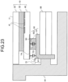
- FIG. 23 is an enlarged sectional view schematically showing the structure of a principal part of the touch panel device according to the fourth embodiment.
- FIG. 24 is a functional block diagram schematically showing the configuration of a control unit of the touch panel device according to the fourth embodiment.
- FIGS. 25 A to 25 D are diagrams showing the operation of the touch panel device according to the fourth embodiment.
- FIG. 27 is a diagram showing another example of the hardware configuration of the touch panel device according to the fourth embodiment.
- FIG. 28 is a flowchart showing the operation of the touch panel device according to the fourth embodiment.
- FIG. 29 is an enlarged sectional view schematically showing the structure of a principal part of the touch panel device according to a fifth embodiment.
- FIG. 30 is a plan view schematically showing the touch panel device according to the fifth embodiment.
- FIGS. 1 A and 1 B are cross-sectional views schematically showing the structure of a touch panel device 1 according to a first embodiment.
- FIG. 1 A shows a state in which no touch operation is being performed on an operation surface 11 of the touch panel device 1 .
- FIG. 1 B shows a state in which a touch operation is being performed while applying a depressing force to the operation surface 11 of the touch panel device 1 with a finger 700 .
- FIG. 2 is an enlarged sectional view schematically showing the structure of a principal part of the touch panel device 1 .
- FIG. 2 shows a state in which no touch operation is being performed on the operation surface 11 of the touch panel device 1 .
- FIG. 3 is an enlarged sectional view schematically showing the structure of the principal part of the touch panel device 1 .
- FIG. 3 shows a state in which a touch operation is being performed while applying a depressing force to the operation surface 11 of the touch panel device 1 .
- FIG. 4 is a plan view schematically showing the touch panel device 1 .
- the touch panel device 1 includes a cover panel 20 , a touch sensor unit 40 , an adhesive agent 30 as an elastic member, and a first sensor unit 61 .
- the cover panel 20 and the touch sensor unit 40 are bonded to each other by the adhesive agent 30 .
- the cover panel 20 , the touch sensor unit 40 and the adhesive agent 30 constitute a touch panel unit 10 .
- the touch panel device 1 includes a display panel unit 80 , a frame 81 included in the display panel unit 80 , and an elastic material 50 as an elastic member provided between the display panel unit 80 and the touch panel unit 10 .
- the elastic material 80 is a dielectric substance.
- the cover panel 20 has the operation surface 11 on which a touch operation is performed by use of an electric conductor such as the finger 700 . As shown in FIGS. 1 B and 3 , the cover panel 20 bends corresponding to the depressing force applied to the operation surface 11 . In other words, the whole of the cover panel 20 slightly curves corresponding to the depressing force applied to the operation surface 11 .
- the cover panel 20 is transparent glass, for example.
- the cover panel 20 is referred to also as protective glass.
- the cover panel 20 is supported by a housing 90 .
- the structure in which the cover panel 20 is fixed to the housing 90 is referred to also as compression mount structure.
- the touch sensor unit 40 is a touch sensor panel which is a plate-like device, for example.
- the touch sensor unit 40 includes a plurality of touch sensor electrodes 41 that output touch sensor signals corresponding to a touch operation performed by use of an electric conductor.
- the touch sensor signal is a signal corresponding to an electrostatic capacitance of a touch sensor electrode 41 changed by the touch operation.
- the touch sensor electrode 41 is formed with ITO (Indium Tin Oxide) being a transparent electrode, for example.
- the adhesive agent 30 is a dielectric substance.
- the dielectric constant of the adhesive agent 30 changes corresponding to the temperature.
- the adhesive agent 30 is an elastic member that deforms due to the bending of the cover panel 20 .
- the adhesive agent 30 can also be an adhesive sheet.
- the first sensor unit 61 is a first sensor set including one or more capacitance sensors.
- the first sensor unit 61 includes a first capacitance sensor that detects a capacitance C 61 that changes depending on the dielectric constant of the adhesive agent 30 and the thickness of the adhesive agent 30 .
- the first sensor unit 61 includes a first displacement detection electrode 61 a and a second displacement detection electrode 61 b arranged at positions to face each other across the adhesive agent 30 .
- the first displacement detection electrode 61 a and the second displacement detection electrode 61 b are formed with ITO, for example.
- the first displacement detection electrode 61 a is arranged on a surface of the touch sensor unit 40 on the adhesive agent 30 's side.
- the second displacement detection electrode 61 b is arranged on a surface of the cover panel 20 on the adhesive agent 30 's side.
- the first sensor unit 61 includes four first capacitance sensors.
- the number of first capacitance sensors is not limited to four.
- the display panel unit 80 displays an image that is visible through the touch panel unit 10 .
- the display panel unit 80 displays an image such as a GUI (Graphical User Interface), for example.
- the display panel unit 80 is, for example, a liquid crystal panel unit including a liquid crystal display and a backlight unit.
- FIG. 5 is a functional block diagram schematically showing the configuration of a control unit 100 of the touch panel device 1 .
- the touch panel device 1 includes the control unit 100 .
- the control unit 100 is capable of executing a touch panel control method according to the first embodiment.
- the control unit 100 can also be a part of an information processing device such as a computer that executes a touch panel control program according to the first embodiment.
- the control unit 100 includes a touch detection unit 101 , an AC voltage application unit 102 , a dielectric constant detection unit 103 , a temperature estimation unit 104 , a temperature characteristic information storage unit 105 , a depressing force detection unit 106 and a touch operation judgment unit 107 .
- the temperature characteristic information storage unit 105 may also be included in an external device different from the touch panel device 1 .
- the touch detection unit 101 receives a plurality of touch sensor signals outputted from a plurality of touch sensor electrodes 41 and provides the temperature estimation unit 104 with a touch detection signal based on the plurality of touch sensor signals.
- the touch detection signal includes, for example, a coordinate signal indicating a touch position as the position of the touch operation on the operation surface 11 .
- the AC voltage application unit 102 supplies an AC voltage at a predetermined frequency to the first displacement detection electrode 61 a of the first sensor unit 61 .
- the dielectric constant detection unit 103 obtains the dielectric constant from the detection value of the capacitance C 61 outputted from the first sensor unit 61 and supplies the temperature estimation unit 104 with a signal indicating the dielectric constant of the adhesive agent 30 being the elastic member.
- the temperature estimation unit 104 estimates the temperature of the adhesive agent 30 based on the capacitance C 61 detected by the first sensor unit 61 .
- the temperature estimation unit 104 estimates the temperature of the adhesive agent 30 based on the dielectric constant calculated based on the detection value of the capacitance C 61 outputted from the first sensor unit 61 .
- temperature characteristic information previously stored in the temperature characteristic information storage unit 105 is referred to.
- the temperature characteristic information is, for example, information indicating a correspondence relationship between the dielectric constant and the temperature.
- the depressing force detection unit 106 detects (e.g., calculates) the depressing force based on the temperature estimated by the temperature estimation unit 104 and the capacitance C 61 detected by the first sensor unit 61 . Specifically, when the depressing force detection unit 106 detects (e.g., calculates) the depressing force based on the capacitance C 61 detected by the first sensor unit 61 , the depressing force detection unit 106 outputs a depressing force corrected by using the temperature estimated by the temperature estimation unit 104 .
- the touch operation judgment unit 107 executes processing of the touch sensor signals by using the depressing force outputted from the depressing force detection unit 106 . For example, the touch operation judgment unit 107 judges whether or not the touch operation is a touch operation with a depressing force greater than or equal to a predetermined reference value. Specifically, the touch operation judgment unit 107 judges that the touch operation is a valid touch operation when the touch operation is a touch operation with a depressing force greater than or equal to the predetermined reference value, and judges that the touch operation is an invalid touch operation when the depressing force at the time when the touch operation is performed is less than the predetermined reference value.
- the reason why the depressing force detection unit 106 refers to the temperature estimated by the temperature estimation unit 104 is that a property (e.g., rigidity or elasticity) of the adhesive agent 30 being the elastic member changes depending on the temperature.
- a property e.g., rigidity or elasticity
- the adhesive agent 30 becomes more likely to be deformed with the increase in the temperature. Namely, even if the same depressing force is applied, the deformation of the adhesive agent 30 when the temperature is low is slight and the deformation of the adhesive agent 30 when the temperature is high is great. Further, the dielectric constant of the adhesive agent 30 being the elastic member changes depending on the temperature.
- the dielectric constant of the adhesive agent 30 is detected by the dielectric constant detection unit 103 and the first sensor unit 61 as a depressing force sensor and the temperature of the adhesive agent 30 is estimated by the temperature estimation unit 104 from the detected dielectric constant. Further, the depressing force detection unit 106 outputs a depressing force corrected by using the temperature estimated by the temperature estimation unit 104 .
- FIG. 6 is a diagram showing an example of the hardware configuration of the touch panel device 1 .
- the touch panel device 1 includes a memory 902 capable of storing a program and a processor 901 as an information processing unit that executes the program.
- the program includes the touch panel control program according to the first embodiment.
- the program can be provided by using a record medium for storing information.
- the touch panel device 1 includes the touch sensor unit 40 having a plurality of touch sensor electrodes, the first sensor unit 61 having the functions as the depressing force sensor and a dielectric constant sensor, and the display panel unit 80 .
- FIG. 7 is a diagram showing another example of the hardware configuration of the touch panel device 1 .
- the touch panel device 1 includes processing circuitry 903 .
- the control unit 100 shown in FIG. 5 can be implemented by the processing circuitry 903 .
- the touch operation judgment unit 107 executes the processing of the touch sensor signals based on the detected depressing force. For example, the touch operation judgment unit 107 executes a process of judging whether or not the detected depressing force is greater than or equal to a predetermined threshold value and executes a process based on the result of the judgment.
- FIG. 9 is an enlarged sectional view schematically showing the structure of a principal part of a touch panel device according to a first modification of the first embodiment.
- the touch panel device shown in FIG. 9 includes a first sensor unit 62 instead of the first sensor unit 61 in FIG. 1 to FIG. 4 .
- the first sensor unit 62 includes a first displacement detection electrode 62 a and the frame 81 as a second displacement detection electrode 62 b . Except for these features, the touch panel device shown in FIG. 9 is the same as the touch panel device shown in FIG. 1 to FIG. 4 .
- FIG. 10 is an enlarged sectional view schematically showing the structure of a principal part of a touch panel device according to a second modification of the first embodiment.
- the case where the elastic member is the adhesive agent 30 is described.
- the example shown in FIG. 10 illustrates a case where the elastic member is the adhesive agent 30 and the elastic material 50 .
- the touch panel device shown in FIG. 10 includes the first sensor unit 62 in addition to the first sensor unit 61 in FIG. 1 to FIG. 4 .
- the first sensor unit 62 includes the first displacement detection electrode 62 a and the frame 81 as the second displacement detection electrode.
- the dielectric constant detection unit 103 detects the dielectric constant based on a capacitance C 62 outputted f rom the first sensor unit 62 .
- the depressing force detection unit 106 detects the depressing force based on the estimated temperature and the capacitance C 62 outputted from the first sensor unit 62 . Except for these features, the touch panel device shown in FIG. 10 is the same as the touch panel device shown in FIG. 1 to FIG. 4 .
- FIG. 11 is an enlarged sectional view schematically showing the structure of a principal part of a touch panel device according to a third modification of the first embodiment.
- the touch panel device shown in FIG. 11 includes a second sensor unit 71 having detection electrodes arranged to face each other across a space adjoining the adhesive agent 30 in addition to the first sensor unit 61 in FIG. 1 to FIG. 4 .
- the second sensor unit 71 is a second sensor set including one or more capacitance sensors.
- the second sensor unit 71 includes a third displacement detection electrode 71 a and a fourth displacement detection electrode 71 b .
- the dielectric constant detection unit 103 detects the dielectric constant based on the capacitance C 61 outputted from the first sensor unit 61 and a capacitance C 71 outputted from the second sensor unit 71 .
- the depressing force detection unit 106 detects the depressing force based on the estimated temperature, the capacitance C 61 outputted from the first sensor unit 61 and the capacitance C 71 outputted from the second sensor unit 71 . Except for these features, the touch panel device shown in FIG. 11 is the same as the touch panel device shown in FIG. 1 to FIG. 4 .
- FIG. 12 is an enlarged sectional view schematically showing the structure of a principal part of a touch panel device according to a fourth modification of the first embodiment.
- the touch panel device shown in FIG. 12 includes third sensor units 72 and 73 in addition to the first sensor unit 61 and the second sensor unit 71 .
- the third sensor unit 72 is a third sensor set including one or more capacitance sensors.
- the third sensor unit 72 includes a fifth displacement detection electrode 72 a and the frame 81 as a sixth displacement detection electrode.
- the third sensor unit 73 is another third sensor set including one or more capacitance sensors.
- the third sensor unit 73 includes a seventh displacement detection electrode 73 a and the frame 81 as an eighth displacement detection electrode.
- the dielectric constant detection unit 103 detects the dielectric constant based on the capacitance C 61 outputted from the first sensor unit 61 , the capacitance C 71 outputted from the second sensor unit 71 and a capacitances C 72 and C 73 outputted from the third sensor units 72 and 73 .
- the depressing force detection unit 106 detects the depressing force based on the estimated temperature, the capacitance C 61 outputted from the first sensor unit 61 , the capacitance C 71 outputted from the second sensor unit 71 and the capacitances C 72 and C 73 outputted from the third sensor units 12 and 73 . Except for these features, the touch panel device shown in FIG. 12 is the same as the touch panel device shown in FIG. 11 .
- FIG. 13 is a functional block diagram schematically showing the configuration of a control unit 200 of a touch panel device 2 according to a second embodiment.
- each component identical or corresponding to a component shown in FIG. 5 is assigned the same reference character as in FIG. 5 .
- the control unit 200 of the touch panel device 2 differs front the control unit 100 shown in FIG. 5 in that an AC voltage application unit 102 a is capable of switching a drive frequency to a plurality of frequencies.
- the relative dielectric constant ⁇ (T 1 ) when the temperature is T 1 [° C.] and the relative dielectric constant ⁇ (T 2 ) when the temperature is T 2 [° C.] are almost the same value ⁇ (T 12 ).
- the temperature estimation unit 12 obtains two temperatures T 1 [° C.] and T 2 [° C.] as the estimation result. Therefore, in the second embodiment, the relative dielectric constant ⁇ (T 1 ) when the temperature is T 1 [° C.] and the relative dielectric constant ⁇ (T 2 ) when the temperature is T 2 [° C.] are obtained in the case of FIG. 14 B .
- the temperature estimation unit 104 is capable of distinguishing between the two temperatures T 1 [° C.] and T 2 [° C.].
- FIG. 15 is a flowchart showing the operation of the touch panel device 2 .
- the dielectric constant detection unit 103 detects the dielectric constant of the adhesive agent 30 based on the capacitance C 61 detected by the first sensor unit 61 in a state in which the AC voltage at a first drive frequency is applied thereto and provides the temperature estimation unit 104 with the detected dielectric constant.
- the dielectric constant detection unit 103 detects the dielectric constant of the adhesive agent 30 based on the capacitance C 61 detected by the first sensor unit 61 in a state in which the AC voltage at a second drive frequency different from the first drive frequency is applied thereto and provides the temperature estimation unit 104 with the detected dielectric constant.
- the temperature estimation unit 104 estimates the temperature of the adhesive agent 30 based on the received dielectric constants and the temperature characteristic information and provides the depressing force detection unit 106 with the estimated temperature.
- the processing in the subsequent steps S 13 and S 14 is the same as that in FIG. 3 .
- the detection error of the depressing force due to temperature variations can be reduced. Further, the erroneous judgments in touch operations can be reduced since the temperature can be estimated accurately even in oases where the temperature characteristic of the relative dielectric constant of the adhesive agent 30 as the elastic member is not monotonically increasing or monotonically decreasing.
- the second embodiment is the same as the first embodiment.
- FIG. 16 A is a cross-sectional view schematically showing the structure of a touch panel device 3 according to a third embodiment
- FIGS. 16 B and 16 C are diagrams showing a differential circuit included in a dielectric constant comparison unit 301 .
- the structure shown in FIG. 16 A is the same as the structure in FIG. 11 .
- the touch panel device 3 according to the third embodiment includes the first sensor unit 61 and the second sensor unit 71 .
- Each of C p0 and C p1 is a capacitance determined by the distance between electrodes and the dielectric constant.
- Each of C R0 and C R1 represents an electrical charge that is accumulated by charging shown in FIG. 16 B .
- FIG. 17 is a functional block diagram schematically showing the configuration of a control unit 300 of the touch panel device 3 according to the third embodiment.
- each component identical or corresponding to a component shown in FIG. 5 is assigned the same reference character as in FIG. 5 .
- the control unit 300 of the touch panel device 3 differs from the control unit 100 shown in FIG. 5 in including the dielectric constant comparison unit 301 and in that the temperature estimation unit 104 estimates the temperature based on a difference in the dielectric constant.
- the charging is done for an electrical charge corresponding to (C R1 +C p1 ) and an electrical charge corresponding to (C R0 +C p0 ) as shown in FIG. 16 B , and thereafter a difference (V 1 ⁇ V 0 ) between a voltage V 1 and a voltage V 0 when both electrical charges have been discharged as shown in FIG. 16 C is outputted.
- the temperature estimation unit 104 estimates the temperature based on the difference (V 1 ⁇ V 0 ).
- FIGS. 18 A and 18 B are cross-sectional views schematically showing another example of the structure of the touch panel device 3 according to the third embodiment.
- the structure shown in FIGS. 18 A and 18 B is the same as the structure in FIG. 11 .
- FIG. 19 is a diagram showing different structure of the dielectric constant comparison unit 301 .
- a difference between a capacitance C 0 and a capacitance C 1 is obtained while an applying AC voltage to the second displacement detection electrode 61 b and the fourth displacement detection electrode 71 b .
- the change in the capacitance C 1 due to a temperature change is greater than the change in the capacitance C 0 .
- the control unit 300 when a depressing force, is applied to the operation surface 11 , C 0 >C 1 holds. Furthermore, when no depressing force is applied, (C 0 ⁇ C 1 ) is constant. Therefore, when there is no touch operation, the control unit 300 is capable of obtaining the temperature from the capacitance difference (C 0 ⁇ C 1 ) in a state in which the capacitance difference (C 0 ⁇ C 1 ) changes slowly. Further, when there is a touch operation, the control unit 300 is capable of obtaining the depressing force from the capacitance difference (C 0 ⁇ C 1 ) in a state in which (C 0 ⁇ C 1 ) changes rapidly.
- FIG. 20 is a diagram showing an example of the hardware configuration of the touch panel device 3 .
- the touch panel device 3 includes a memory 902 capable of storing a program and a processor 901 as an information processing unit that executes the program.
- the control unit 300 shown in FIG. 17 can be implemented by using the memory 902 as a storage device storing the program as software and the processor 901 as the information processing unit that executes the program stored in the memory 902 .
- FIG. 21 is a diagram showing another example of the hardware configuration of the touch panel device 3 .
- the touch panel device 3 includes processing circuitry 903 .
- the control unit 300 shown in FIG. 17 can be implemented by the processing circuitry 903 .
- the detection error of the depressing force due to temperature variations can be reduced. Accordingly, the erroneous judgments in touch operations can be reduced even in cases where the temperature variations are great.
- influence of noise included in the detection value of the capacitance can be eliminated since the temperature is estimated based on the difference in the capacitance. Accordingly, the accuracy of the temperature estimation can foe increased and the erroneous judgments in touch operations can be reduced.
- the third embodiment is the same as the first embodiment.
- FIGS. 22 A and 22 B are cross-sectional views schematically showing the structure of a touch panel device 4 according to a fourth embodiment.
- FIG. 22 A shows a state in which no touch operation is being performed on the operation surface 11 of the touch panel device 4 .
- FIG. 22 B shows a state in which a touch operation is being performed while applying a depressing force to the operation surface 11 of the touch panel device 4 with the finger 700 .
- FIG. 23 is an enlarged sectional view schematically showing the structure of a principal part of the touch panel device 4 .
- FIG. 23 shows a state in which no touch operation is being performed on the operation surface 11 of the touch panel device 4 .
- the touch panel device 4 includes the cover panel 20 , the touch sensor unit 40 and the adhesive agent 30 . Further, the touch panel device 4 includes the display panel unit 80 , the frame 81 included in the display panel unit 30 , and the elastic material 50 as an elastic member provided between the display panel unit 80 and the touch panel unit 10 .
- the elastic material 50 is a dielectric substance. The dielectric constant of the elastic material 50 changes corresponding to the temperature.
- the elastic material 50 is an elastic member that deforms due to the bending of the cover panel 20 .
- the cover panel 20 has the operation surface 11 on which a touch operation is performed by use of an electric conductor such as the finger 700 . As shown in FIG. 22 B , the cover panel 20 bends corresponding to the depressing force applied to the operation surface 11 . In other words, the whole of the cover panel 20 slightly curves corresponding to the depressing force applied to the operation surface 11 .
- the cover panel 20 is not supported by a housing 91 , whereas the frame 81 and the display panel unit 80 are supported by the housing 91 .
- the structure in which the housing 91 supports the frame 81 and the display panel unit 80 is referred to also as side mount structure.
- the touch panel device 4 includes the first sensor unit 62 and the third sensor unit 72 .
- the first sensor unit 62 includes a first capacitance sensor that detects the capacitance C 62 that changes depending on the dielectric constant of the elastic material 50 and the thickness of the elastic material 50 .
- the first sensor unit 62 includes a first displacement detection electrode 62 a (i.e., a transmissive conductive film 74 ) and a second displacement detection electrode (i.e., the frame 81 ) arranged at positions to face each other across the elastic material 50 .
- the first displacement detection electrode 62 a and the second displacement detection electrode are formed with ITO, for example.
- the third sensor unit 72 includes a fifth displacement detection electrode 72 a (i.e., the transmissive conductive film 74 ) and a sixth displacement detection electrode (i.e., the frame 81 ) arranged at positions to face each other across a space adjoining the elastic material 50 .
- the fifth displacement detection electrode 72 a and the sixth displacement detection electrode are formed with ITO, for example.
- FIG. 24 is a functional block diagram schematically showing the configuration of a control unit 400 of the touch panel device 4 .
- the touch panel device 4 includes the control unit 400 .
- the control unit 400 is capable of executing a touch panel control method according to the fourth embodiment.
- the control unit 400 can also be a part of an information processing device such as a computer that executes a touch panel control program according to the fourth embodiment.
- the control unit 400 differs from the control units in the first to third embodiments in including a transmissive conductive film detection unit 401 that detects the capacitance of the transmissive conductive film 74 and provides the temperature estimation unit 104 with the detection value of the capacitance and in including a transmissive conductive film control unit 402 that supplies electric power to the transmissive conductive film and thereby makes the transmissive conductive film 74 operate as a heater.
- FIGS. 25 A to 25 D are diagrams showing the operation of the touch panel device 4 according to the fourth embodiment.
- FIG. 25 A shows an electrical charging operation and
- FIG. 25 B shows a capacitance sensing operation.
- FIG. 25 C shows a heating operation for making the transmissive conductive film 74 emit heat and
- FIG. 25 D shows a reset operation.
- the transmissive conductive film 74 is charged with an electrical charge as shewn in FIG. 25 A , and the electrical charge accumulated by the charging is outputted through an ADC (analog to digital converter) circuit as shewn in FIG. 258 .
- the capacitance C 1 of the first sensor unit 62 is a capacitance that changes due to the temperature change.
- the capacitance C 0 of the third sensor unit 72 is a capacitance that changes depending on the depressing force.
- the temperature estimation unit 104 estimates the temperature based on the capacitance C 1 .
- the transmissive conductive film control unit 402 feeds electric current to the transmissive conductive film 74 and thereby makes the transmissive conductive film 74 emit heat as shown in FIG. 25 C .
- FIG. 26 is a diagram showing an example of the hardware configuration of the touch panel device 4 .
- the touch panel device 4 includes a memory 902 capable of storing a program and a processor 901 as an information processing unit that executes the program.
- the control unit 400 shown in FIG. 24 can be implemented by using the memory 902 as a storage device storing the program as software and the processor 901 as the information processing unit that executes the program stored in the memory 902 .
- FIG. 27 is a diagram showing another example of the hardware configuration of the touch panel device 4 .
- the touch panel device 4 includes processing circuitry 903 .
- the control unit 400 shown in FIG. 24 can be implemented by the processing circuitry 903 shown in FIG. 27 .
- FIG. 28 is a flowchart showing the operation of the touch panel device 4 .
- the dielectric constant detection unit 103 detects the dielectric constant of the adhesive agent 50 based on the capacitance C 1 detected by the first sensor unit 62 in the state in which the AC voltage at the first drive frequency is applied thereto and provides the temperature estimation unit 104 with the detected dielectric constant.
- the transmissive conductive film detection unit 401 detects the electrical charge with which the transmissive conductive film 74 has been charged by the processing shown in FIGS. 25 A and 25 B .
- the transmissive conductive film control unit 402 supplies electric current to the transmissive conductive film 74 and thereby makes the transmissive conductive film 74 emit heat as shown in FIG. 25 C .
- the temperature estimation unit 104 estimates the temperature of the elastic material 50 based on the received dielectric constant and the temperature characteristic information and provides the depressing force detection unit 106 with the estimated temperature.
- the processing in the subsequent steps S 13 and S 14 is the same as that in FIG. 8 .
- the detection error of the depressing force due to temperature variations can be reduced. Accordingly, the erroneous judgments in touch operations can be reduced even in cases where the temperature variations are great.
- a temperature range in which the touch panel device 4 is usable can be expanded.
- the fourth embodiment is the same as any one of the first to third embodiments.
- FIG. 29 is an enlarged sectional view schematically showing the structure of a principal part of a touch panel device according to a fifth embodiment.
- each component identical or corresponding to a component shown in FIG. 11 is assigned the same reference character as in FIG. 11 .
- FIG. 30 is a plan view schematically showing the touch panel device according to the fifth embodiment.
- the adhesive agent 30 includes a first adhesive agent 30 a arranged between the first displacement detection electrode 61 a and the second displacement detection electrode 61 b and a second adhesive agent 30 b arranged between the cover panel 20 and the touch sensor electrode 41 .
- the adhesive agents used as the first adhesive agent 30 a and the second adhesive agent 30 b are adhesive agents satisfying a condition that the rate of change of the dielectric constant of the first adhesive agent 30 a due to a temperature change is higher than the rate of change of the dielectric constant of the second adhesive agent 30 b due to the temperature change.
- an adhesive agent sheet in a shape like a rectangular frame as the first adhesive agent 30 a is stuck on the touch sensor unit 40 , thereafter a liquid adhesive agent is poured onto or applied on a central region of the frame-like adhesive agent sheet, and the cover panel 20 is stuck on the structure.
- the liquid adhesive agent is OCR (Optical Clear Resin), for example.
- the accuracy of the temperature detection by the first sensor unit 61 can be increased.
- the influence of the temperature on the touch operation detection by the touch sensor electrodes 41 can be reduced and the accuracy of the touch operation detection can be increased.
- the fifth embodiment is the same as any one of the first to fourth embodiments.
- the touch panel device according to the fifth embodiment may also be configured not to include the second sensor unit 71 . Furthermore, the touch panel device according to the fifth embodiment may also be configured to include another capacitance sensor such as the third sensor unit 72 or 73 and use the capacitance sensor for detecting the temperature.
- another capacitance sensor such as the third sensor unit 72 or 73 and use the capacitance sensor for detecting the temperature.
- Each of the first to fifth embodiments is applicable to both the compression mount structure and the side mount structure. Further, it is possible to appropriately combine the configurations of the first to fifth embodiments.
- 1 - 4 touch panel device, 10 : touch panel unit, 11 : operation surface, 20 : cover panel, 30 : adhesive agent, 40 : touch sensor unit, 41 : touch sensor electrode, 50 : elastic material, 61 , 62 : first sensor unit, 61 a , 62 a : first displacement detection electrode, 61 b : second displacement detection electrode, 71 : second sensor unit, 71 a : third displacement detection electrode, 71 b : fourth displacement detection electrode, 72 , 73 : third sensor unit, 72 a : fifth displacement detection electrode, 73 a : seventh displacement defection electrode, 74 : transmissive conductive film, 80 : display panel unit, 81 : frame, 90 , 91 : housing, 100 , 200 , 300 , 400 : control unit, 101 : touch detection unit, 102 , 102 a : AC voltage application unit, 103 : dielectric constant detection unit, 104 : temperature estimation unit, 105 : temperature characteristic information storage unit
Landscapes
- Engineering & Computer Science (AREA)
- General Engineering & Computer Science (AREA)
- Theoretical Computer Science (AREA)
- Human Computer Interaction (AREA)
- Physics & Mathematics (AREA)
- General Physics & Mathematics (AREA)
- Position Input By Displaying (AREA)
- Force Measurement Appropriate To Specific Purposes (AREA)
Abstract
Description
Claims (17)
Applications Claiming Priority (1)
| Application Number | Priority Date | Filing Date | Title |
|---|---|---|---|
| PCT/JP2019/034682 WO2021044531A1 (en) | 2019-09-04 | 2019-09-04 | Touch panel device, touch panel control method, and touch panel control program |
Related Parent Applications (1)
| Application Number | Title | Priority Date | Filing Date |
|---|---|---|---|
| PCT/JP2019/034682 Continuation WO2021044531A1 (en) | 2019-09-04 | 2019-09-04 | Touch panel device, touch panel control method, and touch panel control program |
Publications (2)
| Publication Number | Publication Date |
|---|---|
| US20220179515A1 US20220179515A1 (en) | 2022-06-09 |
| US11868563B2 true US11868563B2 (en) | 2024-01-09 |
Family
ID=74853074
Family Applications (1)
| Application Number | Title | Priority Date | Filing Date |
|---|---|---|---|
| US17/680,736 Active US11868563B2 (en) | 2019-09-04 | 2022-02-25 | Touch panel device, touch panel control method, and storage medium storing touch panel control program |
Country Status (4)
| Country | Link |
|---|---|
| US (1) | US11868563B2 (en) |
| JP (1) | JP6991405B2 (en) |
| TW (1) | TW202111502A (en) |
| WO (1) | WO2021044531A1 (en) |
Families Citing this family (2)
| Publication number | Priority date | Publication date | Assignee | Title |
|---|---|---|---|---|
| WO2021044531A1 (en) * | 2019-09-04 | 2021-03-11 | 三菱電機株式会社 | Touch panel device, touch panel control method, and touch panel control program |
| CN118936661A (en) * | 2024-07-29 | 2024-11-12 | 敦泰电子(深圳)有限公司 | Touch screen temperature detection method, chip, and touch control device |
Citations (29)
| Publication number | Priority date | Publication date | Assignee | Title |
|---|---|---|---|---|
| US20080225015A1 (en) * | 2007-03-13 | 2008-09-18 | Junji Hashida | Input device |
| US20100080991A1 (en) * | 2008-09-26 | 2010-04-01 | Nitto Denko Corporation | Pressure-sensitive adhesive sheet for optical member adhesion |
| US20110018826A1 (en) * | 2009-07-24 | 2011-01-27 | Sony Corporation | Electrostatic capacitance type input apparatus and display apparatus with input function including the same |
| JP2011048425A (en) | 2009-08-25 | 2011-03-10 | Casio Computer Co Ltd | Touch panel and display device using the same |
| US20110157087A1 (en) * | 2009-03-19 | 2011-06-30 | Sony Corporation | Sensor apparatus and information processing apparatus |
| US20120044013A1 (en) * | 2010-08-20 | 2012-02-23 | Alps Electric Co., Ltd. | Electrostatic capacitance-type input device |
| JP2012048340A (en) | 2010-08-25 | 2012-03-08 | Kyocera Corp | Portable terminal |
| JP2013114326A (en) | 2011-11-25 | 2013-06-10 | Kyocera Display Corp | Touch panel device |
| JP2013246557A (en) | 2012-05-24 | 2013-12-09 | Asahi Kasei Electronics Co Ltd | Touch sensor signal processing circuit and touch sensor |
| US20140320762A1 (en) * | 2013-04-29 | 2014-10-30 | Samsung Display Co., Ltd. | Display device and method of manufacturing the same |
| US20140354617A1 (en) * | 2013-05-31 | 2014-12-04 | Samsung Display Co., Ltd. | Display device and method for driving the same |
| US20150029130A1 (en) * | 2013-07-29 | 2015-01-29 | Richard Collins | Voltage Driven Self-Capacitance Measurement |
| US20150338963A1 (en) * | 2011-09-29 | 2015-11-26 | Sung Ho Lee | Touch detection device, touch detection method and touch screen panel, using driving back phenomenon, and display device with built-in touch screen panel |
| US20150370376A1 (en) * | 2013-02-08 | 2015-12-24 | Apple Inc. | Force Determination Based on Capacitive Sensing |
| US20160018893A1 (en) * | 2013-03-04 | 2016-01-21 | University Of Ulsan Foundation For Industry Cooperation | Haptic feedback screen using piezoelectric polymer |
| US20160070398A1 (en) * | 2014-09-10 | 2016-03-10 | Synaptics Incorporated | Device and method for force and proximity sensing employing an intermediate shield electrode layer |
| US20160103544A1 (en) * | 2014-02-12 | 2016-04-14 | Apple Inc. | Force Determination Employing Sheet Sensor and Capacitive Array |
| US20160216833A1 (en) * | 2013-09-30 | 2016-07-28 | Apple Inc. | Operating Multiple Functions in a Display of an Electronic Device |
| US20170168650A1 (en) * | 2015-12-11 | 2017-06-15 | G2Touch Co., Ltd | Display device having embedded touch screen and method for detecting touch |
| US20180004333A1 (en) * | 2016-06-29 | 2018-01-04 | Samsung Electronics Co., Ltd. | Pressure sensor with waterproof structure and electronic device including the same |
| US20180107302A1 (en) * | 2016-10-13 | 2018-04-19 | Japan Display Inc. | Display apparatus with touch detection function |
| JP2018063234A (en) | 2016-10-13 | 2018-04-19 | 株式会社ジャパンディスプレイ | Display device with touch detection function |
| US10174224B2 (en) * | 2012-08-16 | 2019-01-08 | Lg Chem, Ltd. | Adhesive composition for touch panel, adhesive film, and touch panel |
| US20190102003A1 (en) * | 2017-10-03 | 2019-04-04 | Microsoft Technology Licensing, Llc | Touch sensor locating mode |
| US10551969B2 (en) * | 2016-09-27 | 2020-02-04 | Samsung Display Co., Ltd. | Display device |
| US20200285366A1 (en) * | 2017-03-15 | 2020-09-10 | Mitsubishi Electric Corporation | A touch panel and display device provided with the same |
| US20220179515A1 (en) * | 2019-09-04 | 2022-06-09 | Mitsubishi Electric Corporation | Touch panel device, touch panel control method, and storage medium storing touch panel control program |
| US11537246B2 (en) * | 2019-08-08 | 2022-12-27 | Mitsubishi Electric Corporation | Touch panel and display device |
| US11592949B2 (en) * | 2019-11-27 | 2023-02-28 | Mitsubishi Electric Corporation | Touch panel built-in display with detection of pressed state in the peripheral region |
Family Cites Families (2)
| Publication number | Priority date | Publication date | Assignee | Title |
|---|---|---|---|---|
| KR101958323B1 (en) | 2016-11-22 | 2019-03-15 | 주식회사 하이딥 | Pressure sensing unit and touch input device including the same |
| WO2018235954A1 (en) | 2017-06-23 | 2018-12-27 | 北陸電気工業株式会社 | Electronic device input device |
-
2019
- 2019-09-04 WO PCT/JP2019/034682 patent/WO2021044531A1/en not_active Ceased
- 2019-09-04 JP JP2021543850A patent/JP6991405B2/en active Active
-
2020
- 2020-01-17 TW TW109101690A patent/TW202111502A/en unknown
-
2022
- 2022-02-25 US US17/680,736 patent/US11868563B2/en active Active
Patent Citations (31)
| Publication number | Priority date | Publication date | Assignee | Title |
|---|---|---|---|---|
| US20080225015A1 (en) * | 2007-03-13 | 2008-09-18 | Junji Hashida | Input device |
| US20100080991A1 (en) * | 2008-09-26 | 2010-04-01 | Nitto Denko Corporation | Pressure-sensitive adhesive sheet for optical member adhesion |
| US20110157087A1 (en) * | 2009-03-19 | 2011-06-30 | Sony Corporation | Sensor apparatus and information processing apparatus |
| US20110018826A1 (en) * | 2009-07-24 | 2011-01-27 | Sony Corporation | Electrostatic capacitance type input apparatus and display apparatus with input function including the same |
| JP2011048425A (en) | 2009-08-25 | 2011-03-10 | Casio Computer Co Ltd | Touch panel and display device using the same |
| US20120044013A1 (en) * | 2010-08-20 | 2012-02-23 | Alps Electric Co., Ltd. | Electrostatic capacitance-type input device |
| JP2012043275A (en) | 2010-08-20 | 2012-03-01 | Alps Electric Co Ltd | Capacitance type input device |
| US20130150132A1 (en) | 2010-08-25 | 2013-06-13 | Kyocera Corporation | Mobile terminal |
| JP2012048340A (en) | 2010-08-25 | 2012-03-08 | Kyocera Corp | Portable terminal |
| US20150338963A1 (en) * | 2011-09-29 | 2015-11-26 | Sung Ho Lee | Touch detection device, touch detection method and touch screen panel, using driving back phenomenon, and display device with built-in touch screen panel |
| JP2013114326A (en) | 2011-11-25 | 2013-06-10 | Kyocera Display Corp | Touch panel device |
| JP2013246557A (en) | 2012-05-24 | 2013-12-09 | Asahi Kasei Electronics Co Ltd | Touch sensor signal processing circuit and touch sensor |
| US10174224B2 (en) * | 2012-08-16 | 2019-01-08 | Lg Chem, Ltd. | Adhesive composition for touch panel, adhesive film, and touch panel |
| US20150370376A1 (en) * | 2013-02-08 | 2015-12-24 | Apple Inc. | Force Determination Based on Capacitive Sensing |
| US20160018893A1 (en) * | 2013-03-04 | 2016-01-21 | University Of Ulsan Foundation For Industry Cooperation | Haptic feedback screen using piezoelectric polymer |
| US20140320762A1 (en) * | 2013-04-29 | 2014-10-30 | Samsung Display Co., Ltd. | Display device and method of manufacturing the same |
| US20140354617A1 (en) * | 2013-05-31 | 2014-12-04 | Samsung Display Co., Ltd. | Display device and method for driving the same |
| US20150029130A1 (en) * | 2013-07-29 | 2015-01-29 | Richard Collins | Voltage Driven Self-Capacitance Measurement |
| US20160216833A1 (en) * | 2013-09-30 | 2016-07-28 | Apple Inc. | Operating Multiple Functions in a Display of an Electronic Device |
| US20160103544A1 (en) * | 2014-02-12 | 2016-04-14 | Apple Inc. | Force Determination Employing Sheet Sensor and Capacitive Array |
| US20160070398A1 (en) * | 2014-09-10 | 2016-03-10 | Synaptics Incorporated | Device and method for force and proximity sensing employing an intermediate shield electrode layer |
| US20170168650A1 (en) * | 2015-12-11 | 2017-06-15 | G2Touch Co., Ltd | Display device having embedded touch screen and method for detecting touch |
| US20180004333A1 (en) * | 2016-06-29 | 2018-01-04 | Samsung Electronics Co., Ltd. | Pressure sensor with waterproof structure and electronic device including the same |
| US10551969B2 (en) * | 2016-09-27 | 2020-02-04 | Samsung Display Co., Ltd. | Display device |
| US20180107302A1 (en) * | 2016-10-13 | 2018-04-19 | Japan Display Inc. | Display apparatus with touch detection function |
| JP2018063234A (en) | 2016-10-13 | 2018-04-19 | 株式会社ジャパンディスプレイ | Display device with touch detection function |
| US20200285366A1 (en) * | 2017-03-15 | 2020-09-10 | Mitsubishi Electric Corporation | A touch panel and display device provided with the same |
| US20190102003A1 (en) * | 2017-10-03 | 2019-04-04 | Microsoft Technology Licensing, Llc | Touch sensor locating mode |
| US11537246B2 (en) * | 2019-08-08 | 2022-12-27 | Mitsubishi Electric Corporation | Touch panel and display device |
| US20220179515A1 (en) * | 2019-09-04 | 2022-06-09 | Mitsubishi Electric Corporation | Touch panel device, touch panel control method, and storage medium storing touch panel control program |
| US11592949B2 (en) * | 2019-11-27 | 2023-02-28 | Mitsubishi Electric Corporation | Touch panel built-in display with detection of pressed state in the peripheral region |
Also Published As
| Publication number | Publication date |
|---|---|
| WO2021044531A1 (en) | 2021-03-11 |
| TW202111502A (en) | 2021-03-16 |
| JP6991405B2 (en) | 2022-01-12 |
| JPWO2021044531A1 (en) | 2021-03-11 |
| US20220179515A1 (en) | 2022-06-09 |
Similar Documents
| Publication | Publication Date | Title |
|---|---|---|
| US10095365B2 (en) | Position detecting method for touchscreen panel, touchscreen panel, and electronic apparatus | |
| EP3743795B1 (en) | Pressure signal processing | |
| KR102708387B1 (en) | Pressure signal processing | |
| US8633712B2 (en) | Electronic device and operation detection method | |
| US9542042B2 (en) | Scanning a single-layer capacitive sense array | |
| US11789564B2 (en) | Touch panel system, display device, and method for controlling touch panel system | |
| KR101752940B1 (en) | Projected capacitive touch sensing | |
| US8305361B2 (en) | Device and method for detecting position of object and image display system having such device | |
| US10452215B2 (en) | Mutual capacitive force sensor and touch display device with force sensing function and force sensing method thereof | |
| US11868563B2 (en) | Touch panel device, touch panel control method, and storage medium storing touch panel control program | |
| EP3997556B1 (en) | Force signal processing | |
| US20200150845A1 (en) | Pressure detecting and information input device | |
| US20220365630A1 (en) | Pressing force detection device | |
| KR101530188B1 (en) | Touchscreen apparatus | |
| WO2023053488A1 (en) | Electrostatic capacitance sensor | |
| US20220164069A1 (en) | Touch panel device, depressing force calculation method, and storage medium storing depressing force calculation program | |
| US12307055B2 (en) | Electrostatic capacitance type touch panel system and method based on environmental temperature and second derivative of a pressing force | |
| US20240411403A1 (en) | Input device | |
| WO2014113086A1 (en) | Tail effect correction for slim pattern touch panels | |
| JP2019191993A (en) | Projection type capacitance touch panel device, and liquid crystal display device with touch panel |
Legal Events
| Date | Code | Title | Description |
|---|---|---|---|
| FEPP | Fee payment procedure |
Free format text: ENTITY STATUS SET TO UNDISCOUNTED (ORIGINAL EVENT CODE: BIG.); ENTITY STATUS OF PATENT OWNER: LARGE ENTITY |
|
| AS | Assignment |
Owner name: MITSUBISHI ELECTRIC CORPORATION, JAPAN Free format text: ASSIGNMENT OF ASSIGNORS INTEREST;ASSIGNORS:NIDAIRA, MASAYA;SASAKI, YUICHI;ONO, TAKESHI;AND OTHERS;SIGNING DATES FROM 20211102 TO 20220202;REEL/FRAME:059116/0030 |
|
| STPP | Information on status: patent application and granting procedure in general |
Free format text: DOCKETED NEW CASE - READY FOR EXAMINATION |
|
| STPP | Information on status: patent application and granting procedure in general |
Free format text: NON FINAL ACTION MAILED |
|
| STPP | Information on status: patent application and granting procedure in general |
Free format text: RESPONSE TO NON-FINAL OFFICE ACTION ENTERED AND FORWARDED TO EXAMINER |
|
| STPP | Information on status: patent application and granting procedure in general |
Free format text: NOTICE OF ALLOWANCE MAILED -- APPLICATION RECEIVED IN OFFICE OF PUBLICATIONS |
|
| STPP | Information on status: patent application and granting procedure in general |
Free format text: PUBLICATIONS -- ISSUE FEE PAYMENT RECEIVED |
|
| STPP | Information on status: patent application and granting procedure in general |
Free format text: PUBLICATIONS -- ISSUE FEE PAYMENT VERIFIED |
|
| STCF | Information on status: patent grant |
Free format text: PATENTED CASE |
|
| AS | Assignment |
Owner name: MITSUBISHI ELECTRIC MOBILITY CORPORATION, JAPAN Free format text: COMPANY SPLIT;ASSIGNOR:MITSUBISHI ELECTRIC CORPORATION;REEL/FRAME:068834/0585 Effective date: 20240401 |