US11866626B2 - Color conversion film material, color conversion film, and display device - Google Patents
Color conversion film material, color conversion film, and display device Download PDFInfo
- Publication number
- US11866626B2 US11866626B2 US17/055,543 US202017055543A US11866626B2 US 11866626 B2 US11866626 B2 US 11866626B2 US 202017055543 A US202017055543 A US 202017055543A US 11866626 B2 US11866626 B2 US 11866626B2
- Authority
- US
- United States
- Prior art keywords
- color conversion
- compound
- conversion film
- display device
- disposed
- Prior art date
- Legal status (The legal status is an assumption and is not a legal conclusion. Google has not performed a legal analysis and makes no representation as to the accuracy of the status listed.)
- Active, expires
Links
- 238000006243 chemical reaction Methods 0.000 title claims abstract description 96
- 239000000463 material Substances 0.000 title claims abstract description 44
- 150000001875 compounds Chemical class 0.000 claims abstract description 96
- 230000003287 optical effect Effects 0.000 claims description 31
- UHOVQNZJYSORNB-UHFFFAOYSA-N Benzene Chemical compound C1=CC=CC=C1 UHOVQNZJYSORNB-UHFFFAOYSA-N 0.000 claims description 27
- 239000006185 dispersion Substances 0.000 claims description 25
- 125000004185 ester group Chemical group 0.000 claims description 21
- 125000003545 alkoxy group Chemical group 0.000 claims description 18
- 125000000623 heterocyclic group Chemical group 0.000 claims description 13
- RAXXELZNTBOGNW-UHFFFAOYSA-N imidazole Natural products C1=CNC=N1 RAXXELZNTBOGNW-UHFFFAOYSA-N 0.000 claims description 9
- 125000000999 tert-butyl group Chemical group [H]C([H])([H])C(*)(C([H])([H])[H])C([H])([H])[H] 0.000 claims description 9
- YTPLMLYBLZKORZ-UHFFFAOYSA-N Thiophene Chemical compound C=1C=CSC=1 YTPLMLYBLZKORZ-UHFFFAOYSA-N 0.000 claims description 8
- 230000004888 barrier function Effects 0.000 claims description 8
- 125000003178 carboxy group Chemical group [H]OC(*)=O 0.000 claims description 8
- 229910001914 chlorine tetroxide Inorganic materials 0.000 claims description 8
- VLTRZXGMWDSKGL-UHFFFAOYSA-M perchlorate Chemical compound [O-]Cl(=O)(=O)=O VLTRZXGMWDSKGL-UHFFFAOYSA-M 0.000 claims description 8
- ISWSIDIOOBJBQZ-UHFFFAOYSA-N phenol group Chemical group C1(=CC=CC=C1)O ISWSIDIOOBJBQZ-UHFFFAOYSA-N 0.000 claims description 8
- 239000004925 Acrylic resin Substances 0.000 claims description 7
- 229920000178 Acrylic resin Polymers 0.000 claims description 7
- NIXOWILDQLNWCW-UHFFFAOYSA-N acrylic acid group Chemical group C(C=C)(=O)O NIXOWILDQLNWCW-UHFFFAOYSA-N 0.000 claims description 7
- 230000017525 heat dissipation Effects 0.000 claims description 7
- 239000000178 monomer Substances 0.000 claims description 7
- 125000004070 6 membered heterocyclic group Chemical group 0.000 claims description 6
- YLQBMQCUIZJEEH-UHFFFAOYSA-N Furan Chemical compound C=1C=COC=1 YLQBMQCUIZJEEH-UHFFFAOYSA-N 0.000 claims description 6
- SIKJAQJRHWYJAI-UHFFFAOYSA-N Indole Chemical compound C1=CC=C2NC=CC2=C1 SIKJAQJRHWYJAI-UHFFFAOYSA-N 0.000 claims description 6
- KYQCOXFCLRTKLS-UHFFFAOYSA-N Pyrazine Chemical compound C1=CN=CC=N1 KYQCOXFCLRTKLS-UHFFFAOYSA-N 0.000 claims description 6
- JUJWROOIHBZHMG-UHFFFAOYSA-N Pyridine Chemical compound C1=CC=NC=C1 JUJWROOIHBZHMG-UHFFFAOYSA-N 0.000 claims description 6
- KAESVJOAVNADME-UHFFFAOYSA-N Pyrrole Chemical compound C=1C=CNC=1 KAESVJOAVNADME-UHFFFAOYSA-N 0.000 claims description 6
- SMWDFEZZVXVKRB-UHFFFAOYSA-N Quinoline Chemical compound N1=CC=CC2=CC=CC=C21 SMWDFEZZVXVKRB-UHFFFAOYSA-N 0.000 claims description 6
- DZBUGLKDJFMEHC-UHFFFAOYSA-N acridine Chemical compound C1=CC=CC2=CC3=CC=CC=C3N=C21 DZBUGLKDJFMEHC-UHFFFAOYSA-N 0.000 claims description 6
- 125000005843 halogen group Chemical group 0.000 claims description 6
- 239000004820 Pressure-sensitive adhesive Substances 0.000 claims description 4
- 125000000217 alkyl group Chemical group 0.000 claims description 4
- 229930192474 thiophene Natural products 0.000 claims description 4
- PCNDJXKNXGMECE-UHFFFAOYSA-N Phenazine Natural products C1=CC=CC2=NC3=CC=CC=C3N=C21 PCNDJXKNXGMECE-UHFFFAOYSA-N 0.000 claims description 3
- CZPWVGJYEJSRLH-UHFFFAOYSA-N Pyrimidine Chemical compound C1=CN=CN=C1 CZPWVGJYEJSRLH-UHFFFAOYSA-N 0.000 claims description 3
- FZWLAAWBMGSTSO-UHFFFAOYSA-N Thiazole Chemical compound C1=CSC=N1 FZWLAAWBMGSTSO-UHFFFAOYSA-N 0.000 claims description 3
- PZOUSPYUWWUPPK-UHFFFAOYSA-N indole Natural products CC1=CC=CC2=C1C=CN2 PZOUSPYUWWUPPK-UHFFFAOYSA-N 0.000 claims description 3
- RKJUIXBNRJVNHR-UHFFFAOYSA-N indolenine Natural products C1=CC=C2CC=NC2=C1 RKJUIXBNRJVNHR-UHFFFAOYSA-N 0.000 claims description 3
- CPNGPNLZQNNVQM-UHFFFAOYSA-N pteridine Chemical compound N1=CN=CC2=NC=CN=C21 CPNGPNLZQNNVQM-UHFFFAOYSA-N 0.000 claims description 3
- PBMFSQRYOILNGV-UHFFFAOYSA-N pyridazine Chemical compound C1=CC=NN=C1 PBMFSQRYOILNGV-UHFFFAOYSA-N 0.000 claims description 3
- UMJSCPRVCHMLSP-UHFFFAOYSA-N pyridine Natural products COC1=CC=CN=C1 UMJSCPRVCHMLSP-UHFFFAOYSA-N 0.000 claims description 3
- 239000010410 layer Substances 0.000 description 37
- XAGFODPZIPBFFR-UHFFFAOYSA-N aluminium Chemical compound [Al] XAGFODPZIPBFFR-UHFFFAOYSA-N 0.000 description 4
- 229910052782 aluminium Inorganic materials 0.000 description 4
- 238000001125 extrusion Methods 0.000 description 4
- 238000002161 passivation Methods 0.000 description 4
- CFQPZJNVNPQZEI-UHFFFAOYSA-N 1H-pyrrole trifluoroborane Chemical class N1C=CC=C1.N1C=CC=C1.B(F)(F)F CFQPZJNVNPQZEI-UHFFFAOYSA-N 0.000 description 3
- 239000012790 adhesive layer Substances 0.000 description 3
- MUSLHCJRTRQOSP-UHFFFAOYSA-N rhodamine 101 Chemical class [O-]C(=O)C1=CC=CC=C1C(C1=CC=2CCCN3CCCC(C=23)=C1O1)=C2C1=C(CCC1)C3=[N+]1CCCC3=C2 MUSLHCJRTRQOSP-UHFFFAOYSA-N 0.000 description 3
- 239000004973 liquid crystal related substance Substances 0.000 description 2
- OAICVXFJPJFONN-UHFFFAOYSA-N Phosphorus Chemical compound [P] OAICVXFJPJFONN-UHFFFAOYSA-N 0.000 description 1
- 239000003086 colorant Substances 0.000 description 1
- 230000000694 effects Effects 0.000 description 1
- 238000004519 manufacturing process Methods 0.000 description 1
Images


Classifications
-
- C—CHEMISTRY; METALLURGY
- C09—DYES; PAINTS; POLISHES; NATURAL RESINS; ADHESIVES; COMPOSITIONS NOT OTHERWISE PROVIDED FOR; APPLICATIONS OF MATERIALS NOT OTHERWISE PROVIDED FOR
- C09K—MATERIALS FOR MISCELLANEOUS APPLICATIONS, NOT PROVIDED FOR ELSEWHERE
- C09K11/00—Luminescent, e.g. electroluminescent, chemiluminescent materials
- C09K11/06—Luminescent, e.g. electroluminescent, chemiluminescent materials containing organic luminescent materials
-
- C—CHEMISTRY; METALLURGY
- C08—ORGANIC MACROMOLECULAR COMPOUNDS; THEIR PREPARATION OR CHEMICAL WORKING-UP; COMPOSITIONS BASED THEREON
- C08J—WORKING-UP; GENERAL PROCESSES OF COMPOUNDING; AFTER-TREATMENT NOT COVERED BY SUBCLASSES C08B, C08C, C08F, C08G or C08H
- C08J5/00—Manufacture of articles or shaped materials containing macromolecular substances
- C08J5/18—Manufacture of films or sheets
-
- C—CHEMISTRY; METALLURGY
- C08—ORGANIC MACROMOLECULAR COMPOUNDS; THEIR PREPARATION OR CHEMICAL WORKING-UP; COMPOSITIONS BASED THEREON
- C08K—Use of inorganic or non-macromolecular organic substances as compounding ingredients
- C08K5/00—Use of organic ingredients
- C08K5/16—Nitrogen-containing compounds
- C08K5/34—Heterocyclic compounds having nitrogen in the ring
- C08K5/3412—Heterocyclic compounds having nitrogen in the ring having one nitrogen atom in the ring
- C08K5/3432—Six-membered rings
- C08K5/3437—Six-membered rings condensed with carbocyclic rings
-
- C—CHEMISTRY; METALLURGY
- C08—ORGANIC MACROMOLECULAR COMPOUNDS; THEIR PREPARATION OR CHEMICAL WORKING-UP; COMPOSITIONS BASED THEREON
- C08K—Use of inorganic or non-macromolecular organic substances as compounding ingredients
- C08K5/00—Use of organic ingredients
- C08K5/55—Boron-containing compounds
-
- C—CHEMISTRY; METALLURGY
- C09—DYES; PAINTS; POLISHES; NATURAL RESINS; ADHESIVES; COMPOSITIONS NOT OTHERWISE PROVIDED FOR; APPLICATIONS OF MATERIALS NOT OTHERWISE PROVIDED FOR
- C09J—ADHESIVES; NON-MECHANICAL ASPECTS OF ADHESIVE PROCESSES IN GENERAL; ADHESIVE PROCESSES NOT PROVIDED FOR ELSEWHERE; USE OF MATERIALS AS ADHESIVES
- C09J11/00—Features of adhesives not provided for in group C09J9/00, e.g. additives
- C09J11/02—Non-macromolecular additives
- C09J11/06—Non-macromolecular additives organic
-
- C—CHEMISTRY; METALLURGY
- C09—DYES; PAINTS; POLISHES; NATURAL RESINS; ADHESIVES; COMPOSITIONS NOT OTHERWISE PROVIDED FOR; APPLICATIONS OF MATERIALS NOT OTHERWISE PROVIDED FOR
- C09J—ADHESIVES; NON-MECHANICAL ASPECTS OF ADHESIVE PROCESSES IN GENERAL; ADHESIVE PROCESSES NOT PROVIDED FOR ELSEWHERE; USE OF MATERIALS AS ADHESIVES
- C09J4/00—Adhesives based on organic non-macromolecular compounds having at least one polymerisable carbon-to-carbon unsaturated bond ; adhesives, based on monomers of macromolecular compounds of groups C09J183/00 - C09J183/16
- C09J4/06—Organic non-macromolecular compounds having at least one polymerisable carbon-to-carbon unsaturated bond in combination with a macromolecular compound other than an unsaturated polymer of groups C09J159/00 - C09J187/00
-
- C—CHEMISTRY; METALLURGY
- C09—DYES; PAINTS; POLISHES; NATURAL RESINS; ADHESIVES; COMPOSITIONS NOT OTHERWISE PROVIDED FOR; APPLICATIONS OF MATERIALS NOT OTHERWISE PROVIDED FOR
- C09K—MATERIALS FOR MISCELLANEOUS APPLICATIONS, NOT PROVIDED FOR ELSEWHERE
- C09K11/00—Luminescent, e.g. electroluminescent, chemiluminescent materials
- C09K11/02—Use of particular materials as binders, particle coatings or suspension media therefor
- C09K11/025—Use of particular materials as binders, particle coatings or suspension media therefor non-luminescent particle coatings or suspension media
-
- C—CHEMISTRY; METALLURGY
- C09—DYES; PAINTS; POLISHES; NATURAL RESINS; ADHESIVES; COMPOSITIONS NOT OTHERWISE PROVIDED FOR; APPLICATIONS OF MATERIALS NOT OTHERWISE PROVIDED FOR
- C09K—MATERIALS FOR MISCELLANEOUS APPLICATIONS, NOT PROVIDED FOR ELSEWHERE
- C09K9/00—Tenebrescent materials, i.e. materials for which the range of wavelengths for energy absorption is changed as a result of excitation by some form of energy
- C09K9/02—Organic tenebrescent materials
-
- G—PHYSICS
- G02—OPTICS
- G02B—OPTICAL ELEMENTS, SYSTEMS OR APPARATUS
- G02B6/00—Light guides; Structural details of arrangements comprising light guides and other optical elements, e.g. couplings
- G02B6/0001—Light guides; Structural details of arrangements comprising light guides and other optical elements, e.g. couplings specially adapted for lighting devices or systems
- G02B6/0011—Light guides; Structural details of arrangements comprising light guides and other optical elements, e.g. couplings specially adapted for lighting devices or systems the light guides being planar or of plate-like form
- G02B6/0033—Means for improving the coupling-out of light from the light guide
- G02B6/005—Means for improving the coupling-out of light from the light guide provided by one optical element, or plurality thereof, placed on the light output side of the light guide
- G02B6/0055—Reflecting element, sheet or layer
-
- G—PHYSICS
- G02—OPTICS
- G02B—OPTICAL ELEMENTS, SYSTEMS OR APPARATUS
- G02B6/00—Light guides; Structural details of arrangements comprising light guides and other optical elements, e.g. couplings
- G02B6/0001—Light guides; Structural details of arrangements comprising light guides and other optical elements, e.g. couplings specially adapted for lighting devices or systems
- G02B6/0011—Light guides; Structural details of arrangements comprising light guides and other optical elements, e.g. couplings specially adapted for lighting devices or systems the light guides being planar or of plate-like form
- G02B6/0033—Means for improving the coupling-out of light from the light guide
- G02B6/0056—Means for improving the coupling-out of light from the light guide for producing polarisation effects, e.g. by a surface with polarizing properties or by an additional polarizing elements
-
- G—PHYSICS
- G02—OPTICS
- G02F—OPTICAL DEVICES OR ARRANGEMENTS FOR THE CONTROL OF LIGHT BY MODIFICATION OF THE OPTICAL PROPERTIES OF THE MEDIA OF THE ELEMENTS INVOLVED THEREIN; NON-LINEAR OPTICS; FREQUENCY-CHANGING OF LIGHT; OPTICAL LOGIC ELEMENTS; OPTICAL ANALOGUE/DIGITAL CONVERTERS
- G02F1/00—Devices or arrangements for the control of the intensity, colour, phase, polarisation or direction of light arriving from an independent light source, e.g. switching, gating or modulating; Non-linear optics
- G02F1/01—Devices or arrangements for the control of the intensity, colour, phase, polarisation or direction of light arriving from an independent light source, e.g. switching, gating or modulating; Non-linear optics for the control of the intensity, phase, polarisation or colour
- G02F1/13—Devices or arrangements for the control of the intensity, colour, phase, polarisation or direction of light arriving from an independent light source, e.g. switching, gating or modulating; Non-linear optics for the control of the intensity, phase, polarisation or colour based on liquid crystals, e.g. single liquid crystal display cells
- G02F1/133—Constructional arrangements; Operation of liquid crystal cells; Circuit arrangements
- G02F1/1333—Constructional arrangements; Manufacturing methods
- G02F1/133382—Heating or cooling of liquid crystal cells other than for activation, e.g. circuits or arrangements for temperature control, stabilisation or uniform distribution over the cell
-
- G—PHYSICS
- G02—OPTICS
- G02F—OPTICAL DEVICES OR ARRANGEMENTS FOR THE CONTROL OF LIGHT BY MODIFICATION OF THE OPTICAL PROPERTIES OF THE MEDIA OF THE ELEMENTS INVOLVED THEREIN; NON-LINEAR OPTICS; FREQUENCY-CHANGING OF LIGHT; OPTICAL LOGIC ELEMENTS; OPTICAL ANALOGUE/DIGITAL CONVERTERS
- G02F1/00—Devices or arrangements for the control of the intensity, colour, phase, polarisation or direction of light arriving from an independent light source, e.g. switching, gating or modulating; Non-linear optics
- G02F1/01—Devices or arrangements for the control of the intensity, colour, phase, polarisation or direction of light arriving from an independent light source, e.g. switching, gating or modulating; Non-linear optics for the control of the intensity, phase, polarisation or colour
- G02F1/13—Devices or arrangements for the control of the intensity, colour, phase, polarisation or direction of light arriving from an independent light source, e.g. switching, gating or modulating; Non-linear optics for the control of the intensity, phase, polarisation or colour based on liquid crystals, e.g. single liquid crystal display cells
- G02F1/133—Constructional arrangements; Operation of liquid crystal cells; Circuit arrangements
- G02F1/1333—Constructional arrangements; Manufacturing methods
- G02F1/1335—Structural association of cells with optical devices, e.g. polarisers or reflectors
- G02F1/1336—Illuminating devices
- G02F1/133602—Direct backlight
-
- G—PHYSICS
- G02—OPTICS
- G02F—OPTICAL DEVICES OR ARRANGEMENTS FOR THE CONTROL OF LIGHT BY MODIFICATION OF THE OPTICAL PROPERTIES OF THE MEDIA OF THE ELEMENTS INVOLVED THEREIN; NON-LINEAR OPTICS; FREQUENCY-CHANGING OF LIGHT; OPTICAL LOGIC ELEMENTS; OPTICAL ANALOGUE/DIGITAL CONVERTERS
- G02F1/00—Devices or arrangements for the control of the intensity, colour, phase, polarisation or direction of light arriving from an independent light source, e.g. switching, gating or modulating; Non-linear optics
- G02F1/01—Devices or arrangements for the control of the intensity, colour, phase, polarisation or direction of light arriving from an independent light source, e.g. switching, gating or modulating; Non-linear optics for the control of the intensity, phase, polarisation or colour
- G02F1/13—Devices or arrangements for the control of the intensity, colour, phase, polarisation or direction of light arriving from an independent light source, e.g. switching, gating or modulating; Non-linear optics for the control of the intensity, phase, polarisation or colour based on liquid crystals, e.g. single liquid crystal display cells
- G02F1/133—Constructional arrangements; Operation of liquid crystal cells; Circuit arrangements
- G02F1/1333—Constructional arrangements; Manufacturing methods
- G02F1/1335—Structural association of cells with optical devices, e.g. polarisers or reflectors
- G02F1/1336—Illuminating devices
- G02F1/133614—Illuminating devices using photoluminescence, e.g. phosphors illuminated by UV or blue light
-
- G—PHYSICS
- G02—OPTICS
- G02F—OPTICAL DEVICES OR ARRANGEMENTS FOR THE CONTROL OF LIGHT BY MODIFICATION OF THE OPTICAL PROPERTIES OF THE MEDIA OF THE ELEMENTS INVOLVED THEREIN; NON-LINEAR OPTICS; FREQUENCY-CHANGING OF LIGHT; OPTICAL LOGIC ELEMENTS; OPTICAL ANALOGUE/DIGITAL CONVERTERS
- G02F1/00—Devices or arrangements for the control of the intensity, colour, phase, polarisation or direction of light arriving from an independent light source, e.g. switching, gating or modulating; Non-linear optics
- G02F1/01—Devices or arrangements for the control of the intensity, colour, phase, polarisation or direction of light arriving from an independent light source, e.g. switching, gating or modulating; Non-linear optics for the control of the intensity, phase, polarisation or colour
- G02F1/13—Devices or arrangements for the control of the intensity, colour, phase, polarisation or direction of light arriving from an independent light source, e.g. switching, gating or modulating; Non-linear optics for the control of the intensity, phase, polarisation or colour based on liquid crystals, e.g. single liquid crystal display cells
- G02F1/133—Constructional arrangements; Operation of liquid crystal cells; Circuit arrangements
- G02F1/1333—Constructional arrangements; Manufacturing methods
- G02F1/1335—Structural association of cells with optical devices, e.g. polarisers or reflectors
- G02F1/1336—Illuminating devices
- G02F1/133615—Edge-illuminating devices, i.e. illuminating from the side
-
- C—CHEMISTRY; METALLURGY
- C08—ORGANIC MACROMOLECULAR COMPOUNDS; THEIR PREPARATION OR CHEMICAL WORKING-UP; COMPOSITIONS BASED THEREON
- C08J—WORKING-UP; GENERAL PROCESSES OF COMPOUNDING; AFTER-TREATMENT NOT COVERED BY SUBCLASSES C08B, C08C, C08F, C08G or C08H
- C08J2333/00—Characterised by the use of homopolymers or copolymers of compounds having one or more unsaturated aliphatic radicals, each having only one carbon-to-carbon double bond, and only one being terminated by only one carboxyl radical, or of salts, anhydrides, esters, amides, imides, or nitriles thereof; Derivatives of such polymers
- C08J2333/04—Characterised by the use of homopolymers or copolymers of compounds having one or more unsaturated aliphatic radicals, each having only one carbon-to-carbon double bond, and only one being terminated by only one carboxyl radical, or of salts, anhydrides, esters, amides, imides, or nitriles thereof; Derivatives of such polymers esters
-
- C—CHEMISTRY; METALLURGY
- C09—DYES; PAINTS; POLISHES; NATURAL RESINS; ADHESIVES; COMPOSITIONS NOT OTHERWISE PROVIDED FOR; APPLICATIONS OF MATERIALS NOT OTHERWISE PROVIDED FOR
- C09K—MATERIALS FOR MISCELLANEOUS APPLICATIONS, NOT PROVIDED FOR ELSEWHERE
- C09K2211/00—Chemical nature of organic luminescent or tenebrescent compounds
- C09K2211/10—Non-macromolecular compounds
- C09K2211/1003—Carbocyclic compounds
- C09K2211/1007—Non-condensed systems
-
- C—CHEMISTRY; METALLURGY
- C09—DYES; PAINTS; POLISHES; NATURAL RESINS; ADHESIVES; COMPOSITIONS NOT OTHERWISE PROVIDED FOR; APPLICATIONS OF MATERIALS NOT OTHERWISE PROVIDED FOR
- C09K—MATERIALS FOR MISCELLANEOUS APPLICATIONS, NOT PROVIDED FOR ELSEWHERE
- C09K2211/00—Chemical nature of organic luminescent or tenebrescent compounds
- C09K2211/10—Non-macromolecular compounds
- C09K2211/1018—Heterocyclic compounds
- C09K2211/1025—Heterocyclic compounds characterised by ligands
- C09K2211/1044—Heterocyclic compounds characterised by ligands containing two nitrogen atoms as heteroatoms
- C09K2211/1055—Heterocyclic compounds characterised by ligands containing two nitrogen atoms as heteroatoms with other heteroatoms
-
- G—PHYSICS
- G02—OPTICS
- G02B—OPTICAL ELEMENTS, SYSTEMS OR APPARATUS
- G02B6/00—Light guides; Structural details of arrangements comprising light guides and other optical elements, e.g. couplings
- G02B6/0001—Light guides; Structural details of arrangements comprising light guides and other optical elements, e.g. couplings specially adapted for lighting devices or systems
- G02B6/0003—Light guides; Structural details of arrangements comprising light guides and other optical elements, e.g. couplings specially adapted for lighting devices or systems the light guides being doped with fluorescent agents
-
- G—PHYSICS
- G02—OPTICS
- G02B—OPTICAL ELEMENTS, SYSTEMS OR APPARATUS
- G02B6/00—Light guides; Structural details of arrangements comprising light guides and other optical elements, e.g. couplings
- G02B6/0001—Light guides; Structural details of arrangements comprising light guides and other optical elements, e.g. couplings specially adapted for lighting devices or systems
- G02B6/0011—Light guides; Structural details of arrangements comprising light guides and other optical elements, e.g. couplings specially adapted for lighting devices or systems the light guides being planar or of plate-like form
- G02B6/0013—Means for improving the coupling-in of light from the light source into the light guide
- G02B6/0023—Means for improving the coupling-in of light from the light source into the light guide provided by one optical element, or plurality thereof, placed between the light guide and the light source, or around the light source
- G02B6/0026—Wavelength selective element, sheet or layer, e.g. filter or grating
-
- G—PHYSICS
- G02—OPTICS
- G02B—OPTICAL ELEMENTS, SYSTEMS OR APPARATUS
- G02B6/00—Light guides; Structural details of arrangements comprising light guides and other optical elements, e.g. couplings
- G02B6/0001—Light guides; Structural details of arrangements comprising light guides and other optical elements, e.g. couplings specially adapted for lighting devices or systems
- G02B6/0011—Light guides; Structural details of arrangements comprising light guides and other optical elements, e.g. couplings specially adapted for lighting devices or systems the light guides being planar or of plate-like form
- G02B6/0013—Means for improving the coupling-in of light from the light source into the light guide
- G02B6/0023—Means for improving the coupling-in of light from the light source into the light guide provided by one optical element, or plurality thereof, placed between the light guide and the light source, or around the light source
- G02B6/003—Lens or lenticular sheet or layer
-
- G—PHYSICS
- G02—OPTICS
- G02B—OPTICAL ELEMENTS, SYSTEMS OR APPARATUS
- G02B6/00—Light guides; Structural details of arrangements comprising light guides and other optical elements, e.g. couplings
- G02B6/0001—Light guides; Structural details of arrangements comprising light guides and other optical elements, e.g. couplings specially adapted for lighting devices or systems
- G02B6/0011—Light guides; Structural details of arrangements comprising light guides and other optical elements, e.g. couplings specially adapted for lighting devices or systems the light guides being planar or of plate-like form
- G02B6/0033—Means for improving the coupling-out of light from the light guide
- G02B6/0035—Means for improving the coupling-out of light from the light guide provided on the surface of the light guide or in the bulk of it
- G02B6/0036—2-D arrangement of prisms, protrusions, indentations or roughened surfaces
Definitions
- the present disclosure relates to the field of display technology, and specifically, to a color conversion film material, a color conversion film, and a display device.
- red light and green light include an overlapping area of yellow-orange light wave band ranging from 560 to 610 nm; blue light and green light include an overlapping area of cyan light wave band ranging from 480 to 510 nm wave.
- red light and green light include an overlapping area of yellow-orange light wave band ranging from 560 to 610 nm; blue light and green light include an overlapping area of cyan light wave band ranging from 480 to 510 nm wave.
- the present disclosure provides a color conversion film material, a color conversion film, and a display device to enhance heat stability of the color conversion film, improve a color gamut of the display device, and reduce costs of the display device.
- the present disclosure provides a material of the color conversion film, and the material of the color conversion film includes a first compound and a second compound,
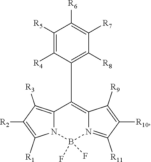
- R 1 , R 2 , R 3 , R 4 , R 5 , R 6 , R 7 , R 8 , R 9 , R 10 , and R 11 are respectively and independently selected from one of a halogen atom, —CN, a tert-butyl group, a non-conjugated structure, and a conjugated structure formed by connecting an alkoxy group with an ester group;
- R 12 , R 13 , R 14 , and R 15 are one of —F, —Cl, Br, —I, —NH 2 , —COOH, —OH, —SH, —COH, —COO—, —COCl, —COBr, —CN, —NO 2 , —NH 2 , ⁇ NH, ⁇ N, a benzene, a phenol ring, an non-conjugated structure, and a conjugated structure formed by connecting an alkoxy group with an ester group, R 16 is an non-conjugated structure, and X ⁇ is one of F ⁇ , Cl ⁇ , Br, CN ⁇ , ClO 4 ⁇ , CF 3 SO 3 ⁇ , CF 2 HSO 3 ⁇ , and CFH 2 SO 3 ⁇ ; and
- the material of the color conversion film further includes a dispersion system, the first compound and the second compound are dispersed in the dispersion system, the dispersion system is a pressure sensitive adhesive, and a mass ratio of the first compound, the second compound, and the dispersion system is (0.4-1.6):(0.3-1.7):(100-1000).
- the conjugated structure formed by the connection of the alkoxy group and the ester group further includes a heterocyclic group
- the heterocyclic group includes one of a five-membered heterocyclic group, a six-membered heterocyclic group, and a benzoheterocyclic group.
- the five-membered heterocyclic group includes one of furan, thiophene, pyrrole, imidazole, and thiazole.
- the six-membered heterocyclic group includes one of pyridine, pyrazine, pyrimidine, and pyridazine.
- the benzoheterocyclic group includes one of indole, quinoline, pteridine, and acridine.
- the present disclosure further provides a color conversion film, and the color conversion film includes the above-mentioned material of the color conversion film.
- the present disclosure further provides a display device, and the display device includes:
- an optical structure including a color conversion film
- a material of the color conversion film includes a first compound and a second compound
- R 1 , R 2 , R 3 , R 4 , R 5 , R 6 , R 7 , R 8 , R 9 , R 10 , and R 11 are respectively and independently selected from one of a halogen atom, —CN, a tert-butyl group, an non-conjugated structure, and a conjugated structure formed by connecting an alkoxy group with an ester group;
- R 12 , R 13 , R 14 , and R 15 are one of —F, —Cl, Br, —I, —NH 2 , —COOH, —OH, —SH, —COH, —COO—, —COCl, —COBr, —CN, —NO 2 , —NH 2 , ⁇ NH, ⁇ N, a benzene, a phenol ring, an non-conjugated structure, and a conjugated structure formed by connecting an alkoxy group with an ester group, R 16 is a non-conjugated structure, and X ⁇ is one of F ⁇ , Cl ⁇ , Br, CN ⁇ , ClO 4 ⁇ , CF 3 SO 3 ⁇ , CF 2 HSO 3 ⁇ , and CFH 2 SO 3 ; and
- the display device further includes a backlight source and a back plate;
- the backlight source is disposed near a lateral side of the optical structure, and the back plate is disposed under a bottom of the optical structure; wherein the optical structure is a light guiding plate, and the color conversion film is disposed at a side of the light guiding plate close to the backlight source; and
- the display device further includes a backlight source and a back plate;
- the backlight source is disposed near a lateral side of the optical structure, and the back plate is disposed under a bottom of the optical structure;
- optical structure is a light guiding plate
- color conversion film is disposed at a lower surface of the light guiding plate close to the back plate
- the light guiding plate further includes a reflective layer
- the reflective layer is disposed at a lower surface of the color conversion film close to the back plate
- the reflective layer includes a plurality of reflective portions
- the display device further includes a barrier layer, and the barrier layer is located near a side of the backlight source away from the baffle.
- FIG. 1 is a sectional view of a first structure of a display device provided by the present disclosure.
- FIG. 2 is a sectional view of a second structure of the display device provided by the present disclosure.
- FIG. 3 is a sectional view of a third structure of the display device provided by the present disclosure.
- FIG. 4 is a sectional view of a fourth structure of the display device provided by the present disclosure.
- R 1 , R 2 , R 3 , R 4 , R 5 , R 6 , R 7 , R 8 , R 9 , R 10 , and R 11 are respectively and independently selected from one of a halogen atom, —CN, a tert-butyl group, a non-conjugated structure, and a conjugated structure formed by connecting an alkoxy group with an ester group.
- a structural formula of the second compound is
- R 12 , R 13 , R 14 , and R 15 are one of —F, —Cl, Br, —I, —NH 2 , —COOH, —OH, —SH, —COH, —COO—, —COCl, —COBr, —CN, —NO 2 , —NH 2 , ⁇ NH, ⁇ N, a benzene, a phenol ring, an non-conjugated structure, and a conjugated structure formed by connecting an alkoxy group with an ester group, and R 10 is an non-conjugated structure.
- the conjugated structure formed by the connection of the alkoxy group and the ester group further includes a heterocyclic group, and the heterocyclic group includes one of a five-membered heterocyclic group, a six-membered heterocyclic group, and a benzoheterocyclic group.
- the five-membered heterocyclic group includes one of furan, thiophene, pyrrole, imidazole, thiazole, and the like.
- the six-membered heterocyclic group includes one of pyridine, pyrazine, pyrimidine, pyridazine, and the like.
- the benzoheterocyclic group includes one of indole, quinoline, pteridine, and acridine.
- X ⁇ is one of F ⁇ , Cl ⁇ , Br, CN ⁇ , ClO 4 ⁇ , CF 3 SO 3 ⁇ , CF 2 HSO 3 ⁇ , and CFH 2 SO 3 ⁇ .
- a mass ratio of the first compound and the second compound is (0.4-1.6):(0.3-1.7). Specifically, the mass ratio of the first compound and the second compound may be one of 0.5:0.6, 0.7:0.9, 1:1, 1:1.2, or 1.4:1.6.
- the R 1 is —Br
- the R 2 is —CN
- the R 3 is —C 2 H 5
- the R 4 is —FC 3 H 6
- the R 5 is —I
- the R 6 is —Cl
- the R 7 is —OC 3 H 7
- the R 8 the R 9 , the R 10 , and the R 11 are the tert-butyl group.
- the structural formula of the first compound may be
- the R 12 is —COOH
- the R 13 is —COH
- the R 14 is —COH
- the R 15 is the benzene
- the X ⁇ is CF 3 SO 3 ⁇ .
- the structural formula of the second compound may be
- the R 12 is —COOH
- the R 13 is —SH
- the R 14 is the phenol ring
- the R 15 is the benzene
- the X ⁇ is ClO 4 ⁇ .
- the structural formula of the second compound may be
- the R 1 is the conjugated structure formed by connecting the alkoxy group with the ester group, for example,
- the R 2 is —CN
- the R 3 is —C 2 H 5
- the R 4 is —FC 3 H 6
- the R 5 is —I
- the R 6 is —Cl
- the R 7 is —OC 3 H 7
- the R 8 the R 9 , the R 10 , and the R 11 are the tert-butyl group.
- the structural formula of the first compound may be
- the R 12 is
- the R 13 is —SH
- R 14 is the phenol ring
- the R 15 is the benzene
- the X ⁇ is ClO 4 ⁇ .
- the structural formula of the first compound may be
- the material of the color conversion film further includes a dispersion system.
- the first compound and the second compound are dispersed in the dispersion system.
- the dispersion system is a pressure sensitive adhesive.
- a mass ratio of the first compound, the second compound, and the dispersion system is (0.4-1.6):(0.3-1.7):(100-1000).
- the dispersion system is the pressure sensitive adhesive.
- the mass ratio of the first compound, the second compound, and the dispersion system may be one of 0.5:0.6:150, 1:1:300, 1:1.2:500, or 1:1:900.
- the dispersion system includes an acrylic resin, an acrylic monomer, and a photoinitiator.
- the first compound and the second compound are dispersed in the dispersion system.
- a mass ratio of the first compound, the second compound, the acrylic resin, the acrylic monomer, and the photoinitiator is (0.4-1.6):(0.3-1.7):(24-300):(74-500):(2-200).
- the mass ratio of the first compound, the second compound, the acrylic resin, the acrylic monomer, and the photoinitiator may be one of 0.5:0.6:30:120:130, 1:1:80:150:160, 1:1.2:50:90:100, or 1:1:25:75:3.
- the material of the color conversion film includes the first compound and the second compound.
- the first compound is a boron fluoride dipyrrole derivative which may absorb cyan light at 480 nm-510 nm, and then emit green light.
- the second compound is a rhodamine 101 derivative which may absorb yellow-orange light at 560 nm-610 nm, and then emit red light.
- the first compound and the second compound are mixed in the dispersion system to form the material of the color conversion film, thus improving a color gamut of the display device.
- the present disclosure further provides a color conversion film.
- the color conversion film is made of the material of the color conversion film which includes all the above-mentioned technical features.
- a color conversion film is provided.
- the first compound is the boron fluoride dipyrrole derivative which may absorb the cyan light at 480 nm-510 nm, and then emit the green light
- the second compound is the rhodamine 101 derivative which may absorb the yellow-orange light at 560 nm-610 nm, and then emit the red light.
- the first compound and the second compound are mixed in the dispersion system to form the material of the color conversion film. Since the first compound, the second compound, and the dispersion system are employed to form the color conversion film, a heat stability of the color conversion film is enhanced, costs of production are reduced, and the color gamut of the display device is improved.
- FIG. 1 is a sectional view of a first structure of a display device provided by the present disclosure.
- the present disclosure provides a display device 10 , and the display device 10 includes an optical structure 20 .
- the optical structure 20 includes a color conversion film 21 .
- the color conversion film includes a first compound and a second compound.
- a structural formula of the first compound is
- R 1 , R 2 , R 3 , R 4 , R 5 , R 6 , R 7 , R 8 , R 9 , R 10 , and R 11 are respectively and independently selected from one of a halogen atom, —CN, a tert-butyl group, a non-conjugated structure, and a conjugated structure formed by connecting an alkoxy group with an ester group.
- a structural formula of the second compound is
- R 12 , R 13 , R 14 , and R 15 are one of —F, —Cl, Br, —I, —NH 2 , —COOH, —OH, —SH, —COH, —COO—, —COCl, —COBr, —CN, —NO 2 , —NH 2 , ⁇ NH, ⁇ N, a benzene, a phenol ring, an non-conjugated structure, and a conjugated structure formed by connecting an alkoxy group with an ester group, R 16 is an non-conjugated structure, and X ⁇ is one of F ⁇ , Cl ⁇ , Br, CN ⁇ , ClO 4 ⁇ , CF 3 SO 3 ⁇ , CF 2 HSO 3 ⁇ , and CFH 2 SO 3 ⁇ .
- a mass ratio of the first compound and the second compound is (0.4-1.6):(0.3-1.7).
- the optical structure may be one of a light
- the display device 10 further includes a backlight source 30 and a back plate 40 .
- the backlight source 30 is disposed near a lateral side of the optical structure 20 .
- the optical structure 20 is the light guiding plate.
- the color conversion film 21 is disposed at a side of the light guiding plate 22 close to the backlight source 30 .
- the back plate 40 is disposed under a bottom of the optical structure 20 .
- the light guiding plate 22 further includes a reflective layer 23 , the reflective layer 23 is disposed at a lower surface of the light guiding plate 22 close to the back plate 40 .
- the reflective layer 23 includes a plurality of reflective portions 231 , and is used to improve a uniformity of light.
- the display device 10 further includes an outer frame 50 , a plastic frame 60 , an aluminum extrusion 70 , a heat dissipation plate 80 , a barrier layer 90 , a fixation structure 100 , a light transmitting layer 110 , and a baffle 120 .
- the outer frame 50 is located near a side of the optical structure 20 close to the backlight source 30 .
- An end of the outer frame 50 close to the backlight source 30 is connected with the plastic frame 60 , thus playing a role of supporting the display device and protecting the structures in the display device from damage.
- Another end of the outer frame 50 away from the backlight source 30 is connected with the back plate 40 .
- the aluminum extrusion 70 is located between the plastic frame 60 and the outer frame 50 .
- the heat dissipation plate 80 is disposed at a surface of the aluminum extrusion 70 close to the optical structure 20 .
- the backlight source 30 is disposed at a surface of the heat dissipation plate 80 close to the optical structure 20 .
- the fixation structure 100 is used to fix the aluminum extrusion 70 to the outer frame 50 .
- the barrier layer 90 is disposed at a surface of the plastic frame 60 close to the backlight source.
- the barrier layer 90 is used to reflect light emitted from the backlight source 30 to the barrier layer 90 , and the reflected light passes through the light transmitting layer 110 and is subsequently emitted to the optical structure 20 .
- the color conversion film 21 is disposed at a surface of the light guiding plate 22 close to the backlight source 30 .
- the light transmitting layer 110 is disposed at a surface of the color conversion film 21 close to the backlight source 30 .
- the baffle 120 is located under a lower surface of the reflective layer 23 close to the back plate 40 .
- the white light emitted by the backlight source passes the color conversion film, the cyan light and the yellow-orange light in the white light are absorbed, so that the light emitted by the backlight source is purified, thus improving the color gamut of the display device.
- FIG. 2 is a sectional view of a second structure of the display device provided by the present disclosure.
- the color conversion film 21 is disposed at a lower surface of the light guiding plate 22 close to the back plate 40 .
- the white light emitted by the backlight source passes the color conversion film, which is disposed at the lower surface of the light guiding plate 22 close to the back plate 40 , as well as the reflective portions 231 , the light is completely reflected in the reflective portions 231 , and the cyan light and the yellow-orange light in the white light are absorbed, so that the red light and the blue light in the backlight source are purified, thus improving the color gamut of the display device.
- the color conversion film 21 is disposed between any two layers of the peeling protection film 200 , the adhesive layer 300 , the passivation layer 400 , the first protection layer 500 , the polarizing sub-layer 600 , the second protection layer 700 , and the surface protection film 800 . Specifically, in the embodiment, the color conversion film 21 is disposed between the passivation layer 400 and the first protection layer 500 .
- the color conversion film is disposed in the polarizer.
- the cyan light and the yellow-orange light in the light are absorbed by the color conversion film in the polarizer, thus purifying the emitted light and improving the color gamut of the display device.
Landscapes
- Chemical & Material Sciences (AREA)
- Physics & Mathematics (AREA)
- Organic Chemistry (AREA)
- Nonlinear Science (AREA)
- Engineering & Computer Science (AREA)
- Materials Engineering (AREA)
- General Physics & Mathematics (AREA)
- Optics & Photonics (AREA)
- Crystallography & Structural Chemistry (AREA)
- Mathematical Physics (AREA)
- Polymers & Plastics (AREA)
- Medicinal Chemistry (AREA)
- Chemical Kinetics & Catalysis (AREA)
- Health & Medical Sciences (AREA)
- Manufacturing & Machinery (AREA)
- Devices For Indicating Variable Information By Combining Individual Elements (AREA)
- Optical Filters (AREA)
- Planar Illumination Modules (AREA)
Abstract
Description

wherein R1, R2, R3, R4, R5, R6, R7, R8, R9, R10, and R11 are respectively and independently selected from one of a halogen atom, —CN, a tert-butyl group, a non-conjugated structure, and a conjugated structure formed by connecting an alkoxy group with an ester group;

wherein R12, R13, R14, and R15 are one of —F, —Cl, Br, —I, —NH2, —COOH, —OH, —SH, —COH, —COO—, —COCl, —COBr, —CN, —NO2, —NH2, ═NH, ≡N, a benzene, a phenol ring, an non-conjugated structure, and a conjugated structure formed by connecting an alkoxy group with an ester group, R16 is an non-conjugated structure, and X− is one of F−, Cl−, Br, CN−, ClO4 −, CF3SO3 −, CF2HSO3 −, and CFH2SO3 −; and

wherein R1, R2, R3, R4, R5, R6, R7, R8, R9, R10, and R11 are respectively and independently selected from one of a halogen atom, —CN, a tert-butyl group, an non-conjugated structure, and a conjugated structure formed by connecting an alkoxy group with an ester group;

wherein R12, R13, R14, and R15 are one of —F, —Cl, Br, —I, —NH2, —COOH, —OH, —SH, —COH, —COO—, —COCl, —COBr, —CN, —NO2, —NH2, ═NH, ≡N, a benzene, a phenol ring, an non-conjugated structure, and a conjugated structure formed by connecting an alkoxy group with an ester group, R16 is a non-conjugated structure, and X− is one of F−, Cl−, Br, CN−, ClO4 −, CF3SO3 −, CF2HSO3 −, and CFH2SO3; and

wherein R1, R2, R3, R4, R5, R6, R7, R8, R9, R10, and R11 are respectively and independently selected from one of a halogen atom, —CN, a tert-butyl group, a non-conjugated structure, and a conjugated structure formed by connecting an alkoxy group with an ester group. A structural formula of the second compound is

wherein R12, R13, R14, and R15 are one of —F, —Cl, Br, —I, —NH2, —COOH, —OH, —SH, —COH, —COO—, —COCl, —COBr, —CN, —NO2, —NH2, ═NH, ≡N, a benzene, a phenol ring, an non-conjugated structure, and a conjugated structure formed by connecting an alkoxy group with an ester group, and R10 is an non-conjugated structure. Specifically, the non-conjugated structure is selected from one of an ester group containing a chain structure, —CnH2n+1, —OCyH2y+1, and —FCmH2m, and n=1-40, y=1-40, and m=1-40. In an embodiment, the conjugated structure formed by the connection of the alkoxy group and the ester group further includes a heterocyclic group, and the heterocyclic group includes one of a five-membered heterocyclic group, a six-membered heterocyclic group, and a benzoheterocyclic group. The five-membered heterocyclic group includes one of furan, thiophene, pyrrole, imidazole, thiazole, and the like. The six-membered heterocyclic group includes one of pyridine, pyrazine, pyrimidine, pyridazine, and the like. The benzoheterocyclic group includes one of indole, quinoline, pteridine, and acridine. X− is one of F−, Cl−, Br, CN−, ClO4 −, CF3SO3 −, CF2HSO3 −, and CFH2SO3 −. A mass ratio of the first compound and the second compound is (0.4-1.6):(0.3-1.7). Specifically, the mass ratio of the first compound and the second compound may be one of 0.5:0.6, 0.7:0.9, 1:1, 1:1.2, or 1.4:1.6.

The R12 is —COOH, the R13 is —COH, the R14 is —COH, the R15 is the benzene, and the R16 is —CnH2n+1, in which when n=1, the R16 is —CH3. The X− is CF3SO3 −. The structural formula of the second compound may be


The R12 is —COOH, the R13 is —SH, the R14 is the phenol ring, the R15 is the benzene, and the R16 is —OCyH2y+1, in which when y=2, the R16 is —OC2H5. The X− is ClO4 −. The structural formula of the second compound may be

The R2 is —CN, the R3 is —C2H5, the R4 is —FC3H6, the R5 is —I, the R6 is —Cl, the R7 is —OC3H7, as well as the R8, the R9, the R10, and the R11 are the tert-butyl group. The structural formula of the first compound may be

The R12 is
the R13 is —SH, R14 is the phenol ring, the R15 is the benzene, and the R16 is —OCyH2y+1, in which when y=1, the R16 is —OC2H5. The X− is ClO4 −. The structural formula of the first compound may be

wherein R1, R2, R3, R4, R5, R6, R7, R8, R9, R10, and R11 are respectively and independently selected from one of a halogen atom, —CN, a tert-butyl group, a non-conjugated structure, and a conjugated structure formed by connecting an alkoxy group with an ester group. A structural formula of the second compound is

wherein R12, R13, R14, and R15 are one of —F, —Cl, Br, —I, —NH2, —COOH, —OH, —SH, —COH, —COO—, —COCl, —COBr, —CN, —NO2, —NH2, ═NH, ≡N, a benzene, a phenol ring, an non-conjugated structure, and a conjugated structure formed by connecting an alkoxy group with an ester group, R16 is an non-conjugated structure, and X− is one of F−, Cl−, Br, CN−, ClO4 −, CF3SO3 −, CF2HSO3 −, and CFH2SO3 −. A mass ratio of the first compound and the second compound is (0.4-1.6):(0.3-1.7). The optical structure may be one of a light guiding plate and a polarizer.
Claims (18)


Applications Claiming Priority (3)
| Application Number | Priority Date | Filing Date | Title |
|---|---|---|---|
| CN202010627149.8 | 2020-07-02 | ||
| CN202010627149.8A CN111849461A (en) | 2020-07-02 | 2020-07-02 | Color conversion film material, color conversion film and display device |
| PCT/CN2020/106700 WO2022000693A1 (en) | 2020-07-02 | 2020-08-04 | Color conversion film material, color conversion film and display device |
Publications (2)
| Publication Number | Publication Date |
|---|---|
| US20220220371A1 US20220220371A1 (en) | 2022-07-14 |
| US11866626B2 true US11866626B2 (en) | 2024-01-09 |
Family
ID=72989045
Family Applications (1)
| Application Number | Title | Priority Date | Filing Date |
|---|---|---|---|
| US17/055,543 Active 2042-05-19 US11866626B2 (en) | 2020-07-02 | 2020-08-04 | Color conversion film material, color conversion film, and display device |
Country Status (3)
| Country | Link |
|---|---|
| US (1) | US11866626B2 (en) |
| CN (1) | CN111849461A (en) |
| WO (1) | WO2022000693A1 (en) |
Families Citing this family (1)
| Publication number | Priority date | Publication date | Assignee | Title |
|---|---|---|---|---|
| JPWO2022130786A1 (en) * | 2020-12-18 | 2022-06-23 |
Citations (10)
| Publication number | Priority date | Publication date | Assignee | Title |
|---|---|---|---|---|
| CN105739167A (en) | 2016-05-06 | 2016-07-06 | 京东方科技集团股份有限公司 | Color film, substrate and display device |
| US20160223728A1 (en) * | 2015-01-31 | 2016-08-04 | Lg Chem, Ltd | Color conversion film and back light unit and display apparatus comprising the same |
| WO2016129298A1 (en) | 2015-02-12 | 2016-08-18 | ソニー株式会社 | Photoelectric conversion film, solid-state imaging element and electronic device |
| CN106154620A (en) | 2014-10-06 | 2016-11-23 | 爱思开哈斯显示用薄膜有限公司 | Excitation reinforcing membrane and include the liquid crystal indicator of this film |
| CN109073933A (en) | 2016-04-18 | 2018-12-21 | 株式会社Lg化学 | Color conversion film, and backlight unit and display device including the same |
| CN109768181A (en) | 2019-01-18 | 2019-05-17 | 深圳市华星光电技术有限公司 | White organic LED display device and its manufacturing method |
| US20190367735A1 (en) | 2018-05-29 | 2019-12-05 | Elitechgroup, Inc. | Carborhodamine compounds and methods of preparation thereof |
| WO2019243288A1 (en) | 2018-06-22 | 2019-12-26 | Basf Se | Extruded pet films with photostable dyes for color conversion |
| CN110808322A (en) | 2019-10-14 | 2020-02-18 | 深圳市华星光电技术有限公司 | LED white light device and backlight module |
| CN111077698A (en) * | 2019-12-17 | 2020-04-28 | Tcl华星光电技术有限公司 | Backlight module and liquid crystal display device |
-
2020
- 2020-07-02 CN CN202010627149.8A patent/CN111849461A/en active Pending
- 2020-08-04 US US17/055,543 patent/US11866626B2/en active Active
- 2020-08-04 WO PCT/CN2020/106700 patent/WO2022000693A1/en not_active Ceased
Patent Citations (11)
| Publication number | Priority date | Publication date | Assignee | Title |
|---|---|---|---|---|
| CN106154620A (en) | 2014-10-06 | 2016-11-23 | 爱思开哈斯显示用薄膜有限公司 | Excitation reinforcing membrane and include the liquid crystal indicator of this film |
| US20160223728A1 (en) * | 2015-01-31 | 2016-08-04 | Lg Chem, Ltd | Color conversion film and back light unit and display apparatus comprising the same |
| WO2016129298A1 (en) | 2015-02-12 | 2016-08-18 | ソニー株式会社 | Photoelectric conversion film, solid-state imaging element and electronic device |
| CN109073933A (en) | 2016-04-18 | 2018-12-21 | 株式会社Lg化学 | Color conversion film, and backlight unit and display device including the same |
| CN105739167A (en) | 2016-05-06 | 2016-07-06 | 京东方科技集团股份有限公司 | Color film, substrate and display device |
| US20190367735A1 (en) | 2018-05-29 | 2019-12-05 | Elitechgroup, Inc. | Carborhodamine compounds and methods of preparation thereof |
| WO2019243288A1 (en) | 2018-06-22 | 2019-12-26 | Basf Se | Extruded pet films with photostable dyes for color conversion |
| TW202000864A (en) | 2018-06-22 | 2020-01-01 | 德商巴地斯顏料化工廠 | Extruded PET films with photostable dyes for color conversion |
| CN109768181A (en) | 2019-01-18 | 2019-05-17 | 深圳市华星光电技术有限公司 | White organic LED display device and its manufacturing method |
| CN110808322A (en) | 2019-10-14 | 2020-02-18 | 深圳市华星光电技术有限公司 | LED white light device and backlight module |
| CN111077698A (en) * | 2019-12-17 | 2020-04-28 | Tcl华星光电技术有限公司 | Backlight module and liquid crystal display device |
Also Published As
| Publication number | Publication date |
|---|---|
| US20220220371A1 (en) | 2022-07-14 |
| WO2022000693A1 (en) | 2022-01-06 |
| CN111849461A (en) | 2020-10-30 |
Similar Documents
| Publication | Publication Date | Title |
|---|---|---|
| US10501688B2 (en) | Enhanced wavelength converting structure | |
| US10988619B2 (en) | Manufacturing method of rhodamine dye oligomer, solid color material and liquid crystal display device | |
| CN101788132B (en) | Optical member and display device | |
| WO2016011691A1 (en) | High-color-gamut liquid crystal display module structure | |
| CN110730927B (en) | Display device | |
| TW200745694A (en) | Liquid crystal panel and liquid crystal display device | |
| US11846848B2 (en) | Backlight assembly and display apparatus | |
| US11866626B2 (en) | Color conversion film material, color conversion film, and display device | |
| TWI267681B (en) | Liquid crystal display | |
| JP2003066451A (en) | Liquid crystal display | |
| WO2013182018A1 (en) | Black projection screen | |
| US11249231B2 (en) | Optical purification layer, edge-lit backlight module and polarizer | |
| TWI399585B (en) | Liquid crystal display panel and color filter substrate | |
| CN110361806B (en) | Iodine-based polarizing plate and display device | |
| WO2020228191A1 (en) | Preparation method for dye and optical film | |
| US20150362785A1 (en) | Display device | |
| US20210111314A1 (en) | Led white light device and backlight module | |
| WO2018194019A1 (en) | Liquid crystal panel and liquid crystal display device | |
| CN110058449B (en) | Quantum dot liquid crystal display | |
| US10809565B2 (en) | Backlight module and display device | |
| US11335736B2 (en) | White OLED display device and method of manufacturing same | |
| CN107748405B (en) | Color filter and backlight module | |
| JP4776051B2 (en) | Liquid crystal display | |
| CN112226099A (en) | An organic dye, backlight module, polarizer and display panel | |
| TWM392978U (en) | Backlight module and liquid crystal display |
Legal Events
| Date | Code | Title | Description |
|---|---|---|---|
| FEPP | Fee payment procedure |
Free format text: ENTITY STATUS SET TO UNDISCOUNTED (ORIGINAL EVENT CODE: BIG.); ENTITY STATUS OF PATENT OWNER: LARGE ENTITY |
|
| AS | Assignment |
Owner name: TCL CHINA STAR OPTOELECTRONICS TECHNOLOGY CO., LTD., CHINA Free format text: ASSIGNMENT OF ASSIGNORS INTEREST;ASSIGNOR:ZHA, BAO;REEL/FRAME:054369/0377 Effective date: 20201027 |
|
| STPP | Information on status: patent application and granting procedure in general |
Free format text: DOCKETED NEW CASE - READY FOR EXAMINATION |
|
| STPP | Information on status: patent application and granting procedure in general |
Free format text: NOTICE OF ALLOWANCE MAILED -- APPLICATION RECEIVED IN OFFICE OF PUBLICATIONS |
|
| STPP | Information on status: patent application and granting procedure in general |
Free format text: PUBLICATIONS -- ISSUE FEE PAYMENT RECEIVED |
|
| STPP | Information on status: patent application and granting procedure in general |
Free format text: PUBLICATIONS -- ISSUE FEE PAYMENT VERIFIED |
|
| STCF | Information on status: patent grant |
Free format text: PATENTED CASE |