US11830784B2 - Leadframe spacer for double-sided power module - Google Patents
Leadframe spacer for double-sided power module Download PDFInfo
- Publication number
- US11830784B2 US11830784B2 US17/447,011 US202117447011A US11830784B2 US 11830784 B2 US11830784 B2 US 11830784B2 US 202117447011 A US202117447011 A US 202117447011A US 11830784 B2 US11830784 B2 US 11830784B2
- Authority
- US
- United States
- Prior art keywords
- semiconductor device
- leadframe
- spacer
- substrate
- downset
- Prior art date
- Legal status (The legal status is an assumption and is not a legal conclusion. Google has not performed a legal analysis and makes no representation as to the accuracy of the status listed.)
- Active, expires
Links
Images


Classifications
-
- H—ELECTRICITY
- H10—SEMICONDUCTOR DEVICES; ELECTRIC SOLID-STATE DEVICES NOT OTHERWISE PROVIDED FOR
- H10W—GENERIC PACKAGES, INTERCONNECTIONS, CONNECTORS OR OTHER CONSTRUCTIONAL DETAILS OF DEVICES COVERED BY CLASS H10
- H10W70/00—Package substrates; Interposers; Redistribution layers [RDL]
- H10W70/40—Leadframes
- H10W70/461—Leadframes specially adapted for cooling
-
- H01L23/3675—
-
- H—ELECTRICITY
- H10—SEMICONDUCTOR DEVICES; ELECTRIC SOLID-STATE DEVICES NOT OTHERWISE PROVIDED FOR
- H10W—GENERIC PACKAGES, INTERCONNECTIONS, CONNECTORS OR OTHER CONSTRUCTIONAL DETAILS OF DEVICES COVERED BY CLASS H10
- H10W40/00—Arrangements for thermal protection or thermal control
- H10W40/20—Arrangements for cooling
- H10W40/22—Arrangements for cooling characterised by their shape, e.g. having conical or cylindrical projections
-
- H01L21/52—
-
- H01L21/565—
-
- H01L23/3735—
-
- H01L23/49575—
-
- H01L24/32—
-
- H01L24/33—
-
- H—ELECTRICITY
- H05—ELECTRIC TECHNIQUES NOT OTHERWISE PROVIDED FOR
- H05K—PRINTED CIRCUITS; CASINGS OR CONSTRUCTIONAL DETAILS OF ELECTRIC APPARATUS; MANUFACTURE OF ASSEMBLAGES OF ELECTRICAL COMPONENTS
- H05K7/00—Constructional details common to different types of electric apparatus
- H05K7/20—Modifications to facilitate cooling, ventilating, or heating
- H05K7/2089—Modifications to facilitate cooling, ventilating, or heating for power electronics, e.g. for inverters for controlling motor
-
- H—ELECTRICITY
- H10—SEMICONDUCTOR DEVICES; ELECTRIC SOLID-STATE DEVICES NOT OTHERWISE PROVIDED FOR
- H10W—GENERIC PACKAGES, INTERCONNECTIONS, CONNECTORS OR OTHER CONSTRUCTIONAL DETAILS OF DEVICES COVERED BY CLASS H10
- H10W40/00—Arrangements for thermal protection or thermal control
- H10W40/20—Arrangements for cooling
- H10W40/25—Arrangements for cooling characterised by their materials
- H10W40/255—Arrangements for cooling characterised by their materials having a laminate or multilayered structure, e.g. direct bond copper [DBC] ceramic substrates
-
- H—ELECTRICITY
- H10—SEMICONDUCTOR DEVICES; ELECTRIC SOLID-STATE DEVICES NOT OTHERWISE PROVIDED FOR
- H10W—GENERIC PACKAGES, INTERCONNECTIONS, CONNECTORS OR OTHER CONSTRUCTIONAL DETAILS OF DEVICES COVERED BY CLASS H10
- H10W40/00—Arrangements for thermal protection or thermal control
- H10W40/70—Fillings or auxiliary members in containers or in encapsulations for thermal protection or control
- H10W40/77—Auxiliary members characterised by their shape
- H10W40/778—Auxiliary members characterised by their shape in encapsulations
-
- H—ELECTRICITY
- H10—SEMICONDUCTOR DEVICES; ELECTRIC SOLID-STATE DEVICES NOT OTHERWISE PROVIDED FOR
- H10W—GENERIC PACKAGES, INTERCONNECTIONS, CONNECTORS OR OTHER CONSTRUCTIONAL DETAILS OF DEVICES COVERED BY CLASS H10
- H10W70/00—Package substrates; Interposers; Redistribution layers [RDL]
- H10W70/40—Leadframes
- H10W70/464—Additional interconnections in combination with leadframes
- H10W70/468—Circuit boards
-
- H—ELECTRICITY
- H10—SEMICONDUCTOR DEVICES; ELECTRIC SOLID-STATE DEVICES NOT OTHERWISE PROVIDED FOR
- H10W—GENERIC PACKAGES, INTERCONNECTIONS, CONNECTORS OR OTHER CONSTRUCTIONAL DETAILS OF DEVICES COVERED BY CLASS H10
- H10W72/00—Interconnections or connectors in packages
- H10W72/071—Connecting or disconnecting
-
- H—ELECTRICITY
- H10—SEMICONDUCTOR DEVICES; ELECTRIC SOLID-STATE DEVICES NOT OTHERWISE PROVIDED FOR
- H10W—GENERIC PACKAGES, INTERCONNECTIONS, CONNECTORS OR OTHER CONSTRUCTIONAL DETAILS OF DEVICES COVERED BY CLASS H10
- H10W72/00—Interconnections or connectors in packages
- H10W72/30—Die-attach connectors
-
- H—ELECTRICITY
- H10—SEMICONDUCTOR DEVICES; ELECTRIC SOLID-STATE DEVICES NOT OTHERWISE PROVIDED FOR
- H10W—GENERIC PACKAGES, INTERCONNECTIONS, CONNECTORS OR OTHER CONSTRUCTIONAL DETAILS OF DEVICES COVERED BY CLASS H10
- H10W74/00—Encapsulations, e.g. protective coatings
- H10W74/01—Manufacture or treatment
- H10W74/016—Manufacture or treatment using moulds
-
- H—ELECTRICITY
- H10—SEMICONDUCTOR DEVICES; ELECTRIC SOLID-STATE DEVICES NOT OTHERWISE PROVIDED FOR
- H10W—GENERIC PACKAGES, INTERCONNECTIONS, CONNECTORS OR OTHER CONSTRUCTIONAL DETAILS OF DEVICES COVERED BY CLASS H10
- H10W76/00—Containers; Fillings or auxiliary members therefor; Seals
- H10W76/10—Containers or parts thereof
- H10W76/12—Containers or parts thereof characterised by their shape
- H10W76/13—Containers comprising a conductive base serving as an interconnection
- H10W76/136—Containers comprising a conductive base serving as an interconnection having other interconnections perpendicular to the conductive base
-
- H—ELECTRICITY
- H10—SEMICONDUCTOR DEVICES; ELECTRIC SOLID-STATE DEVICES NOT OTHERWISE PROVIDED FOR
- H10W—GENERIC PACKAGES, INTERCONNECTIONS, CONNECTORS OR OTHER CONSTRUCTIONAL DETAILS OF DEVICES COVERED BY CLASS H10
- H10W90/00—Package configurations
-
- H—ELECTRICITY
- H10—SEMICONDUCTOR DEVICES; ELECTRIC SOLID-STATE DEVICES NOT OTHERWISE PROVIDED FOR
- H10W—GENERIC PACKAGES, INTERCONNECTIONS, CONNECTORS OR OTHER CONSTRUCTIONAL DETAILS OF DEVICES COVERED BY CLASS H10
- H10W90/00—Package configurations
- H10W90/811—Multiple chips on leadframes
-
- H—ELECTRICITY
- H10—SEMICONDUCTOR DEVICES; ELECTRIC SOLID-STATE DEVICES NOT OTHERWISE PROVIDED FOR
- H10W—GENERIC PACKAGES, INTERCONNECTIONS, CONNECTORS OR OTHER CONSTRUCTIONAL DETAILS OF DEVICES COVERED BY CLASS H10
- H10W95/00—Packaging processes not covered by the other groups of this subclass
-
- H01L2224/32245—
-
- H01L2224/40245—
-
- H01L2224/84801—
-
- H01L23/49524—
-
- H01L23/49551—
-
- H01L23/49562—
-
- H01L2924/13055—
-
- H—ELECTRICITY
- H10—SEMICONDUCTOR DEVICES; ELECTRIC SOLID-STATE DEVICES NOT OTHERWISE PROVIDED FOR
- H10W—GENERIC PACKAGES, INTERCONNECTIONS, CONNECTORS OR OTHER CONSTRUCTIONAL DETAILS OF DEVICES COVERED BY CLASS H10
- H10W70/00—Package substrates; Interposers; Redistribution layers [RDL]
- H10W70/40—Leadframes
- H10W70/421—Shapes or dispositions
- H10W70/424—Cross-sectional shapes
- H10W70/427—Bent parts
-
- H—ELECTRICITY
- H10—SEMICONDUCTOR DEVICES; ELECTRIC SOLID-STATE DEVICES NOT OTHERWISE PROVIDED FOR
- H10W—GENERIC PACKAGES, INTERCONNECTIONS, CONNECTORS OR OTHER CONSTRUCTIONAL DETAILS OF DEVICES COVERED BY CLASS H10
- H10W70/00—Package substrates; Interposers; Redistribution layers [RDL]
- H10W70/40—Leadframes
- H10W70/464—Additional interconnections in combination with leadframes
- H10W70/466—Tape carriers or flat leads
-
- H—ELECTRICITY
- H10—SEMICONDUCTOR DEVICES; ELECTRIC SOLID-STATE DEVICES NOT OTHERWISE PROVIDED FOR
- H10W—GENERIC PACKAGES, INTERCONNECTIONS, CONNECTORS OR OTHER CONSTRUCTIONAL DETAILS OF DEVICES COVERED BY CLASS H10
- H10W70/00—Package substrates; Interposers; Redistribution layers [RDL]
- H10W70/40—Leadframes
- H10W70/481—Leadframes for devices being provided for in groups H10D8/00 - H10D48/00
-
- H—ELECTRICITY
- H10—SEMICONDUCTOR DEVICES; ELECTRIC SOLID-STATE DEVICES NOT OTHERWISE PROVIDED FOR
- H10W—GENERIC PACKAGES, INTERCONNECTIONS, CONNECTORS OR OTHER CONSTRUCTIONAL DETAILS OF DEVICES COVERED BY CLASS H10
- H10W70/00—Package substrates; Interposers; Redistribution layers [RDL]
- H10W70/60—Insulating or insulated package substrates; Interposers; Redistribution layers
- H10W70/67—Insulating or insulated package substrates; Interposers; Redistribution layers characterised by their insulating layers or insulating parts
- H10W70/68—Shapes or dispositions thereof
- H10W70/682—Shapes or dispositions thereof comprising holes having chips therein
-
- H—ELECTRICITY
- H10—SEMICONDUCTOR DEVICES; ELECTRIC SOLID-STATE DEVICES NOT OTHERWISE PROVIDED FOR
- H10W—GENERIC PACKAGES, INTERCONNECTIONS, CONNECTORS OR OTHER CONSTRUCTIONAL DETAILS OF DEVICES COVERED BY CLASS H10
- H10W72/00—Interconnections or connectors in packages
- H10W72/071—Connecting or disconnecting
- H10W72/073—Connecting or disconnecting of die-attach connectors
- H10W72/07331—Connecting techniques
- H10W72/07336—Soldering or alloying
-
- H—ELECTRICITY
- H10—SEMICONDUCTOR DEVICES; ELECTRIC SOLID-STATE DEVICES NOT OTHERWISE PROVIDED FOR
- H10W—GENERIC PACKAGES, INTERCONNECTIONS, CONNECTORS OR OTHER CONSTRUCTIONAL DETAILS OF DEVICES COVERED BY CLASS H10
- H10W72/00—Interconnections or connectors in packages
- H10W72/071—Connecting or disconnecting
- H10W72/073—Connecting or disconnecting of die-attach connectors
- H10W72/07351—Connecting or disconnecting of die-attach connectors characterised by changes in properties of the die-attach connectors during connecting
- H10W72/07352—Connecting or disconnecting of die-attach connectors characterised by changes in properties of the die-attach connectors during connecting changes in structures or sizes
-
- H—ELECTRICITY
- H10—SEMICONDUCTOR DEVICES; ELECTRIC SOLID-STATE DEVICES NOT OTHERWISE PROVIDED FOR
- H10W—GENERIC PACKAGES, INTERCONNECTIONS, CONNECTORS OR OTHER CONSTRUCTIONAL DETAILS OF DEVICES COVERED BY CLASS H10
- H10W72/00—Interconnections or connectors in packages
- H10W72/071—Connecting or disconnecting
- H10W72/073—Connecting or disconnecting of die-attach connectors
- H10W72/07351—Connecting or disconnecting of die-attach connectors characterised by changes in properties of the die-attach connectors during connecting
- H10W72/07354—Connecting or disconnecting of die-attach connectors characterised by changes in properties of the die-attach connectors during connecting changes in dispositions
-
- H—ELECTRICITY
- H10—SEMICONDUCTOR DEVICES; ELECTRIC SOLID-STATE DEVICES NOT OTHERWISE PROVIDED FOR
- H10W—GENERIC PACKAGES, INTERCONNECTIONS, CONNECTORS OR OTHER CONSTRUCTIONAL DETAILS OF DEVICES COVERED BY CLASS H10
- H10W72/00—Interconnections or connectors in packages
- H10W72/071—Connecting or disconnecting
- H10W72/076—Connecting or disconnecting of strap connectors
- H10W72/07631—Techniques
- H10W72/07636—Soldering or alloying
-
- H—ELECTRICITY
- H10—SEMICONDUCTOR DEVICES; ELECTRIC SOLID-STATE DEVICES NOT OTHERWISE PROVIDED FOR
- H10W—GENERIC PACKAGES, INTERCONNECTIONS, CONNECTORS OR OTHER CONSTRUCTIONAL DETAILS OF DEVICES COVERED BY CLASS H10
- H10W72/00—Interconnections or connectors in packages
- H10W72/20—Bump connectors, e.g. solder bumps or copper pillars; Dummy bumps; Thermal bumps
-
- H—ELECTRICITY
- H10—SEMICONDUCTOR DEVICES; ELECTRIC SOLID-STATE DEVICES NOT OTHERWISE PROVIDED FOR
- H10W—GENERIC PACKAGES, INTERCONNECTIONS, CONNECTORS OR OTHER CONSTRUCTIONAL DETAILS OF DEVICES COVERED BY CLASS H10
- H10W72/00—Interconnections or connectors in packages
- H10W72/30—Die-attach connectors
- H10W72/321—Structures or relative sizes of die-attach connectors
- H10W72/327—Multiple die-attach connectors having different sizes
-
- H—ELECTRICITY
- H10—SEMICONDUCTOR DEVICES; ELECTRIC SOLID-STATE DEVICES NOT OTHERWISE PROVIDED FOR
- H10W—GENERIC PACKAGES, INTERCONNECTIONS, CONNECTORS OR OTHER CONSTRUCTIONAL DETAILS OF DEVICES COVERED BY CLASS H10
- H10W72/00—Interconnections or connectors in packages
- H10W72/30—Die-attach connectors
- H10W72/341—Dispositions of die-attach connectors, e.g. layouts
- H10W72/347—Dispositions of multiple die-attach connectors
-
- H—ELECTRICITY
- H10—SEMICONDUCTOR DEVICES; ELECTRIC SOLID-STATE DEVICES NOT OTHERWISE PROVIDED FOR
- H10W—GENERIC PACKAGES, INTERCONNECTIONS, CONNECTORS OR OTHER CONSTRUCTIONAL DETAILS OF DEVICES COVERED BY CLASS H10
- H10W72/00—Interconnections or connectors in packages
- H10W72/30—Die-attach connectors
- H10W72/351—Materials of die-attach connectors
- H10W72/352—Materials of die-attach connectors comprising metals or metalloids, e.g. solders
-
- H—ELECTRICITY
- H10—SEMICONDUCTOR DEVICES; ELECTRIC SOLID-STATE DEVICES NOT OTHERWISE PROVIDED FOR
- H10W—GENERIC PACKAGES, INTERCONNECTIONS, CONNECTORS OR OTHER CONSTRUCTIONAL DETAILS OF DEVICES COVERED BY CLASS H10
- H10W72/00—Interconnections or connectors in packages
- H10W72/50—Bond wires
- H10W72/59—Bond pads specially adapted therefor
-
- H—ELECTRICITY
- H10—SEMICONDUCTOR DEVICES; ELECTRIC SOLID-STATE DEVICES NOT OTHERWISE PROVIDED FOR
- H10W—GENERIC PACKAGES, INTERCONNECTIONS, CONNECTORS OR OTHER CONSTRUCTIONAL DETAILS OF DEVICES COVERED BY CLASS H10
- H10W72/00—Interconnections or connectors in packages
- H10W72/90—Bond pads, in general
- H10W72/921—Structures or relative sizes of bond pads
- H10W72/926—Multiple bond pads having different sizes
-
- H—ELECTRICITY
- H10—SEMICONDUCTOR DEVICES; ELECTRIC SOLID-STATE DEVICES NOT OTHERWISE PROVIDED FOR
- H10W—GENERIC PACKAGES, INTERCONNECTIONS, CONNECTORS OR OTHER CONSTRUCTIONAL DETAILS OF DEVICES COVERED BY CLASS H10
- H10W74/00—Encapsulations, e.g. protective coatings
-
- H—ELECTRICITY
- H10—SEMICONDUCTOR DEVICES; ELECTRIC SOLID-STATE DEVICES NOT OTHERWISE PROVIDED FOR
- H10W—GENERIC PACKAGES, INTERCONNECTIONS, CONNECTORS OR OTHER CONSTRUCTIONAL DETAILS OF DEVICES COVERED BY CLASS H10
- H10W90/00—Package configurations
- H10W90/701—Package configurations characterised by the relative positions of pads or connectors relative to package parts
- H10W90/731—Package configurations characterised by the relative positions of pads or connectors relative to package parts of die-attach connectors
- H10W90/734—Package configurations characterised by the relative positions of pads or connectors relative to package parts of die-attach connectors between a chip and a stacked insulating package substrate, interposer or RDL
-
- H—ELECTRICITY
- H10—SEMICONDUCTOR DEVICES; ELECTRIC SOLID-STATE DEVICES NOT OTHERWISE PROVIDED FOR
- H10W—GENERIC PACKAGES, INTERCONNECTIONS, CONNECTORS OR OTHER CONSTRUCTIONAL DETAILS OF DEVICES COVERED BY CLASS H10
- H10W90/00—Package configurations
- H10W90/701—Package configurations characterised by the relative positions of pads or connectors relative to package parts
- H10W90/731—Package configurations characterised by the relative positions of pads or connectors relative to package parts of die-attach connectors
- H10W90/736—Package configurations characterised by the relative positions of pads or connectors relative to package parts of die-attach connectors between a chip and a stacked lead frame, conducting package substrate or heat sink
-
- H—ELECTRICITY
- H10—SEMICONDUCTOR DEVICES; ELECTRIC SOLID-STATE DEVICES NOT OTHERWISE PROVIDED FOR
- H10W—GENERIC PACKAGES, INTERCONNECTIONS, CONNECTORS OR OTHER CONSTRUCTIONAL DETAILS OF DEVICES COVERED BY CLASS H10
- H10W90/00—Package configurations
- H10W90/701—Package configurations characterised by the relative positions of pads or connectors relative to package parts
- H10W90/761—Package configurations characterised by the relative positions of pads or connectors relative to package parts of strap connectors
- H10W90/766—Package configurations characterised by the relative positions of pads or connectors relative to package parts of strap connectors between a chip and a stacked lead frame, conducting package substrate or heat sink
Definitions
- This description relates to semiconductor packaging techniques for power modules.
- IGBT Insulated Gate Bipolar Transistor
- FPD Fast Recovery Diode
- Such semiconductor devices are packaged to enable connections with other circuits, and to deploy the semiconductor devices in a manner that is space-efficient and reliable.
- Semiconductor devices packaged within a power module may have high demands in terms of electrical, mechanical, and thermal reliability.
- a semiconductor device module includes a first substrate, and a leadframe spacer having a first side electrically connected to the first substrate and including at least one downset defining a recess that provides a die attach pad (DAP) on a second side of the leadframe spacer that is opposite the first side.
- the semiconductor device module includes a first semiconductor device disposed within the recess and electrically connected to the DAP, a second semiconductor device disposed within the recess and electrically connected to the DAP, and a second substrate mounted on the second side of the leadframe spacer on at least one downset surface of the at least one downset and at least partially enclosing the first semiconductor device and the second semiconductor device within the recess.
- a semiconductor device module includes a leadframe spacer having a first side and a second side, the second side having at least one downset with at least one downset surface, a first substrate mounted to the first side of the leadframe spacer, and a second substrate mounted to the at least one downset surface.
- the semiconductor device module includes a first semiconductor device electrically connected to the second side of the leadframe spacer and to the second substrate, and a second semiconductor device electrically connected to the second side of the leadframe spacer and to the second substrate.
- a method of manufacturing a semiconductor device module includes mounting a first substrate to a first side of a leadframe spacer, the leadframe spacer including at least one downset defining a recess that provides a die attach pad (DAP) on a second side of the leadframe spacer that is opposite the first side.
- the method further includes mounting a first semiconductor device and a second semiconductor device onto the DAP, and mounting a second substrate on the second side of the leadframe spacer on at least one downset surface of the at least one downset and at least partially enclosing the first semiconductor device and the second semiconductor device within the recess.
- DAP die attach pad
- FIG. 1 is a simplified, partially exploded view of a leadframe spacer for a double-sided cooling power module.
- FIG. 2 is a cross-section of an example implementation of a double-sided cooling power module using the leadframe spacer of FIG. 1 .
- FIG. 3 is a cross-section of a first example process step for forming the example implementation of FIG. 2 .
- FIG. 4 is a cross-section of a second example process step for forming the example implementation of FIG. 2 .
- FIG. 5 is a cross-section of a third example process step for forming the example implementation of FIG. 2 .
- FIG. 6 is a cross-section of a fourth example process step for forming the example implementation of FIG. 2 .
- FIG. 7 is a flowchart illustrating example process steps corresponding to the examples of FIGS. 3 - 6 .
- FIG. 8 is an exploded view of a more detailed example implementation of a double-sided power module with a leadframe spacer, corresponding to the example of FIG. 1 .
- FIG. 9 is a top view of the leadframe spacer of FIG. 8 .
- FIG. 10 is a side-angle view of the leadframe spacer of FIG. 8 .
- FIG. 11 is a top view of an assembled version of the example of FIG. 8 , prior to molding.
- FIG. 12 is a top view of an assembled version of the example of FIG. 8 , with molding completed.
- FIG. 13 is a transparent top view of the example of FIG. 12 .
- FIG. 14 is a cross-section of FIG. 13 taken at line A-A.
- FIG. 15 is a cross-section of FIG. 13 taken at line B-B.
- FIG. 16 is a graph illustrating peeling strain levels at solder joints of signal pads, in example embodiments.
- FIG. 17 is a graph illustrating thermal resistance levels, in example embodiments.
- a leadframe spacer provides the functions of both a leadframe and a spacer of conventional power modules, while also enabling a double-sided cooling configuration.
- such a leadframe spacer may include a leadframe surface that provides a die attach pad (DAP) that is shared by (and electrically connected to) at least two semiconductor devices, such as an IGBT and a diode.
- the leadframe spacer may include at least one downset, which provides one or more downset surfaces and defines a recess, and where the semiconductor devices are attached within the recess.
- a first substrate may be connected to a first side of the leadframe (opposite the semiconductor devices), and a second substrate may be connected to the downset surfaces, and thereby positioned for further connection to the semiconductor devices in a double-sided, dual, or flip chip assembly.
- a leadframe may be used to provide electrical connections outside of the power module, and the spacers may be used to provide mechanical support and desired positioning for each semiconductor device, relative to a first substrate (e.g., a direct bond copper (DBC) substrate).
- a first substrate e.g., a direct bond copper (DBC) substrate.
- DBC direct bond copper
- separate spacers may be used for each of an IGBT and a diode.
- CTE coefficients of thermal expansion
- EMC Epoxy Molding Compound
- the designs described herein replace conventional, discrete spacers with a single, low-cost leadframe spacer.
- the leadframe spacer may be made of a single piece of metal that may be easily handled and used during an assembly process.
- the described leadframe spacer provides improved mechanical reliability, including reducing (e.g., sharing) an effect of the thermal stress/strain, and reducing peeling (e.g., at solder joints of signal pads).
- the described leadframe spacer includes a surface within a recess that provides a DAP shared by at least two semiconductor devices, and the shared DAP further provides improved thermal resistance, reduced electrical parasitics, low thermal/electrical resistance, and low electrical inductance, thereby resulting in higher power capability.
- the recess is formed by at least one downset, e.g., at least two downsets, which further contribute to the above-referenced reductions in peeling and other negative effects of thermal and mechanical stress/strain. Additionally, the downsets provide downset surfaces such that the leadframe spacer may be electrically and mechanically connected to both substrates of a double-sided power module, and the semiconductor devices enclosed within the recess may easily and reliably be connected to external circuit elements in a desired manner.
- FIG. 1 is a simplified, partially exploded view of a leadframe spacer 102 for a double-sided power module.
- the leadframe spacer 102 is used to mount a first semiconductor device 104 (e.g., an IGBT) and a second semiconductor device 106 (e.g., a diode).
- a first substrate 108 is positioned for mounting to a first side of the leadframe spacer 102
- a second substrate 110 is positioned for mounting to a second, opposing side of the leadframe spacer 102 .
- the first substrate 108 is positioned for mounting to a planar surface 112 of the leadframe spacer 102 , on a first side of the leadframe spacer 102 .
- the leadframe spacer 102 includes at least two downsets 114 , which define a Die Attach Pad (DAP) surface 115 , on which the semiconductor devices 104 , 106 may be mounted.
- DAP Die Attach Pad
- the leadframe 102 includes downset surfaces 116 , so that a recess 117 is formed between the downset surfaces 116 and the DAP 115 .
- the second substrate 110 may thus be mounted to the downset surfaces 116 , in a plane that enables desired connections of the second substrate 110 to the semiconductor devices 104 , 106 .
- Example downset(s) 114 may include any portion of the leadframe spacer 102 that define a spatial offset between the DAP surface 115 and the downset surfaces 116 that is sufficient to position the semiconductor devices 104 , 106 on the DAP surface 115 , while mounting the second substrate 110 using the downset surfaces 116 . Put another way, the downset(s) 114 define a displacement in a direction perpendicular to the DAP surface 115 .
- the downset(s) 114 may be perpendicular to the DAP surface 115 , or may be angled relative to the DAP surface 115 , or combinations thereof. As illustrated in more detail, below, e.g., in the examples of FIGS. 8 - 15 , the downset(s) 114 may extend at least partially around a perimeter or other portion of the leadframe spacer 102 .
- the downset surfaces 116 may extend in a direction parallel to the DAP surface 115 , and perpendicular to the downsets 114 .
- An angled portion 118 may be connected to the downset surface 116 and to a lead 120 , to thereby provide additional force absorption and mechanical strain relief.
- the downsets 114 may be angled relative to the DAP surface 115 , as long as a depth of the recess 117 is sufficient to include the semiconductor devices 104 , 106 within the recess 117 . Accordingly, the semiconductor devices 104 , 106 may be at least partially enclosed within the recess 117 by the attaching of the second substrate 110 to the downset surfaces 116 .
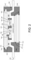
- FIG. 2 is a cross-section of an example implementation of a double-sided power module using the leadframe spacer of FIG. 1 .
- FIG. 2 illustrates an assembled version of FIG. 1 , including more specific example implementation details, including solder connections.
- a leadframe spacer 202 is used to mount IGBT 204 and diode 206 , within a downset-defined recess of the leadframe spacer 202 , and otherwise in the manner described above with respect to FIG. 1 .
- a first substrate 208 is mounted to a first side of the leadframe spacer 202 (opposite the IGBT 204 and the diode 206 ).
- a second substrate 210 is mounted on the second, opposing (device-side) side of the leadframe spacer 202 , using downset surfaces of the leadframe spacer 202 .
- the first substrate 208 is a DBC substrate that includes a first copper layer 212 , a dielectric layer 214 (e.g., a ceramic layer, such as Al 2 O 3 ), and a second copper layer 216 .
- the second substrate 210 is a DBC substrate that includes a first copper layer 218 , a dielectric layer 220 (e.g., a ceramic layer, such as Al 2 O 3 ), and a second copper layer 222 / 223 that includes a first portion 222 , and a second portion 223 , as illustrated and as described in more detail, below.
- Solder connections are illustrated in FIG. 2 , including a solder layer 224 connecting the first substrate 208 to the leadframe spacer 202 , a solder layer 226 connecting the IGBT 204 to the leadframe spacer 202 , and a solder layer 228 connecting the diode 206 to the leadframe spacer 202 .
- the second substrate 210 has the portion 222 connected by solder layer 230 to a downset surface of the leadframe spacer 202 , and the portion 223 connected by solder layer 232 to a downset surface of the leadframe spacer 202 .
- the portion 223 is further connected by solder layer 234 to the IGBT 204 , and by solder layer 236 to the diode 206 .
- the portion 222 is further connected by solder layer 238 to the IGBT (e.g., to a gate of the IGBT).
- molding 240 may be provided.
- EMC epoxy molding compound(s)
- suitable encapsulate such as other epoxy molding compound(s) may be used.
- FIGS. 3 - 6 are cross-sections of an example process for forming the example implementation of FIG. 2 .
- FIG. 7 is a flowchart illustrating example process steps corresponding to the examples of FIGS. 3 - 6 .
- a leadframe spacer 302 is provided that corresponds to the leadframe spacers 102 , 202 of FIGS. 1 and 2 .
- IGBT 304 and diode 306 may be mounted to the DAP of the leadframe spacer 302 using solder layers 326 and 328 , respectively.
- the IGBT 304 and diode 306 may be attached to the leadframe spacer 302 using solder 326 , 328 with a high melting temperature ( 702 ).
- solder 326 , 328 with a high melting temperature ( 702 ) may be attached to the leadframe spacer 302 using solder 326 , 328 with a high melting temperature ( 702 ).
- silver sintering may be performed using Pb 8 Sn 2 Ag, at a temperature of 300 C or higher.
- a device-side substrate 410 may be attached that includes a copper layer 418 , a dielectric layer 420 , and a copper layer with portions 422 , 423 .
- solder layers 430 , 432 may be used to attach the portions 422 , 423 , respectively, to downset surfaces of the leadframe spacer 302 .
- Solder layers 434 and 436 may connect the IGBT 304 and the diode 306 , respectively, to the substrate portion 423 , while solder layer 438 connects the copper substrate portion 422 to the IGBT gate.
- the device-side substrate 410 may be attached to the leadframe spacer 302 and devices 304 , 306 , using a medium temperature solder ( 704 ).
- a medium temperature solder 704
- SnSb 5 may be used, at temperatures in the range of about 240-260 C.
- a substrate 508 may be mounted to the leadframe spacer 302 on a side thereof that is opposite the device-side.
- the substrate 508 may include copper layer 512 , dielectric layer 514 , and copper layer 516 , and may be mounted using solder layer 524 .
- the substrate 508 may be mounted using solder layer 524 in a low melting temperature mounting process ( 706 ).
- solder layer 524 in a low melting temperature mounting process ( 706 ).
- Sn 3.5 Ag 0.5 Cu may be used, at temperatures in a range of about 200-220 C.
- FIG. 6 illustrates the addition of injection molding 640 ( 708 ).
- CTE coefficients of thermal expansion
- FIG. 8 is an exploded view of a more detailed example implementation of a double-sided power module with a leadframe spacer, corresponding to the example of FIG. 1 .
- a first substrate 802 has solder pads 804 provided thereon.
- a leadframe spacer 806 illustrates an example implementation of the leadframe spacers 102 , 202 , 302 , described above.
- FIG. 9 is a top view of the leadframe spacer of FIG. 8
- FIG. 10 is a side-angle view of the leadframe spacer of FIG. 8 .
- the leadframe spacer 806 may include downsets 808 and corresponding downset surfaces. As shown, the downsets 808 may be implemented in multiple configurations, as long as the leadframe 806 ultimately has a recess in which a DAP is included to receive solder layers 810 and semiconductor dies (devices) 812 .
- the leadframe 806 also may contain connectors 809 (e.g., power/ground/gate connectors) and other features used, e.g., to mount the final module in a desired fashion.
- solder layer 814 is illustrated, including signal pad solder joints 816 .
- signal pad connections may correspond to an electrical connection to a gate of an IGBT mounted on the leadframe 806 . Due to having a relatively small size, such signal pads are conventionally known to provide a point of mechanical or electrical failure. However, as illustrated and described herein, the leadframe spacer 806 enables reliable formation and use of the signal pad solder joints 816 .
- FIG. 8 a second substrate 818 is illustrated.
- the result is illustrated in FIG. 11 as a top view 1102 , prior to molding.
- FIG. 12 is a top view of an assembled version 1202 of the example of FIG. 8 , with molding 1204 completed.
- FIG. 13 is a transparent top view of the example of FIG. 12 , with FIG. 14 being a cross-section of FIG. 13 taken at line A-A, and FIG. 15 being a cross-section of FIG. 13 taken at line B-B.
- a leadframe spacer 1402 has a first side attached by solder 1406 to a substrate 1408 .
- a substrate 1410 is attached by solder 1412 and 1414 to the second, opposing side of the leadframe spacer 1402 .
- the substrate 1410 is attached to downsets 1412 and 1414 of the leadframe spacer 1402 , using solder connections 1416 and 1418 , respectively.
- the assembly is encapsulated in molding 1420 .
- semiconductor device 1502 (e.g., a diode) may be connected by solder 1506 to the leadframe spacer 1402 , and by solder 1508 to the substrate 1410 .
- a semiconductor device 1504 (e.g., an IGBT) may be connected by solder 1510 to the leadframe spacer 1402 , and by solder 1512 to the substrate 1410 .
- Solder 1514 corresponds to an example of the signal pad solder joint 816 of FIG. 8 .
- FIG. 16 is a graph illustrating peeling strain levels at solder joints of signal pads, in example embodiments. As shown, strain levels at solder joints of signal pads may be substantially reduced, e.g., by a factor of two or more, as compared to example conventional designs.
- FIG. 17 is a graph illustrating thermal resistance levels, in example embodiments.
- FIG. 17 illustrates junction-to-case thermal resistance, and again illustrates a substantial reduction obtained using the example techniques described herein, as compared to conventional examples.
- a singular form may, unless definitely indicating a particular case in terms of the context, include a plural form.
- Spatially relative terms e.g., over, above, upper, under, beneath, below, lower, and so forth
- the relative terms above and below can, respectively, include vertically above and vertically below.
- the term adjacent can include laterally adjacent to or horizontally adjacent to.
- Some implementations may be implemented using various semiconductor processing and/or packaging techniques. Some implementations may be implemented using various types of semiconductor processing techniques associated with semiconductor substrates including, but not limited to, for example, Silicon (Si), Gallium Arsenide (GaAs), Gallium Nitride (GaN), Silicon Carbide (SiC) and/or so forth.
- semiconductor substrates including, but not limited to, for example, Silicon (Si), Gallium Arsenide (GaAs), Gallium Nitride (GaN), Silicon Carbide (SiC) and/or so forth.
Landscapes
- Engineering & Computer Science (AREA)
- Microelectronics & Electronic Packaging (AREA)
- Physics & Mathematics (AREA)
- Thermal Sciences (AREA)
- Lead Frames For Integrated Circuits (AREA)
- Chemical & Material Sciences (AREA)
- Ceramic Engineering (AREA)
- Cooling Or The Like Of Semiconductors Or Solid State Devices (AREA)
Abstract
Description
Claims (20)
Priority Applications (3)
| Application Number | Priority Date | Filing Date | Title |
|---|---|---|---|
| US17/447,011 US11830784B2 (en) | 2020-01-10 | 2021-09-07 | Leadframe spacer for double-sided power module |
| US18/520,361 US12278158B2 (en) | 2020-01-10 | 2023-11-27 | Leadframe spacer for double-sided power module |
| US19/177,781 US20250391728A1 (en) | 2020-01-10 | 2025-04-14 | Leadframe spacer for double-sided power module |
Applications Claiming Priority (2)
| Application Number | Priority Date | Filing Date | Title |
|---|---|---|---|
| US16/740,130 US11121055B2 (en) | 2020-01-10 | 2020-01-10 | Leadframe spacer for double-sided power module |
| US17/447,011 US11830784B2 (en) | 2020-01-10 | 2021-09-07 | Leadframe spacer for double-sided power module |
Related Parent Applications (1)
| Application Number | Title | Priority Date | Filing Date |
|---|---|---|---|
| US16/740,130 Division US11121055B2 (en) | 2020-01-10 | 2020-01-10 | Leadframe spacer for double-sided power module |
Related Child Applications (1)
| Application Number | Title | Priority Date | Filing Date |
|---|---|---|---|
| US18/520,361 Continuation US12278158B2 (en) | 2020-01-10 | 2023-11-27 | Leadframe spacer for double-sided power module |
Publications (2)
| Publication Number | Publication Date |
|---|---|
| US20210398874A1 US20210398874A1 (en) | 2021-12-23 |
| US11830784B2 true US11830784B2 (en) | 2023-11-28 |
Family
ID=76542880
Family Applications (4)
| Application Number | Title | Priority Date | Filing Date |
|---|---|---|---|
| US16/740,130 Active US11121055B2 (en) | 2020-01-10 | 2020-01-10 | Leadframe spacer for double-sided power module |
| US17/447,011 Active 2040-05-31 US11830784B2 (en) | 2020-01-10 | 2021-09-07 | Leadframe spacer for double-sided power module |
| US18/520,361 Active US12278158B2 (en) | 2020-01-10 | 2023-11-27 | Leadframe spacer for double-sided power module |
| US19/177,781 Pending US20250391728A1 (en) | 2020-01-10 | 2025-04-14 | Leadframe spacer for double-sided power module |
Family Applications Before (1)
| Application Number | Title | Priority Date | Filing Date |
|---|---|---|---|
| US16/740,130 Active US11121055B2 (en) | 2020-01-10 | 2020-01-10 | Leadframe spacer for double-sided power module |
Family Applications After (2)
| Application Number | Title | Priority Date | Filing Date |
|---|---|---|---|
| US18/520,361 Active US12278158B2 (en) | 2020-01-10 | 2023-11-27 | Leadframe spacer for double-sided power module |
| US19/177,781 Pending US20250391728A1 (en) | 2020-01-10 | 2025-04-14 | Leadframe spacer for double-sided power module |
Country Status (3)
| Country | Link |
|---|---|
| US (4) | US11121055B2 (en) |
| CN (1) | CN113113391A (en) |
| DE (1) | DE102020007677A1 (en) |
Cited By (1)
| Publication number | Priority date | Publication date | Assignee | Title |
|---|---|---|---|---|
| US12400965B2 (en) * | 2022-11-29 | 2025-08-26 | Hyundai Motor Company | Power module |
Families Citing this family (7)
| Publication number | Priority date | Publication date | Assignee | Title |
|---|---|---|---|---|
| US11901309B2 (en) | 2019-11-12 | 2024-02-13 | Semiconductor Components Industries, Llc | Semiconductor device package assemblies with direct leadframe attachment |
| US11121055B2 (en) * | 2020-01-10 | 2021-09-14 | Semiconductor Components Industries, Llc | Leadframe spacer for double-sided power module |
| KR20230094645A (en) * | 2021-12-21 | 2023-06-28 | 현대자동차주식회사 | Power module and its manufacturing method |
| CN115360161B (en) * | 2022-08-23 | 2024-03-08 | 英诺赛科(珠海)科技有限公司 | Semiconductor device and method of forming same |
| US12482719B2 (en) | 2022-12-27 | 2025-11-25 | Nxp Usa, Inc. | Low-stress thermal interface |
| KR20240155518A (en) | 2023-04-20 | 2024-10-29 | 현대자동차주식회사 | Power module |
| DE102024125516A1 (en) * | 2024-09-05 | 2026-03-05 | Infineon Technologies Austria Ag | Semiconductor package with two semiconductor transistors connected to form an electrical half-bridge circuit |
Citations (6)
| Publication number | Priority date | Publication date | Assignee | Title |
|---|---|---|---|---|
| US7019395B2 (en) | 2003-03-26 | 2006-03-28 | Denso Corporation | Double-sided cooling type semiconductor module |
| US20070262346A1 (en) | 2006-05-10 | 2007-11-15 | Ralf Otremba | Electronic Component and a Method for its Production |
| US20080023807A1 (en) * | 2006-05-19 | 2008-01-31 | Noquil Jonathan A | Dual side cooling integrated power device package and module and methods of manufacture |
| US9275926B2 (en) | 2013-05-03 | 2016-03-01 | Infineon Technologies Ag | Power module with cooling structure on bonding substrate for cooling an attached semiconductor chip |
| US9390996B2 (en) | 2014-10-29 | 2016-07-12 | Hyundai Motor Company | Double-sided cooling power module and method for manufacturing the same |
| US20190221493A1 (en) * | 2018-01-18 | 2019-07-18 | Semiconductor Components Industries, Llc | High power module semiconductor package with multiple submodules |
Family Cites Families (10)
| Publication number | Priority date | Publication date | Assignee | Title |
|---|---|---|---|---|
| KR100370231B1 (en) * | 2000-06-13 | 2003-01-29 | 페어차일드코리아반도체 주식회사 | Power module package having a insulator type heat sink attached a backside of leadframe & manufacturing method thereof |
| JP3550391B2 (en) * | 2002-05-15 | 2004-08-04 | 沖電気工業株式会社 | Semiconductor device and manufacturing method thereof |
| US7256479B2 (en) * | 2005-01-13 | 2007-08-14 | Fairchild Semiconductor Corporation | Method to manufacture a universal footprint for a package with exposed chip |
| US20070045785A1 (en) * | 2005-08-30 | 2007-03-01 | Noquil Jonathan A | Reversible-multiple footprint package and method of manufacturing |
| US7271470B1 (en) * | 2006-05-31 | 2007-09-18 | Infineon Technologies Ag | Electronic component having at least two semiconductor power devices |
| US7633143B1 (en) * | 2008-09-22 | 2009-12-15 | Powertech Technology Inc. | Semiconductor package having plural chips side by side arranged on a leadframe |
| US8482019B2 (en) * | 2010-01-28 | 2013-07-09 | Infineon Technologies Ag | Electronic light emitting device and method for fabricating the same |
| US9536800B2 (en) * | 2013-12-07 | 2017-01-03 | Fairchild Semiconductor Corporation | Packaged semiconductor devices and methods of manufacturing |
| US10002821B1 (en) * | 2017-09-29 | 2018-06-19 | Infineon Technologies Ag | Semiconductor chip package comprising semiconductor chip and leadframe disposed between two substrates |
| US11121055B2 (en) * | 2020-01-10 | 2021-09-14 | Semiconductor Components Industries, Llc | Leadframe spacer for double-sided power module |
-
2020
- 2020-01-10 US US16/740,130 patent/US11121055B2/en active Active
- 2020-12-15 DE DE102020007677.7A patent/DE102020007677A1/en active Pending
- 2020-12-25 CN CN202011558752.1A patent/CN113113391A/en active Pending
-
2021
- 2021-09-07 US US17/447,011 patent/US11830784B2/en active Active
-
2023
- 2023-11-27 US US18/520,361 patent/US12278158B2/en active Active
-
2025
- 2025-04-14 US US19/177,781 patent/US20250391728A1/en active Pending
Patent Citations (6)
| Publication number | Priority date | Publication date | Assignee | Title |
|---|---|---|---|---|
| US7019395B2 (en) | 2003-03-26 | 2006-03-28 | Denso Corporation | Double-sided cooling type semiconductor module |
| US20070262346A1 (en) | 2006-05-10 | 2007-11-15 | Ralf Otremba | Electronic Component and a Method for its Production |
| US20080023807A1 (en) * | 2006-05-19 | 2008-01-31 | Noquil Jonathan A | Dual side cooling integrated power device package and module and methods of manufacture |
| US9275926B2 (en) | 2013-05-03 | 2016-03-01 | Infineon Technologies Ag | Power module with cooling structure on bonding substrate for cooling an attached semiconductor chip |
| US9390996B2 (en) | 2014-10-29 | 2016-07-12 | Hyundai Motor Company | Double-sided cooling power module and method for manufacturing the same |
| US20190221493A1 (en) * | 2018-01-18 | 2019-07-18 | Semiconductor Components Industries, Llc | High power module semiconductor package with multiple submodules |
Non-Patent Citations (1)
| Title |
|---|
| U.S. Appl. No. 16/740,130, filed Jan. 10, 2020, Allowed. |
Cited By (1)
| Publication number | Priority date | Publication date | Assignee | Title |
|---|---|---|---|---|
| US12400965B2 (en) * | 2022-11-29 | 2025-08-26 | Hyundai Motor Company | Power module |
Also Published As
| Publication number | Publication date |
|---|---|
| US20240096734A1 (en) | 2024-03-21 |
| US12278158B2 (en) | 2025-04-15 |
| DE102020007677A1 (en) | 2021-07-15 |
| US20210217679A1 (en) | 2021-07-15 |
| US20250391728A1 (en) | 2025-12-25 |
| CN113113391A (en) | 2021-07-13 |
| US11121055B2 (en) | 2021-09-14 |
| US20210398874A1 (en) | 2021-12-23 |
Similar Documents
| Publication | Publication Date | Title |
|---|---|---|
| US11830784B2 (en) | Leadframe spacer for double-sided power module | |
| US6404049B1 (en) | Semiconductor device, manufacturing method thereof and mounting board | |
| KR101519062B1 (en) | Semiconductor Device Package | |
| US8309399B2 (en) | Power semiconductor module and method of manufacturing the same | |
| US20090127700A1 (en) | Thermal conductor lids for area array packaged multi-chip modules and methods to dissipate heat from multi-chip modules | |
| US20050056918A1 (en) | Power module package having improved heat dissipating capability | |
| US7005734B2 (en) | Double-sided cooling isolated packaged power semiconductor device | |
| US20030030968A1 (en) | Microelectronic assembly with stiffening member | |
| US12300689B2 (en) | Dual cool power module with stress buffer layer | |
| US5299091A (en) | Packaged semiconductor device having heat dissipation/electrical connection bumps and method of manufacturing same | |
| US20190141834A1 (en) | Mechanically-compliant and electrically and thermally conductive leadframes for component-on-package circuits | |
| US20120299150A1 (en) | Power Semiconductor Module with Embedded Chip Package | |
| WO2004070790A2 (en) | Molded high density electronic packaging structure for high performance applications | |
| CN87104825A (en) | The large scale integrated circuit encapsulation that heat dispersion has improved | |
| CN112447615B (en) | Semiconductor device package assembly and method of manufacturing the same | |
| CN107154359B (en) | Semiconductor package structure and manufacturing method thereof | |
| US9153541B2 (en) | Semiconductor device having a semiconductor chip mounted on an insulator film and coupled with a wiring layer, and method for manufacturing the same | |
| Seal et al. | Thermo-mechanical reliability analysis of flip-chip bonded silicon carbide Schottky diodes | |
| US20250006603A1 (en) | Flip chip and pre-molded clip power modules | |
| US12272615B2 (en) | Thermal mismatch reduction in semiconductor device modules | |
| US20260130249A1 (en) | Semiconductor module with power bridge for integrated die interconnection | |
| US12402240B2 (en) | Silicon carbide thermal bridge integrated on a low thermal conductivity substrate and processes implementing the same | |
| CN120261305A (en) | Packaging method and packaging structure | |
| JPWO1996012296A1 (en) | Semiconductor device and manufacturing method thereof |
Legal Events
| Date | Code | Title | Description |
|---|---|---|---|
| AS | Assignment |
Owner name: SEMICONDUCTOR COMPONENTS INDUSTRIES, LLC, ARIZONA Free format text: ASSIGNMENT OF ASSIGNORS INTEREST;ASSIGNORS:CHENG, TZU-HSUAN;LIU, YONG;CHEN, LIANGBIAO;SIGNING DATES FROM 20200108 TO 20200110;REEL/FRAME:057401/0474 |
|
| FEPP | Fee payment procedure |
Free format text: ENTITY STATUS SET TO UNDISCOUNTED (ORIGINAL EVENT CODE: BIG.); ENTITY STATUS OF PATENT OWNER: LARGE ENTITY |
|
| STPP | Information on status: patent application and granting procedure in general |
Free format text: DOCKETED NEW CASE - READY FOR EXAMINATION |
|
| AS | Assignment |
Owner name: DEUTSCHE BANK AG NEW YORK BRANCH, AS COLLATERAL AGENT, NEW YORK Free format text: SECURITY INTEREST;ASSIGNOR:SEMICONDUCTOR COMPONENTS INDUSTRIES, LLC;REEL/FRAME:058828/0123 Effective date: 20211028 |
|
| STPP | Information on status: patent application and granting procedure in general |
Free format text: RESPONSE TO NON-FINAL OFFICE ACTION ENTERED AND FORWARDED TO EXAMINER |
|
| STPP | Information on status: patent application and granting procedure in general |
Free format text: NOTICE OF ALLOWANCE MAILED -- APPLICATION RECEIVED IN OFFICE OF PUBLICATIONS |
|
| AS | Assignment |
Owner name: SEMICONDUCTOR COMPONENTS INDUSTRIES, LLC, ARIZONA Free format text: RELEASE OF SECURITY INTEREST IN PATENTS PREVIOUSLY RECORDED AT REEL 058828, FRAME 0123;ASSIGNOR:DEUTSCHE BANK AG NEW YORK BRANCH, AS COLLATERAL AGENT;REEL/FRAME:064615/0449 Effective date: 20230816 |
|
| STPP | Information on status: patent application and granting procedure in general |
Free format text: PUBLICATIONS -- ISSUE FEE PAYMENT VERIFIED |
|
| STCF | Information on status: patent grant |
Free format text: PATENTED CASE |