US11778917B2 - Semiconductor device and method for fabricating the same - Google Patents
Semiconductor device and method for fabricating the same Download PDFInfo
- Publication number
- US11778917B2 US11778917B2 US16/985,206 US202016985206A US11778917B2 US 11778917 B2 US11778917 B2 US 11778917B2 US 202016985206 A US202016985206 A US 202016985206A US 11778917 B2 US11778917 B2 US 11778917B2
- Authority
- US
- United States
- Prior art keywords
- layer
- mtj
- sidewall
- semiconductor device
- rough surface
- Prior art date
- Legal status (The legal status is an assumption and is not a legal conclusion. Google has not performed a legal analysis and makes no representation as to the accuracy of the status listed.)
- Active, expires
Links
- 238000000034 method Methods 0.000 title claims abstract description 39
- 239000004065 semiconductor Substances 0.000 title claims abstract description 21
- 230000008569 process Effects 0.000 claims abstract description 31
- 230000004888 barrier function Effects 0.000 claims abstract description 27
- 238000005530 etching Methods 0.000 claims abstract description 19
- 239000000758 substrate Substances 0.000 claims abstract description 14
- 230000005291 magnetic effect Effects 0.000 claims abstract description 13
- 238000005137 deposition process Methods 0.000 claims abstract description 11
- 230000005641 tunneling Effects 0.000 claims abstract description 5
- 238000001020 plasma etching Methods 0.000 claims description 6
- 238000010884 ion-beam technique Methods 0.000 claims description 3
- 229920000642 polymer Polymers 0.000 abstract description 12
- 239000010410 layer Substances 0.000 description 101
- 229910052751 metal Inorganic materials 0.000 description 28
- 239000002184 metal Substances 0.000 description 28
- 239000010949 copper Substances 0.000 description 6
- NEHMKBQYUWJMIP-UHFFFAOYSA-N chloromethane Chemical compound ClC NEHMKBQYUWJMIP-UHFFFAOYSA-N 0.000 description 5
- 230000000694 effects Effects 0.000 description 5
- 239000000463 material Substances 0.000 description 5
- IJGRMHOSHXDMSA-UHFFFAOYSA-N Atomic nitrogen Chemical compound N#N IJGRMHOSHXDMSA-UHFFFAOYSA-N 0.000 description 4
- KZBUYRJDOAKODT-UHFFFAOYSA-N Chlorine Chemical compound ClCl KZBUYRJDOAKODT-UHFFFAOYSA-N 0.000 description 4
- VEXZGXHMUGYJMC-UHFFFAOYSA-N Hydrochloric acid Chemical compound Cl VEXZGXHMUGYJMC-UHFFFAOYSA-N 0.000 description 4
- XEEYBQQBJWHFJM-UHFFFAOYSA-N Iron Chemical compound [Fe] XEEYBQQBJWHFJM-UHFFFAOYSA-N 0.000 description 4
- PXHVJJICTQNCMI-UHFFFAOYSA-N Nickel Chemical compound [Ni] PXHVJJICTQNCMI-UHFFFAOYSA-N 0.000 description 4
- OQPDWFJSZHWILH-UHFFFAOYSA-N [Al].[Al].[Al].[Ti] Chemical compound [Al].[Al].[Al].[Ti] OQPDWFJSZHWILH-UHFFFAOYSA-N 0.000 description 4
- 239000004020 conductor Substances 0.000 description 4
- 229910052802 copper Inorganic materials 0.000 description 4
- 229910021645 metal ion Inorganic materials 0.000 description 4
- 239000010936 titanium Substances 0.000 description 4
- 229910021324 titanium aluminide Inorganic materials 0.000 description 4
- RYGMFSIKBFXOCR-UHFFFAOYSA-N Copper Chemical compound [Cu] RYGMFSIKBFXOCR-UHFFFAOYSA-N 0.000 description 3
- KRHYYFGTRYWZRS-UHFFFAOYSA-N Fluorane Chemical compound F KRHYYFGTRYWZRS-UHFFFAOYSA-N 0.000 description 3
- 229910052581 Si3N4 Inorganic materials 0.000 description 3
- QAOWNCQODCNURD-UHFFFAOYSA-N Sulfuric acid Chemical compound OS(O)(=O)=O QAOWNCQODCNURD-UHFFFAOYSA-N 0.000 description 3
- 229910052782 aluminium Inorganic materials 0.000 description 3
- 230000009977 dual effect Effects 0.000 description 3
- 238000004519 manufacturing process Methods 0.000 description 3
- HQVNEWCFYHHQES-UHFFFAOYSA-N silicon nitride Chemical compound N12[Si]34N5[Si]62N3[Si]51N64 HQVNEWCFYHHQES-UHFFFAOYSA-N 0.000 description 3
- WFKWXMTUELFFGS-UHFFFAOYSA-N tungsten Chemical compound [W] WFKWXMTUELFFGS-UHFFFAOYSA-N 0.000 description 3
- 229910052721 tungsten Inorganic materials 0.000 description 3
- 239000010937 tungsten Substances 0.000 description 3
- 229910019236 CoFeB Inorganic materials 0.000 description 2
- VYPSYNLAJGMNEJ-UHFFFAOYSA-N Silicium dioxide Chemical compound O=[Si]=O VYPSYNLAJGMNEJ-UHFFFAOYSA-N 0.000 description 2
- XUIMIQQOPSSXEZ-UHFFFAOYSA-N Silicon Chemical compound [Si] XUIMIQQOPSSXEZ-UHFFFAOYSA-N 0.000 description 2
- RTAQQCXQSZGOHL-UHFFFAOYSA-N Titanium Chemical compound [Ti] RTAQQCXQSZGOHL-UHFFFAOYSA-N 0.000 description 2
- NRTOMJZYCJJWKI-UHFFFAOYSA-N Titanium nitride Chemical compound [Ti]#N NRTOMJZYCJJWKI-UHFFFAOYSA-N 0.000 description 2
- ZDZZPLGHBXACDA-UHFFFAOYSA-N [B].[Fe].[Co] Chemical compound [B].[Fe].[Co] ZDZZPLGHBXACDA-UHFFFAOYSA-N 0.000 description 2
- HMDDXIMCDZRSNE-UHFFFAOYSA-N [C].[Si] Chemical compound [C].[Si] HMDDXIMCDZRSNE-UHFFFAOYSA-N 0.000 description 2
- 229910045601 alloy Inorganic materials 0.000 description 2
- 239000000956 alloy Substances 0.000 description 2
- XAGFODPZIPBFFR-UHFFFAOYSA-N aluminium Chemical compound [Al] XAGFODPZIPBFFR-UHFFFAOYSA-N 0.000 description 2
- 229910017052 cobalt Inorganic materials 0.000 description 2
- 239000010941 cobalt Substances 0.000 description 2
- GUTLYIVDDKVIGB-UHFFFAOYSA-N cobalt atom Chemical compound [Co] GUTLYIVDDKVIGB-UHFFFAOYSA-N 0.000 description 2
- JPNWDVUTVSTKMV-UHFFFAOYSA-N cobalt tungsten Chemical compound [Co].[W] JPNWDVUTVSTKMV-UHFFFAOYSA-N 0.000 description 2
- 239000003302 ferromagnetic material Substances 0.000 description 2
- 229910052742 iron Inorganic materials 0.000 description 2
- 239000000395 magnesium oxide Substances 0.000 description 2
- CPLXHLVBOLITMK-UHFFFAOYSA-N magnesium oxide Inorganic materials [Mg]=O CPLXHLVBOLITMK-UHFFFAOYSA-N 0.000 description 2
- AXZKOIWUVFPNLO-UHFFFAOYSA-N magnesium;oxygen(2-) Chemical compound [O-2].[Mg+2] AXZKOIWUVFPNLO-UHFFFAOYSA-N 0.000 description 2
- 229910052759 nickel Inorganic materials 0.000 description 2
- 229910052757 nitrogen Inorganic materials 0.000 description 2
- TWNQGVIAIRXVLR-UHFFFAOYSA-N oxo(oxoalumanyloxy)alumane Chemical compound O=[Al]O[Al]=O TWNQGVIAIRXVLR-UHFFFAOYSA-N 0.000 description 2
- 229910052710 silicon Inorganic materials 0.000 description 2
- 239000010703 silicon Substances 0.000 description 2
- 229910052814 silicon oxide Inorganic materials 0.000 description 2
- 229910052715 tantalum Inorganic materials 0.000 description 2
- GUVRBAGPIYLISA-UHFFFAOYSA-N tantalum atom Chemical compound [Ta] GUVRBAGPIYLISA-UHFFFAOYSA-N 0.000 description 2
- MZLGASXMSKOWSE-UHFFFAOYSA-N tantalum nitride Chemical compound [Ta]#N MZLGASXMSKOWSE-UHFFFAOYSA-N 0.000 description 2
- 229910052719 titanium Inorganic materials 0.000 description 2
- JBRZTFJDHDCESZ-UHFFFAOYSA-N AsGa Chemical compound [As]#[Ga] JBRZTFJDHDCESZ-UHFFFAOYSA-N 0.000 description 1
- 229910008310 Si—Ge Inorganic materials 0.000 description 1
- 230000004075 alteration Effects 0.000 description 1
- 230000008901 benefit Effects 0.000 description 1
- 229910052799 carbon Inorganic materials 0.000 description 1
- 230000001413 cellular effect Effects 0.000 description 1
- 238000012512 characterization method Methods 0.000 description 1
- FQMNUIZEFUVPNU-UHFFFAOYSA-N cobalt iron Chemical compound [Fe].[Co].[Co] FQMNUIZEFUVPNU-UHFFFAOYSA-N 0.000 description 1
- 150000001875 compounds Chemical class 0.000 description 1
- 239000003989 dielectric material Substances 0.000 description 1
- 238000005516 engineering process Methods 0.000 description 1
- 229910052732 germanium Inorganic materials 0.000 description 1
- GNPVGFCGXDBREM-UHFFFAOYSA-N germanium atom Chemical compound [Ge] GNPVGFCGXDBREM-UHFFFAOYSA-N 0.000 description 1
- 229910052737 gold Inorganic materials 0.000 description 1
- IXCSERBJSXMMFS-UHFFFAOYSA-N hcl hcl Chemical compound Cl.Cl IXCSERBJSXMMFS-UHFFFAOYSA-N 0.000 description 1
- 239000001257 hydrogen Substances 0.000 description 1
- 229910052739 hydrogen Inorganic materials 0.000 description 1
- 239000011810 insulating material Substances 0.000 description 1
- 239000011229 interlayer Substances 0.000 description 1
- UGKDIUIOSMUOAW-UHFFFAOYSA-N iron nickel Chemical compound [Fe].[Ni] UGKDIUIOSMUOAW-UHFFFAOYSA-N 0.000 description 1
- 229910044991 metal oxide Inorganic materials 0.000 description 1
- 150000004706 metal oxides Chemical class 0.000 description 1
- 238000012986 modification Methods 0.000 description 1
- 230000004048 modification Effects 0.000 description 1
- QPJSUIGXIBEQAC-UHFFFAOYSA-N n-(2,4-dichloro-5-propan-2-yloxyphenyl)acetamide Chemical compound CC(C)OC1=CC(NC(C)=O)=C(Cl)C=C1Cl QPJSUIGXIBEQAC-UHFFFAOYSA-N 0.000 description 1
- 238000000059 patterning Methods 0.000 description 1
- 238000001259 photo etching Methods 0.000 description 1
- 238000005498 polishing Methods 0.000 description 1
- HBMJWWWQQXIZIP-UHFFFAOYSA-N silicon carbide Chemical compound [Si+]#[C-] HBMJWWWQQXIZIP-UHFFFAOYSA-N 0.000 description 1
- 125000006850 spacer group Chemical group 0.000 description 1
- 239000000126 substance Substances 0.000 description 1
Images


Classifications
-
- H—ELECTRICITY
- H10—SEMICONDUCTOR DEVICES; ELECTRIC SOLID-STATE DEVICES NOT OTHERWISE PROVIDED FOR
- H10B—ELECTRONIC MEMORY DEVICES
- H10B61/00—Magnetic memory devices, e.g. magnetoresistive RAM [MRAM] devices
-
- H—ELECTRICITY
- H10—SEMICONDUCTOR DEVICES; ELECTRIC SOLID-STATE DEVICES NOT OTHERWISE PROVIDED FOR
- H10N—ELECTRIC SOLID-STATE DEVICES NOT OTHERWISE PROVIDED FOR
- H10N50/00—Galvanomagnetic devices
- H10N50/01—Manufacture or treatment
-
- H—ELECTRICITY
- H10—SEMICONDUCTOR DEVICES; ELECTRIC SOLID-STATE DEVICES NOT OTHERWISE PROVIDED FOR
- H10B—ELECTRONIC MEMORY DEVICES
- H10B61/00—Magnetic memory devices, e.g. magnetoresistive RAM [MRAM] devices
- H10B61/20—Magnetic memory devices, e.g. magnetoresistive RAM [MRAM] devices comprising components having three or more electrodes, e.g. transistors
- H10B61/22—Magnetic memory devices, e.g. magnetoresistive RAM [MRAM] devices comprising components having three or more electrodes, e.g. transistors of the field-effect transistor [FET] type
-
- H—ELECTRICITY
- H10—SEMICONDUCTOR DEVICES; ELECTRIC SOLID-STATE DEVICES NOT OTHERWISE PROVIDED FOR
- H10N—ELECTRIC SOLID-STATE DEVICES NOT OTHERWISE PROVIDED FOR
- H10N50/00—Galvanomagnetic devices
- H10N50/10—Magnetoresistive devices
-
- H—ELECTRICITY
- H10—SEMICONDUCTOR DEVICES; ELECTRIC SOLID-STATE DEVICES NOT OTHERWISE PROVIDED FOR
- H10N—ELECTRIC SOLID-STATE DEVICES NOT OTHERWISE PROVIDED FOR
- H10N50/00—Galvanomagnetic devices
- H10N50/80—Constructional details
-
- H—ELECTRICITY
- H10—SEMICONDUCTOR DEVICES; ELECTRIC SOLID-STATE DEVICES NOT OTHERWISE PROVIDED FOR
- H10N—ELECTRIC SOLID-STATE DEVICES NOT OTHERWISE PROVIDED FOR
- H10N50/00—Galvanomagnetic devices
- H10N50/80—Constructional details
- H10N50/85—Materials of the active region
Definitions
- the invention relates to a semiconductor device and method for fabricating the same, and more particularly to a magnetoresistive random access memory (MRAM) and method for fabricating the same.
- MRAM magnetoresistive random access memory
- Magnetoresistance (MR) effect has been known as a kind of effect caused by altering the resistance of a material through variation of outside magnetic field.
- the physical definition of such effect is defined as a variation in resistance obtained by dividing a difference in resistance under no magnetic interference by the original resistance.
- MR effect has been successfully utilized in production of hard disks thereby having important commercial values.
- the characterization of utilizing GMR materials to generate different resistance under different magnetized states could also be used to fabricate MRAM devices, which typically has the advantage of keeping stored data even when the device is not connected to an electrical source.
- the aforementioned MR effect has also been used in magnetic field sensor areas including but not limited to for example electronic compass components used in global positioning system (GPS) of cellular phones for providing information regarding moving location to users.
- GPS global positioning system
- various magnetic field sensor technologies such as anisotropic magnetoresistance (AMR) sensors, GMR sensors, magnetic tunneling junction (MTJ) sensors have been widely developed in the market. Nevertheless, most of these products still pose numerous shortcomings such as high chip area, high cost, high power consumption, limited sensibility, and easily affected by temperature variation and how to come up with an improved device to resolve these issues has become an important task in this field.
- a method for fabricating semiconductor device includes the steps of forming a magnetic tunneling junction (MTJ) stack on a substrate, performing an etching process to remove the MTJ stack for forming a MTJ, performing a deposition process to form a polymer on a sidewall of the MTJ, and removing the polymer to form a rough surface on the sidewall of the MTJ.
- the MTJ could include a pinned layer on the substrate, a barrier layer on the pinned layer, and a free layer on the barrier layer, in which the rough surface could appear on sidewall of the pinned layer, sidewall of the barrier layer, and/or sidewall of the free layer.
- a semiconductor device includes a magnetic tunneling junction (MTJ) on a substrate, in which a sidewall of the MTJ includes a rough surface.
- the MTJ includes a pinned layer on the substrate, a barrier layer on the pinned layer, and a free layer on the barrier layer, in which the rough surface could appear on sidewalls of the pinned layer, the barrier layer, or the free layer.
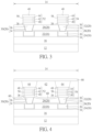
- FIGS. 1 - 4 illustrate a method for fabricating a semiconductor device according to an embodiment of the present invention.
- FIGS. 5 - 10 illustrate structural views of a semiconductor device according to different embodiments of the present invention.
- FIGS. 1 - 4 illustrate a method for fabricating a semiconductor device, or more specifically a MRAM device according to an embodiment of the present invention.
- a substrate 12 made of semiconductor material is first provided, in which the semiconductor material could be selected from the group consisting of silicon (Si), germanium (Ge), Si—Ge compounds, silicon carbide (SiC), and gallium arsenide (GaAs), and a MTJ region 14 and a logic region (not shown) are defined on the substrate 12 .
- MOS transistors metal-oxide semiconductor (MOS) transistors, passive devices, conductive layers, and interlayer dielectric (ILD) layer 16 could also be formed on top of the substrate 12 .
- MOS transistors metal-oxide semiconductor (MOS) transistors, passive devices, conductive layers, and interlayer dielectric (ILD) layer 16 could also be formed on top of the substrate 12 .
- MOS transistors planar MOS transistors or non-planar (such as FinFETs) MOS transistors could be formed on the substrate 12 , in which the MOS transistors could include transistor elements such as gate structures (for example metal gates) and source/drain region, spacer, epitaxial layer, and contact etch stop layer (CESL).
- the ILD layer 16 could be formed on the substrate 12 to cover the MOS transistors, and a plurality of contact plugs could be formed in the ILD layer 16 to electrically connect to the gate structure and/or source/drain region of MOS transistors. Since the fabrication of planar or non-planar transistors and
- metal interconnect structures 18 , 20 are sequentially formed on the ILD layer 16 to electrically connect the aforementioned contact plugs, in which the metal interconnect structure 18 includes an inter-metal dielectric (IMD) layer 22 and metal interconnections 24 embedded in the IMD layer 22 , and the metal interconnect structure 20 includes a stop layer 26 , an IMD layer 28 , and metal interconnections 30 , 32 embedded in the stop layer 26 and the IMD layer 28 .
- IMD inter-metal dielectric
- each of the metal interconnections 24 from the metal interconnect structure 18 preferably includes a trench conductor and each of the metal interconnections 30 , 32 from the metal interconnect structure 20 includes a via conductor.
- each of the metal interconnections 24 , 30 , 32 from the metal interconnect structures 18 , 20 could be embedded within the IMD layers 22 , 28 and/or stop layer 26 according to a single damascene process or dual damascene process.
- each of the metal interconnections 24 , 30 , 32 could further include a barrier layer 34 and a metal layer 36 , in which the barrier layer 34 could be selected from the group consisting of titanium (Ti), titanium nitride (TiN), tantalum (Ta), and tantalum nitride (TaN) and the metal layer 36 could be selected from the group consisting of tungsten (W), copper (Cu), aluminum (Al), titanium aluminide (TiAl), and cobalt tungsten phosphide (CoWP). Since single damascene process and dual damascene process are well known to those skilled in the art, the details of which are not explained herein for the sake of brevity.
- the metal layers 36 in the metal interconnections 24 are preferably made of copper
- the metal layers 36 in the metal interconnections 30 , 32 are preferably made of tungsten
- the IMD layers 22 , 28 are preferably made of silicon oxide or ultra low-k (ULK) dielectric layer
- the stop layers 26 is preferably made of nitrogen doped carbide (NDC), silicon nitride, silicon carbon nitride (SiCN), or combination thereof.
- a bottom electrode 38 is formed on the surface of the IMD layer 28 , a MTJ stack 46 including a pinned layer 40 , a barrier layer 42 , and a free layer 44 is formed on the bottom electrode 38 , a top electrode 48 is formed on the MTJ stack 46 , and a patterned mask 50 such as a patterned resist is formed on the surface of the top electrode 48 .
- the free layer 44 could further include a first free layer (not shown) disposed on the barrier layer 42 , a stop layer (not shown) disposed on the first free layer, and a second free layer (not shown) disposed on the stop layer.
- the bottom electrode 38 and the top electrode 48 are preferably made of conductive material including but not limited to for example Ta, Pt, Cu, Au, Al, or combination thereof.
- the pinned layer 40 could be made of ferromagnetic material including but not limited to for example iron, cobalt, nickel, or alloys thereof such as cobalt-iron-boron (CoFeB) or cobalt-iron (CoFe), in which the pinned layer 40 is formed to fix or limit the direction of magnetic moment of adjacent layers.
- the barrier layer 42 could be made of insulating material including but not limited to for example oxides such as aluminum oxide (AlO x ) or magnesium oxide (MgO).
- the free layer 44 including the first free layer and the second free layer could be made of ferromagnetic material including but not limited to for example iron, cobalt, nickel, or alloys thereof such as cobalt-iron-boron (CoFeB) or nickel-iron (NiFe), in which the magnetized direction of the free layer 44 could be altered freely depending on the influence of outside magnetic field.
- ferromagnetic material including but not limited to for example iron, cobalt, nickel, or alloys thereof such as cobalt-iron-boron (CoFeB) or nickel-iron (NiFe), in which the magnetized direction of the free layer 44 could be altered freely depending on the influence of outside magnetic field.
- an etching process is conducted by using the patterned mask 50 as mask to remove part of the top electrode 48 , part of the MTJ stack 46 , and part of the bottom electrode 38 to form a plurality of MTJs 52 , 54 , a deposition process is conducted to form polymers 56 on sidewalls of each of the MTJs 52 , 54 , and then repeating the aforementioned etching process and deposition process interchangeably.
- the etching process preferably uses hydrochloric acid (HCl) and/or chlorine gas (Cl 2 ) to remove or pattern part of the top electrode 48 , part of the MTJ stack 46 , and part of the bottom electrode 38 to form MTJs 52 , 54 and the deposition process preferably injects chloromethane (CH 3 Cl) to form polymers 56 on sidewalls of the MTJs 52 , 54 , in which the polymers 56 preferably include polymers containing carbon bonds and/or hydrogen bonds.
- HCl hydrochloric acid
- Cl 2 chlorine gas
- etching process is conducted by using sulfuric acid (H 2 SO 4 ) and/or hydrofluoric acid (HF) to completely remove the polymers 56 formed or accumulated during the aforementioned etching process and deposition process.
- H 2 SO 4 sulfuric acid
- HF hydrofluoric acid
- the etching process and deposition process conducted previously further forms rough surfaces 58 on sidewalls of the MTJs 52 , 54 and as the polymers 56 are removed the rough surfaces 58 are also exposed.
- the rough surfaces 58 could include different profile or textures depending on the recipe or parameters used during the etching process.
- the rough surfaces 58 could include jagged or wavy surfaces in this embodiment, but not limited thereto.
- the present invention preferably omits the conventional ME and/or IBE process by repeating the aforementioned etching process of using HCl and/or Cl 2 and deposition process of injecting CH 3 Cl to pattern the MTJ stack 46 for forming the MTJs 52 , 54 and at the same time forms polymers 56 on sidewalls of the MTJs 52 , 54 so that the sidewalls of the MTJs 52 , 54 could be protected from re-sputter of metal ions from causing damages.
- ME reactive ion etching
- IBE ion beam etching
- a cap layer 60 is formed on the MTJs 52 , 54 to cover the surface of the IMD layer 28 , an IMD layer 62 is formed on the cap layer 60 , and one or more photo-etching process is conducted to remove part of the IMD layer 62 and part of the cap layer 60 to form contact holes (not shown) exposing the top electrodes 48 .
- conductive materials are deposited into the contact holes and planarizing process such as chemical mechanical polishing (CMP) process is conducted to form metal interconnections 64 contacting the top electrodes 48 underneath.
- CMP chemical mechanical polishing
- another stop layer 66 is formed on the IMD layer 62 and covering the metal interconnections 64 .
- the cap layer 60 preferably includes silicon nitride, but could also include other dielectric material including but not limited to for example silicon oxide, silicon oxynitride (SiON), or SiCN depending on the demand of the product.
- the stop layer 66 could include nitrogen doped carbide (NDC), silicon nitride, silicon carbon nitride (SiCN), and most preferably SiCN. Similar to the aforementioned metal interconnections, the metal interconnections 64 could be formed in the IMD layer 62 according to a single damascene process or dual damascene process.
- each of the metal interconnection 64 could further include a barrier layer and a metal layer, in which the barrier layer could be selected from the group consisting of titanium (Ti), titanium nitride (TiN), tantalum (Ta), and tantalum nitride (TaN) and the metal layer could be selected from the group consisting of tungsten (W), copper (Cu), aluminum (Al), titanium aluminide (TiAl), and cobalt tungsten phosphide (CoWP).
- the barrier layer could be selected from the group consisting of titanium (Ti), titanium nitride (TiN), tantalum (Ta), and tantalum nitride (TaN)
- the metal layer could be selected from the group consisting of tungsten (W), copper (Cu), aluminum (Al), titanium aluminide (TiAl), and cobalt tungsten phosphide (CoWP).
- FIGS. 5 - 7 illustrate structural views of a semiconductor device according to different embodiments of the present invention.
- each of the MTJs such as the MTJ 52 is disposed on the substrate 12
- a bottom electrode 38 is disposed under the MTJ 52
- a top electrode 48 is disposed on the MTJ 52
- the MTJ 52 includes a pinned layer 40 on the metal interconnection 30 , a barrier layer 42 on the pinned layer 40 , a free layer 44 on the barrier layer 42 , and rough surfaces 58 on sidewalls of the MTJ 52 .
- the rough surfaces 58 could only appear on sidewalls of the pinned layer 40 in FIG. 5
- the rough surfaces 58 could only appear on sidewalls of the barrier layer 42 in FIG. 6
- the rough surfaces 58 could only appear on sidewalls of the free layer 44 in FIG. 7 , which are all within the scope of the present invention.
- FIGS. 8 - 10 illustrate structural views of a semiconductor device according to different embodiments of the present invention.
- FIGS. 8 - 10 in contrast to rough surfaces 58 only appear on one of the pinned layer 40 , barrier layer 42 , or free layer 44 as disclosed in the aforementioned embodiment, according to other embodiments of the present invention it would also be desirable to adjust the parameter of the etching process corresponding to each of the material layers so that the rough surfaces 58 could appear on part of the pinned layer 40 , barrier layer 42 , and/or free layer 44 at the same time.
- the rough surfaces 58 could appear on both pinned layer 40 and free layer 44 at the same time while the sidewalls of the of the barrier layer 42 still remained to be planar in FIG. 8
- the rough surfaces 58 could appear on both pinned layer 40 and barrier layer 42 at the same time while the sidewalls of the free layer 44 still remained to be planar in FIG. 9
- the rough surfaces 58 could appear on both barrier layer 42 and free layer 40 at the same time while the sidewalls of the pinned layer 40 still remained to be planar in FIG. 10 , which are all within the scope of the present invention.
- the rough surfaces 58 in contrast to that the rough surfaces 58 only appear on sidewalls of the MTJs 52 , 54 , it would also be desirable to adjust the parameter or selectivity of the etching process so that the rough surfaces could appear not only on sidewalls of the MTJs 52 , 54 but also on sidewalls of the bottom electrodes 38 and/or top electrodes 48 , which are all within the scope of the present invention.
- the present invention preferably omits the conventional RIE and/or IBE process by repeating the aforementioned etching process of using HCl and/or Cl 2 and deposition process of injecting CH 3 Cl to pattern the MTJ stack 46 for forming the MTJs 52 , 54 and at the same time forms polymers 56 on sidewalls of the MTJs 52 , 54 so that the sidewalls of the MTJs 52 , 54 could be protected from re-sputter of metal ions from during the patterning process.
- RIE reactive ion etching
- IBE ion beam etching
Landscapes
- Engineering & Computer Science (AREA)
- Manufacturing & Machinery (AREA)
- Hall/Mr Elements (AREA)
- Mram Or Spin Memory Techniques (AREA)
Abstract
Description
Claims (7)
Priority Applications (2)
| Application Number | Priority Date | Filing Date | Title |
|---|---|---|---|
| US18/239,119 US12178136B2 (en) | 2020-07-07 | 2023-08-28 | Semiconductor device and method for fabricating the same |
| US18/946,936 US20250072294A1 (en) | 2020-07-07 | 2024-11-14 | Semiconductor device and method for fabricating the same |
Applications Claiming Priority (2)
| Application Number | Priority Date | Filing Date | Title |
|---|---|---|---|
| CN202010645397.5A CN113903763B (en) | 2020-07-07 | 2020-07-07 | Semiconductor element and manufacturing method thereof |
| CN202010645397.5 | 2020-07-07 |
Related Child Applications (1)
| Application Number | Title | Priority Date | Filing Date |
|---|---|---|---|
| US18/239,119 Division US12178136B2 (en) | 2020-07-07 | 2023-08-28 | Semiconductor device and method for fabricating the same |
Publications (2)
| Publication Number | Publication Date |
|---|---|
| US20220013715A1 US20220013715A1 (en) | 2022-01-13 |
| US11778917B2 true US11778917B2 (en) | 2023-10-03 |
Family
ID=79173032
Family Applications (3)
| Application Number | Title | Priority Date | Filing Date |
|---|---|---|---|
| US16/985,206 Active 2041-01-05 US11778917B2 (en) | 2020-07-07 | 2020-08-04 | Semiconductor device and method for fabricating the same |
| US18/239,119 Active US12178136B2 (en) | 2020-07-07 | 2023-08-28 | Semiconductor device and method for fabricating the same |
| US18/946,936 Pending US20250072294A1 (en) | 2020-07-07 | 2024-11-14 | Semiconductor device and method for fabricating the same |
Family Applications After (2)
| Application Number | Title | Priority Date | Filing Date |
|---|---|---|---|
| US18/239,119 Active US12178136B2 (en) | 2020-07-07 | 2023-08-28 | Semiconductor device and method for fabricating the same |
| US18/946,936 Pending US20250072294A1 (en) | 2020-07-07 | 2024-11-14 | Semiconductor device and method for fabricating the same |
Country Status (2)
| Country | Link |
|---|---|
| US (3) | US11778917B2 (en) |
| CN (1) | CN113903763B (en) |
Citations (8)
| Publication number | Priority date | Publication date | Assignee | Title |
|---|---|---|---|---|
| US8492169B2 (en) * | 2011-08-15 | 2013-07-23 | Magic Technologies, Inc. | Magnetic tunnel junction for MRAM applications |
| US8536063B2 (en) | 2011-08-30 | 2013-09-17 | Avalanche Technology Inc. | MRAM etching processes |
| US20150104882A1 (en) * | 2013-10-10 | 2015-04-16 | Avalanche Technology Inc. | Fabrication method for high-density mram using thin hard mask |
| US9153453B2 (en) | 2011-02-11 | 2015-10-06 | Brookhaven Science Associates, Llc | Technique for etching monolayer and multilayer materials |
| US20170263861A1 (en) * | 2016-03-10 | 2017-09-14 | Jeong-Heon Park | Method of fabricating memory device |
| US20190165258A1 (en) * | 2017-11-30 | 2019-05-30 | Taiwan Semiconductor Manufacturing Co., Ltd. | Memory device and fabrication method thereof |
| US20200235291A1 (en) * | 2016-11-02 | 2020-07-23 | Samsung Electronics Co., Ltd. | Data storage devices and methods for manufacturing the same |
| US20210175412A1 (en) * | 2019-12-10 | 2021-06-10 | HeFeChip Corporation Limited | Magnetic memory device with multiple sidewall spacers covering sidewall of mtj element and method for manufacturing the same |
Family Cites Families (6)
| Publication number | Priority date | Publication date | Assignee | Title |
|---|---|---|---|---|
| KR100943860B1 (en) * | 2007-12-21 | 2010-02-24 | 주식회사 하이닉스반도체 | Magnetic tunnel junction cell formation method |
| EP2457932A1 (en) * | 2009-07-21 | 2012-05-30 | Sumitomo Bakelite Company Limited | Composition for film formation, insulating film, and semiconductor device |
| JP2012204408A (en) * | 2011-03-23 | 2012-10-22 | Toshiba Corp | Manufacturing method of semiconductor device |
| KR101870873B1 (en) * | 2011-08-04 | 2018-07-20 | 에스케이하이닉스 주식회사 | Method for fabricating magnetic tunnel junction device |
| US9647200B1 (en) * | 2015-12-07 | 2017-05-09 | International Business Machines Corporation | Encapsulation of magnetic tunnel junction structures in organic photopatternable dielectric material |
| US10522751B2 (en) * | 2018-05-22 | 2019-12-31 | Taiwan Semiconductor Manufacturing Company, Ltd. | MTJ CD variation by HM trimming |
-
2020
- 2020-07-07 CN CN202010645397.5A patent/CN113903763B/en active Active
- 2020-08-04 US US16/985,206 patent/US11778917B2/en active Active
-
2023
- 2023-08-28 US US18/239,119 patent/US12178136B2/en active Active
-
2024
- 2024-11-14 US US18/946,936 patent/US20250072294A1/en active Pending
Patent Citations (8)
| Publication number | Priority date | Publication date | Assignee | Title |
|---|---|---|---|---|
| US9153453B2 (en) | 2011-02-11 | 2015-10-06 | Brookhaven Science Associates, Llc | Technique for etching monolayer and multilayer materials |
| US8492169B2 (en) * | 2011-08-15 | 2013-07-23 | Magic Technologies, Inc. | Magnetic tunnel junction for MRAM applications |
| US8536063B2 (en) | 2011-08-30 | 2013-09-17 | Avalanche Technology Inc. | MRAM etching processes |
| US20150104882A1 (en) * | 2013-10-10 | 2015-04-16 | Avalanche Technology Inc. | Fabrication method for high-density mram using thin hard mask |
| US20170263861A1 (en) * | 2016-03-10 | 2017-09-14 | Jeong-Heon Park | Method of fabricating memory device |
| US20200235291A1 (en) * | 2016-11-02 | 2020-07-23 | Samsung Electronics Co., Ltd. | Data storage devices and methods for manufacturing the same |
| US20190165258A1 (en) * | 2017-11-30 | 2019-05-30 | Taiwan Semiconductor Manufacturing Co., Ltd. | Memory device and fabrication method thereof |
| US20210175412A1 (en) * | 2019-12-10 | 2021-06-10 | HeFeChip Corporation Limited | Magnetic memory device with multiple sidewall spacers covering sidewall of mtj element and method for manufacturing the same |
Also Published As
| Publication number | Publication date |
|---|---|
| CN113903763A (en) | 2022-01-07 |
| US20230403942A1 (en) | 2023-12-14 |
| US20250072294A1 (en) | 2025-02-27 |
| US12178136B2 (en) | 2024-12-24 |
| US20220013715A1 (en) | 2022-01-13 |
| CN113903763B (en) | 2025-08-19 |
Similar Documents
| Publication | Publication Date | Title |
|---|---|---|
| US11508904B2 (en) | Semiconductor device and method for fabricating the same | |
| US11476411B2 (en) | Semiconductor device and method for fabricating the same | |
| US11616193B2 (en) | Semiconductor device and method for fabricating the same | |
| US10529920B1 (en) | Semiconductor device and method for fabricating the same | |
| US11778922B2 (en) | Semiconductor device and method for fabricating the same | |
| US11968911B2 (en) | Semiconductor device and method for fabricating the same | |
| US12349367B2 (en) | Semiconductor device and method for fabricating the same | |
| US20250194434A1 (en) | Magnetoresistive random access memory and method for fabricating the same | |
| US11968906B2 (en) | Semiconductor device and method for fabricating the same | |
| US11821964B2 (en) | Magnetoresistive random access memory and method for fabricating the same | |
| US12178136B2 (en) | Semiconductor device and method for fabricating the same | |
| US11871677B2 (en) | Method for fabricating semiconductor device |
Legal Events
| Date | Code | Title | Description |
|---|---|---|---|
| AS | Assignment |
Owner name: UNITED MICROELECTRONICS CORP., TAIWAN Free format text: ASSIGNMENT OF ASSIGNORS INTEREST;ASSIGNORS:LIU, CHIA-WEI;FANG, JIA-FENG;LIN, CHUN-HSIEN;REEL/FRAME:053401/0425 Effective date: 20200731 |
|
| FEPP | Fee payment procedure |
Free format text: ENTITY STATUS SET TO UNDISCOUNTED (ORIGINAL EVENT CODE: BIG.); ENTITY STATUS OF PATENT OWNER: LARGE ENTITY |
|
| STPP | Information on status: patent application and granting procedure in general |
Free format text: NON FINAL ACTION MAILED |
|
| STPP | Information on status: patent application and granting procedure in general |
Free format text: RESPONSE TO NON-FINAL OFFICE ACTION ENTERED AND FORWARDED TO EXAMINER |
|
| STPP | Information on status: patent application and granting procedure in general |
Free format text: FINAL REJECTION MAILED |
|
| STPP | Information on status: patent application and granting procedure in general |
Free format text: DOCKETED NEW CASE - READY FOR EXAMINATION |
|
| STPP | Information on status: patent application and granting procedure in general |
Free format text: NOTICE OF ALLOWANCE MAILED -- APPLICATION RECEIVED IN OFFICE OF PUBLICATIONS |
|
| STPP | Information on status: patent application and granting procedure in general |
Free format text: PUBLICATIONS -- ISSUE FEE PAYMENT VERIFIED |
|
| STCF | Information on status: patent grant |
Free format text: PATENTED CASE |