US11757367B2 - Flyback switch circuit and control method thereof - Google Patents
Flyback switch circuit and control method thereof Download PDFInfo
- Publication number
- US11757367B2 US11757367B2 US17/476,482 US202117476482A US11757367B2 US 11757367 B2 US11757367 B2 US 11757367B2 US 202117476482 A US202117476482 A US 202117476482A US 11757367 B2 US11757367 B2 US 11757367B2
- Authority
- US
- United States
- Prior art keywords
- transistor
- voltage
- circuit
- main power
- signal
- Prior art date
- Legal status (The legal status is an assumption and is not a legal conclusion. Google has not performed a legal analysis and makes no representation as to the accuracy of the status listed.)
- Active, expires
Links
- 238000000034 method Methods 0.000 title claims abstract description 30
- 238000004804 winding Methods 0.000 claims description 82
- 238000001514 detection method Methods 0.000 claims description 39
- 239000003990 capacitor Substances 0.000 claims description 28
- 238000005070 sampling Methods 0.000 claims description 11
- 230000010355 oscillation Effects 0.000 description 29
- 238000010586 diagram Methods 0.000 description 24
- 230000008878 coupling Effects 0.000 description 23
- 238000010168 coupling process Methods 0.000 description 23
- 238000005859 coupling reaction Methods 0.000 description 23
- 230000003071 parasitic effect Effects 0.000 description 13
- 239000008186 active pharmaceutical agent Substances 0.000 description 9
- 230000001360 synchronised effect Effects 0.000 description 5
- JMASRVWKEDWRBT-UHFFFAOYSA-N Gallium nitride Chemical group [Ga]#N JMASRVWKEDWRBT-UHFFFAOYSA-N 0.000 description 3
- 230000003044 adaptive effect Effects 0.000 description 3
- 238000005516 engineering process Methods 0.000 description 3
- 229910002601 GaN Inorganic materials 0.000 description 2
- 230000003247 decreasing effect Effects 0.000 description 2
- 230000003111 delayed effect Effects 0.000 description 2
- 230000000694 effects Effects 0.000 description 2
- 230000004048 modification Effects 0.000 description 2
- 238000012986 modification Methods 0.000 description 2
- 230000008569 process Effects 0.000 description 2
- 230000002441 reversible effect Effects 0.000 description 2
- XUIMIQQOPSSXEZ-UHFFFAOYSA-N Silicon Chemical compound [Si] XUIMIQQOPSSXEZ-UHFFFAOYSA-N 0.000 description 1
- 230000005540 biological transmission Effects 0.000 description 1
- 230000008859 change Effects 0.000 description 1
- 230000010354 integration Effects 0.000 description 1
- 230000008844 regulatory mechanism Effects 0.000 description 1
- 229910052710 silicon Inorganic materials 0.000 description 1
- 239000010703 silicon Substances 0.000 description 1
- 238000006467 substitution reaction Methods 0.000 description 1
- 230000036962 time dependent Effects 0.000 description 1
Images


Classifications
-
- H—ELECTRICITY
- H02—GENERATION; CONVERSION OR DISTRIBUTION OF ELECTRIC POWER
- H02M—APPARATUS FOR CONVERSION BETWEEN AC AND AC, BETWEEN AC AND DC, OR BETWEEN DC AND DC, AND FOR USE WITH MAINS OR SIMILAR POWER SUPPLY SYSTEMS; CONVERSION OF DC OR AC INPUT POWER INTO SURGE OUTPUT POWER; CONTROL OR REGULATION THEREOF
- H02M3/00—Conversion of DC power input into DC power output
- H02M3/22—Conversion of DC power input into DC power output with intermediate conversion into AC
- H02M3/24—Conversion of DC power input into DC power output with intermediate conversion into AC by static converters
- H02M3/28—Conversion of DC power input into DC power output with intermediate conversion into AC by static converters using discharge tubes with control electrode or semiconductor devices with control electrode to produce the intermediate AC
- H02M3/325—Conversion of DC power input into DC power output with intermediate conversion into AC by static converters using discharge tubes with control electrode or semiconductor devices with control electrode to produce the intermediate AC using devices of a triode or a transistor type requiring continuous application of a control signal
- H02M3/335—Conversion of DC power input into DC power output with intermediate conversion into AC by static converters using discharge tubes with control electrode or semiconductor devices with control electrode to produce the intermediate AC using devices of a triode or a transistor type requiring continuous application of a control signal using semiconductor devices only
- H02M3/33569—Conversion of DC power input into DC power output with intermediate conversion into AC by static converters using discharge tubes with control electrode or semiconductor devices with control electrode to produce the intermediate AC using devices of a triode or a transistor type requiring continuous application of a control signal using semiconductor devices only having several active switching elements
- H02M3/33576—Conversion of DC power input into DC power output with intermediate conversion into AC by static converters using discharge tubes with control electrode or semiconductor devices with control electrode to produce the intermediate AC using devices of a triode or a transistor type requiring continuous application of a control signal using semiconductor devices only having several active switching elements having at least one active switching element at the secondary side of an isolation transformer
- H02M3/33592—Conversion of DC power input into DC power output with intermediate conversion into AC by static converters using discharge tubes with control electrode or semiconductor devices with control electrode to produce the intermediate AC using devices of a triode or a transistor type requiring continuous application of a control signal using semiconductor devices only having several active switching elements having at least one active switching element at the secondary side of an isolation transformer having a synchronous rectifier circuit or a synchronous freewheeling circuit at the secondary side of an isolation transformer
-
- H—ELECTRICITY
- H02—GENERATION; CONVERSION OR DISTRIBUTION OF ELECTRIC POWER
- H02M—APPARATUS FOR CONVERSION BETWEEN AC AND AC, BETWEEN AC AND DC, OR BETWEEN DC AND DC, AND FOR USE WITH MAINS OR SIMILAR POWER SUPPLY SYSTEMS; CONVERSION OF DC OR AC INPUT POWER INTO SURGE OUTPUT POWER; CONTROL OR REGULATION THEREOF
- H02M3/00—Conversion of DC power input into DC power output
- H02M3/22—Conversion of DC power input into DC power output with intermediate conversion into AC
- H02M3/24—Conversion of DC power input into DC power output with intermediate conversion into AC by static converters
- H02M3/28—Conversion of DC power input into DC power output with intermediate conversion into AC by static converters using discharge tubes with control electrode or semiconductor devices with control electrode to produce the intermediate AC
- H02M3/325—Conversion of DC power input into DC power output with intermediate conversion into AC by static converters using discharge tubes with control electrode or semiconductor devices with control electrode to produce the intermediate AC using devices of a triode or a transistor type requiring continuous application of a control signal
- H02M3/335—Conversion of DC power input into DC power output with intermediate conversion into AC by static converters using discharge tubes with control electrode or semiconductor devices with control electrode to produce the intermediate AC using devices of a triode or a transistor type requiring continuous application of a control signal using semiconductor devices only
- H02M3/33569—Conversion of DC power input into DC power output with intermediate conversion into AC by static converters using discharge tubes with control electrode or semiconductor devices with control electrode to produce the intermediate AC using devices of a triode or a transistor type requiring continuous application of a control signal using semiconductor devices only having several active switching elements
-
- H—ELECTRICITY
- H02—GENERATION; CONVERSION OR DISTRIBUTION OF ELECTRIC POWER
- H02M—APPARATUS FOR CONVERSION BETWEEN AC AND AC, BETWEEN AC AND DC, OR BETWEEN DC AND DC, AND FOR USE WITH MAINS OR SIMILAR POWER SUPPLY SYSTEMS; CONVERSION OF DC OR AC INPUT POWER INTO SURGE OUTPUT POWER; CONTROL OR REGULATION THEREOF
- H02M1/00—Details of apparatus for conversion
- H02M1/0048—Circuits or arrangements for reducing losses
- H02M1/0054—Transistor switching losses
- H02M1/0058—Transistor switching losses by employing soft switching techniques, i.e. commutation of transistors when applied voltage is zero or when current flow is zero
-
- H—ELECTRICITY
- H02—GENERATION; CONVERSION OR DISTRIBUTION OF ELECTRIC POWER
- H02M—APPARATUS FOR CONVERSION BETWEEN AC AND AC, BETWEEN AC AND DC, OR BETWEEN DC AND DC, AND FOR USE WITH MAINS OR SIMILAR POWER SUPPLY SYSTEMS; CONVERSION OF DC OR AC INPUT POWER INTO SURGE OUTPUT POWER; CONTROL OR REGULATION THEREOF
- H02M1/00—Details of apparatus for conversion
- H02M1/08—Circuits specially adapted for the generation of control voltages for semiconductor devices incorporated in static converters
- H02M1/083—Circuits specially adapted for the generation of control voltages for semiconductor devices incorporated in static converters for the ignition at the zero crossing of the voltage or the current
-
- H—ELECTRICITY
- H02—GENERATION; CONVERSION OR DISTRIBUTION OF ELECTRIC POWER
- H02M—APPARATUS FOR CONVERSION BETWEEN AC AND AC, BETWEEN AC AND DC, OR BETWEEN DC AND DC, AND FOR USE WITH MAINS OR SIMILAR POWER SUPPLY SYSTEMS; CONVERSION OF DC OR AC INPUT POWER INTO SURGE OUTPUT POWER; CONTROL OR REGULATION THEREOF
- H02M1/00—Details of apparatus for conversion
- H02M1/32—Means for protecting converters other than automatic disconnection
- H02M1/34—Snubber circuits
- H02M1/342—Active non-dissipative snubbers
-
- Y—GENERAL TAGGING OF NEW TECHNOLOGICAL DEVELOPMENTS; GENERAL TAGGING OF CROSS-SECTIONAL TECHNOLOGIES SPANNING OVER SEVERAL SECTIONS OF THE IPC; TECHNICAL SUBJECTS COVERED BY FORMER USPC CROSS-REFERENCE ART COLLECTIONS [XRACs] AND DIGESTS
- Y02—TECHNOLOGIES OR APPLICATIONS FOR MITIGATION OR ADAPTATION AGAINST CLIMATE CHANGE
- Y02B—CLIMATE CHANGE MITIGATION TECHNOLOGIES RELATED TO BUILDINGS, e.g. HOUSING, HOUSE APPLIANCES OR RELATED END-USER APPLICATIONS
- Y02B70/00—Technologies for an efficient end-user side electric power management and consumption
- Y02B70/10—Technologies improving the efficiency by using switched-mode power supplies [SMPS], i.e. efficient power electronics conversion e.g. power factor correction or reduction of losses in power supplies or efficient standby modes
Definitions
- the present disclosure relates to the technical field of power electronics technology, and more particularly, to a flyback switching circuit and a control method thereof.
- a flyback switching circuit includes a main power transistor, which provides energy to a load through turn-on and turn-off of the main transistor. Controlling switch state of the main power transistor is a control core of the flyback switching circuit. How to effectively control the switch state of the main power transistor to reduce turn-off loss of the main transistor is a very challenging job.
- an active clamping flyback circuit in a prior art is shown, which is the flyback switching circuit coupling to a clamping circuit and a clamping control circuit, the clamping circuit comprises a first capacitor and a first transistor coupling in series, one end of the first capacitor is coupling to a high voltage end of an input voltage, one end of the first transistor is coupling to a common end of a main transistor and a primary winding of a transformer.
- the main transistor turns off, instantaneous spikes and high secondary harmonics at a drain terminal of the main transistor are capacitively coupling to a power supply, thus clamping a drain voltage Vdssw of the main transistor, so that the turn-off loss of the main transistor is reduced and a system efficiency is improved.
- a turn-off time of the first transistor cannot be accurately controlled before the main power transistor is turned on.
- a voltage of a common end of the main power transistor and the primary winding may be relatively large. If the main power transistor is turned on at this time, a large energy loss generates an entire power supply system, thereby affecting the system efficiency.
- the first transistor when system is operating in a discontinuous conduction mode (DCM), the first transistor is off in advance, and the drain voltage Vdssw of the main transistor may be dropped and restored, so that causing energy loss and the system efficiency is reduced.
- delaying turn-off may cause severity of the oscillation, or insufficient transmission of energy of this cycle, so that decreasing the system efficiency, even causing operation failure. Therefore, how to control the first transistor to be off when current of the primary winding of the transformer reaches zero is an urgent problem to be solved in the flyback active clamping circuit operating in the discontinuous conduction mode.
- an objective of the disclosure is to provide a flyback switching circuit and a control method thereof to adjust the off-time of the first transistor and thusly reduce a turn-on loss of the main transistor, thereby solving technical problems of large turn-on loss of the main transistor and low system efficiency in the flyback switching circuit in the prior art.
- an active clamping flyback circuit comprising a flyback circuit, a clamping circuit and a clamping control circuit, wherein the flyback circuit comprises a transformer, a main transistor, and a freewheeling diode or a synchronous rectifier.
- An output feedback circuit is coupling to an auxiliary winding of the transformer and outputs a feedback voltage through a divided voltage.
- the clamping circuit comprises a first capacitor and a first transistor coupling in series, wherein one end of the first capacitor is coupling to a high voltage end of an input voltage, and one end of the first transistor is coupling to a common end of the main transistor and a primary winding of the transformer.
- the clamping control circuit starts timing when the first transistor is off, and ends timing until the feedback voltage is reduced from positive voltage to zero voltage, wherein time elapsed for the timing is a first time, and the clamping control circuit adjusts a turn-off time of next switching cycle of the first transistor so that the first time of the next switching cycle is configured to be substantially the same as a first threshold.
- the first threshold is a quarter of an oscillation period, and a sum of a magnetizing inductance and a leakage inductance of the transformer (Lm+Lk) and a sum of a drain-source parasitic capacitance of the first transistor and a drain-source parasitic capacitance of the main transistor (Cdssa+Cdssw) generate an oscillation, so that generating the oscillation period.
- the clamping control circuit comprises a first resistor to set the first threshold, a voltage of the first resistor indicates the oscillation period.
- the clamping control circuit comprises a comparison circuit to compare the feedback voltage to a first voltage threshold, the first voltage threshold is a zero or a near-zero voltage.
- the clamping control circuit comprises a timing circuit to start timing when the first transistor is off, and end timing until the feedback voltage is reduced from positive voltage to zero voltage, time elapsed for the timing is the first time.
- the main transistor is turned on when the feedback voltage oscillates to a valley or near the valley.
- a control method for an active clamping flyback circuit wherein the active clamping flyback circuit comprises a flyback circuit, a clamping circuit and a clamping control circuit.
- the flyback circuit comprises a transformer, a main transistor, and a freewheeling diode or a synchronous rectifier.
- An output feedback circuit is coupling to an auxiliary winding of the transformer and outputs a feedback voltage through a divided voltage.
- the clamping circuit comprises a first capacitor and a first transistor coupling in series, wherein one end of the first capacitor is coupling to a high voltage end of an input voltage, and one end of the first transistor is coupling to a common end of the main transistor and a primary winding of the transformer.
- the method includes: starting timing when the first transistor is off, and ending timing until the feedback voltage is reduced from a positive voltage to zero voltage, wherein time elapsed for the timing is a first time, and adjusting a turn-off time of next switching cycle of the first transistor so that the first time of the next switching cycle is configured to be substantially the same as a first threshold.
- the first threshold is a quarter of an oscillation period, and a sum of a magnetizing inductance and a leakage inductance of the transformer (Lm+Lk) and a sum of a drain-source parasitic capacitance of the first transistor and a drain-source parasitic capacitance of the main transistor (Cdssa+Cdssw) generate an oscillation, so that generating the oscillation period.
- the first threshold is set by a first resistor, a voltage of the first resistor indicates the oscillation period.
- the main transistor is on when the feedback voltage oscillates to a valley or near the valley.
- a flyback switching circuit comprises a main power transistor, a transformer and a secondary rectifying transistor, the transformer includes a primary winding and a secondary winding, the main power transistor is connected to the primary winding, and the secondary rectifying transistor is connected to the secondary winding, the flyback switching circuit further comprises:
- the first transistor is configured to adjust a drain-source voltage of the main power transistor
- the switch control unit is configured to control a switching state of the main power transistor and a switching state of the first transistor
- the switch control unit is further configured to adjust a turn-off time of the first transistor according to a reference value greater than zero to control a turn-on time voltage of the main power transistor.
- the switch control unit comprises a first bias voltage circuit and a turn-off adjustment circuit.
- the first bias voltage circuit is configured to output a first bias voltage signal greater than zero, and the first bias voltage signal serves as the reference value.
- the turn-off adjustment circuit is configured to receive the first bias voltage signal, and adjust the turn-off time of the first transistor according to the first bias voltage signal to control the turn-on time voltage of the main power transistor.
- the turn-off adjustment circuit adjusts the turn-off time of the first transistor, so that the drain-source voltage of the main power transistor is consistent with the first bias voltage signal before the main power transistor is turned on.
- the first bias voltage circuit outputs the first bias voltage signal of a predetermined value, and the predetermined value is greater than zero.
- the first bias voltage circuit outputs the adjustable first bias voltage signal, and a voltage value of the adjustable first bias voltage signal is greater than zero.
- the first bias voltage circuit receives an input voltage of the flyback switching circuit, and the adjustable first bias voltage signal is proportional to the input voltage.
- the switch control unit comprises a turn-off control circuit.
- the turn-off control circuit is configured to receive a first voltage signal characterizing a current of the primary winding, and compare the first voltage signal with a first reference voltage signal, and a comparison result serves a reset signal for controlling the first transistor to be turned off.
- the turn-off control circuit comprises a voltage detection circuit and an adjustment circuit.
- the voltage detection circuit is configured to receive the first bias voltage signal, detect a node voltage of the main power transistor, and output a voltage detection signal according to the node voltage of the main power transistor and the first bias voltage signal.
- the adjustment circuit is electrically connected to the turn-off control circuit and the voltage detection circuit, and is configured to adjust the turn-off time of the first transistor according to the voltage detection signal.
- the turn-off control circuit comprises a voltage detection circuit and a threshold adjustment circuit.
- the voltage detection circuit is configured to receive the first bias voltage signal, detect a node voltage of the main power transistor, and output a voltage detection signal according to the node voltage of the main power transistor and the first bias voltage signal.
- the threshold adjustment circuit is electrically connected to the voltage detection circuit and the turn-off control circuit, and the threshold adjustment circuit is configured to adjust a value of the first reference voltage signal according to the voltage detection signal, so that the turn-off time of the first transistor is adjusted.
- the switch control unit is further configured to compare the drain-source voltage of the main power transistor in a current cycle with the reference value, and adjust a pulse width of the first transistor in a next cycle adjacent to the current cycle according to a comparison result data.
- the switch control unit comprises:
- a calculation circuit configured to receive a second bias voltage signal, and providing the reference value according to the second bias voltage signal, an input signal, and an output signal;
- a comparison circuit configured to compare the reference value with the drain-source voltage of the main power transistor to obtain the comparison result data
- a pulse width adjustment circuit configured to adjust the pulse width of the first transistor in the next cycle according to the comparison result data, so as to control the turn-on time voltage of the main power transistor.
- V ZVS_ref (1 ⁇ k 1 )* V s_VIN ⁇ k 2 *V s_VO +V bias ,
- V ZVS_ref is the reference value
- V s_VIN is the input signal
- V s_VO is the output signal
- V bias is the second bias voltage signal
- k 1 is a first coefficient
- k 2 is a second coefficient.
- the calculation circuit is configured that the first coefficient and the second coefficient are adjustable, and the first coefficient and the second coefficient may be any values between 0% and 100%.
- a second auxiliary winding coupled to the transformer and a sampling circuit.
- the sampling circuit is configured to sample voltages of the second auxiliary winding to obtain a valley voltage characterizing the drain-source voltage, the input voltage and the output voltage.
- the voltage of the second auxiliary winding characterizes the input voltage when the main power transistor is turned on, and the voltage of the second auxiliary winding characterizes the output voltage when the main power transistor is turned off.
- the flyback switching circuit comprises a first capacitor and a clamping transistor, wherein the first capacitor and the clamping transistor are connected in series between a high potential end of an input power supply of the flyback switching circuit and a common node of the main power transistor and the primary winding, and the clamping transistor serves as the first transistor.
- the flyback switching circuit comprises a first auxiliary winding coupled to the transformer, an auxiliary transistor and a first auxiliary capacitor, the first auxiliary winding, wherein the auxiliary transistor and the first auxiliary capacitor are connected in series to form a loop, and the auxiliary transistor serves as the first transistor.
- a control method of a flyback switching circuit comprising a main power transistor, a transformer, a secondary rectifying transistor, and a first transistor configured for adjusting a drain-source voltage of the main power transistor.
- the control method comprising: adjusting a turn-off time of the first transistor according to a reference value greater than zero to control a turn-on time voltage of the main power transistor.
- control method of a flyback switching circuit further comprises: comparing a first voltage signal with a first reference voltage signal according to the first voltage signal characterizing a current of the primary winding, and a comparison result serves a reset signal for controlling the first transistor to be turned off; outputting a first bias voltage signal greater than zero, the first bias voltage signal serves as the reference value, adjusting the turn-off time of the first transistor according to the first bias voltage signal to control the turn-on time voltage of the main power transistor.
- control method of a flyback switching circuit further comprises:
- a step of obtaining the reference value comprises:
- V ZVS_ref (1 ⁇ k 1 )* V s_VIN ⁇ k 2 *V s_VO _+ V bias ,
- V ZVS_ref is the reference value
- V s_VIN is the input signal
- V s_VO is the output signal
- V bias is the second bias voltage signal
- k 1 is a first coefficient
- k 2 is a second coefficient.
- the first coefficient and the second coefficient are configured to be adjustable, and the first coefficient and the second coefficient are any values between 0% and 100%.
- the turn-off time of the first transistor may be adjusted by setting the reference value greater than zero, so that the drain-source voltage of the main power transistor is a preset value greater than zero before the main power transistor is turned on, thereby reducing the turn-on power consumption of the transistor and improving system efficiency.
- the circuit structure and the driving method of the disclosure has the following advantages: through starting timing from when the first transistor is off until the feedback voltage is reduced from a positive voltage to zero voltage, the time elapsed for timing is adjusted to be configured to be substantially the same as 1 ⁇ 4 oscillation period, so that the turn-off time of the first transistor is configured to be substantially the same as a time that current of the primary winding of the transformer is crossing zero, so that reducing system losses due to advanced turn-off or delayed turn-off of the first transistor and improving the system efficiency.
- FIG. 1 is a circuit diagram of an active clamping flyback circuit
- FIG. 2 is a circuit diagram of an active clamping flyback circuit according to an embodiment of the disclosure
- FIG. 3 shows waveforms of a DS voltage of a main transistor, a feedback voltage VFB, a driving voltage GSA of a first transistor, and a driving voltage GSW of the main transistor when the first transistor of the active clamping flyback circuit is off during a first time is greater than 1 ⁇ 4 of a oscillation period;
- FIG. 4 shows waveforms of a DS voltage of a main transistor, a feedback voltage VFB, a driving voltage GSA of a first transistor, and a driving voltage GSW of the main transistor when the first transistor of the active clamping flyback circuit is off during a first time is smaller than 1 ⁇ 4 of a oscillation period;
- FIG. 5 shows waveforms of a DS voltage of a main transistor, a feedback voltage VFB, a driving voltage GSA of a first transistor, and a driving voltage GSW of the main transistor when the first transistor of the active clamping flyback circuit is off during a first time is equal to 1 ⁇ 4 of a oscillation period;
- FIG. 6 is an implementation block diagram of an embodiment of a clamping control circuit
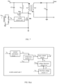
- FIG. 7 is a circuit block diagram of a flyback switch circuit according to a second embodiment of the present disclosure.
- FIG. 8 ( a ) is a circuit block diagram of a switch control unit according to a first embodiment of the present disclosure
- FIG. 8 ( b ) is a circuit diagram of an embodiment of the switch control unit in FIG. 8 ( a ) ;
- FIG. 9 ( a ) is a circuit block diagram of a switch control unit according to a second embodiment of the present disclosure.
- FIG. 9 ( b ) is a circuit diagram of an embodiment of the switch control unit in FIG. 9 ( a ) ;
- FIG. 10 is a working waveform diagram of the circuit block diagram in FIG. 8 ( a ) ;
- FIG. 11 ( a ) is a circuit block diagram of a flyback switch circuit according to a third embodiment of the present disclosure.
- FIG. 11 ( b ) is a block diagram of an embodiment of the switch control unit in FIG. 11 ( a ) ;
- FIG. 11 ( c ) is a control principle diagram of an embodiment of the flyback switch circuit in FIG. 11 ( a ) .
- a flyback switching circuit comprises a main power transistor, a transformer and a secondary rectifying transistor, wherein the transformer includes a primary winding and a secondary winding, the primary winding is connected to the primary winding, and the secondary rectifying transistor is connected to the secondary winding.
- the flyback switching circuit further comprises: a switch control unit and a first transistor in a primary side, the first transistor is configured to adjust a drain-source voltage of the main power transistor, and the switch control unit is configured to control a switching state of the main power transistor and a switching state of the first transistor, wherein, the switch control unit is further configured to adjust a turn-off time of the first transistor according to a reference value greater than zero to control a turn-on time voltage of the main power transistor.
- FIGS. 2 to 6 show an active clamping flyback circuit according to a first embodiment
- FIGS. 7 to 10 show a flyback switch circuit according to a second embodiment
- FIGS. 11 ( a ) to 11 ( c ) shows a flyback switch circuit according to a third embodiment.
- an active clamping flyback circuit which comprises a flyback circuit, a clamping circuit 100 and a clamping control circuit 200 , wherein the flyback circuit comprises a transformer T 1 , a main transistor M 1 , and a freewheeling diode or a synchronous rectifier transistor D 1 , an output feedback circuit is coupling to an auxiliary winding of the transformer and outputs a feedback voltage VFB through a divided voltage, the output feedback circuit is coupling to the clamping control circuit 200 ; the clamping circuit comprises a first capacitor CSA and a first transistor MSA that are coupling in series, one end of the first capacitor CSA is coupling to a high voltage end of an input voltage Vin, one end of the first transistor MSA is coupling to a common end of the main transistor M 1 and a primary winding of the transformer.
- the clamping control circuit starts timing when the first transistor MSA is off, and ends timing until the feedback voltage VFB is reduced from a positive voltage to a zero voltage, wherein time elapsed for the timing is a first time, and the clamping control circuit 200 adjusts turn-off time of the next switching cycle of the first transistor so that the first time of the next switching cycle configured to be substantially the same as a first threshold.
- Lm is an equivalent magnetizing inductance of the transformer
- Lk is a leakage inductance of the primary winding of the transformer
- Cp is a parasitic capacitance of the primary winding of the transformer T 1
- Cdssw is a drain-source parasitic capacitance of the main transistor M 1
- Cdssa is a drain-source parasitic capacitance of the first transistor MSA.
- Voltage of the auxiliary winding is divided by voltage dividing resistors RFB 1 and RFB 2 to obtain a feedback voltage VFB. In other embodiments, other voltage dividing methods may be configured to obtain the feedback voltage.
- the freewheeling diode D 1 is employed, and in other embodiments, the synchronous rectifier transistor may also be used for freewheeling.
- the first threshold is a quarter of an oscillation period, and a sum of a magnetizing inductance and a leakage inductance of the transformer (Lm+Lk) and a sum of a drain-source parasitic capacitance of the first transistor and a drain-source parasitic capacitance of the main transistor (Cdssa+Cdssw) generate an oscillation, so that generating the oscillation period.
- waveforms of a DS voltage of a main transistor, the feedback voltage VFB, a driving voltage GSA of the first transistor, and a driving voltage GSW of the main transistor when the first transistor of the active clamping flyback circuit is off during the first time is greater than 1 ⁇ 4 of a oscillation period are illustrated; when the first transistor is off during the first time is greater than 1 ⁇ 4 of the oscillation period, the DS voltage Vdssw of the main transistor may drop when the first transistor is off, resulting in energy loss, so that system efficiency is reduced.
- the feedback voltage VFB may cross zero when the above voltage drops, resulting the first time is misjudged. In order to prevent the first time from being misjudged, when the first transistor is off, a period of time is blanked to recover from the voltage drop, and then judge whether the feedback voltage VFB is from positive to negative.
- waveforms of a DS voltage of a main transistor, the feedback voltage VFB, the driving voltage GSA of the first transistor, and the driving voltage GSW of the main transistor when the first transistor of the active clamping flyback circuit is off during the first time is smaller than 1 ⁇ 4 of a oscillation period are illustrated; when the first transistor is off during the first time is smaller than 1 ⁇ 4 of the oscillation period, the DS voltage Vdssw of the main transistor may also drop when the first transistor is off, resulting in energy loss, so that the system efficiency is reduced.
- waveforms of a DS voltage of a main transistor, the feedback voltage VFB, the driving voltage GSA of the first transistor, and the driving voltage GSW of the main transistor when the first transistor of the active clamping flyback circuit is off during the first time is equal to 1 ⁇ 4 of a oscillation period are illustrated; at this time, the voltage Vdssw of the main transistor DS has no voltage drop when the first transistor is off, so that there is no energy loss due to dropping.
- the clamping control circuit comprises a first resistor to set the first threshold, and voltage of the first resistor indicates the oscillation period.
- the oscillation period generated by the oscillation of a sum of a magnetizing inductance and a leakage inductance of the transformer (Lm+Lk) and a sum of a drain-source parasitic capacitance of the first transistor and a drain-source parasitic capacitance of the main transistor (Cdssa+Cdssw) is also determined. Therefore, flowing a certain current through the first resistor and adjusting the first resistor so that the voltage of the first resistor changes with the transformer, the first transistor, and the main transistor change, so that the oscillation period is indicated.
- the clamping control circuit includes a comparison circuit 210 , a timing circuit 220 , a logic circuit 230 , and a driver 240 , wherein the comparison circuit compares the feedback voltage VFB with a first voltage threshold, the first voltage threshold is a zero or a near-zero voltage (a voltage substantially the same as zero voltage); the timing circuit receives a turn-off time of the first transistor output by the logic circuit, and starts timing from when the first transistor is off, and receives an output voltage of the comparison circuit, stops timing when the feedback voltage VFB is reduced from a positive voltage to the zero voltage, wherein time elapsed for timing is the first time.
- the logic circuit 230 receives an output voltage of the timing circuit which indicates the first time, and compares the first time with the first threshold, for delaying the turn-off time of the first transistor in the next switching cycle when the first time is larger than the first threshold and advancing the turn-off time of the first transistor of the next switching cycle when the first time is smaller than the first threshold.
- the driver 240 receives on and off signals of the first transistor of the logic circuit 230 , amplifies the signals, and outputs the driving voltage GSA of the first transistor.
- the main transistor is turned on when the feedback voltage VFB oscillates to a valley or near the valley, so that reducing the turn-on loss of the main transistor.
- FIG. 7 which is a circuit block diagram of the flyback switch circuit according to the second embodiment of the present disclosure
- FIG. 7 shows the circuit block diagram of an active clamping flyback circuit.
- FIG. 8 ( a ) is a circuit block diagram of a switch control unit according to a first embodiment of the present disclosure
- FIG. 8 ( b ) is a circuit diagram of an embodiment of the switch control unit in FIG. 8 ( a ) .
- the circuit structure of the embodiment of the present disclosure is described below in conjunction with FIGS. 7 , 8 ( a ) and 8 ( b ).
- the flyback switch circuit in the embodiment of the present disclosure includes a main power transistor M 0 , a transformer, and a secondary rectifying transistor, the transformer includes a primary winding and a secondary winding L 2 , the primary winding includes a magnetizing inductance LM and a winding L 1 , one power end (such as the drain end) of the main power transistor is connected to the primary winding, another power end (such as the source end) is grounded, and the secondary rectifying transistor is connected to the secondary winding.
- the flyback switch circuit may also include a switch control unit 1 and a first transistor in a primary side.
- the first transistor is configured to adjust a drain-source voltage of the main power transistor
- the switch control unit is configured to control a switching state of the main power transistor and a switching state of the first transistor.
- the flyback switch circuit may include a first capacitor C 1 and a clamping transistor MA, the first capacitor and the clamping transistor are connected in series between a high potential end of an input power supply of the flyback switch circuit and a common node of the main power transistor and the primary winding, and the clamping transistor serves as the first transistor.
- the switch control unit may include a turn-off control circuit, and the turn-off control circuit includes a current calculation circuit 1 - 1 , a comparison circuit 1 - 2 , and an RD flip-flop.
- the current calculation circuit 1 - 1 is configured to receive a voltage signal VB of a first winding coupled with the primary winding, and obtain a first voltage signal V 1 characterizing a current of the primary winding through calculation.
- the current calculation circuit uses volt-second balance (charge and discharge integral balance on a capacitor C 2 ) to calculate the first voltage signal V 1 .
- the comparison circuit 1 - 2 (for example, a comparator) compare the first voltage signal V 1 with a first reference voltage signal Vref, and a comparison result serves as a reset signal for controlling the clamping transistor to turn off.
- the principle includes: when the main power transistor M 0 is turned on and the clamping transistor MA is turned off, a voltage on the magnetizing inductance LM is Vin-VSW; when the main power transistor M 0 is turned off and the clamping transistor MA is turned on, the voltage on LM is VA, and the volt-second balance of the voltage on the LM (characterized as voltage VB) is configured to determine a turn-off time of the clamping transistor MA.
- the switch control unit 1 includes a first bias voltage circuit 1 - 3 and a turn-off adjustment circuit, and the turn-off adjustment circuit includes a voltage detection circuit 1 - 4 and an adjustment circuit 1 - 5 .
- the first bias voltage circuit is configured to output a first bias voltage signal ⁇ V greater than zero;
- the voltage detection circuit is configured to receive the first bias voltage signal ⁇ V, detect a node voltage VSW of the main power transistor, and output a voltage detection signal V 2 .
- the adjustment circuit 1 - 5 is electrically connected to the turn-off control circuit and the voltage detection circuit, wherein the adjustment circuit 1 - 5 is connected to an output end of the comparison circuit 1 - 2 and the an output end of the voltage detection circuit 1 - 4 .
- the adjustment circuit is configured to adjust the turn-off time of the clamping transistor MA according to the voltage detection signal V 2 , for example, adjust an effective time length of the comparison result according to the voltage detection signal V 2 , thereby adjusting the turn-off time of the clamping transistor MA.
- the adjustment circuit 1 - 5 and the RD flip-flop constitute a logic control circuit
- an output end of the adjustment circuit 1 - 5 is connected to a reset end of the RD flip-flop
- a set end of the RD flip-flop receives a signal that controls the turn-on of the clamping transistor MA
- the turn-on signal may be generated by a suitable circuit, for example, a signal for turning on the clamping transistor MA formed according to a turn-off signal of the main power transistor, which is not shown in FIG. 7 .
- the logic control circuit outputs a signal VMA to control the switching state of the clamping transistor MA.
- the first bias voltage circuit is configured to output the first bias voltage signal of a predetermined value, and the predetermined value is greater than zero.
- the first bias voltage signal ⁇ V is obtained by adding a voltage of a predetermined value and a zero voltage, and the first bias voltage circuit may be implemented through an adder.
- the first bias voltage circuit may be implemented through a suitable circuit structure.
- the adjustable first bias voltage signal ⁇ V is obtained by adding zero voltage with a voltage of a predetermined value through an adder, and the voltage with the predetermined value is directly proportional to the input voltage.
- the turn-off adjustment circuit is configured to adjust the turn-off time of the first transistor, so that before the main power transistor is turned on, the drain-source voltage of the main power transistor is consistent with the first bias voltage signal. For example, if the first bias voltage signal ⁇ V is set to 100 mv, the drain-source voltage of the main power transistor is adjusted to be turned on at 100 mv; alternatively, if the first bias voltage signal ⁇ V is set to K*Vin, the drain-source voltage of the main power transistor is adjusted to be turned on at K*Vin. Thusly, a loss of the system is controlled to be minimized, and an efficiency of the system to be maximized.
- the main power transistor M 0 is turned on, and a current IL of the magnetizing inductance LM rises;
- the main power transistor M 0 is turned off, the current IL of the magnetizing inductance LM begins to decrease, and at a certain moment after the time t 2 , the clamping transistor MA is turned on, and the current IL of the magnetizing inductance LM begins to drop below zero;
- the current IL reaches a first reference voltage signal which is represented here as a reference current signal Iref, then the clamping transistor MA is turned off, and the drain-source voltage VSW of the main power transistor M 0 begins to decrease until time t 4 , in which the drain-source voltage VSW is equal to the input voltage Vin, and then the main power transistor M 0 will be turned on.
- the voltage detection circuit compares the drain-source voltage VSW with the first bias voltage signal ⁇ V (Vth in FIG. 10 ), when the drain-source voltage VSW deviates from the first bias voltage signal ⁇ V, a voltage detection signal V 2 is configured to adjust the turn-off time of the clamping transistor MA, for example, delay the turn-off time as shown by the dashed line in FIG. 10 , so that in a next switching cycle, the drain-source voltage VSW at the turn-on time of the main power transistor may be consistent with the first bias voltage signal ⁇ V.
- FIG. 9 ( a ) is a circuit block diagram of a switch control unit according to a second embodiment of the present disclosure
- FIG. 9 ( b ) is a circuit diagram of an embodiment of the switch control unit in FIG. 9 ( a )
- a topology of the flyback switch circuit still takes the switch circuit in FIG. 7 as an example.
- the switch control unit may include a turn-off control circuit, which includes a current calculation circuit 1 - 1 , a comparison circuit 1 - 2 , and an RD flip-flop, wherein the RD flip-flop is a logic control circuit.
- the current calculation circuit 1 - 1 receives a voltage signal VB of the first winding coupled with the primary winding, and obtains a first voltage signal V 1 characterizing a current of the primary winding through calculation. As shown in FIG. 9 ( b ) , the current calculation circuit calculate the first voltage signal V 1 by use of the volt-second balance (the charge and discharge integral balance on the capacitor C 2 ). Then, the comparison circuit 1 - 2 compares the first voltage signal V 1 with a first reference voltage signal Vref, and the comparison result is used as a reset signal for controlling the clamping transistor to turn off.
- the turn-off adjustment circuit includes a voltage detection circuit 1 - 4 and a threshold adjustment circuit 1 - 6 .
- the voltage detection circuit is the same as the voltage detection circuit according to the first embodiment, so same mark is used.
- the voltage detection circuit 1 - 4 receives a first bias voltage signal, detects the node voltage of the main power transistor, and outputs a voltage detection signal V 2 according to a node voltage of the main power transistor and the first bias voltage signal;
- the threshold adjustment circuit 1 - 6 is electrically connected to the voltage detection circuit 1 - 4 and the turn-off control circuit, wherein, the threshold adjustment circuit 1 - 6 is connected to an output end of the voltage detection circuit 1 - 4 and a connection end of the first reference voltage signal Vref of the turn-off control circuit.
- the threshold adjustment circuit adjusts the value of the first reference voltage signal according to the first bias voltage signal, thereby adjusting the turn-off time of the clamping transistor.
- adjusting the first reference voltage signal Vref may make the turn-off of the clamping transistor be advanced or delayed.
- the first reference voltage signal Vref is adjusted according to the comparison result of the drain-source voltage VSW and the first bias voltage signal ⁇ V in the current working cycle, when the drain-source voltage VSW deviates from the first bias voltage signal ⁇ V, the first reference voltage signal Vref is increased or decreased by use of a voltage bias signal, so that the turn-off time of the clamping transistor MA is adjusted, and the drain-source voltage VSW may be consistent with the first bias voltage signal ⁇ V in the next switching cycle, thereby improving a working efficiency of the system.
- FIG. 11 ( a ) is a circuit block diagram of a flyback switch circuit according to a third embodiment of the present disclosure
- FIG. 11 ( b ) is a block diagram of an embodiment of the switch control unit in FIG. 11 ( a )
- FIG. 11 ( c ) is a control principle diagram of an embodiment of the flyback switch circuit in FIG. 11 ( a )
- the flyback switching circuit further includes a first auxiliary winding N zvs coupled to the transformer, an auxiliary transistor Q ZVS , and a first auxiliary capacitor C 1 .
- FIG. 1 , FIG. 7 and FIG. 11 ( a ) respectively show control technology of three embodiments, and show two different first transistors, among which, the clamping transistors in FIG. 1 and FIG. 7 serve as the first transistor, and the auxiliary transistor in FIG. 11 ( a ) serves as the first transistor.
- the flyback switch circuit of the embodiment of FIG. 11 ( a ) may be an example of another topology controlled using the techniques shown in FIGS. 1 and 7 of the present disclosure.
- the flyback switch circuits of the embodiments shown in FIGS. 1 and 7 may also be examples of another topology that is controlled using the technique shown in FIG. 11 ( a ) of the present disclosure.
- the flyback switching circuit includes a main power transistor Q p , a transformer, and a secondary rectifying transistor.
- the transformer includes a primary winding and a secondary winding L 2 , the primary winding includes a magnetizing inductance LM and a primary winding L 1 , one power end (such as a drain end) of the main power transistor is connected to the primary winding, another power end (such as a source end) is grounded, and the secondary rectifying transistor is connected to the secondary winding.
- the flyback switch circuit further includes a switch control unit 2 and a first transistor on a primary side.
- the first transistor is configured to adjust a drain-source voltage of the main power transistor Q p
- the switch control unit 2 controls switching state of the main power transistor Q p and a switching state of the first transistor, wherein, the switch control unit 2 compares the drain-source voltage of the main power transistor Q p in a current cycle with a reference value, and adjusts a pulse width of the first switch in a next cycle adjacent to the current cycle according to a comparison result data.
- the flyback switching circuit further includes a first auxiliary winding N zvs coupled to the transforme, an auxiliary transistor Q ZVS and a first auxiliary capacitor C 1 r .
- the first auxiliary winding N zvs , the auxiliary transistor Q ZVS and the first auxiliary capacitor C 1 are connected in series to form a loop, and the auxiliary transistor Q ZVS is used as a zero voltage switch (Zero Voltage Switch, can be referred to as ZVS), and serves as the above-mentioned first transistor.
- ZVS Zero Voltage Switch
- the switch control unit 2 on the primary side is configured to compare the drain-source voltage of the main power transistor Q p in the current cycle with the reference value, and adjust the auxiliary switch Q ZVS in the next cycle adjacent to the current cycle according to the comparison result data, wherein, the reference value is a bottom tracking reference value that may achieve zero-voltage switching of the main power transistor Q p .
- the switch control unit 2 includes a second bias circuit 2 - 1 , a calculation circuit 2 - 2 , a sampling circuit 2 - 3 , a comparison circuit 2 - 4 , and a pulse width adjustment circuit 2 - 5 .
- the second bias voltage circuit 2 - 1 is configured to provide a second bias voltage signal V bias ;
- the calculation circuit 2 - 2 is connected to the second bias voltage circuit 2 - 1 for providing a reference value V ZVS_ref according to the second bias voltage signal V bias , an input signal V s_VIN and an output signal V s_VO ;
- the sampling circuit 2 - 3 is configured to sample the drain-source voltage of the main power transistor Q p ;
- the comparison circuit 2 - 4 is respectively connected to an output end of the calculation circuit 2 - 2 and an output end of the sampling circuit 2 - 3 , and is configured to compare the reference value V ZVS_ref with the drain-source voltage to obtain the comparison result data;
- the pulse width adjustment circuit 2 - 5 is connected to an output end of the comparison circuit 2 - 4 , and an output end of the pulse width adjustment circuit 2 - 5 is connected to a control end of the auxiliary switch Q ZVS for adjusting the pulse width of the auxiliary switch Q ZVS in the next cycle
- the flyback switch circuit further includes a second auxiliary winding Naux coupled to the transformer.
- the sampling circuit 2 - 3 is connected to one end of the second auxiliary winding Naux, for sampling the voltage Vs of the second auxiliary winding Naux to obtain a valley voltage, and the valley voltage of the second auxiliary winding Naux is used to characterize the drain-source voltage of the main power transistor Q p .
- the sampling circuit 2 - 3 may also be directly connected to drain-source end of the main power transistor Q p to detect the drain-source voltage of the main power transistor Q p , or connected to other parts of the circuit to detect other voltages configured to characterize the drain-source voltage of the main power transistor Q p .
- the sampling circuit 2 - 3 is also configured to sample the voltage Vs of the second auxiliary winding Naux to obtain an input voltage V s_VIN and an output voltage V s_VO .
- the voltage Vs of the second auxiliary winding Naux represents the input voltage V s_VIN
- the voltage Vs of the second auxiliary winding Naux represents the output voltage V s_VO .
- the control principle of the flyback switch circuit is: a reference value V ZVS_ref is provided according to the second bias voltage signal V bias , the input signal V s_VIN and the output signal V s_VO , to obtain the drain-source voltage of the main power transistor Q p ; the reference value V ZVS_ref is compared with the drain-source voltage to determine whether an expected voltage at a time when the main power transistor is turned on reaches a closed-loop reference; the drain-source voltage of the main power transistor Q p is adjusted according to the judgment result data.
- a reference value V ZVS_ref is provided according to the second bias voltage signal V bias , the input signal V s_VIN and the output signal V s_VO , to obtain the drain-source voltage of the main power transistor Q p ; the reference value V ZVS_ref is compared with the drain-source voltage to determine whether an expected voltage at a time when the main power transistor is turned on reaches a closed-loop reference; the drain-source voltage of the
- the valley voltage of the voltage Vs of the second auxiliary winding Naux sampled in the current period is higher than the reference value V ZVS_ref , that is, the expected voltage at the time when the main power transistor is turned on does not reach the closed-loop reference, a pulse width of the auxiliary switch Q ZVS is increased in the next cycle, reverse energy of the magnetizing inductance is increased, and thusly the valley voltage is reduced.
- V ZVS_ref (1 ⁇ k 1 )* V s_VIN ⁇ k 2 *V s_VO ⁇ V bias ,
- V ZVS_ref is the reference value
- V s_VIN is the input signal
- V s_VO is the output signal
- V bias is the second bias voltage signal
- k 1 is a first coefficient
- k 2 is a second coefficient.
- the calculation circuit 2 - 2 is configured that the first coefficient k 1 and the second coefficient k 2 are adjustable, and the first coefficient k 1 and the second coefficient k 2 may be any values between 0% and 100%.
- a voltage value of the second bias voltage signal V bias is not less than 0V.
- the first coefficient K 1 , the second coefficient K 2 , and the second bias voltage signal V bias may be configured to arbitrary values so that the reference value V ZVS_ref is configured to be not less than zero.
- the control technique of this embodiment is consistent with the control technique of the second embodiment shown in FIG. 7 .
- the main power transistor is a gallium nitride (GaN) transistor
- GaN gallium nitride
- the second bias voltage signal V bias needs to be set to 0
- the first coefficient K 1 needs to be set to 100%
- the second coefficient K 2 needs to be set to 0
- the reference value V ZVS_ref 0
- the main power transistor is a super junction MOS (CoolMOS)
- CoolMOS super junction MOS
- MOSFET silicon-based transistor
- a true zero-voltage switch is not an optimal solution for efficiency configuration
- flexible configuration of the first coefficient K 1 , the second coefficient K 2 and the bias voltage V bias is required to achieve a high efficiency ZVS control under different input voltages and different output voltages.
- a principle of analog control is adopted, thereby not only achieving the effect of adaptive control and the high efficiency of the system, but also reducing the cost, and being compatible with various applications of various main power transistors.
- the flyback switch circuit may also include some parts or components that are necessary or not necessary for the circuit.
- the input end on the primary side also may include a filter 3 and a rectifier bridge 4 .
- the filter 3 receives alternating current AC
- the rectifier bridge 4 is connected to an output end of the filter to provide the input signal of the primary side according to a filtered alternating current.
- the switch control unit 2 is also connected between the filter 3 and the rectifier bridge 4 via a diode to receive the filtered alternating current.
- a capacitor Cin and a capacitor Co are connected in parallel at both ends of the primary winding L 1 and the secondary winding L 2 , respectively.
- a secondary rectifier QSR is connected to one end of the secondary winding L 2
- a rectifier driver is connected to a control end of the secondary rectifier QSR.
- the active clamping flyback circuit comprises a flyback circuit, a clamping circuit and a clamping control circuit
- the flyback circuit comprises a transformer, a main transistor, a freewheeling diode or a synchronous rectifier, an output feedback circuit is coupling to an auxiliary winding of the transformer and outputs a feedback voltage through a divided voltage, the output feedback circuit is coupling to the clamping control circuit
- the clamping circuit comprises a first capacitor and a first transistor that are coupling in series, one end of the first capacitor is coupling to a high voltage end, one end of the first transistor is coupling to a common end of the main transistor and a primary winding of the transformer.
- the first threshold is a quarter of an oscillation period, and a sum of a magnetizing inductance and a leakage inductance of the transformer (Lm+Lk) and a sum of a drain-source parasitic capacitance of the first transistor and a drain-source parasitic capacitance of the main transistor (Cdssa+Cdssw) generate an oscillation, so that generating the oscillation period.
- the first threshold is set by a first resistor, a voltage of the first resistor indicates the oscillation period.
- the main transistor is turned on when the feedback voltage oscillates to the valley or near the valley.
- adjusting the turn-off time of the first transistor so that the drain-source voltage of the main power transistor is consistent with the first bias voltage signal before the main power transistor is turned on.
- receiving an input voltage of the flyback switching circuit outputting an adjustable first bias voltage signal, wherein the adjustable first bias voltage signal is greater than zero and is proportional to the input voltage.
- detecting a node voltage of the main power transistor and outputting a voltage detection signal according to the first bias voltage signal and the node voltage of the main power transistor; receiving the comparison result and the voltage detection signal, and adjusting the turn-off time of the first transistor according to the voltage detection signal.
- control method includes: in a current cycle, comparing the drain-source voltage of the main power transistor with the reference value; and in a next cycle adjacent to the current cycle, adjusting a pulse width of the first transistor according to a comparison result data.
- V ZVS_ref is the reference value
- V s_VIN is the input signal
- V s_VO is the output signal
- V bias is the second bias voltage signal
- k 1 is a first coefficient
- k 2 is a second coefficient.
- the first coefficient and the second coefficient are configured to be adjustable, and the first coefficient and the second coefficient may be any values between 0% and 100%.
- a voltage value of the second bias voltage signal is not less than 0V.
Landscapes
- Engineering & Computer Science (AREA)
- Power Engineering (AREA)
- Dc-Dc Converters (AREA)
Abstract
Description
V ZVS_ref=(1−k 1)*V s_VIN −k 2 *V s_VO +V bias,
V ZVS_ref=(1−k 1)*V s_VIN −k 2 *V s_VO_+V bias,
V ZVS_ref=(1−k 1)*V s_VIN −k 2 *V s_VO ±V bias,
V ZVS_ref=(1−k 1)*V s_vIN −k 2 *V s_VO +V bias,
Claims (17)
V ZVS_ref=(1−k 1)*V s_VIN −k 2 *V s_VO +V bias,
V ZVS_ref=(1−k 1)*V s_VIN −k 2 *V s_VO +V bias,
Priority Applications (1)
| Application Number | Priority Date | Filing Date | Title |
|---|---|---|---|
| US17/476,482 US11757367B2 (en) | 2019-12-13 | 2021-09-16 | Flyback switch circuit and control method thereof |
Applications Claiming Priority (5)
| Application Number | Priority Date | Filing Date | Title |
|---|---|---|---|
| US16/714,639 US11152866B2 (en) | 2019-08-21 | 2019-12-13 | Active clamping flyback circuit and control method thereof |
| CN202111027281.6A CN114189156B (en) | 2021-02-08 | 2021-09-02 | Flyback switch circuit and control method thereof |
| CN202111027281.6 | 2021-09-02 | ||
| CN2021110272816 | 2021-09-02 | ||
| US17/476,482 US11757367B2 (en) | 2019-12-13 | 2021-09-16 | Flyback switch circuit and control method thereof |
Related Parent Applications (1)
| Application Number | Title | Priority Date | Filing Date |
|---|---|---|---|
| US16/714,639 Continuation-In-Part US11152866B2 (en) | 2019-08-21 | 2019-12-13 | Active clamping flyback circuit and control method thereof |
Publications (2)
| Publication Number | Publication Date |
|---|---|
| US20220006393A1 US20220006393A1 (en) | 2022-01-06 |
| US11757367B2 true US11757367B2 (en) | 2023-09-12 |
Family
ID=79167307
Family Applications (1)
| Application Number | Title | Priority Date | Filing Date |
|---|---|---|---|
| US17/476,482 Active 2040-01-01 US11757367B2 (en) | 2019-12-13 | 2021-09-16 | Flyback switch circuit and control method thereof |
Country Status (1)
| Country | Link |
|---|---|
| US (1) | US11757367B2 (en) |
Cited By (1)
| Publication number | Priority date | Publication date | Assignee | Title |
|---|---|---|---|---|
| US20240421718A1 (en) * | 2023-06-14 | 2024-12-19 | Huayuan Semiconductor (Shenzhen) Limited Company | Synchronous rectification switching power supply circuit and primary switch tube control method |
Families Citing this family (8)
| Publication number | Priority date | Publication date | Assignee | Title |
|---|---|---|---|---|
| US11632054B2 (en) | 2019-04-24 | 2023-04-18 | Power Integrations, Inc. | Mode operation detection for control of a power converter with an active clamp switch |
| EP3959807B1 (en) * | 2019-04-24 | 2023-06-07 | Power Integrations, Inc. | Power converter comprising an active non-dissipative clamp circuit, and respective controller. |
| US11050350B1 (en) * | 2020-03-20 | 2021-06-29 | Huayuan Semiconductor (Shenzhen) Limited Company | Controlling an active clamp switching power converter circuit based on a sensed voltage drop on an auxiliary winding |
| US12113448B2 (en) * | 2020-07-28 | 2024-10-08 | Dialog Semiconductor (Uk) Limited | Zero-voltage-switching flyback converter with reduced secondary side current and voltage stress |
| CN114785139A (en) * | 2022-04-14 | 2022-07-22 | 西安矽力杰半导体技术有限公司 | Control circuit and flyback converter using same |
| CN117118190A (en) * | 2022-05-16 | 2023-11-24 | 通嘉科技(深圳)有限公司 | Control method of flyback power converter and power controller |
| CN115001281A (en) * | 2022-05-27 | 2022-09-02 | 上海华为数字能源技术有限公司 | Control circuit of power module, power module and electronic equipment |
| CN119134861B (en) * | 2023-06-13 | 2025-10-21 | 成都芯源系统有限公司 | Multi-phase switching converter, controller and control method thereof |
Citations (5)
| Publication number | Priority date | Publication date | Assignee | Title |
|---|---|---|---|---|
| US6396718B1 (en) * | 2000-12-19 | 2002-05-28 | Semiconductor Components Industries Llc | Switch mode power supply using transformer flux sensing for duty cycle control |
| EP2315499A1 (en) * | 2009-10-22 | 2011-04-27 | Lunatone Industrielle Elektronik GmbH | LED power supply |
| US20160352232A1 (en) * | 2015-05-25 | 2016-12-01 | Richtek Technology Corporation | Power converter and control circuit and standby power saving method thereof |
| US20180115252A1 (en) * | 2016-10-25 | 2018-04-26 | Alpha And Omega Semiconductor Incorporated | Forced zero voltage switching flyback converter |
| US20210058000A1 (en) * | 2019-08-22 | 2021-02-25 | Cypress Semiconductor Corporation | Secondary-controlled active clamp implementation for improved efficiency |
-
2021
- 2021-09-16 US US17/476,482 patent/US11757367B2/en active Active
Patent Citations (5)
| Publication number | Priority date | Publication date | Assignee | Title |
|---|---|---|---|---|
| US6396718B1 (en) * | 2000-12-19 | 2002-05-28 | Semiconductor Components Industries Llc | Switch mode power supply using transformer flux sensing for duty cycle control |
| EP2315499A1 (en) * | 2009-10-22 | 2011-04-27 | Lunatone Industrielle Elektronik GmbH | LED power supply |
| US20160352232A1 (en) * | 2015-05-25 | 2016-12-01 | Richtek Technology Corporation | Power converter and control circuit and standby power saving method thereof |
| US20180115252A1 (en) * | 2016-10-25 | 2018-04-26 | Alpha And Omega Semiconductor Incorporated | Forced zero voltage switching flyback converter |
| US20210058000A1 (en) * | 2019-08-22 | 2021-02-25 | Cypress Semiconductor Corporation | Secondary-controlled active clamp implementation for improved efficiency |
Cited By (1)
| Publication number | Priority date | Publication date | Assignee | Title |
|---|---|---|---|---|
| US20240421718A1 (en) * | 2023-06-14 | 2024-12-19 | Huayuan Semiconductor (Shenzhen) Limited Company | Synchronous rectification switching power supply circuit and primary switch tube control method |
Also Published As
| Publication number | Publication date |
|---|---|
| US20220006393A1 (en) | 2022-01-06 |
Similar Documents
| Publication | Publication Date | Title |
|---|---|---|
| US11757367B2 (en) | Flyback switch circuit and control method thereof | |
| US11671020B2 (en) | Flyback converter, control circuit and control method thereof | |
| US10644604B2 (en) | Flyback switching power supply | |
| US11581815B2 (en) | Systems and methods for regulating power conversion systems with output detection and synchronized rectifying mechanisms | |
| US10461653B1 (en) | Active-clamp flyback circuit and control method thereof | |
| US10411605B2 (en) | Systems and methods for regulating power conversion systems with output detection and synchronized rectifying mechanisms | |
| US11152866B2 (en) | Active clamping flyback circuit and control method thereof | |
| US9054592B2 (en) | Synchronous rectifying control method and circuit for isolated switching power supply | |
| TWI475786B (en) | System controller and method for power conversion system | |
| US11165355B2 (en) | Clamping switch abnormality detection method, clamping switch abnormality detection circuit and switch circuit | |
| US20180159437A1 (en) | Control method and control apparatus for flyback circuit | |
| TW201340561A (en) | System and method for constant voltage control and constant current control | |
| CN114189156B (en) | Flyback switch circuit and control method thereof | |
| US7495934B2 (en) | Adaptive synchronous rectification control circuit and method thereof | |
| CN109004840B (en) | A control method for improving output precision of switching power supply | |
| TW202103426A (en) | Controller for closed loop control of a dcx converter and method therefor | |
| CN114389456A (en) | Synchronous rectifier driver circuit, integrated circuit, resonant converter and method | |
| US20110254537A1 (en) | Method and Apparatus for Detecting CCM Operation of a Magnetic Device | |
| US12081109B2 (en) | Switching converter and control circuit thereof | |
| US11557975B2 (en) | Power supplies with synchronous rectification | |
| Choi | Dual edge tracking control for synchronous rectification (SR) of LLC resonant converter | |
| CN107863886A (en) | Switch flyback switch circuit and its control circuit | |
| CN2888736Y (en) | Soft-switching power converter with energy-saving circuit for light-load operation | |
| US12567803B2 (en) | Conversion control circuit for controlling a resonant power converter and control method thereof | |
| CN100505496C (en) | Self-adaptive synchronous rectification control circuit and method |
Legal Events
| Date | Code | Title | Description |
|---|---|---|---|
| AS | Assignment |
Owner name: JOULWATT TECHNOLOGY CO., LTD, CHINA Free format text: ASSIGNMENT OF ASSIGNORS INTEREST;ASSIGNORS:WONG, PITLEONG;YANG, YANG;REEL/FRAME:057501/0750 Effective date: 20210913 |
|
| FEPP | Fee payment procedure |
Free format text: ENTITY STATUS SET TO UNDISCOUNTED (ORIGINAL EVENT CODE: BIG.); ENTITY STATUS OF PATENT OWNER: SMALL ENTITY |
|
| FEPP | Fee payment procedure |
Free format text: ENTITY STATUS SET TO SMALL (ORIGINAL EVENT CODE: SMAL); ENTITY STATUS OF PATENT OWNER: SMALL ENTITY |
|
| STPP | Information on status: patent application and granting procedure in general |
Free format text: DOCKETED NEW CASE - READY FOR EXAMINATION |
|
| STPP | Information on status: patent application and granting procedure in general |
Free format text: NON FINAL ACTION MAILED |
|
| STPP | Information on status: patent application and granting procedure in general |
Free format text: NOTICE OF ALLOWANCE MAILED -- APPLICATION RECEIVED IN OFFICE OF PUBLICATIONS |
|
| STPP | Information on status: patent application and granting procedure in general |
Free format text: PUBLICATIONS -- ISSUE FEE PAYMENT VERIFIED |
|
| STCF | Information on status: patent grant |
Free format text: PATENTED CASE |
|
| FEPP | Fee payment procedure |
Free format text: ENTITY STATUS SET TO UNDISCOUNTED (ORIGINAL EVENT CODE: BIG.); ENTITY STATUS OF PATENT OWNER: LARGE ENTITY |