US11735652B2 - Field effect transistors having ferroelectric or antiferroelectric gate dielectric structure - Google Patents
Field effect transistors having ferroelectric or antiferroelectric gate dielectric structure Download PDFInfo
- Publication number
- US11735652B2 US11735652B2 US16/635,739 US201716635739A US11735652B2 US 11735652 B2 US11735652 B2 US 11735652B2 US 201716635739 A US201716635739 A US 201716635739A US 11735652 B2 US11735652 B2 US 11735652B2
- Authority
- US
- United States
- Prior art keywords
- ferroelectric
- material layer
- polycrystalline material
- layer
- gate
- Prior art date
- Legal status (The legal status is an assumption and is not a legal conclusion. Google has not performed a legal analysis and makes no representation as to the accuracy of the status listed.)
- Active, expires
Links
Images


Classifications
-
- H01L29/6684—
-
- H—ELECTRICITY
- H10—SEMICONDUCTOR DEVICES; ELECTRIC SOLID-STATE DEVICES NOT OTHERWISE PROVIDED FOR
- H10D—INORGANIC ELECTRIC SEMICONDUCTOR DEVICES
- H10D30/00—Field-effect transistors [FET]
- H10D30/60—Insulated-gate field-effect transistors [IGFET]
-
- H01L29/516—
-
- H—ELECTRICITY
- H10—SEMICONDUCTOR DEVICES; ELECTRIC SOLID-STATE DEVICES NOT OTHERWISE PROVIDED FOR
- H10D—INORGANIC ELECTRIC SEMICONDUCTOR DEVICES
- H10D30/00—Field-effect transistors [FET]
- H10D30/01—Manufacture or treatment
- H10D30/021—Manufacture or treatment of FETs having insulated gates [IGFET]
- H10D30/0415—Manufacture or treatment of FETs having insulated gates [IGFET] of FETs having ferroelectric gate insulators
-
- H—ELECTRICITY
- H10—SEMICONDUCTOR DEVICES; ELECTRIC SOLID-STATE DEVICES NOT OTHERWISE PROVIDED FOR
- H10D—INORGANIC ELECTRIC SEMICONDUCTOR DEVICES
- H10D64/00—Electrodes of devices having potential barriers
- H10D64/60—Electrodes characterised by their materials
- H10D64/66—Electrodes having a conductor capacitively coupled to a semiconductor by an insulator, e.g. MIS electrodes
- H10D64/68—Electrodes having a conductor capacitively coupled to a semiconductor by an insulator, e.g. MIS electrodes characterised by the insulator, e.g. by the gate insulator
- H10D64/689—Electrodes having a conductor capacitively coupled to a semiconductor by an insulator, e.g. MIS electrodes characterised by the insulator, e.g. by the gate insulator having ferroelectric layers
Definitions
- Embodiments of the disclosure are in the field of integrated circuit structures and, in particular, field effect transistors having a ferroelectric or antiferroelectric gate dielectric structure.
- shrinking transistor size allows for the incorporation of an increased number of memory or logic devices on a chip, lending to the fabrication of products with increased capacity.
- the necessity to optimize the performance of each device becomes increasingly significant.
- multi-gate transistors such as tri-gate transistors
- tri-gate transistors have become more prevalent as device dimensions continue to scale down.
- tri-gate transistors are generally fabricated on either bulk silicon substrates or silicon-on-insulator substrates. In some instances, bulk silicon substrates are preferred due to their lower cost and compatibility with the existing high-yielding bulk silicon substrate infrastructure. Scaling multi-gate transistors has not been without consequence, however. As the dimensions of these fundamental building blocks of microelectronic circuitry are reduced and as the sheer number of fundamental building blocks fabricated in a given region is increased, the constraints on the semiconductor processes used to fabricate these building blocks have become overwhelming.
- FIGS. 1 A and 1 B illustrate cross-sectional views of two different states of a ferroelectric field effect transistor (FeFET), in accordance with an embodiment of the present disclosure.
- FeFET ferroelectric field effect transistor
- FIG. 2 A illustrates a cross-sectional view of a semiconductor device having a ferroelectric or antiferroelectric gate dielectric structure, in accordance with an embodiment of the present disclosure.
- FIG. 2 B illustrates a cross-sectional view of another semiconductor device having a ferroelectric or antiferroelectric gate dielectric structure, in accordance with another embodiment of the present disclosure.
- FIG. 3 A illustrates a cross-sectional view of another semiconductor device having a ferroelectric or antiferroelectric gate dielectric structure, in accordance with another embodiment of the present disclosure.
- FIG. 3 B illustrates a cross-sectional view of another semiconductor device having a ferroelectric or antiferroelectric gate dielectric structure, in accordance with another embodiment of the present disclosure.
- FIG. 3 C illustrates a cross-sectional view of another semiconductor device having a ferroelectric or antiferroelectric gate dielectric structure, in accordance with another embodiment of the present disclosure.
- FIG. 4 illustrates a plan view of a plurality of gate lines over a pair of semiconductor fins, in accordance with an embodiment of the present disclosure.
- FIG. 5 illustrates a cross-sectional view, taken along the a-a′ axis of FIG. 4 , in accordance with an embodiment of the present disclosure.
- FIG. 6 illustrates a plan view and corresponding cross-sectional view of a metallization layer of an integrated circuit structure, in accordance with an embodiment of the present disclosure.
- FIG. 7 A illustrates a cross-sectional view of a non-planar semiconductor device having a ferroelectric or antiferroelectric gate dielectric structure, in accordance with an embodiment of the present disclosure.
- FIG. 7 B illustrates a plan view taken along the a-a′ axis of the semiconductor device of FIG. 7 A , in accordance with an embodiment of the present disclosure.
- FIG. 8 illustrates a computing device in accordance with one implementation of an embodiment of the disclosure.
- FIG. 9 is an interposer implementing one or more embodiments of the disclosure.
- Embodiments described herein may be directed to front-end-of-line (FEOL) semiconductor processing and structures.
- FEOL is the first portion of integrated circuit (IC) fabrication where the individual devices (e.g., transistors, capacitors, resistors, etc.) are patterned in the semiconductor substrate or layer.
- FEOL generally covers everything up to (but not including) the deposition of metal interconnect layers. Following the last FEOL operation, the result is typically a wafer with isolated transistors (e.g., without any wires).
- Embodiments described herein may be directed to back end of line (BEOL) semiconductor processing and structures.
- BEOL is the second portion of IC fabrication where the individual devices (e.g., transistors, capacitors, resistors, etc.) are interconnected with wiring on the wafer, e.g., the metallization layer or layers.
- BEOL includes contacts, insulating layers (dielectrics), metal levels, and bonding sites for chip-to-package connections.
- contacts pads
- interconnect wires, vias and dielectric structures are formed. For modern IC processes, more than 10 metal layers may be added in the BEOL.
- Embodiments described below may be applicable to FEOL processing and structures, BEOL processing and structures, or both FEOL and BEOL processing and structures.
- an exemplary processing scheme may be illustrated using a FEOL processing scenario, such approaches may also be applicable to BEOL processing.
- an exemplary processing scheme may be illustrated using a BEOL processing scenario, such approaches may also be applicable to FEOL processing.
- One or more embodiments described herein are directed to high charge negative capacitance field effect transistors (FET) including ferroelectric and anti-ferroelectric gate dielectric structures.
- FET field effect transistor
- Embodiments may be directed to or include anti-ferroelectric dielectrics, ferroelectric dielectrics, high-charge gates, steep slope (SS) devices.
- Embodiments may be directed to logic technology applications requiring a high performance and/or steep sub-threshold slope transistor.
- approaches are described herein to increase charge in a device channel and improve sub-threshold behavior by adopting ferroelectric or anti-ferroelectric gate oxides.
- Ferroelectric and anti-ferroelectric gate oxide can increase channel charge for higher current and also can make steeper turn-on behavior.
- conventional high-k gate oxides do not exhibit such behavior.
- hafnium/zirconium (Hf/Zr) based ferroelectric and antiferroelectric (FE/AFE) materials are typically much thinner than conventional ferroelectric material such PZT and, as such, may be compatible with highly scaled logic technology.
- FE/AFE materials can improve the performance of logic transistors: (1) the higher charge in the channel achieved by FE/AFE polarization and (2) a steeper turn-on behavior due to a sharp FE/AFE transition.
- Such properties can improve the transistor performance by increasing current and reducing subthreshold swing (SS).
- Embodiments may include the implementation of FE or AFE gate dielectric structures or portions and a variety of architectures.
- the gate dielectric material of a conventional architecture is changed.
- FE/AFE material is included under a tip spacer only (e.g., to control fringe field).
- a FE/AFE is implemented under a gate only (e.g., to impact the channel only).
- Embodiments may be implemented to provide higher performance and lower leakage transistors. Experimental demonstration of an FE/AFE transistor reveals performance improved over baseline logic transistors. It is to be appreciated that, in some embodiments, FE devices have very sharp turn-on behavior.
- FIGS. 1 A and 1 B illustrate cross-sectional views of two different states of a ferroelectric field effect transistor (FeFET), in accordance with an embodiment of the present disclosure.
- FeFET ferroelectric field effect transistor
- an integrated circuit structure 100 includes a semiconductor channel layer 104 above a substrate 102 .
- the semiconductor channel layer 104 is composed of a Group III-V material.
- a ferroelectric oxide material 106 is above the semiconductor channel layer 104 and, in some embodiments, may include an intervening dielectric layer 114 , as depicted.
- a gate electrode 108 is on the ferroelectric oxide material 106 .
- the gate electrode 108 has a first side and a second side opposite the first side.
- a first source/drain region 110 is at the first side of the gate electrode 108
- a second source/drain region 112 is at the second side of the gate electrode 108 .
- FIG. 1 B the integrated circuit structure of FIG. 1 A is shown as integrated circuit structure 150 , where Id is low, and a state “0” is read.
- a positive or negative gate voltage (Vg) is applied to switch polarization (P) of the ferroelectric layer downward (layer 106 of FIG. 1 A ) or upward (layer 106 ′ of FIG. 1 B ), respectively, as is depicted in FIGS. 1 A and 1 B .
- FIG. 2 A illustrates a cross-sectional view of a semiconductor device having a ferroelectric or antiferroelectric gate dielectric structure, in accordance with an embodiment of the present disclosure.
- an integrated circuit structure 200 includes a gate structure 202 above a substrate 204 .
- the gate structure 202 is above or over a semiconductor channel structure 206 including a monocrystalline material, such as monocrystalline silicon.
- the gate structure 202 includes a gate dielectric over the semiconductor channel structure 206 and a gate electrode over the gate dielectric structure.
- the gate dielectric includes a ferroelectric or antiferroelectric polycrystalline material layer 202 A.
- the gate electrode has a conductive layer 202 B on the ferroelectric or antiferroelectric polycrystalline material layer 202 A.
- the conductive layer 202 B includes a metal and may be a barrier layer, a workfunction layer, and/or templating layer enhancing crystallization of FE/AFE layers.
- a gate fill layer or layer(s) 202 C is on or above the conductive layer 202 B.
- a source region 208 and a drain region 210 are on opposite sides of the gate structure 202 .
- Source or drain contacts 212 are electrically connected to the source region 208 and the drain region 210 at locations 249 , and are spaced apart of the gate structure 202 by one or both of an inter-layer dielectric layer 214 or gate dielectric spacers 216 .
- the source region 208 and the drain region 210 are regions of the substrate 204 .
- the source or drain contacts 212 include a barrier layer 212 A, and a conductive trench fill material 212 B.
- the ferroelectric or antiferroelectric polycrystalline material layer 202 A extends along the dielectric spacers 216 , as is depicted in FIG. 2 A .
- the ferroelectric or antiferroelectric polycrystalline material layer 202 A is a ferroelectric polycrystalline material layer.
- the ferroelectric polycrystalline material layer is an oxide including Zr and Hf with a Zr:Hf ratio of 50:50 or greater in Zr.
- the ferroelectric effect may increase as the orthorhombic crystallinity increases.
- ferroelectric polycrystalline material layer has at least 80% orthorhombic crystallinity.
- the ferroelectric or antiferroelectric polycrystalline material layer 202 A is an antiferroelectric polycrystalline material layer.
- the antiferroelectric polycrystalline material layer is an oxide including Zr and Hf with a Zr:Hf ratio of 80:20 or greater in Zr, and even up to 100% Zr, ZrO 2 .
- the antiferroelectric polycrystalline material layer has at least 80% tetragonal crystallinity.
- the gate dielectric of gate stack 202 further includes an amorphous dielectric layer 203 , such as a native silicon oxide layer, high K dielectric (HfOx, Al2O 3 , etc), or combination of oxide and high K between the ferroelectric or antiferroelectric polycrystalline material layer 202 A and the semiconductor channel structure 206 .
- the ferroelectric or antiferroelectric polycrystalline material layer 202 A has a thickness in the range of 1 nanometer to 8 nanometers.
- the ferroelectric or antiferroelectric polycrystalline material layer 202 A has a crystal grain size approximately in the range of 20 or more nanometers.
- a layer including a metal e.g., layer 202 B, such as a 5-10 nanometer titanium nitride or tantalum nitride or tungsten
- ALD atomic layer deposition
- a layer including a metal is formed on the ferroelectric or antiferroelectric polycrystalline material layer 202 A.
- An anneal is then performed. In one embodiment, the anneal is performed for a duration in the range of 1 millisecond-30 minutes. In one embodiment, the anneal is performed at a temperature in the range of 500-1100 degrees Celsius.
- FIG. 2 B illustrates a cross-sectional view of another semiconductor device having a ferroelectric or antiferroelectric gate dielectric structure, in accordance with another embodiment of the present disclosure.
- an integrated circuit structure 250 includes a gate structure 252 above a substrate 254 .
- the gate structure 252 is above or over a semiconductor channel structure 256 including a monocrystalline material, such as monocrystalline silicon.
- the gate structure 252 includes a gate dielectric over the semiconductor channel structure 256 and a gate electrode over the gate dielectric structure.
- the gate dielectric includes a ferroelectric or antiferroelectric polycrystalline material layer 252 A, and may further include an amorphous oxide layer 253 .
- the gate electrode has a conductive layer 252 B on the ferroelectric or antiferroelectric polycrystalline material layer 252 A.
- the conductive layer 252 B includes a metal and may be a barrier layer or a workfunction layer.
- a gate fill layer or layer(s) 252 C is on or above the conductive layer 252 B.
- a raised source region 258 and a raised drain region 260 are on opposite sides of the gate structure 252 .
- Source or drain contacts 262 are electrically connected to the source region 258 and the drain region 260 at locations 299 , and are spaced apart of the gate structure 252 by one or both of an inter-layer dielectric layer 264 or gate dielectric spacers 266 .
- the source or drain contacts 262 include a barrier layer 262 A, and a conductive trench fill material 262 B.
- the ferroelectric or antiferroelectric polycrystalline material layer 252 A extends along the dielectric spacers 266 , as is depicted in FIG. 2 B .
- FIG. 3 A illustrates a cross-sectional view of another semiconductor device having a ferroelectric or antiferroelectric gate dielectric structure, in accordance with another embodiment of the present disclosure.
- an integrated circuit structure 300 includes a gate structure 302 above a substrate 304 .
- the gate structure 302 includes a gate dielectric over a semiconductor channel structure and a gate electrode over the gate dielectric structure.
- the gate dielectric includes a ferroelectric or antiferroelectric polycrystalline material layer 302 A, and may further include an amorphous oxide layer 303 .
- the gate electrode has a conductive layer 302 B on the ferroelectric or antiferroelectric polycrystalline material layer 302 A.
- the conductive layer 302 B includes a metal on the antiferroelectric polycrystalline material layer 302 A and may be a barrier layer or a workfunction layer, templating layer or a fill layer.
- a source region 308 and a drain region 310 are on opposite sides of the gate structure 302 .
- Source or drain contacts 312 are electrically connected to the source region 308 and the drain region 310 , and are spaced apart from the gate structure 302 by one or both of an inter-layer dielectric layer 314 or gate dielectric spacers 316 .
- the ferroelectric or antiferroelectric polycrystalline material layer 302 A extends beneath the first and second dielectric spacers 316 , as is depicted in FIG. 3 A .
- FIG. 3 B illustrates a cross-sectional view of another semiconductor device having a ferroelectric or antiferroelectric gate dielectric structure, in accordance with another embodiment of the present disclosure.
- an integrated circuit structure 320 includes a semiconductor channel structure, such as a region or structure within or above a substrate 324 .
- the semiconductor channel structure may include a monocrystalline material.
- a gate stack 322 is over the semiconductor channel structure.
- the gate stack includes a gate dielectric 322 C on or above the semiconductor channel structure, and a gate electrode 322 B on the gate dielectric 322 C.
- a layer of amorphous oxide 323 may be between the gate dielectric 322 C and the semiconductor channel structure.
- a first source or drain structure 328 is at a first side of the gate electrode 322 B.
- a first dielectric spacer (left 336 ) is between the first source or drain structure 328 and the first side of the gate electrode 322 B.
- a second source or drain structure 330 is at a second side of the gate electrode 322 B opposite the first side.
- a second dielectric spacer (right 336 ) is between the second source or drain structure 330 and the second side of the gate electrode 322 B.
- a ferroelectric or antiferroelectric polycrystalline material layer 322 A is beneath the first and second dielectric spacers 336 and adjacent the gate dielectric 322 C.
- Source or drain contacts 332 are electrically connected to the source region 328 and the drain region 330 , and are spaced apart from the gate structure 322 B by one or both of an inter-layer dielectric layer 334 or the gate dielectric spacers 336 .
- the ferroelectric or antiferroelectric polycrystalline material layer 322 A is an oxide including Zr and Hf, and the gate dielectric 322 C includes a layer of amorphous hafnium oxide.
- the ferroelectric or antiferroelectric polycrystalline material layer 322 A has at least 80% orthorhombic crystallinity. In one embodiment, the ferroelectric or antiferroelectric polycrystalline material layer 322 A has at least 80% tetragonal crystallinity.
- FIG. 3 C illustrates a cross-sectional view of another semiconductor device having a ferroelectric or antiferroelectric gate dielectric structure, in accordance with another embodiment of the present disclosure.
- an integrated circuit structure 340 includes a gate structure 342 above a substrate 344 .
- the gate structure 342 includes a gate dielectric over a semiconductor channel structure and a gate electrode over the gate dielectric structure.
- the gate dielectric includes a ferroelectric or antiferroelectric polycrystalline material layer 342 A, and may further include an amorphous oxide layer 343 .
- the gate electrode has a conductive layer 342 B on the ferroelectric or antiferroelectric polycrystalline material layer 342 A.
- the conductive layer 342 B includes a metal on the antiferroelectric polycrystalline material layer 342 A and may be a barrier layer or a workfunction layer or a fill layer.
- a source region 348 and a drain region 350 are on opposite sides of the gate structure 342 .
- Source or drain contacts 352 are electrically connected to the source region 348 and the drain region 350 , and are spaced apart from the gate structure 342 by one or both of an inter-layer dielectric layer 354 or gate dielectric spacers 356 .
- the ferroelectric or antiferroelectric polycrystalline material layer 342 A is confined to a location the first and second dielectric spacers 316 , as is depicted in FIG. 3 C .
- FIG. 4 illustrates a plan view of a plurality of gate lines over a pair of semiconductor fins, in accordance with another embodiment of the present disclosure.
- a plurality of active gate lines 404 is formed over a plurality of semiconductor fins 400 .
- Dummy gate lines 406 are at the ends of the plurality of semiconductor fins 400 .
- Spacings 408 between the gate lines 404 / 406 are locations where trench contacts may be located to provide conductive contacts to source/drain regions, such as source/drain regions 451 , 452 , 453 , and 454 .
- the pattern of the plurality of gate lines 404 / 406 and/or the pattern of the plurality of semiconductor fins 400 is described as a grating structure.
- the term “grating” for the plurality of gate lines 404 / 406 and/or the pattern of the plurality of semiconductor fins 400 is used herein to refer to a tight pitch grating structure.
- the tight pitch is not achievable directly through conventional lithography. For example, a pattern based on conventional lithography may first be formed, but the pitch may be halved by the use of spacer mask patterning, as is known in the art. Even further, the original pitch may be quartered by a second round of spacer mask patterning.
- the grating-like patterns described herein may have the plurality of gate lines 404 / 406 and/or the pattern of the plurality of semiconductor fins 400 spaced at a constant pitch and having a constant width.
- the pattern may be fabricated by a pitch halving or pitch quartering, or other pitch division, approach.
- FIG. 5 illustrates a cross-sectional view, taken along the a-a′ axis of FIG. 4 , in accordance with an embodiment of the present disclosure.
- a plurality of active gate lines 504 is formed over a semiconductor fin 502 formed above a substrate 500 .
- Dummy gate lines 506 are at the ends of the semiconductor fin 502 .
- a dielectric layer 510 is outside of the dummy gate lines 506 .
- a trench contact material 597 is between the active gate lines 504 , and between the dummy gate lines 506 and the active gate lines 504 .
- Embedded source/drain structures 508 are in the semiconductor fin 502 between the active gate lines 504 and between the dummy gate lines 506 and the active gate lines 504 .
- the active gate lines 504 include a gate dielectric structure 512 , a workfunction gate electrode portion 514 and a fill gate electrode portion 516 , and a dielectric capping layer 518 .
- Dielectric spacers 520 line the sidewalls of the active gate lines 504 and the dummy gate lines 506 .
- the gate dielectric structure 512 includes a ferroelectric or antiferroelectric polycrystalline material layer 598 .
- the gate dielectric structure 512 further includes an amorphous oxide layer 599 .
- FIG. 6 illustrates a plan view and corresponding cross-sectional view of a metallization layer of an integrated circuit structure that may be fabricated above and may interconnect field effect transistors having a ferroelectric or antiferroelectric gate dielectric structure, in accordance with an embodiment of the present disclosure.
- a metallization layer 600 includes a pattern of conductive lines 602 and interlayer dielectric (ILD) lines 604 .
- the metallization layer 600 may be patterned in a grating-like pattern with conductive lines 602 spaced at a constant pitch and having a constant width, as is depicted in FIG. 6 .
- the conductive lines 602 may have interruptions (i.e., cuts or plugs) at various locations along the lines.
- Some of the conductive lines may be associated with underlying vias, such as line 602 ′ shown as an example in the cross-sectional view.
- the term “grating” for conductive lines 602 and ILD lines 604 is used herein to refer to a tight pitch grating structure.
- the tight pitch is not achievable directly through conventional lithography.
- a pattern based on conventional lithography may first be formed, but the pitch may be halved by the use of spacer mask patterning, as is known in the art. Even further, the original pitch may be quartered by a second round of spacer mask patterning.
- the grating-like patterns described herein may have conductive lines 602 and/or ILD lines 604 spaced at a constant pitch and having a constant width.
- the pattern may be fabricated by a pitch halving or pitch quartering, or other pitch division, approach.
- the conductive lines 602 are composed of one or more metal or other conductive structures.
- the conductive lines 602 are also sometimes referred to in the art as traces, wires, lines, metal, interconnect lines or simply interconnects.
- each of the conductive lines 602 includes a barrier layer 612 and a conductive fill material 610 .
- the barrier layer 612 is a titanium nitride or tantalum nitride barrier layer.
- the conductive fill material 610 is composed of a conductive material such as, but not limited to, Cu, Al, Ti, Zr, Hf, V, Ru, Co, Ni, Pd, Pt, W, Ag, Au or alloys thereof.
- ILD lines 604 are composed of or includes a layer of a dielectric or insulating material.
- suitable dielectric materials include, but are not limited to, oxides of silicon (e.g., silicon dioxide (SiO 2 )), doped oxides of silicon, fluorinated oxides of silicon, carbon doped oxides of silicon, various low-k dielectric materials known in the arts, and combinations thereof.
- the interlayer dielectric material may be formed by conventional techniques, such as, for example, chemical vapor deposition (CVD), physical vapor deposition (PVD), or by other deposition methods.
- an underlying semiconductor substrate represents a general workpiece object used to manufacture integrated circuits.
- the semiconductor substrate often includes a wafer or other piece of silicon or another semiconductor material. Suitable semiconductor substrates include, but are not limited to, single crystal silicon, polycrystalline silicon and silicon on insulator (SOI), as well as similar substrates formed of other semiconductor materials.
- SOI silicon on insulator
- the semiconductor substrate depending on the stage of manufacture, often includes transistors, integrated circuitry, and the like.
- the substrate may also include semiconductor materials, metals, dielectrics, dopants, and other materials commonly found in semiconductor substrates.
- the structure depicted in FIG. 6 may be fabricated on underlying lower level back end of line (BEOL) interconnect layers.
- BEOL back end of line
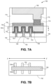
- FIG. 7 A illustrates a cross-sectional view of a non-planar semiconductor device having a ferroelectric or antiferroelectric gate dielectric structure.
- FIG. 7 B illustrates a plan view taken along the a-a′ axis of the semiconductor device of FIG. 7 A , in accordance with an embodiment of the present disclosure.
- a semiconductor structure or device 700 includes a non-planar active region (e.g., a fin structure including protruding fin portion 704 and sub-fin region 705 ) formed from substrate 702 , and within isolation region 706 .
- a gate line 708 is disposed over the protruding portions 704 of the non-planar active region as well as over a portion of the isolation region 706 .
- gate line 708 includes a gate electrode 750 / 799 and a gate dielectric structure 752 / 753 .
- gate line 708 may also include a dielectric cap layer 754 .
- a gate contact 714 , and overlying gate contact via 716 are also seen from this perspective, along with an overlying metal interconnect 760 , all of which are disposed in inter-layer dielectric stacks or layers 770 . Also seen from the perspective of FIG. 7 A , the gate contact 714 is, in one embodiment, disposed over isolation region 706 , but not over the non-planar active regions.
- the gate line 708 is shown as disposed over the protruding fin portions 704 .
- Source and drain regions 704 A and 704 B of the protruding fin portions 704 can be seen from this perspective.
- the source and drain regions 704 A and 704 B are doped portions of original material of the protruding fin portions 704 .
- the material of the protruding fin portions 704 is removed and replaced with another semiconductor material, e.g., by epitaxial deposition. In either case, the source and drain regions 704 A and 704 B may extend below the height of dielectric layer 706 , i.e., into the sub-fin region 705 .
- the semiconductor structure or device 700 is a non-planar device such as, but not limited to, a fin-FET or a tri-gate device.
- a corresponding semiconducting channel region is composed of or is formed in a three-dimensional body.
- the gate electrode and gate electrode materials of gate lines 708 surround at least a top surface and a pair of sidewalls of the three-dimensional body.
- Substrate 702 may be composed of a semiconductor material that can withstand a manufacturing process and in which charge can migrate.
- substrate 702 is a bulk substrate composed of a crystalline silicon, silicon/germanium or germanium layer doped with a charge carrier, such as but not limited to phosphorus, arsenic, antimony, boron, gallium or a combination thereof, to form active region 704 .
- a charge carrier such as but not limited to phosphorus, arsenic, antimony, boron, gallium or a combination thereof.
- the concentration of silicon atoms in bulk substrate 702 is greater than 97%.
- bulk substrate 702 is composed of an epitaxial layer grown atop a distinct crystalline substrate, e.g. a silicon epitaxial layer grown atop a boron-doped bulk silicon mono-crystalline substrate.
- Bulk substrate 702 may alternatively be composed of a group III-V material.
- bulk substrate 702 is composed of a III-V material such as, but not limited to, gallium nitride, gallium phosphide, gallium arsenide, indium phosphide, indium antimonide, indium gallium arsenide, aluminum gallium arsenide, indium gallium phosphide, or a combination thereof.
- bulk substrate 702 is composed of a III-V material and the charge-carrier dopant impurity atoms are ones such as, but not limited to, magnesium, beryllium, zinc, carbon, silicon, germanium, oxygen, sulfur, selenium or tellurium.
- Isolation region 706 may be composed of a material suitable to ultimately electrically isolate, or contribute to the isolation of, portions of a permanent gate structure from an underlying bulk substrate or isolate active regions formed within an underlying bulk substrate, such as isolating fin active regions.
- the isolation region 706 is composed of a dielectric material such as, but not limited to, silicon dioxide, silicon oxy-nitride, silicon nitride, or carbon-doped silicon nitride.
- the gate dielectric structure includes a ferroelectric or antiferroelectric polycrystalline material layer 752 .
- the gate dielectric structure further includes an amorphous oxide layer 753 .
- the ferroelectric or antiferroelectric polycrystalline material layer 752 may consist of a “U”-shaped structure that includes a bottom portion substantially parallel to the surface of the substrate and two sidewall portions that are substantially perpendicular to the top surface of the substrate.
- layer 750 of the gate electrode 750 / 799 is composed of a non-workfunction-setting conductive fill material formed above a workfunction-setting layer 799 .
- the conductive fill material 750 includes a material such as but not limited to, tungsten (W), aluminum (Al), or copper (Cu).
- metals that may be used for the workfunction-setting layer 799 include, but are not limited to, ruthenium, palladium, platinum, cobalt, nickel, and conductive metal oxides, e.g., ruthenium oxide.
- a P-type metal layer will enable the formation of a PMOS gate electrode with a workfunction that is between about 4.9 eV and about 5.2 eV.
- metals that may be used for the workfunction-setting layer 799 include, but are not limited to, hafnium, zirconium, titanium, tantalum, aluminum, alloys of these metals, and carbides of these metals such as hafnium carbide, zirconium carbide, titanium carbide, tantalum carbide, and aluminum carbide.
- An N-type metal layer will enable the formation of an NMOS gate electrode with a workfunction that is between about 3.9 eV and about 4.2 eV.
- the workfunction-setting layer 799 may consist of a “U”-shaped structure that includes a bottom portion substantially parallel to the surface of the substrate and two sidewall portions that are substantially perpendicular to the top surface of the substrate.
- at least one of the metal layers that form the gate electrode may simply be a planar layer that is substantially parallel to the top surface of the substrate and does not include sidewall portions substantially perpendicular to the top surface of the substrate.
- the gate electrode may consist of a combination of U-shaped structures and planar, non-U-shaped structures.
- the gate electrode may consist of one or more U-shaped metal layers formed atop one or more planar, non-U-shaped layers.
- the dielectric cap layer 754 and/or dielectric spacers associated with the gate electrode stacks may be composed of a material suitable to ultimately electrically isolate, or contribute to the isolation of, a permanent gate structure from adjacent or overlying conductive contacts, such as self-aligned contacts.
- the dielectric cap layer 754 and/or dielectric spacers are composed of a dielectric material such as, but not limited to, silicon dioxide, silicon oxy-nitride, silicon nitride, or carbon-doped silicon nitride.
- Gate contact 714 , overlying gate contact via 716 , and/or overlying metal interconnect 760 may be composed of a conductive material.
- one or more of the contacts, interconnects or vias are composed of a metal species.
- the metal species may be a pure metal, such as tungsten, nickel, or cobalt, or may be an alloy such as a metal-metal alloy or a metal-semiconductor alloy (e.g., such as a silicide material).
- one or more of gate contact 714 , overlying gate contact via 716 , or overlying metal interconnect 760 includes a barrier layer and a conductive fill material.
- the barrier layer is a tantalum nitride layer or a titanium nitride layer.
- the conductive fill material is composed of a conductive material such as, but not limited to, Cu, Al, Ti, Zr, Hf, V, Ru, Co, Ni, Pd, Pt, W, Ag, Au or alloys thereof.
- providing structure 700 involves formation of a contact pattern which is essentially perfectly aligned to an existing gate pattern while eliminating the use of a lithographic step with exceedingly tight registration budget.
- this approach enables the use of intrinsically highly selective wet etching (e.g., versus conventionally implemented dry or plasma etching) to generate contact openings.
- a contact pattern is formed by utilizing an existing gate pattern in combination with a contact plug lithography operation.
- the approach enables elimination of the need for an otherwise critical lithography operation to generate a contact pattern, as used in conventional approaches.
- a trench contact grid is not separately patterned, but is rather formed between poly (gate) lines. For example, in one such embodiment, a trench contact grid is formed subsequent to gate grating patterning but prior to gate grating cuts.
- the gate stack structure 708 may be fabricated by a replacement gate process.
- dummy gate material such as polysilicon or silicon nitride pillar material, may be removed and replaced with permanent gate electrode material.
- a permanent gate dielectric layer is also formed in this process, as opposed to being carried through from earlier processing.
- dummy gates are removed by a dry etch or wet etch process.
- dummy gates are composed of polycrystalline silicon or amorphous silicon and are removed with a dry etch process including use of SF 6 .
- dummy gates are composed of polycrystalline silicon or amorphous silicon and are removed with a wet etch process including use of aqueous NH 4 OH or tetramethylammonium hydroxide. In one embodiment, dummy gates are composed of silicon nitride and are removed with a wet etch including aqueous phosphoric acid.
- one or more approaches described herein contemplate essentially a dummy and replacement gate process in combination with a dummy and replacement contact process to arrive at structure 700 .
- the replacement contact process is performed after the replacement gate process to allow high temperature anneal of at least a portion of the permanent gate stack.
- an anneal of at least a portion of the permanent gate structures e.g., after a gate dielectric layer is formed, is performed at a temperature greater than approximately 600 degrees Celsius. The anneal is performed prior to formation of the permanent contacts.
- a semiconductor device has contact structures that contact portions of a gate electrode formed over an active region.
- a gate contact structure such as a via
- one or more embodiments of the present disclosure include first using a gate aligned trench contact process. Such a process may be implemented to form trench contact structures for semiconductor structure fabrication, e.g., for integrated circuit fabrication.
- a trench contact pattern is formed as aligned to an existing gate pattern.
- a conventional process may include patterning of a poly (gate) grid with separate patterning of contact features.
- dummy gates need not ever be formed prior to fabricating gate contacts over active portions of the gate stacks.
- the gate stacks described above may actually be permanent gate stacks as initially formed.
- the processes described herein may be used to fabricate one or a plurality of semiconductor devices.
- the semiconductor devices may be transistors or like devices.
- the semiconductor devices are a metal-oxide semiconductor (MOS) transistors for logic or memory, or are bipolar transistors.
- MOS metal-oxide semiconductor
- the semiconductor devices have a three-dimensional architecture, such as a trigate device, an independently accessed double gate device, or a FIN-FET.
- a trigate device such as a trigate device, an independently accessed double gate device, or a FIN-FET.
- One or more embodiments may be particularly useful for fabricating semiconductor devices at a 10 nanometer (10 nm) or smaller technology node.
- lithographic operations are performed using 193 nm immersion lithography (i193), extreme ultra-violet (EUV) and/or electron beam direct write (EBDW) lithography, or the like.
- a positive tone or a negative tone resist may be used.
- a lithographic mask is a trilayer mask composed of a topographic masking portion, an anti-reflective coating (ARC) layer, and a photoresist layer.
- the topographic masking portion is a carbon hardmask (CHM) layer and the anti-reflective coating layer is a silicon ARC layer.
- Embodiments disclosed herein may be used to manufacture a wide variety of different types of integrated circuits and/or microelectronic devices. Examples of such integrated circuits include, but are not limited to, processors, chipset components, graphics processors, digital signal processors, micro-controllers, and the like. In other embodiments, semiconductor memory may be manufactured. Moreover, the integrated circuits or other microelectronic devices may be used in a wide variety of electronic devices known in the arts. For example, in computer systems (e.g., desktop, laptop, server), cellular phones, personal electronics, etc. The integrated circuits may be coupled with a bus and other components in the systems. For example, a processor may be coupled by one or more buses to a memory, a chipset, etc. Each of the processor, the memory, and the chipset, may potentially be manufactured using the approaches disclosed herein.
- FIG. 8 illustrates a computing device 800 in accordance with one implementation of the disclosure.
- the computing device 800 houses a board 802 .
- the board 802 may include a number of components, including but not limited to a processor 804 and at least one communication chip 806 .
- the processor 804 is physically and electrically coupled to the board 802 .
- the at least one communication chip 806 is also physically and electrically coupled to the board 802 .
- the communication chip 806 is part of the processor 804 .
- computing device 800 may include other components that may or may not be physically and electrically coupled to the board 802 .
- these other components include, but are not limited to, volatile memory (e.g., DRAM), non-volatile memory (e.g., ROM), flash memory, a graphics processor, a digital signal processor, a crypto processor, a chipset, an antenna, a display, a touchscreen display, a touchscreen controller, a battery, an audio codec, a video codec, a power amplifier, a global positioning system (GPS) device, a compass, an accelerometer, a gyroscope, a speaker, a camera, and a mass storage device (such as hard disk drive, compact disk (CD), digital versatile disk (DVD), and so forth).
- volatile memory e.g., DRAM
- non-volatile memory e.g., ROM
- flash memory e.g., a graphics processor, a digital signal processor, a crypto processor, a chipset, an
- the communication chip 806 enables wireless communications for the transfer of data to and from the computing device 800 .
- the term “wireless” and its derivatives may be used to describe circuits, devices, systems, methods, techniques, communications channels, etc., that may communicate data through the use of modulated electromagnetic radiation through a non-solid medium. The term does not imply that the associated devices do not contain any wires, although in some embodiments they might not.
- the communication chip 806 may implement any of a number of wireless standards or protocols, including but not limited to Wi-Fi (IEEE 802.11 family), WiMAX (IEEE 802.16 family), IEEE 802.20, long term evolution (LTE), Ev-DO, HSPA+, HSDPA+, HSUPA+, EDGE, GSM, GPRS, CDMA, TDMA, DECT, Bluetooth, derivatives thereof, as well as any other wireless protocols that are designated as 3G, 4G, 5G, and beyond.
- the computing device 800 may include a plurality of communication chips 806 .
- a first communication chip 806 may be dedicated to shorter range wireless communications such as Wi-Fi and Bluetooth and a second communication chip 806 may be dedicated to longer range wireless communications such as GPS, EDGE, GPRS, CDMA, WiMAX, LTE, Ev-DO, and others.
- the processor 804 of the computing device 800 includes an integrated circuit die packaged within the processor 804 .
- the integrated circuit die of the processor includes one or more field effect transistors having a ferroelectric or antiferroelectric gate dielectric structure, in accordance with implementations of embodiments of the disclosure.
- the term “processor” may refer to any device or portion of a device that processes electronic data from registers and/or memory to transform that electronic data into other electronic data that may be stored in registers and/or memory.
- the communication chip 806 also includes an integrated circuit die packaged within the communication chip 806 .
- the integrated circuit die of the communication chip includes one or more field effect transistors having a ferroelectric or antiferroelectric gate dielectric structure, in accordance with implementations of embodiments of the disclosure.
- another component housed within the computing device 800 may contain an integrated circuit die that includes one or more field effect transistors having a ferroelectric or antiferroelectric gate dielectric structure, in accordance with implementations of embodiments of the disclosure.
- the computing device 800 may be a laptop, a netbook, a notebook, an ultrabook, a smartphone, a tablet, a personal digital assistant (PDA), an ultra mobile PC, a mobile phone, a desktop computer, a server, a printer, a scanner, a monitor, a set-top box, an entertainment control unit, a digital camera, a portable music player, or a digital video recorder.
- the computing device 800 may be any other electronic device that processes data.
- FIG. 9 illustrates an interposer 900 that includes one or more embodiments of the disclosure.
- the interposer 900 is an intervening substrate used to bridge a first substrate 902 to a second substrate 904 .
- the first substrate 902 may be, for instance, an integrated circuit die.
- the second substrate 904 may be, for instance, a memory module, a computer motherboard, or another integrated circuit die.
- the purpose of an interposer 900 is to spread a connection to a wider pitch or to reroute a connection to a different connection.
- an interposer 900 may couple an integrated circuit die to a ball grid array (BGA) 906 that can subsequently be coupled to the second substrate 904 .
- BGA ball grid array
- first and second substrates 902 / 904 are attached to opposing sides of the interposer 900 . In other embodiments, the first and second substrates 902 / 904 are attached to the same side of the interposer 900 . And in further embodiments, three or more substrates are interconnected by way of the interposer 900 .
- the interposer 900 may be formed of an epoxy resin, a fiberglass-reinforced epoxy resin, a ceramic material, or a polymer material such as polyimide.
- the interposer may be formed of alternate rigid or flexible materials that may include the same materials described above for use in a semiconductor substrate, such as silicon, germanium, and other group III-V and group IV materials.
- the interposer may include metal interconnects 908 and vias 910 , including but not limited to through-silicon vias (TSVs) 912 .
- the interposer 900 may further include embedded devices 914 , including both passive and active devices. Such devices include, but are not limited to, capacitors, decoupling capacitors, resistors, inductors, fuses, diodes, transformers, sensors, and electrostatic discharge (ESD) devices. More complex devices such as radio-frequency (RF) devices, power amplifiers, power management devices, antennas, arrays, sensors, and MEMS devices may also be formed on the interposer 900 .
- RF radio-frequency
- apparatuses or processes disclosed herein may be used in the fabrication of interposer 900 .
- embodiments described herein include field effect transistors having a ferroelectric or antiferroelectric gate dielectric structure.
- An integrated circuit structure includes a semiconductor channel structure includes a monocrystalline material.
- a gate dielectric is over the semiconductor channel structure.
- the gate dielectric includes a ferroelectric or antiferroelectric polycrystalline material layer.
- a gate electrode has a conductive layer on the ferroelectric or antiferroelectric polycrystalline material layer, the conductive layer including a metal.
- a first source or drain structure is at a first side of the gate electrode.
- a second source or drain structure is at a second side of the gate electrode opposite the first side.
- Example embodiment 2 The integrated circuit structure of example embodiment 1, wherein the ferroelectric or antiferroelectric polycrystalline material layer is a ferroelectric polycrystalline material layer.
- Example embodiment 3 The integrated circuit structure of example embodiment 2, wherein the ferroelectric polycrystalline material layer is an oxide including Zr and Hf with a Zr:Hf ratio of 50:50 or greater in Zr.
- Example embodiment 4 The integrated circuit structure of example embodiment 2 or 3, wherein the ferroelectric polycrystalline material layer has at least 80% orthorhombic crystallinity.
- Example embodiment 5 The integrated circuit structure of example embodiment 1, wherein the ferroelectric or antiferroelectric polycrystalline material layer is an antiferroelectric polycrystalline material layer.
- Example embodiment 6 The integrated circuit structure of example embodiment 5, wherein the antiferroelectric polycrystalline material layer is an oxide including Zr and Hf with a Zr:Hf ratio of 80:20 or greater in Zr.
- Example embodiment 7 The integrated circuit structure of example embodiment 5 or 6, wherein the antiferroelectric polycrystalline material layer has at least 80% tetragonal crystallinity.
- Example embodiment 8 The integrated circuit structure of example embodiment 1, 2, 3, 4, 5, 6 or 7, wherein the gate dielectric further includes an amorphous oxide layer between the ferroelectric or antiferroelectric polycrystalline material layer and the semiconductor channel structure.
- An integrated circuit structure includes a semiconductor channel structure includes a monocrystalline material.
- a gate dielectric is over the semiconductor channel structure.
- the gate dielectric includes a ferroelectric or antiferroelectric polycrystalline material layer.
- a gate electrode has a conductive layer on the ferroelectric or antiferroelectric polycrystalline material layer, the conductive layer including a metal.
- a first source or drain structure is at a first side of the gate electrode.
- a first dielectric spacer is between the first source or drain structure and the first side of the gate electrode.
- a second source or drain structure is at a second side of the gate electrode opposite the first side.
- a second dielectric spacer between the second source or drain structure and the second side of the gate electrode.
- Example embodiment 10 The integrated circuit structure of example embodiment 9, wherein the ferroelectric or antiferroelectric polycrystalline material layer extends along the first dielectric spacer and the second dielectric spacer.
- Example embodiment 11 The integrated circuit structure of example embodiment 9, wherein the ferroelectric or antiferroelectric polycrystalline material layer extends beneath the first dielectric spacer and the second dielectric spacer.
- Example embodiment 12 The integrated circuit structure of example embodiment 9, 10 or 11, wherein the ferroelectric or antiferroelectric polycrystalline material layer is a ferroelectric polycrystalline material layer.
- Example embodiment 13 The integrated circuit structure of example embodiment 12, wherein the ferroelectric polycrystalline material layer is an oxide including Zr and Hf with a Zr:Hf ratio of 50:50 or greater in Zr.
- Example embodiment 14 The integrated circuit structure of example embodiment 12 or 13, wherein the ferroelectric polycrystalline material layer has at least 80% orthorhombic crystallinity.
- Example embodiment 15 The integrated circuit structure of example embodiment 9, 10 or 11, wherein the ferroelectric or antiferroelectric polycrystalline material layer is an antiferroelectric polycrystalline material layer.
- Example embodiment 16 The integrated circuit structure of example embodiment 15, wherein the antiferroelectric polycrystalline material layer is an oxide including Zr and Hf with a Zr:Hf ratio of 80:20 or greater in Zr.
- Example embodiment 17 The integrated circuit structure of example embodiment 15 or 16, wherein the antiferroelectric polycrystalline material layer has at least 80% tetragonal crystallinity.
- Example embodiment 18 The integrated circuit structure of example embodiment 9, 10, 11, 12, 13, 14, 15, 16 or 17, wherein the gate dielectric further includes an amorphous oxide layer between the ferroelectric or antiferroelectric polycrystalline material layer and the semiconductor channel structure.
- An integrated circuit structure includes a semiconductor channel structure including a monocrystalline material.
- a gate dielectric is over the semiconductor channel structure.
- a gate electrode is on the gate dielectric.
- a first source or drain structure is at a first side of the gate electrode.
- a first dielectric spacer is between the first source or drain structure and the first side of the gate electrode.
- a second source or drain structure is at a second side of the gate electrode opposite the first side.
- a second dielectric spacer is between the second source or drain structure and the second side of the gate electrode.
- a ferroelectric or antiferroelectric polycrystalline material layer is beneath the first and second dielectric spacers and adjacent the gate dielectric.
- Example embodiment 20 The integrated circuit structure of example embodiment 19, wherein the ferroelectric or antiferroelectric polycrystalline material layer is an oxide including Zr and Hf, and wherein the gate dielectric includes a layer of amorphous hafnium oxide.
- Example embodiment 21 The integrated circuit structure of example embodiment 19 or 20, wherein the ferroelectric or antiferroelectric polycrystalline material layer has at least 80% orthorhombic crystallinity.
- Example embodiment 22 The integrated circuit structure of example embodiment 19 or 20, wherein the ferroelectric or antiferroelectric polycrystalline material layer has at least 80% tetragonal crystallinity.
Landscapes
- Semiconductor Memories (AREA)
- Thin Film Transistor (AREA)
- Insulated Gate Type Field-Effect Transistor (AREA)
Abstract
Description
Claims (19)
Applications Claiming Priority (1)
| Application Number | Priority Date | Filing Date | Title |
|---|---|---|---|
| PCT/US2017/054164 WO2019066875A1 (en) | 2017-09-28 | 2017-09-28 | Field effect transistors having ferroelectric or antiferroelectric gate dielectric structure |
Publications (2)
| Publication Number | Publication Date |
|---|---|
| US20200321446A1 US20200321446A1 (en) | 2020-10-08 |
| US11735652B2 true US11735652B2 (en) | 2023-08-22 |
Family
ID=65902259
Family Applications (1)
| Application Number | Title | Priority Date | Filing Date |
|---|---|---|---|
| US16/635,739 Active 2038-02-15 US11735652B2 (en) | 2017-09-28 | 2017-09-28 | Field effect transistors having ferroelectric or antiferroelectric gate dielectric structure |
Country Status (3)
| Country | Link |
|---|---|
| US (1) | US11735652B2 (en) |
| EP (1) | EP3688815A4 (en) |
| WO (1) | WO2019066875A1 (en) |
Families Citing this family (5)
| Publication number | Priority date | Publication date | Assignee | Title |
|---|---|---|---|---|
| US11335806B2 (en) | 2020-08-11 | 2022-05-17 | Taiwan Semiconductor Manufacturing Co., Ltd. | Semiconductor device structure and method for forming the same |
| WO2022040702A2 (en) * | 2020-08-21 | 2022-02-24 | Rutgers, The State University Of New Jersey | Multifunctional mzo-based negative capacitance thin film transistor on glass or flexible substrates |
| US20220199758A1 (en) * | 2020-12-23 | 2022-06-23 | Intel Corporation | Carbon electrodes for ferroelectric capacitors |
| US20220199756A1 (en) * | 2020-12-23 | 2022-06-23 | Intel Corporation | Metal insulator metal (mim) capacitor or backend transistor having epitaxial oxide |
| US12002860B2 (en) * | 2021-08-13 | 2024-06-04 | Taiwan Semiconductor Manufacturing Company, Ltd. | Semiconductor device and fabrication method thereof |
Citations (7)
| Publication number | Priority date | Publication date | Assignee | Title |
|---|---|---|---|---|
| WO2003030243A1 (en) | 2001-10-02 | 2003-04-10 | Asm America, Inc. | Incorporation of nitrogen into high k dielectric film |
| US20040141357A1 (en) * | 2002-09-19 | 2004-07-22 | Klaus Dimmler | Ferroelectric transistor for storing two data bits |
| US20080076214A1 (en) | 2006-09-25 | 2008-03-27 | Jin-Ping Han | Semiconductor device and method of making same |
| US20120070955A1 (en) | 2004-09-01 | 2012-03-22 | Micron Technology, Inc. | Methods of Forming Conductive Contacts to Source/Drain Regions and Methods of Forming Local Interconnects |
| US20160247932A1 (en) * | 2013-07-25 | 2016-08-25 | National Institute Of Advanced Industrial Science And Technology | Ferroelectric device and meethod for manufacturing same |
| US20170141235A1 (en) * | 2015-11-16 | 2017-05-18 | Taiwan Semiconductor Manufacturing Company, Ltd. | Negative Capacitance Field Effect Transistor With Charged Dielectric Material |
| US20170358684A1 (en) * | 2016-06-08 | 2017-12-14 | United Microelectronics Corp. | Semiconductor device |
Family Cites Families (3)
| Publication number | Priority date | Publication date | Assignee | Title |
|---|---|---|---|---|
| US10242989B2 (en) * | 2014-05-20 | 2019-03-26 | Micron Technology, Inc. | Polar, chiral, and non-centro-symmetric ferroelectric materials, memory cells including such materials, and related devices and methods |
| US10153155B2 (en) * | 2015-10-09 | 2018-12-11 | University Of Florida Research Foundation, Incorporated | Doped ferroelectric hafnium oxide film devices |
| DE102015015854B4 (en) * | 2015-12-03 | 2021-01-28 | Namlab Ggmbh | Integrated circuit with a ferroelectric memory cell and use of the integrated circuit |
-
2017
- 2017-09-28 WO PCT/US2017/054164 patent/WO2019066875A1/en not_active Ceased
- 2017-09-28 US US16/635,739 patent/US11735652B2/en active Active
- 2017-09-28 EP EP17927533.4A patent/EP3688815A4/en not_active Ceased
Patent Citations (8)
| Publication number | Priority date | Publication date | Assignee | Title |
|---|---|---|---|---|
| WO2003030243A1 (en) | 2001-10-02 | 2003-04-10 | Asm America, Inc. | Incorporation of nitrogen into high k dielectric film |
| JP2005505920A (en) | 2001-10-02 | 2005-02-24 | エーエスエム アメリカ インコーポレイテッド | Nitrogen incorporation into high-k dielectric films |
| US20040141357A1 (en) * | 2002-09-19 | 2004-07-22 | Klaus Dimmler | Ferroelectric transistor for storing two data bits |
| US20120070955A1 (en) | 2004-09-01 | 2012-03-22 | Micron Technology, Inc. | Methods of Forming Conductive Contacts to Source/Drain Regions and Methods of Forming Local Interconnects |
| US20080076214A1 (en) | 2006-09-25 | 2008-03-27 | Jin-Ping Han | Semiconductor device and method of making same |
| US20160247932A1 (en) * | 2013-07-25 | 2016-08-25 | National Institute Of Advanced Industrial Science And Technology | Ferroelectric device and meethod for manufacturing same |
| US20170141235A1 (en) * | 2015-11-16 | 2017-05-18 | Taiwan Semiconductor Manufacturing Company, Ltd. | Negative Capacitance Field Effect Transistor With Charged Dielectric Material |
| US20170358684A1 (en) * | 2016-06-08 | 2017-12-14 | United Microelectronics Corp. | Semiconductor device |
Non-Patent Citations (12)
| Title |
|---|
| "Snow ES et al.: ""A Metal/Oxide Tunnelling Transistor"", Semiconductor Science Technology, IOP Publishing Ltd, GB, vol. 13, No. SA, Aug. 1, 1998 (Aug. 1, 1998), pp. A75-A78, XP000768868, ISSN: 0268-1242, DOI: 10.1088/0268-1242/13/SA/023". |
| Anna Chernikova et al.: "Ultrathin Hf 0.5 Zr 0.5 0 2 Ferroelectric Films on Si", ACS Applied Materials & Interfaces, vol. 8, No. 11, Mar. 14, 2016 (Mar. 14, 2016), pp. 7232-7237, XP055459026, US ISSN: 1944-8244. |
| ANNA CHERNIKOVA, MAKSIM KOZODAEV, ANDREI MARKEEV, DMITRII NEGROV, MAKSIM SPIRIDONOV, SERGEI ZARUBIN, OHHEUM BAK, PRATYUSH BURAGOHA: "Ultrathin Hf 0.5 Zr 0.5 O 2 Ferroelectric Films on Si", APPLIED MATERIALS & INTERFACES, AMERICAN CHEMICAL SOCIETY, US, vol. 8, no. 11, 23 March 2016 (2016-03-23), US , pages 7232 - 7237, XP055459026, ISSN: 1944-8244, DOI: 10.1021/acsami.5b11653 |
| International Search Report and Written Opinion for International Patent Application No. PCT/US2017/054164 dated Apr. 9, 2020, 10 pgs. |
| International Search Report and Written Opinion for International Patent Application No. PCT/US2017/054164 dated May 29, 2018, 13 pgs. |
| J. ROBERTSON: "High dielectric constant oxides", THE EUROPEAN PHYSICAL JOURNAL APPLIED PHYSICS, vol. 28, no. 3, 1 December 2004 (2004-12-01), pages 265 - 291, XP055054404, ISSN: 12860042, DOI: 10.1051/epjap:2004206 |
| J. Robertson: "High dielectric constant oxides", The European Physical Journal Applied Physics, vol. 28, No. 3, Dec. 1, 2004 (Dec. 1, 2004), pp. 265-291, XP055054404, ISSN: 1286-0042. |
| Migita et al. "Polarization switching behavior of Hf—Zr—O ferroelectric ultrathin films studied through coercive field characteristics," Japanese Journal of Applied Physics 57, 04FB01, 2018 (Year: 2018). * |
| Muller et al., ."Ferroelectricity in Simple Binary ZrO2 and HfO2," Nano Lett. , 12, pp. 4318-4323, 2012 (Year: 2012). * |
| Office Action for European Patent Application No. 17927533.4, dated Jul. 5, 2022, 6 pgs. |
| Search Report from European Patent Application No. 17927533.4, dated Mar. 16, 2021, 7 pgs. |
| SNOW E. S., ET AL.: "A METAL/OXIDE TUNNELLING TRANSISTOR.", SEMICONDUCTOR SCIENCE TECHNOLOGY, IOP PUBLISHING LTD, GB, vol. 13., no. 08A., 1 August 1998 (1998-08-01), GB , pages A75 - A78., XP000768868, ISSN: 0268-1242, DOI: 10.1088/0268-1242/13/8A/023 |
Also Published As
| Publication number | Publication date |
|---|---|
| WO2019066875A1 (en) | 2019-04-04 |
| EP3688815A1 (en) | 2020-08-05 |
| EP3688815A4 (en) | 2021-04-14 |
| US20200321446A1 (en) | 2020-10-08 |
Similar Documents
| Publication | Publication Date | Title |
|---|---|---|
| US12125917B2 (en) | Thin film transistors having double gates | |
| US11380797B2 (en) | Thin film core-shell fin and nanowire transistors | |
| US12328927B2 (en) | Low resistance and reduced reactivity approaches for fabricating contacts and the resulting structures | |
| US12402387B2 (en) | Integrated circuit structures including a titanium silicide material | |
| US11984506B2 (en) | Field effect transistor having a gate dielectric with a dipole layer and having a gate stressor layer | |
| US12119387B2 (en) | Low resistance approaches for fabricating contacts and the resulting structures | |
| US20220246646A1 (en) | Thin film tunnel field effect transistors having relatively increased width | |
| US12224239B2 (en) | Internal node jumper for memory bit cells | |
| US11749733B2 (en) | FIN shaping using templates and integrated circuit structures resulting therefrom | |
| US11735652B2 (en) | Field effect transistors having ferroelectric or antiferroelectric gate dielectric structure | |
| US20200350412A1 (en) | Thin film transistors having alloying source or drain metals | |
| WO2018236357A1 (en) | Thin film transistors having relatively increased width | |
| US11476164B2 (en) | Integrated circuit structures having differentiated workfunction layers | |
| US12080643B2 (en) | Integrated circuit structures having differentiated interconnect lines in a same dielectric layer | |
| US20210090997A1 (en) | Self-aligned patterning with colored blocking and structures resulting therefrom | |
| US11063151B2 (en) | Metal chemical vapor deposition approaches for fabricating wrap-around contacts and resulting structures | |
| US20260096181A1 (en) | Conformal approaches for fabricating contacts and the resulting structures | |
| US12432976B2 (en) | Thin film transistors having strain-inducing structures integrated with 2D channel materials |
Legal Events
| Date | Code | Title | Description |
|---|---|---|---|
| FEPP | Fee payment procedure |
Free format text: ENTITY STATUS SET TO UNDISCOUNTED (ORIGINAL EVENT CODE: BIG.); ENTITY STATUS OF PATENT OWNER: LARGE ENTITY |
|
| STPP | Information on status: patent application and granting procedure in general |
Free format text: DOCKETED NEW CASE - READY FOR EXAMINATION |
|
| STPP | Information on status: patent application and granting procedure in general |
Free format text: NON FINAL ACTION MAILED |
|
| STPP | Information on status: patent application and granting procedure in general |
Free format text: RESPONSE TO NON-FINAL OFFICE ACTION ENTERED AND FORWARDED TO EXAMINER |
|
| STPP | Information on status: patent application and granting procedure in general |
Free format text: FINAL REJECTION MAILED |
|
| STPP | Information on status: patent application and granting procedure in general |
Free format text: RESPONSE AFTER FINAL ACTION FORWARDED TO EXAMINER |
|
| STPP | Information on status: patent application and granting procedure in general |
Free format text: ADVISORY ACTION MAILED |
|
| STPP | Information on status: patent application and granting procedure in general |
Free format text: DOCKETED NEW CASE - READY FOR EXAMINATION |
|
| STPP | Information on status: patent application and granting procedure in general |
Free format text: NON FINAL ACTION MAILED |
|
| STPP | Information on status: patent application and granting procedure in general |
Free format text: RESPONSE TO NON-FINAL OFFICE ACTION ENTERED AND FORWARDED TO EXAMINER |
|
| AS | Assignment |
Owner name: INTEL CORPORATION, CALIFORNIA Free format text: ASSIGNMENT OF ASSIGNORS INTEREST;ASSIGNORS:KIM, SEIYON;AVCI, UYGAR E.;HOWARD, JOSHUA M.;AND OTHERS;SIGNING DATES FROM 20171114 TO 20171130;REEL/FRAME:063437/0625 |
|
| STPP | Information on status: patent application and granting procedure in general |
Free format text: PUBLICATIONS -- ISSUE FEE PAYMENT RECEIVED |
|
| STCF | Information on status: patent grant |
Free format text: PATENTED CASE |