US11735113B2 - Pixel driving circuit, method of driving the same and display device - Google Patents
Pixel driving circuit, method of driving the same and display device Download PDFInfo
- Publication number
- US11735113B2 US11735113B2 US17/639,245 US202117639245A US11735113B2 US 11735113 B2 US11735113 B2 US 11735113B2 US 202117639245 A US202117639245 A US 202117639245A US 11735113 B2 US11735113 B2 US 11735113B2
- Authority
- US
- United States
- Prior art keywords
- transistor
- electrode
- control
- sub
- circuit
- Prior art date
- Legal status (The legal status is an assumption and is not a legal conclusion. Google has not performed a legal analysis and makes no representation as to the accuracy of the status listed.)
- Active
Links
- 238000000034 method Methods 0.000 title claims abstract description 29
- 239000003990 capacitor Substances 0.000 claims abstract description 72
- 230000001808 coupling effect Effects 0.000 claims description 6
- 230000008878 coupling Effects 0.000 claims description 4
- 238000010168 coupling process Methods 0.000 claims description 4
- 238000005859 coupling reaction Methods 0.000 claims description 4
- 238000010586 diagram Methods 0.000 description 16
- 230000008569 process Effects 0.000 description 9
- 230000000694 effects Effects 0.000 description 5
- 239000000758 substrate Substances 0.000 description 5
- 229920001621 AMOLED Polymers 0.000 description 4
- 230000008859 change Effects 0.000 description 4
- 206010047571 Visual impairment Diseases 0.000 description 3
- 230000002159 abnormal effect Effects 0.000 description 3
- 230000009286 beneficial effect Effects 0.000 description 3
- 239000002346 layers by function Substances 0.000 description 2
- 230000004048 modification Effects 0.000 description 2
- 238000012986 modification Methods 0.000 description 2
- 229920006395 saturated elastomer Polymers 0.000 description 2
- 230000009471 action Effects 0.000 description 1
- -1 area Substances 0.000 description 1
- 238000005516 engineering process Methods 0.000 description 1
- 238000007667 floating Methods 0.000 description 1
- 239000010410 layer Substances 0.000 description 1
- 238000004519 manufacturing process Methods 0.000 description 1
- 239000000463 material Substances 0.000 description 1
- 230000002093 peripheral effect Effects 0.000 description 1
- 230000000750 progressive effect Effects 0.000 description 1
- 230000004044 response Effects 0.000 description 1
Images


Classifications
-
- G—PHYSICS
- G09—EDUCATION; CRYPTOGRAPHY; DISPLAY; ADVERTISING; SEALS
- G09G—ARRANGEMENTS OR CIRCUITS FOR CONTROL OF INDICATING DEVICES USING STATIC MEANS TO PRESENT VARIABLE INFORMATION
- G09G3/00—Control arrangements or circuits, of interest only in connection with visual indicators other than cathode-ray tubes
- G09G3/20—Control arrangements or circuits, of interest only in connection with visual indicators other than cathode-ray tubes for presentation of an assembly of a number of characters, e.g. a page, by composing the assembly by combination of individual elements arranged in a matrix no fixed position being assigned to or needed to be assigned to the individual characters or partial characters
- G09G3/22—Control arrangements or circuits, of interest only in connection with visual indicators other than cathode-ray tubes for presentation of an assembly of a number of characters, e.g. a page, by composing the assembly by combination of individual elements arranged in a matrix no fixed position being assigned to or needed to be assigned to the individual characters or partial characters using controlled light sources
- G09G3/30—Control arrangements or circuits, of interest only in connection with visual indicators other than cathode-ray tubes for presentation of an assembly of a number of characters, e.g. a page, by composing the assembly by combination of individual elements arranged in a matrix no fixed position being assigned to or needed to be assigned to the individual characters or partial characters using controlled light sources using electroluminescent panels
- G09G3/32—Control arrangements or circuits, of interest only in connection with visual indicators other than cathode-ray tubes for presentation of an assembly of a number of characters, e.g. a page, by composing the assembly by combination of individual elements arranged in a matrix no fixed position being assigned to or needed to be assigned to the individual characters or partial characters using controlled light sources using electroluminescent panels semiconductive, e.g. using light-emitting diodes [LED]
- G09G3/3208—Control arrangements or circuits, of interest only in connection with visual indicators other than cathode-ray tubes for presentation of an assembly of a number of characters, e.g. a page, by composing the assembly by combination of individual elements arranged in a matrix no fixed position being assigned to or needed to be assigned to the individual characters or partial characters using controlled light sources using electroluminescent panels semiconductive, e.g. using light-emitting diodes [LED] organic, e.g. using organic light-emitting diodes [OLED]
- G09G3/3225—Control arrangements or circuits, of interest only in connection with visual indicators other than cathode-ray tubes for presentation of an assembly of a number of characters, e.g. a page, by composing the assembly by combination of individual elements arranged in a matrix no fixed position being assigned to or needed to be assigned to the individual characters or partial characters using controlled light sources using electroluminescent panels semiconductive, e.g. using light-emitting diodes [LED] organic, e.g. using organic light-emitting diodes [OLED] using an active matrix
- G09G3/3258—Control arrangements or circuits, of interest only in connection with visual indicators other than cathode-ray tubes for presentation of an assembly of a number of characters, e.g. a page, by composing the assembly by combination of individual elements arranged in a matrix no fixed position being assigned to or needed to be assigned to the individual characters or partial characters using controlled light sources using electroluminescent panels semiconductive, e.g. using light-emitting diodes [LED] organic, e.g. using organic light-emitting diodes [OLED] using an active matrix with pixel circuitry controlling the voltage across the light-emitting element
-
- G—PHYSICS
- G09—EDUCATION; CRYPTOGRAPHY; DISPLAY; ADVERTISING; SEALS
- G09G—ARRANGEMENTS OR CIRCUITS FOR CONTROL OF INDICATING DEVICES USING STATIC MEANS TO PRESENT VARIABLE INFORMATION
- G09G3/00—Control arrangements or circuits, of interest only in connection with visual indicators other than cathode-ray tubes
- G09G3/20—Control arrangements or circuits, of interest only in connection with visual indicators other than cathode-ray tubes for presentation of an assembly of a number of characters, e.g. a page, by composing the assembly by combination of individual elements arranged in a matrix no fixed position being assigned to or needed to be assigned to the individual characters or partial characters
- G09G3/22—Control arrangements or circuits, of interest only in connection with visual indicators other than cathode-ray tubes for presentation of an assembly of a number of characters, e.g. a page, by composing the assembly by combination of individual elements arranged in a matrix no fixed position being assigned to or needed to be assigned to the individual characters or partial characters using controlled light sources
- G09G3/30—Control arrangements or circuits, of interest only in connection with visual indicators other than cathode-ray tubes for presentation of an assembly of a number of characters, e.g. a page, by composing the assembly by combination of individual elements arranged in a matrix no fixed position being assigned to or needed to be assigned to the individual characters or partial characters using controlled light sources using electroluminescent panels
- G09G3/32—Control arrangements or circuits, of interest only in connection with visual indicators other than cathode-ray tubes for presentation of an assembly of a number of characters, e.g. a page, by composing the assembly by combination of individual elements arranged in a matrix no fixed position being assigned to or needed to be assigned to the individual characters or partial characters using controlled light sources using electroluminescent panels semiconductive, e.g. using light-emitting diodes [LED]
- G09G3/3208—Control arrangements or circuits, of interest only in connection with visual indicators other than cathode-ray tubes for presentation of an assembly of a number of characters, e.g. a page, by composing the assembly by combination of individual elements arranged in a matrix no fixed position being assigned to or needed to be assigned to the individual characters or partial characters using controlled light sources using electroluminescent panels semiconductive, e.g. using light-emitting diodes [LED] organic, e.g. using organic light-emitting diodes [OLED]
- G09G3/3225—Control arrangements or circuits, of interest only in connection with visual indicators other than cathode-ray tubes for presentation of an assembly of a number of characters, e.g. a page, by composing the assembly by combination of individual elements arranged in a matrix no fixed position being assigned to or needed to be assigned to the individual characters or partial characters using controlled light sources using electroluminescent panels semiconductive, e.g. using light-emitting diodes [LED] organic, e.g. using organic light-emitting diodes [OLED] using an active matrix
- G09G3/3233—Control arrangements or circuits, of interest only in connection with visual indicators other than cathode-ray tubes for presentation of an assembly of a number of characters, e.g. a page, by composing the assembly by combination of individual elements arranged in a matrix no fixed position being assigned to or needed to be assigned to the individual characters or partial characters using controlled light sources using electroluminescent panels semiconductive, e.g. using light-emitting diodes [LED] organic, e.g. using organic light-emitting diodes [OLED] using an active matrix with pixel circuitry controlling the current through the light-emitting element
- G09G3/3241—Control arrangements or circuits, of interest only in connection with visual indicators other than cathode-ray tubes for presentation of an assembly of a number of characters, e.g. a page, by composing the assembly by combination of individual elements arranged in a matrix no fixed position being assigned to or needed to be assigned to the individual characters or partial characters using controlled light sources using electroluminescent panels semiconductive, e.g. using light-emitting diodes [LED] organic, e.g. using organic light-emitting diodes [OLED] using an active matrix with pixel circuitry controlling the current through the light-emitting element the current through the light-emitting element being set using a data current provided by the data driver, e.g. by using a two-transistor current mirror
-
- G—PHYSICS
- G09—EDUCATION; CRYPTOGRAPHY; DISPLAY; ADVERTISING; SEALS
- G09G—ARRANGEMENTS OR CIRCUITS FOR CONTROL OF INDICATING DEVICES USING STATIC MEANS TO PRESENT VARIABLE INFORMATION
- G09G2300/00—Aspects of the constitution of display devices
- G09G2300/04—Structural and physical details of display devices
- G09G2300/0421—Structural details of the set of electrodes
- G09G2300/0426—Layout of electrodes and connections
-
- G—PHYSICS
- G09—EDUCATION; CRYPTOGRAPHY; DISPLAY; ADVERTISING; SEALS
- G09G—ARRANGEMENTS OR CIRCUITS FOR CONTROL OF INDICATING DEVICES USING STATIC MEANS TO PRESENT VARIABLE INFORMATION
- G09G2300/00—Aspects of the constitution of display devices
- G09G2300/08—Active matrix structure, i.e. with use of active elements, inclusive of non-linear two terminal elements, in the pixels together with light emitting or modulating elements
- G09G2300/0809—Several active elements per pixel in active matrix panels
- G09G2300/0819—Several active elements per pixel in active matrix panels used for counteracting undesired variations, e.g. feedback or autozeroing
-
- G—PHYSICS
- G09—EDUCATION; CRYPTOGRAPHY; DISPLAY; ADVERTISING; SEALS
- G09G—ARRANGEMENTS OR CIRCUITS FOR CONTROL OF INDICATING DEVICES USING STATIC MEANS TO PRESENT VARIABLE INFORMATION
- G09G2300/00—Aspects of the constitution of display devices
- G09G2300/08—Active matrix structure, i.e. with use of active elements, inclusive of non-linear two terminal elements, in the pixels together with light emitting or modulating elements
- G09G2300/0809—Several active elements per pixel in active matrix panels
- G09G2300/0842—Several active elements per pixel in active matrix panels forming a memory circuit, e.g. a dynamic memory with one capacitor
- G09G2300/0852—Several active elements per pixel in active matrix panels forming a memory circuit, e.g. a dynamic memory with one capacitor being a dynamic memory with more than one capacitor
-
- G—PHYSICS
- G09—EDUCATION; CRYPTOGRAPHY; DISPLAY; ADVERTISING; SEALS
- G09G—ARRANGEMENTS OR CIRCUITS FOR CONTROL OF INDICATING DEVICES USING STATIC MEANS TO PRESENT VARIABLE INFORMATION
- G09G2310/00—Command of the display device
- G09G2310/02—Addressing, scanning or driving the display screen or processing steps related thereto
- G09G2310/0202—Addressing of scan or signal lines
- G09G2310/0216—Interleaved control phases for different scan lines in the same sub-field, e.g. initialization, addressing and sustaining in plasma displays that are not simultaneous for all scan lines
-
- G—PHYSICS
- G09—EDUCATION; CRYPTOGRAPHY; DISPLAY; ADVERTISING; SEALS
- G09G—ARRANGEMENTS OR CIRCUITS FOR CONTROL OF INDICATING DEVICES USING STATIC MEANS TO PRESENT VARIABLE INFORMATION
- G09G2310/00—Command of the display device
- G09G2310/02—Addressing, scanning or driving the display screen or processing steps related thereto
- G09G2310/0243—Details of the generation of driving signals
- G09G2310/0251—Precharge or discharge of pixel before applying new pixel voltage
-
- G—PHYSICS
- G09—EDUCATION; CRYPTOGRAPHY; DISPLAY; ADVERTISING; SEALS
- G09G—ARRANGEMENTS OR CIRCUITS FOR CONTROL OF INDICATING DEVICES USING STATIC MEANS TO PRESENT VARIABLE INFORMATION
- G09G2310/00—Command of the display device
- G09G2310/06—Details of flat display driving waveforms
- G09G2310/061—Details of flat display driving waveforms for resetting or blanking
-
- G—PHYSICS
- G09—EDUCATION; CRYPTOGRAPHY; DISPLAY; ADVERTISING; SEALS
- G09G—ARRANGEMENTS OR CIRCUITS FOR CONTROL OF INDICATING DEVICES USING STATIC MEANS TO PRESENT VARIABLE INFORMATION
- G09G2320/00—Control of display operating conditions
- G09G2320/02—Improving the quality of display appearance
- G09G2320/0204—Compensation of DC component across the pixels in flat panels
-
- G—PHYSICS
- G09—EDUCATION; CRYPTOGRAPHY; DISPLAY; ADVERTISING; SEALS
- G09G—ARRANGEMENTS OR CIRCUITS FOR CONTROL OF INDICATING DEVICES USING STATIC MEANS TO PRESENT VARIABLE INFORMATION
- G09G2320/00—Control of display operating conditions
- G09G2320/02—Improving the quality of display appearance
- G09G2320/0233—Improving the luminance or brightness uniformity across the screen
-
- G—PHYSICS
- G09—EDUCATION; CRYPTOGRAPHY; DISPLAY; ADVERTISING; SEALS
- G09G—ARRANGEMENTS OR CIRCUITS FOR CONTROL OF INDICATING DEVICES USING STATIC MEANS TO PRESENT VARIABLE INFORMATION
- G09G2320/00—Control of display operating conditions
- G09G2320/02—Improving the quality of display appearance
- G09G2320/0247—Flicker reduction other than flicker reduction circuits used for single beam cathode-ray tubes
-
- G—PHYSICS
- G09—EDUCATION; CRYPTOGRAPHY; DISPLAY; ADVERTISING; SEALS
- G09G—ARRANGEMENTS OR CIRCUITS FOR CONTROL OF INDICATING DEVICES USING STATIC MEANS TO PRESENT VARIABLE INFORMATION
- G09G2320/00—Control of display operating conditions
- G09G2320/02—Improving the quality of display appearance
- G09G2320/0257—Reduction of after-image effects
-
- G—PHYSICS
- G09—EDUCATION; CRYPTOGRAPHY; DISPLAY; ADVERTISING; SEALS
- G09G—ARRANGEMENTS OR CIRCUITS FOR CONTROL OF INDICATING DEVICES USING STATIC MEANS TO PRESENT VARIABLE INFORMATION
- G09G2320/00—Control of display operating conditions
- G09G2320/04—Maintaining the quality of display appearance
- G09G2320/043—Preventing or counteracting the effects of ageing
-
- G—PHYSICS
- G09—EDUCATION; CRYPTOGRAPHY; DISPLAY; ADVERTISING; SEALS
- G09G—ARRANGEMENTS OR CIRCUITS FOR CONTROL OF INDICATING DEVICES USING STATIC MEANS TO PRESENT VARIABLE INFORMATION
- G09G3/00—Control arrangements or circuits, of interest only in connection with visual indicators other than cathode-ray tubes
- G09G3/20—Control arrangements or circuits, of interest only in connection with visual indicators other than cathode-ray tubes for presentation of an assembly of a number of characters, e.g. a page, by composing the assembly by combination of individual elements arranged in a matrix no fixed position being assigned to or needed to be assigned to the individual characters or partial characters
- G09G3/22—Control arrangements or circuits, of interest only in connection with visual indicators other than cathode-ray tubes for presentation of an assembly of a number of characters, e.g. a page, by composing the assembly by combination of individual elements arranged in a matrix no fixed position being assigned to or needed to be assigned to the individual characters or partial characters using controlled light sources
- G09G3/30—Control arrangements or circuits, of interest only in connection with visual indicators other than cathode-ray tubes for presentation of an assembly of a number of characters, e.g. a page, by composing the assembly by combination of individual elements arranged in a matrix no fixed position being assigned to or needed to be assigned to the individual characters or partial characters using controlled light sources using electroluminescent panels
- G09G3/32—Control arrangements or circuits, of interest only in connection with visual indicators other than cathode-ray tubes for presentation of an assembly of a number of characters, e.g. a page, by composing the assembly by combination of individual elements arranged in a matrix no fixed position being assigned to or needed to be assigned to the individual characters or partial characters using controlled light sources using electroluminescent panels semiconductive, e.g. using light-emitting diodes [LED]
- G09G3/3208—Control arrangements or circuits, of interest only in connection with visual indicators other than cathode-ray tubes for presentation of an assembly of a number of characters, e.g. a page, by composing the assembly by combination of individual elements arranged in a matrix no fixed position being assigned to or needed to be assigned to the individual characters or partial characters using controlled light sources using electroluminescent panels semiconductive, e.g. using light-emitting diodes [LED] organic, e.g. using organic light-emitting diodes [OLED]
- G09G3/3225—Control arrangements or circuits, of interest only in connection with visual indicators other than cathode-ray tubes for presentation of an assembly of a number of characters, e.g. a page, by composing the assembly by combination of individual elements arranged in a matrix no fixed position being assigned to or needed to be assigned to the individual characters or partial characters using controlled light sources using electroluminescent panels semiconductive, e.g. using light-emitting diodes [LED] organic, e.g. using organic light-emitting diodes [OLED] using an active matrix
- G09G3/3233—Control arrangements or circuits, of interest only in connection with visual indicators other than cathode-ray tubes for presentation of an assembly of a number of characters, e.g. a page, by composing the assembly by combination of individual elements arranged in a matrix no fixed position being assigned to or needed to be assigned to the individual characters or partial characters using controlled light sources using electroluminescent panels semiconductive, e.g. using light-emitting diodes [LED] organic, e.g. using organic light-emitting diodes [OLED] using an active matrix with pixel circuitry controlling the current through the light-emitting element
Definitions
- the present disclosure relates to the field of display technology, and more particularly to a pixel driving circuit, a method of driving the same and a display device.
- AMOLED Active-matrix Organic Light-Emitting Diode
- the AMOLED display device includes a plurality of pixel driving circuits and a plurality of light-emitting elements, and the pixel driving circuit is used to drive the corresponding light-emitting element to emit light, thereby realizing the display function of the AMOLED display device.
- the existing pixel driving circuit is driven at a low frequency, the gate electrode of the driving transistor in the pixel driving circuit has serious current leakage due to the long light-emitting time of the light-emitting element, and the display device is prone to flicker during display.
- the objective of the present disclosure is to provide a pixel driving circuit panel, a method of driving the same, and a display device.
- a first aspect of the present disclosure provides a pixel driving circuit for driving a light-emitting element, includes: a driving transistor, wherein a second electrode of the driving transistor is connected to the light-emitting element; a power control sub-circuit, respectively connected to a first control terminal, a power signal input terminal and a first electrode of the driving transistor; a data writing-in sub-circuit, respectively connected to a first common node, a gate line of a corresponding row, a data line of a corresponding column and a gate electrode of the driving transistor, and configured to, under the control of the gate line, control to connect or disconnect the data line and the first common node, and control to connect or disconnect the first common node and the gate electrode of the driving transistor; a first reset control sub-circuit, respectively connected to a second common node, a reset signal line, the gate electrode of the driving transistor and a reference voltage input terminal; configured to, under the control of the reset signal line, control to connect or disconnect the reference voltage input terminal and the second common no
- the data writing-in sub-circuit includes a first double-gate transistor
- the first double-gate transistor includes a first sub-transistor and a second sub-transistor
- a gate electrode of the first sub-transistor is connected to a gate electrode of the second sub-transistor, and is connected to the gate line of the corresponding row, and a first electrode of the first sub-transistor is connected to the data line of the corresponding column, a second electrode of the first sub-transistor is connected to the first common node
- a first electrode of the second sub-transistor is connected to the first common node
- a second electrode of the second sub-transistor is connected to the gate electrode of the driving transistor.
- the first reset control sub-circuit comprises a second dual-gate transistor
- the second dual-gate transistor comprises a third sub-transistor and a fourth sub-transistor
- a gate electrode of the third sub-transistor is connected to a gate electrode of the fourth sub-transistor and is connected to the reset signal line
- a first electrode of the third sub-transistor is connected to the reference voltage input terminal
- a second electrode of the third sub-transistor is connected to the second common node
- a first electrode of the fourth sub-transistor is connected to the second common node
- a second electrode of the fourth sub-transistor is connected to the gate electrode of the driving transistor.
- the pixel driving circuit further includes: a second reset control sub-circuit, respectively connected to the reset signal line, the second electrode of the driving transistor and the reference voltage input terminal; configured to, under the control of the reset signal line, control to connect or disconnect the reference voltage input terminal and the second electrode of the driving transistor.
- a second reset control sub-circuit respectively connected to the reset signal line, the second electrode of the driving transistor and the reference voltage input terminal; configured to, under the control of the reset signal line, control to connect or disconnect the reference voltage input terminal and the second electrode of the driving transistor.
- the second reset control sub-circuit includes a fifth transistor, a gate electrode of the fifth transistor is connected to the reset signal line, a first electrode of the fifth transistor is connected to the reference voltage input terminal, and a second electrode of the fifth transistor is connected to the second electrode of the driving transistor.
- the pixel driving circuit further includes: a third reset control sub-circuit, respectively connected to the reset signal line, the second electrode of the driving transistor and the initialization voltage input terminal; configured to, under the control of the reset signal line, control to connect or disconnect the initialization voltage input terminal and the second electrode of the driving transistor.
- a third reset control sub-circuit respectively connected to the reset signal line, the second electrode of the driving transistor and the initialization voltage input terminal; configured to, under the control of the reset signal line, control to connect or disconnect the initialization voltage input terminal and the second electrode of the driving transistor.
- the third reset control sub-circuit includes a fifth transistor, a gate electrode of the fifth transistor is connected to the reset signal line, a first electrode of the fifth transistor is connected to the initialization voltage input terminal, and a second electrode of the fifth transistor is connected to the second electrode of the driving transistor.
- the pixel driving circuit further includes a light-emitting control sub-circuit, and the second electrode of the driving transistor is connected to the light-emitting element through the light-emitting control sub-circuit; the light-emitting control sub-circuit is respectively connected to the first control terminal, the second electrode of the driving transistor and the light-emitting element, and is configured to connect or disconnect the second electrode of the driving transistor and the light emitting element under the control of the first control terminal.
- the light-emitting control sub-circuit includes a sixth transistor, a gate electrode of the sixth transistor is connected to the first control terminal, and a first electrode of the sixth transistor is connected to the second electrode of the driving transistor, and a second electrode of the sixth transistor is connected to the light emitting element.
- the power control sub-circuit includes a seventh transistor, a gate electrode of the seventh transistor is connected to the first control terminal, and a first electrode of the seventh transistor is connected to the power signal line input terminal, and a second electrode of the seventh transistor is connected to the first electrode of the driving transistor.
- a second aspect of the present disclosure provides a display device comprising the pixel driving circuit.
- the display device further comprises a gate driving circuit, a reset signal control circuit, a plurality of gate lines and a plurality of reset signal lines;
- the gate driving circuit includes a plurality of first shift register units corresponding to the plurality of gate lines in a one-to-one manner, and each of the plurality of first shift register units is connected to a corresponding gate line, and is configured to provide a scan signal for the corresponding gate line;
- the reset signal control circuit includes a plurality of second shift register units corresponding to the plurality of reset signal lines in a one-to-one manner, and each of the plurality of second shift register units is connected to a corresponding reset signal line, and is configured to provide a reset signal to the corresponding reset signal line.
- a third aspect of the present disclosure provides a method of driving a pixel driving circuit, wherein the method includes: in each working cycle, during a reset period, the power supply signal input terminal inputs a power supply voltage Vdd, and under the control of the first control terminal, the power supply control sub-circuit controls to connect the power supply signal input terminal and the first electrode of the driving transistor, the reference voltage input terminal inputs a reference voltage Vref, and under the control of the corresponding reset signal line, the first reset control sub-circuit controls to connect the reference voltage input terminal and the second common node, and controls to connect the second common node and the gate electrode of the driving transistor, so that the driving transistor is in an on state; during a threshold compensation period, under the control of the first control terminal, the power control sub-circuit controls to disconnect the power signal input terminal from the first electrode of the driving transistor, so that the driving transistor is changed from the on state to an off state, a potential of the first electrode of the driving transistor changes from Vdd to Vref-Vth, wherein Vth is
- the display device to which the pixel driving circuit is applied further includes a gate driving circuit, a reset signal control circuit, a plurality of gate lines and a plurality of reset signal lines;
- the gate driving circuit includes a plurality of first shift register units corresponding to the plurality of gate lines in a one-to-one manner, and each of the plurality of first shift register units is connected to a corresponding gate line, and is configured to provide a scan signal for the corresponding gate line;
- the reset signal control circuit includes a plurality of second shift register units corresponding to the plurality of reset signal lines in a one-to-one manner, and each of the plurality of second shift register units is connected to a corresponding reset signal line, and is configured to provide a reset signal for the corresponding reset signal line;
- the first reset control sub-circuit controls to connect the reference voltage input terminal and the second common node, and controls to connect the second common node and the gate electrode of the driving transistors for a first time length; during the data writing-in period, the data
- the pixel driving circuit further includes a light-emitting control sub-circuit, and the second electrode of the driving transistor is connected to the light-emitting element through the light-emitting control sub-circuit; the light-emitting control sub-circuit is respectively connected to the first control terminal, the second electrode of the driving transistor and the light-emitting element; the method further includes: during the threshold compensation period and the data writing-in period, under the control of the first control terminal, the light-emitting control sub-circuit controls to disconnect the second electrode of the driving transistor from the light-emitting element, so that the light-emitting element does not emit light during the threshold compensation period and the data writing-in period.
- FIG. 1 is a schematic diagram of a first structure of a pixel driving circuit provided by an embodiment of the present disclosure
- FIG. 2 is a first circuit diagram of a pixel driving circuit provided by an embodiment of the present disclosure
- FIG. 3 is a schematic diagram of a working state of the pixel driving circuit in FIG. 2 during a reset period
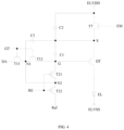
- FIG. 4 is a schematic diagram of a working state of the pixel driving circuit in FIG. 2 during a threshold compensation period
- FIG. 5 is a schematic diagram of a working state of the pixel driving circuit in FIG. 2 during a data writing-in period
- FIG. 6 is a schematic diagram of a working state of the pixel driving circuit in FIG. 2 during a light-emitting period
- FIG. 7 is a first timing sequence diagram of the pixel driving circuit provided by the embodiment of the present disclosure.
- FIG. 8 is a second timing sequence diagram of the pixel driving circuit provided by the embodiment of the present disclosure.
- FIG. 9 is a third timing sequence diagram of the pixel driving circuit provided by the embodiment of the present disclosure.
- FIG. 10 is a schematic diagram of a second structure of a pixel driving circuit provided by an embodiment of the present disclosure.
- FIG. 11 is a second circuit diagram of a pixel driving circuit provided by an embodiment of the present disclosure.
- FIG. 12 is a schematic diagram of a third structure of a pixel driving circuit provided by an embodiment of the present disclosure.
- FIG. 13 is a third circuit diagram of a pixel driving circuit provided by an embodiment of the present disclosure.
- FIG. 14 is a schematic diagram of a fourth structure of a pixel driving circuit provided by an embodiment of the present disclosure.
- FIG. 15 is a fourth circuit diagram of a pixel driving circuit provided by an embodiment of the present disclosure.
- an embodiment of the present disclosure provides a pixel driving circuit for driving a light-emitting element EL, and the pixel driving circuit includes:
- a driving transistor DT i.e., a driving sub-circuit 3
- a second electrode of the driving transistor DT is connected to the light-emitting element EL
- a power control sub-circuit 1 respectively connected to a first control terminal EM, a power signal input terminal ELVDD and a first electrode of the driving transistor DT;
- a data writing sub-circuit 2 respectively connected to a first common node N 1 , a gate line GT in a corresponding row, a data line DA in a corresponding column and a gate electrode of the driving transistor DT, and configured to, under the control of the gate line GT, control to connect or disconnect the data line DA and the first common node N 1 , and control to connect or disconnect the first common node N 1 and the gate electrode of the driving transistor DT;
- a first reset control sub-circuit 51 respectively connected to a second common node N 2 , a reset signal line RE, the gate electrode of the driving transistor DT, and a reference voltage input terminal Ref; configured to, under the control of the reset signal line RE, control to connect or disconnect the reference voltage input terminal Ref and a second common node N 2 , and control to connect or disconnect the second common node N 2 and the gate electrode of the driving transistor DT;
- a first capacitor unit 6 a first end of the first capacitor unit 6 is connected to the gate electrode of the drive transistor DT, and a second end of the first capacitor unit 6 is connected to the first electrode of the drive transistor DT;
- a second capacitor unit 7 a first end of the second capacitor unit 7 is connected to the first electrode of the driving transistor DT, and a second end of the second capacitor unit 7 is connected to the power signal input end ELVDD;
- a third capacitor unit 9 a first end of the third capacitor unit 9 is connected to the first common node N 1 and/or the second common node N 2 , and a second end of the third capacitor unit 9 is connected to the first electrode of the driving transistor DT.
- the pixel driving circuit is applied to a display device, and the display device includes a substrate, a plurality of pixel driving circuits arranged in an array on the substrate, and light-emitting elements EL arranged at a side of the plurality of pixel driving circuits away from the substrate and corresponding to the plurality of pixel driving circuits in a one-to-one manner.
- the light-emitting element EL specifically includes an anode, a light-emitting functional layer, and a cathode that are sequentially stacked along a direction away from the substrate, and the anode of the light-emitting element EL can be connected to the corresponding pixel driving circuit and receive the driving signal provided by the corresponding pixel driving circuit, the cathode can be connected to a negative power supply signal line in the display device, receive a negative power supply signal provided by the negative power supply signal line, and the light-emitting functional layer is used to emit light under the action of the anode and the cathode.
- a reset period P 1 as shown in FIG. 3 , the power signal input terminal ELVDD inputs the power supply voltage Vdd, and under the control of the first control terminal EM, the power control sub-circuit 1 controls to connect the power signal input terminal ELVDD and the first electrode of the driving transistor DT (i.e., the nodes S), so that the potential of the first electrodes of the driving transistor DT becomes Vdd.
- the reference voltage input terminal Ref inputs the reference voltage Vref, under the control of the corresponding reset signal line RE, the first reset control sub-circuit 51 controls to connect the reference voltage input terminal Ref and the second common node N 2 , and controls to connect the second common node N 2 and the gate electrode of the driving transistor DT (i.e., the node G), so that the potential of the second common node N 2 and the potential of the gate electrode of the driving transistor DT both become Vref, so that the voltages of the gate electrode and the first electrode of the driving transistor DT are both in a fixed bias state, and the driving transistor DT is turned on to prepare for a threshold compensation period P 2 .
- both the potential of the second common node N 2 and the potential of the gate electrode of the driving transistor DT can be changed to Vref, and the potential of the first electrode of the driving transistor DT can be changed to Vdd, thereby initializing the driving transistor DT.
- Vref-Vdd should be less than the threshold voltage Vth of the driving transistor DT.
- the light-emitting element EL can be an OLED
- the anode of the light-emitting element EL is the anode of the OLED
- the cathode of the light-emitting element EL is the cathode of the OLED
- the cathode of the light-emitting element EL is connected to the low-level signal input terminal ELVSS
- the low-level signal input terminal ELVSS can be connected to a negative power supply signal line for inputting a low-level signal.
- the reference voltage input terminal Ref inputs the reference voltage Vref
- the first reset control sub-circuit 51 continues to control to connect the reference voltage input terminal Ref and the second common node N 2 and control to connect the second common node N 2 and the gate electrode of the driving transistor DT, so that the potential of the second common node N 2 and the potential of the gate electrode of the driving transistor DT are kept at Vref.
- the power control sub-circuit 1 controls to disconnect the power signal input terminal ELVDD from the first electrode of the driving transistor DT, so that the first electrode of the driving transistor DT is in a floating state, a discharge process is implemented on the driving transistor DT, and the driving transistor DT changes from the on state to the off state, so that the potential of the first electrode of the driving transistor DT changes from Vdd to Vref-Vth, and Vth is the threshold voltage of the driving transistor DT.
- the potential of the first electrode of the driving transistor DT starts to decrease from Vdd until it drops to Vref-Vth, a conduction condition of the driving transistor DT is not satisfied, so that the driving transistor DT is turned off.
- the first reset control sub-circuit 51 controls to disconnect the reference voltage input terminal Ref from the second common node N 2 , and control to disconnect the second common node N 2 from the gate electrode of the driving transistor DT.
- the power control sub-circuit 1 continues to control to disconnect the power signal input terminal ELVDD from the first electrode of the driving transistor DT.
- the data line DA of the corresponding column inputs the data voltage Vdata, and under the control of the gate line GT of the corresponding row, the data writing-in sub-circuit 2 controls to connect the data line DA of the corresponding column and the first common node N 1 , and controls to connect the first common node N 1 and the gate electrode of the driving transistor DT, so that the potential of the gate electrode of the driving transistor DT, the potential of the first common node N 1 and the potential of the second common node N 2 changes from Vref to Vdata.
- the potential of the first electrode of the driving transistor DT changes from Vref-Vth to [(C1+C3)/(C1+C2+C3)](Vdata-Vref)+Vref ⁇ Vth.
- the potential of the gate electrode of the driving transistor DT changes from Vref to Vdata
- the amount of change in the potential of the gate electrode of the driving transistor DT is Vdata-Vref.
- the potential of the first electrode of the driving transistor DT becomes [C1+C3/(C1+C2+C3)](Vdata-Vref)+Vref ⁇ Vth.
- C1 represents the capacitance value of the first capacitor included in the first capacitor unit 6
- C2 represents the capacitance value of the second capacitor included in the second capacitor unit 7
- C3 represents the capacitance value of the third capacitor included in the third capacitor unit 9 .
- the first reset control sub-circuit 51 continues to control to disconnect the reference voltage input terminal Ref from the second common node N 2 and control to disconnect the second common node N 2 from the gate electrode of the driving transistor DT.
- the power supply signal input terminal ELVDD inputs a power supply voltage Vdd, and under the control of the first control terminal EM, the power supply control sub-circuit 1 controls to connect the power supply signal input terminal ELVDD and the first electrode of the first driving transistor DT, so that the potential of the first electrode of the driving transistor DT change from [C1+C3/(C1+C2+C3)](Vdata-Vref)+Vref ⁇ Vth to Vdd.
- the data writing-in sub-circuit 2 controls to disconnect the data line DA from the first common node N 1 , and controls to disconnect the first common node N 1 from the gate electrode of the driving transistor DT, under the coupling control of the first capacitor unit 6 , the second capacitor unit 7 and the third capacitor unit 9 , the potential of the gate electrode of the driving transistor DT, the potential of the first common node N 1 and the potential of the second common node N 2 are all changed from Vdata to [C2/(C1+C2+C3)](Vdata-Vref)+Vth+Vdd, so that the driving transistor DT is turned on to drive the light-emitting element EL to emit light.
- the potential of the first electrode of the driving transistor DT changes from [(C1+C3)/(C1+C2+C3)](Vdata-Vref)+Vref ⁇ Vth to Vdd
- the amount of the change of the potential of the first electrode of the driving transistor DT is Vdd ⁇ [(C1+C3)/(C1+C2+C3)](Vdata-Vref) ⁇ Vref+Vth
- the potential of the gate electrode of the driving transistor DT, the potential of the first common node N 1 , and the potential of the second common node N 2 all become Vdata+Vdd ⁇ [(C1+C3)/(C1+C2+C3)](Vdata-Vref) ⁇ Vref+Vth, that is [C2/(C1+C2+C3)](Vdata-Vref)+Vth+Vdd.
- Table 1 For a more intuitive description of the potentials of the first common node N 1 , the second common node N 2 , the gate electrode of the driving transistor DT, and the first electrode of the driving transistor DT in different time periods, Table 1 is referred as below.
- Table 1 corresponds to the case where the first end of the third capacitor unit 9 is connected to both the first common node N 1 and the second common node N 2 .
- the driving transistor DT in the reset period P 1 , the potential of the gate electrode of the driving transistor DT is changed to Vref, and the potential of the first electrode of the driving transistor DT is changed to Vdd, so that the voltages of the gate electrode and the first electrode of the driving transistor DT are both in a fixed bias state, the driving transistor DT is initialized. No matter each display unit displays a black picture or a white picture in a previous frame, the driving transistor DT starts the display of the next frame from a fixed bias state, which greatly improves the short-term afterimage problem caused by the hysteresis effect.
- the threshold compensation period P 2 by controlling the first electrode of the driving transistor DT to be disconnected from the power supply signal input terminal ELVDD, a discharge process is implemented on the driving transistor DT until the driving transistor DT is turned off, so that the potential of the first electrode of the driving transistor DT is changed from Vdd to Vref-Vth.
- the data voltage Vdata is written during the data writing-in period P 3 , so that the potential of the gate electrode of the driving transistor DT, the potential of the first common node N 1 and the potential of the second common node N 2 are all changed from Vref to Vdata.
- the potential of the first electrode of the driving transistor DT changes from Vref-Vth to [(C1+C3)/(C1+C2+C3)](Vdata-Vref)+Vref ⁇ Vth
- the potential of the first electrode of the driving transistor DT becomes the power supply voltage Vdd, so that the potential of the gate electrode of the driving transistor DT, the potential of the first common node N 1 and the potential of the second common node N 2 are all changed from Vdata to [C2/(C1+C2+C3)](Vdata-Vref)+Vth+Vdd, so that the driving transistor DT is turned on
- k is a constant.
- the driving current I is only related to the data voltage Vdata and the reference voltage Vref, but is not related to the threshold voltage Vth of the driving transistor DT and the power supply voltage Vdd; therefore, in the pixel driving circuit provided by the embodiment of the present disclosure, the uniformity of the driving current is improved, and the influence of the IR Drop generated on the power signal line connected to the power signal input terminal ELVDD and the threshold voltage of the driving transistor DT on the display brightness uniformity of the large-size display device is solved, the display brightness uniformity of the display device is ensured.
- the pixel driving circuit provided by the embodiment of the present disclosure, by connecting the first end of the third capacitor unit 9 to the first common node N 1 and/or the second common node N 2 , connecting the second end of the third capacitor unit 9 to the first electrode of the driving transistor DT, so that during the light-emitting period P 4 , the potential of the gate electrode of the driving transistor DT is the same as the potential of the first common node N 1 , and/or, the potential of the gate electrode of the driving transistor DT is the same as the potential of the second common node N 2 , and at the same time, the potentials of the first common node N 1 and the second common node N 2 can be maintained through the third capacitor unit 9 ; therefore, the pixel driving circuit provided by the embodiment of the present disclosure effectively reduces the leakage current of the gate electrode of the driving transistor DT through the data writing sub-circuit 2 and the first reset control sub-circuit 51 , even if in the case of low-frequency driving, the potential of the gate electrode of the driving transistor
- the data writing-in sub-circuit 2 includes a first double-gate transistor, and the first double-gate transistor includes a first sub-transistor T 11 and a second sub-transistor T 12 ; the gate electrode of the first sub-transistor T 11 is connected to the gate electrode of the second sub-transistor T 12 , and is connected to the gate line GT of corresponding row, and the first electrode of the first sub-transistor T 11 is connected to the data line DA of corresponding column, the second electrode of the first sub-transistor T 11 is connected to the first common node N 1 ; the first electrode of the second sub-transistor T 12 is connected to the first common node N 1 , and the second electrode of the second sub-transistor T 12 is connected to the gate electrode of the driving transistor DT.
- the specific structure of the data writing-in sub-circuit 2 is various.
- the data writing-in sub-circuit 2 includes a first double-gate transistor, and the first double-gate transistor includes a first sub-transistor T 11 and the second sub-transistor T 12 ; the gate electrode of the first sub-transistor T 11 and the gate electrode of the second sub-transistor T 12 form an integral structure; the second electrode of the first sub-transistor T 11 and the first electrode of the second sub-transistor T 12 forms an integral structure; the first common node N 1 is located between the second electrode of the first sub-transistor T 11 and the first electrode of the second sub-transistor T 12 .
- the threshold compensation period P 2 and the light-emitting period P 4 under the control of the scan signal transmitted by the gate line GT of corresponding row, the first sub-transistor T 11 and the second sub-transistors T 12 are all turned off.
- the first sub-transistor T 11 and the second sub-transistor T 12 are both turned on.
- the data writing-in sub-circuit 2 includes the first double-gate transistor, so that the data writing-in sub-circuit 2 has a simple structure and occupies a smaller layout space during actual layout, which is beneficial to improve the resolution of the display device.
- the data writing-in sub-circuit 2 can also include two independent transistor structures, and the two independent transistor structures are arranged according to the connection mode of the first sub-transistor T 11 and the second sub-transistor T 12 .
- the first reset control sub-circuit 51 includes a second dual-gate transistor, and the second dual-gate transistor includes a third sub-transistor T 22 and a fourth sub-transistor T 21 ; the gate electrode of the third sub-transistor T 22 is connected to the gate electrode of the fourth sub-transistor T 21 , and is connected to the reset signal line RE, and the first electrode of the third sub-transistor T 22 is connected to the reference voltage input terminal Ref, the second electrode of the third sub-transistor T 22 is connected to the second common node N 2 ; the first electrode of the fourth sub-transistor T 21 is connected to the second common node N 2 , and the second electrode of the fourth sub-transistor T 21 is connected to the gate electrode of the driving transistor DT.
- the specific structure of the first reset control sub-circuit 51 is various.
- the first reset control sub-circuit 51 includes a second double-gate transistor, and the second double-gate transistor includes a third sub-transistor T 22 and the fourth sub-transistor T 21 ; the gate electrode of the third sub-transistor T 22 and the gate electrode of the fourth sub-transistor T 21 form an integral structure; the second electrode of the third sub-transistor T 22 and the first electrodes of the fourth sub-transistor T 21 form an integral structure; the second common node N 2 is located between the second electrodes of the third sub-transistors T 22 and the first electrodes of the fourth sub-transistors T 21 .
- the third sub-transistor T 22 and the fourth sub-transistor T 21 are both turned on.
- the third sub-transistor T 22 and the fourth sub-transistor T 21 are both turned off.
- the first reset control sub-circuit 51 includes the second double-gate transistor, so that the first reset control sub-circuit 51 has a simple structure and occupies a smaller layout space during actual layout, which is beneficial to improve the resolution of the display device.
- the first reset control sub-circuit 51 can also include two independent transistor structures, and the two independent transistor structures are connected according to the connection mode of the third sub-transistor T 22 and the fourth sub-transistor T 21 .
- the pixel driving circuit further includes a second reset control sub-circuit 52 , and the second reset control sub-circuit 52 is respectively connected to the reset signal line RE, the second electrode of the driving transistor DT, and the reference voltage input terminal Ref; is configured to connect or disconnect the reference voltage input terminal Ref and the second electrode of the driving transistor DT under the control of the reset signal line RE.
- the second reset control sub-circuit 52 controls to connect the reference voltage input terminal Ref and the second electrode of the driving transistor DT.
- the second reset control sub-circuit 52 controls to disconnect the reference voltage input terminal Ref from the second electrode of the driving transistor DT.
- the second reset control sub-circuit 52 can reset the anode of the light-emitting element EL during the reset period P 1 and the threshold compensation period P 2 .
- the second reset control sub-circuit 52 includes a fifth transistor T 5 , the gate electrode of the fifth transistor T 5 is connected to the reset signal line RE, the first electrode of the fifth transistor T 5 is connected to the reference voltage input terminal Ref, and the second electrode of the fifth transistor T 5 is connected to the second electrode of the driving transistor DT.
- the specific structure of the second reset control sub-circuit 52 is various.
- the second reset control sub-circuit 52 includes the fifth transistor T 5 .
- the fifth transistor T 5 is turned on, thereby controlling the connection between the reference voltage input terminal Ref and the second electrode of the driving transistor DT.
- the fifth transistor T 5 is turned off, thereby controlling the disconnection of the reference voltage input terminal Ref from the second electrode of the driving transistor DT.
- the pixel driving circuit further includes a third reset control sub-circuit 53 , and the third reset control sub-circuit 53 is respectively connected to the reset signal line RE, the second electrode of the driving transistor DT is connected to the initialization voltage input terminal Iint; is configured to control to connect or disconnect the initialization voltage input terminal Iint and the second electrode of the driving transistor DT under the control of the reset signal line RE.
- the third reset control sub-circuit controls to connect the initialization voltage input terminal Iint and the second electrode of the drive transistor DT.
- the third reset control sub-circuit controls to disconnect the initialization voltage input terminal lint from the second electrode of the driving transistor DT.
- the second reset control sub-circuit 52 can reset the anode of the light-emitting element EL during the reset period P 1 and the threshold compensation period P 2 .
- the third reset control sub-circuit 53 is connected to the reset signal line RE, the second electrode of the driving transistor DT, and the initialization voltage input terminal Iint respectively, so that the initialization signal outputted by the initialization voltage input terminal Iint and the reference voltage signal outputted by the reference voltage input terminal Ref can be independently controlled, so that the potential of the reference voltage signal is not limited, and the pixel driving circuit has a wider application.
- the third reset control sub-circuit 53 includes a fifth transistor T 5 , the gate electrode of the fifth transistor T 5 is connected to the reset signal line RE, the first electrode of the fifth transistor T 5 is connected to the initialization voltage input terminal Iint, and the second electrode of the fifth transistor T 5 is connected to the second electrode of the driving transistor DT.
- the fifth transistor T 5 is turned on, so that the initialization voltage input terminal Iint and the second electrode of the driving transistor DT are controlled to be connected.
- the fifth transistor T 5 is turned off, and the initialization voltage input terminal Iint is controlled to be disconnected from the second electrode of the driving transistor DT.
- the pixel driving circuit further includes a light-emitting control sub-circuit 8 , and the second electrode of the driving transistor DT is connected to the light-emitting element EL through the light-emitting control sub-circuit 8 ; the light-emitting control sub-circuit 8 is respectively connected to the first control terminal EM, the second electrode of the driving transistor DT and the light-emitting element EL, and is configured to connect or disconnect the second electrode of the driving transistor DT and the light emitting element EL under the control of the first control terminal EM.
- the light-emitting control sub-circuit 8 controls to connect the second electrode of the driving transistor DT and the anode of the light-emitting element EL.
- the light-emitting control sub-circuit 8 controls to disconnect the second electrode of the driving transistor DT from the anode of the light-emitting element EL, so that abnormal light emitting of the light emitting element EL during the threshold value compensation period P 2 and the data writing-in period P 3 is avoided.
- the light-emitting control sub-circuit 8 includes a sixth transistor T 6 , the gate electrode of the sixth transistor T 6 is connected to the first control terminal EM, and the first electrode of the sixth transistor T 6 is connected to the second electrode of the driving transistor DT, and the second electrode of the sixth transistor T 6 is connected to the light emitting element EL.
- the specific structure of the light-emitting control sub-circuit 8 is various.
- the light-emitting control sub-circuit 8 includes the sixth transistor T 6 .
- the sixth transistor T 6 is turned on to control to connect the second electrode of the driving transistor DT and the anode of the light-emitting element EL.
- the sixth transistor T 6 is turned off, and controls to disconnect the second electrode of the driving transistor DT from the anode of the light-emitting element EL, so that abnormal light emitting of the light-emitting element EL during the threshold compensation period P 2 and the data writing-in period P 3 is avoided.
- the power control sub-circuit 1 includes a seventh transistor T 7 , the gate electrode of the seventh transistor T 7 is connected to the first control terminal EM, and the first electrode of the seventh transistor T 7 is connected to the power signal line input terminal, and the second electrode of the seventh transistor T 7 is connected to the first electrode of the driving transistor DT.
- the specific structure of the power supply control sub-circuit 1 is various.
- the power supply control sub-circuit 1 includes the seventh transistor T 7 .
- the seventh transistor T 7 is turned on, and controls to connect the power signal line input terminal and the first electrode of the driving transistor DT.
- the seventh transistor T 7 is turned off, and controls to disconnect the power signal line input terminal from the first electrode of the driving transistor DT.
- Embodiments of the present disclosure further provide a display device, including the pixel driving circuit provided by the above embodiments.
- the driving transistor DT starts to display the next frame from the fixed bias state, which greatly improves the short-term afterimage problem caused by the hysteresis effect.
- the uniformity of the driving current is improved, and the influence of the IR Drop generated on the power signal line connected to the power signal input terminal ELVDD and the threshold voltage of the driving transistor DT on the display brightness uniformity of the large-size display device is solved, the display brightness uniformity of the display device is ensured.
- the pixel driving circuit provided by the above embodiment effectively reduces the current leakage of the gate electrode of the driving transistor DT through the data writing-in sub-circuit 2 and the first reset control sub-circuit 51 , even in the case of low-frequency driving, the potential of the gate electrode of the driving transistor DT can also be maintained, so that the flicker problem of the display device during display is improved.
- the display device provided by the embodiment of the present disclosure also has the above beneficial effects when including the pixel driving circuit provided by the above embodiment, and which is not repeated.
- the display device may be any product or component with a display function, such as a TV, a monitor, a digital photo frame, a mobile phone, and a tablet computer.
- the display device further includes a gate driving circuit, a reset signal control circuit, a plurality of gate lines GT and a plurality of reset signal lines RE;
- the gate driving circuit includes a plurality of first shift register units corresponding to the plurality of gate lines GT in a one-to-one manner, and each first shift register unit is connected to a corresponding gate line GT, and is configured to provide a scan signal for the corresponding gate line GT.
- the reset signal control circuit includes a plurality of second shift register units corresponding to the plurality of reset signal lines RE in a one-to-one manner, and each second shift register unit is connected to the corresponding reset signal line RE, and is configured to provide a reset signal to the reset signal line RE.
- the display device includes a plurality of gate lines GT and a plurality of data lines DA, and the gate lines GT and the data lines DA are crossing to each other.
- the display device further includes a plurality of reset signal lines RE and a plurality of first control signal lines, and the extension direction of the reset signal lines RE and the first control signal lines are substantially the same as the extension direction of the gate lines GT.
- the gate lines GT, the reset signal lines RE and the first control signal lines all extend along a first direction
- the data lines DA extends along a second direction.
- the display device includes a plurality of pixel driving circuits arranged in an array, and the plurality of pixel driving circuits can be divided into a plurality of rows of pixel driving circuits and a plurality of columns of pixel driving circuits.
- the plurality of rows of pixel driving circuits are arranged in sequence along the second direction, and each row of pixel driving circuits includes a plurality of pixel driving circuits arranged in sequence along the first direction.
- the plurality of columns of pixel driving circuits are arranged in sequence along the first direction, and each column of pixel driving circuits includes a plurality of pixel driving circuits arranged in sequence along the second direction.
- the plurality of rows of pixel driving circuits correspond to the plurality of gate lines GT in a one-to-one manner, and the gate lines GT are respectively connected to data writing-in sub-circuits 2 included in pixel driving circuits in a row of pixel driving circuits.
- the plurality of rows of pixel driving circuits correspond to the plurality of reset signal lines RE in a one-to-one manner, and the reset signal line RE is connected to the first reset control sub-circuit 51 included in each pixel driving circuit in a corresponding row of pixel driving circuits.
- the plurality of rows of pixel driving circuits correspond to the plurality of first control signal lines in a one-to-one manner, and the first control signal line is connected to the first control terminals EM connected to each pixel driving circuit in a corresponding row of pixel driving circuits.
- the display device further includes a gate driving circuit and a reset signal control circuit arranged in a peripheral area of the display device, and the gate driving circuit includes a plurality of first shift register units corresponding to the plurality of gate lines GT in a one-to-one manner, the first shift register unit is connected to the corresponding gate line GT, and is used to provide a scanning signal for the corresponding gate line GT;
- the reset signal control circuit includes a plurality of second shift register units corresponding to the plurality of reset signal lines RE in a one-to-one manenr, the second shift register unit is connected to the corresponding reset signal line RE, and is used for providing a reset signal to the corresponding reset signal line RE.
- 1H marked in FIG. 7 , FIG. 8 and FIG. 9 represents one row period.
- the threshold compensation and data writing-in are two independent processes, that is, the threshold compensation process is performed in the threshold compensation period P 2 , and the data writing-in process is performed in the data writing-in period P 3 .
- the display device include the gate driving circuit and the reset signal control circuit, so that the signal transmitted on the gate line GT and the signal transmitted on the reset signal line RE are independently controlled, when the display device is refreshed at a high frame rate, although the data voltage writing time will be reduced, the reset signal control circuit controls the effective level time of the signal transmitted on the reset signal line RE to be extended, so as to ensure that the pixel driving circuit has a longer compensation in one working cycle time and ensure the compensation effect on the pixel drive circuit.
- An embodiment of the present disclosure further provides a method for driving a pixel driving circuit, which is applied to the pixel driving circuit provided in the above-mentioned embodiments, and the method includes: in each working cycle,
- the power supply signal input terminal ELVDD inputs the power supply voltage Vdd
- the power supply control sub-circuit 1 controls to connect the power supply signal input terminal ELVDD and the first electrode of the driving transistor DT.
- the reference voltage input terminal Ref inputs the reference voltage Vref
- the first reset control sub-circuit 51 controls to connect the reference voltage input terminal Ref and the second common node N 2 , and controls to connect the second common node N 2 and the gate electrode of the driving transistor DT, so that the driving transistor DT is in an on state;
- the power control sub-circuit 1 controls to disconnect the power signal input terminal ELVDD from the first electrode of the driving transistor DT, so that the driving transistor DT is changed from an on state to an off state, the potential of the first electrode of the driving transistor DT changes from Vdd to Vref-Vth, where Vth is the threshold voltage of the driving transistor DT;
- the first reset control sub-circuit 51 controls to disconnect the reference voltage input terminal Ref from the second common node N 2 , and control to disconnect the second common node N 2 from the gate electrode of the driving transistor DT;
- the data line DA of corresponding column inputs the data voltage Vdata, and under the control of the gate line GT of corresponding row, the data writing-in sub-circuit 2 controls to connect the data line DA and the first common node N 1 , and control to connect the first common node N 1 and the gate electrode of the driving transistor DT, so that the potential of the gate electrode of the driving transistor DT, the potential of the first common node N 1 and the potential of the second common node N 2 are all changed from Vref to Vdata, and the potential of the first electrode of the driving transistor DT is changed under the coupling action of a first capacitor unit 6 , a second capacitor unit 7 and a third capacitor unit 9 ;
- the power signal input terminal ELVDD inputs the power supply voltage Vdd
- the power control sub-circuit 1 controls to connect the power signal input terminal ELVDD and the first electrode of the driving transistors DT, under the control of the gate line GT of corresponding row
- the data writing-in sub-circuit 2 controls to disconnect the data line DA from the first common node N 1 , and control to disconnect the first common node N 1 from the gate electrode of the driving transistor DT, the potential of the gate electrode of the driving transistor DT, the potential of the first common node N 1 and the potential of the second common node N 2 are changed under the coupling control of the first capacitor unit 6 , the second capacitor unit 7 and the third capacitor unit 9 , so that the driving transistor DT is turned on to drive light-emitting element EL to emit light.
- the driving transistor DT starts the display of the next frame from the fixed bias state, which greatly improves the short-term afterimage problem caused by the hysteresis effect.
- the threshold compensation period P 2 by controlling the first electrode of the driving transistor DT to be disconnected from the power supply signal input terminal ELVDD, a discharge process is implemented on the driving transistor DT until the driving transistor DT is turned off, so that the potential of the first electrode of the driving transistor DT is Changed from Vdd to Vref-Vth.
- the data voltage Vdata is written during the data writing-in period P 3 , so that the potential of the gate electrode of the driving transistor DT, the potential of the first common node N 1 and the potential of the second common node N 2 are all changed from Vref to Vdata.
- the potential of the first electrode of the driving transistor DT changes from Vref-Vth to [(C1+C3)/(C1+C2+C3)](Vdata-Vref)+Vref ⁇ Vth
- the potential of the first electrode of the driving transistor DT becomes the power supply voltage Vdd, so that the potential of the gate electrode of the driving transistor DT, the potential of the first common node N 1 and the potential of the second common node N 2 are changed from Vdata to [C2/(C1+C2+C3)](Vdata-Vref)+Vth+Vdd
- k is a constant.
- the driving current I is only related to the data voltage Vdata and the reference voltage Vref, but is not related to the threshold voltage Vth of the driving transistor DT and the power supply voltage Vdd; therefore, the driving method provided by the embodiment of the present disclosure is used to drive the pixel driving circuit, the uniformity of the driving current is improved, and the influence of the IR Drop generated on the power signal line connected to the power signal input terminal ELVDD and the threshold voltage of the driving transistor DT on the display brightness uniformity of the large-size display device is solved, the display brightness uniformity of the display device is ensured.
- the first end of the third capacitor unit 9 is connected to the first common node N 1 and/or the second common node N 2
- the second end of the third capacitor unit 9 is connected to the first electrode of the driving transistor DT, so that during the light-emitting period P 4 , the potential of the gate electrode of the driving transistor DT is the same as the potential of the first common node N 1 and/or, the potential of the gate electrode of the driving transistor DT is the same as the potential of the second common node N 2 , the potentials of the first common node N 1 and the second common node N 2 can both be maintained through the third capacitor unit 9 .
- the leakage current of the gate electrode of the driving transistor DT flowing through the data writing-in sub-circuit 2 and the first reset control sub-circuit 51 is effectively reduced, even in the case of low-frequency driving, the potential of the gate electrode of the driving transistor DT may be maintained, thereby greatly improving the flickering of the display device during display.
- the display device to which the pixel driving circuit is applied further includes a gate driving circuit, a reset signal control circuit, a plurality of gate lines GT and a plurality of reset signal lines RE;
- the gate driving circuit includes a plurality of first shift register units corresponding to the plurality of gate lines GT in a one-to-one manner, and each first shift register unit is connected to the corresponding gate line GT, and is used to provide a scan signal for the corresponding gate line GT;
- the reset signal control circuit includes a plurality of second shift register units corresponding to the plurality of reset signal lines RE in a one-to-one manner, and each second shift register unit is connected to the corresponding reset signal line RE, and is used to provide a reset signal for the corresponding reset signal line RE;
- the first reset control sub-circuit 51 controls to connect the reference voltage input terminal Ref and the second common node N 2 , and controls to connect the second common node N 2 and the gate electrode of the driving transistors DT for a first time length b; during the data writing-in period P 3 , the data writing-in sub-circuit 2 controls to connect the data line DA and the first common node N 1 and controls to connect the first common node N 1 and the gate electrode of the driving transistor DT for a second time length c; the first time length b is greater than the second time length c.
- FIG. 8 shows a schematic diagram of the working timing sequence of the pixel driving circuit when the display device is refreshed at a high frame rate.
- the first reset control sub-circuit 51 controls to connect the reference voltage input terminal Ref and the second common node N 2 , and controls to connect the second common node N 2 and the gate electrode of the driving transistor DT for a third time length a.
- the first reset control sub-circuit 51 controls to connect the reference voltage input terminal Ref and the second common node N 2 , and controls to connect the second common node N 2 and the gate electrode of the driving transistor DT for a first time length b.
- the data writing sub-circuit 2 controls to connect the data line DA and the first common node N 1 , and controls to connect the first common node N 1 and the gate electrode of the driving transistor DT for a second time length c.
- the display device includes the gate driving circuit and the reset signal control circuit, the signal transmitted on the gate line GT and the signal transmitted on the reset signal line RE can be independently controlled, so that the display device has a high refresh frame rate, although the data voltage writing-in time (i.e. the second time length c) will be shortened, the reset signal control circuit may control the effective level time (i.e. the first time) of the signal transmitted on the reset signal line RE to be extended, so that the first time length b is greater than the second time length c, thereby ensuring that the pixel driving circuit has a longer compensation time in one working cycle and ensuring the compensation effect on the pixel driving circuit.
- the effective level time i.e. the first time
- the pixel driving circuit may further include a light-emitting control sub-circuit 8 , and the second electrode of the driving transistor DT is connected to the light-emitting element EL through the light-emitting control sub-circuit 8 ; the light-emitting control sub-circuit 8 is respectively connected to the first control terminal EM, the second electrode of the driving transistor DT and the light-emitting element EL; the driving method further includes:
- the light-emitting control sub-circuit 8 controls to disconnect the second electrode of the driving transistor DT from the light-emitting elements EL, so that the light-emitting elements EL do not emit light during the threshold compensation period P 2 and the data writing-in period P 3 .
- the light-emitting control sub-circuit 8 controls to connect the second electrode of the driving transistor DT and the anode of the light-emitting element EL.
- the light-emitting control sub-circuit 8 controls to disconnect the second electrode of the driving transistor DT from the anode of the light-emitting element EL, so as to avoid abnormal light emission of the light emitting element EL druing the threshold value compensation period P 2 and the data writing-in period P 3 .
Landscapes
- Engineering & Computer Science (AREA)
- Physics & Mathematics (AREA)
- Computer Hardware Design (AREA)
- General Physics & Mathematics (AREA)
- Theoretical Computer Science (AREA)
- Control Of Indicators Other Than Cathode Ray Tubes (AREA)
- Control Of El Displays (AREA)
Abstract
Description
| TABLE 1 | ||||||
| P1 | P2 | P3 | P4 | |||
| S | Vdd | Vref − | [(C1 + C3)/ | Vdd | ||
| Vth | (C1 + C2 + | |||||
| C3)](Vdata − | ||||||
| Vref) + | ||||||
| Vref − Vth | ||||||
| G | Vref | Vref | Vdata | [C2/(C1 + C2 + | ||
| C3)](Vdata − Vref) + | ||||||
| Vth + Vdd | ||||||
| N1 | Vref | Vref | Vdata | [C2/(C1 + C2 + | ||
| C3)](Vdata − Vref) + | ||||||
| Vth + Vdd | ||||||
| N2 | Vref | Vref | Vdata | [C2/(C1 + C2 + | ||
| C3)](Vdata − Vref) + | ||||||
| Vth + Vdd | ||||||
Vgs=[C2/(C1+C2+C3)](Vdata-Vref)+Vth Formula (1)
I=k(Vgs-Vth)2 Formula (2)
I=k{[C2/(C1+C2+C3)](Vdata-Vref)}2 Formula (3)
Vgs=[C2/(C1+C2+C3)](Vdata-Vref)+Vth Formula(1)
I=k(Vgs-Vth)2 Formula (2)
I=k{[C2/(C1+C2+C3)](Vdata-Vref)}2 Formula (3)
Claims (15)
Applications Claiming Priority (3)
| Application Number | Priority Date | Filing Date | Title |
|---|---|---|---|
| CN202010430333.3 | 2020-05-20 | ||
| CN202010430333.3A CN111477179B (en) | 2020-05-20 | 2020-05-20 | A pixel driving circuit, a driving method thereof, and a display device |
| PCT/CN2021/087383 WO2021233027A1 (en) | 2020-05-20 | 2021-04-15 | Pixel drive circuit and driving method therefor, and display device |
Publications (2)
| Publication Number | Publication Date |
|---|---|
| US20220375408A1 US20220375408A1 (en) | 2022-11-24 |
| US11735113B2 true US11735113B2 (en) | 2023-08-22 |
Family
ID=71762782
Family Applications (1)
| Application Number | Title | Priority Date | Filing Date |
|---|---|---|---|
| US17/639,245 Active US11735113B2 (en) | 2020-05-20 | 2021-04-15 | Pixel driving circuit, method of driving the same and display device |
Country Status (3)
| Country | Link |
|---|---|
| US (1) | US11735113B2 (en) |
| CN (1) | CN111477179B (en) |
| WO (1) | WO2021233027A1 (en) |
Cited By (3)
| Publication number | Priority date | Publication date | Assignee | Title |
|---|---|---|---|---|
| US20240194138A1 (en) * | 2022-12-12 | 2024-06-13 | Lg Display Co., Ltd. | Display panel and display device including the same |
| US12106717B2 (en) * | 2021-10-21 | 2024-10-01 | Samsung Display Co., Ltd. | Pixel and display device including pixel |
| US20250182687A1 (en) * | 2023-12-05 | 2025-06-05 | Samsung Display Co., Ltd. | Pixel and display device including the same |
Families Citing this family (32)
| Publication number | Priority date | Publication date | Assignee | Title |
|---|---|---|---|---|
| CN111445856B (en) * | 2020-05-13 | 2021-04-09 | 京东方科技集团股份有限公司 | Driving circuit, driving method, display panel and display device |
| CN111477179B (en) * | 2020-05-20 | 2021-10-22 | 京东方科技集团股份有限公司 | A pixel driving circuit, a driving method thereof, and a display device |
| CN111933080A (en) * | 2020-08-20 | 2020-11-13 | 京东方科技集团股份有限公司 | Pixel circuit, pixel driving method and display device |
| US11605348B2 (en) * | 2020-09-28 | 2023-03-14 | Boe Technology Group Co., Ltd. | Pixel circuit and control method therefor, display device |
| CN117975878A (en) * | 2020-10-20 | 2024-05-03 | 厦门天马微电子有限公司 | Display panel, driving method and display device |
| CN117711325A (en) | 2020-11-27 | 2024-03-15 | 京东方科技集团股份有限公司 | Pixel circuit, display substrate and display device |
| US12236886B2 (en) | 2020-11-27 | 2025-02-25 | Chengdu Boe Optoelectronics Technology Co., Ltd. | Pixel circuit and driving method thereof, display substrate and display device |
| US11915645B2 (en) | 2020-12-25 | 2024-02-27 | Chongqing Boe Display Technology Co., Ltd. | Display panel including extension portion, pixel circuit including voltage stabilizing sub-circuits and display apparatus |
| CN113112955B (en) * | 2021-04-14 | 2022-08-23 | 京东方科技集团股份有限公司 | Pixel circuit, driving method thereof, display substrate and display device |
| CN115529838A (en) | 2021-04-27 | 2022-12-27 | 京东方科技集团股份有限公司 | Drive circuit, drive method, shift register and display device |
| CN115148153B (en) * | 2021-05-17 | 2024-07-26 | 上海天马微电子有限公司 | Display panel and display device |
| CN115836392A (en) | 2021-06-18 | 2023-03-21 | 京东方科技集团股份有限公司 | Display substrate and display device |
| CN115101011B (en) * | 2021-07-21 | 2024-12-13 | 武汉天马微电子有限公司 | Pixel circuit configured to control a light emitting element |
| KR102854058B1 (en) * | 2021-08-24 | 2025-09-04 | 삼성디스플레이 주식회사 | Pixel, display device, and method of operating display device |
| CN114023253B (en) | 2021-11-16 | 2022-09-27 | 武汉华星光电半导体显示技术有限公司 | Pixel circuit and display device |
| CN114078440B (en) * | 2021-11-24 | 2023-06-27 | 京东方科技集团股份有限公司 | Gate drive circuit, display substrate and display device |
| CN114120907A (en) * | 2021-12-02 | 2022-03-01 | 合肥维信诺科技有限公司 | Pixel circuit, display device and driving method thereof |
| CN114582283B (en) * | 2022-03-30 | 2024-05-03 | 云谷(固安)科技有限公司 | Pixel circuit and display panel |
| US12307977B2 (en) * | 2022-04-28 | 2025-05-20 | Sharp Display Technology Corporation | Pixel circuit, display device, and method of driving display device |
| CN114974086B (en) * | 2022-05-19 | 2023-09-26 | 京东方科技集团股份有限公司 | Pixel circuits, display panels and display devices |
| WO2023230790A1 (en) * | 2022-05-30 | 2023-12-07 | 京东方科技集团股份有限公司 | Pixel circuit and driving method therefor, and display device |
| CN114913802B (en) * | 2022-05-31 | 2024-06-21 | Tcl华星光电技术有限公司 | Pixel driving circuit and display panel |
| CN115440167B (en) * | 2022-08-30 | 2023-11-07 | 惠科股份有限公司 | Pixel circuit, display panel and display device |
| JP2025535231A (en) * | 2022-10-11 | 2025-10-24 | 三星ディスプレイ株式會社 | display device |
| US11842677B1 (en) | 2022-12-01 | 2023-12-12 | Novatek Microelectronics Corp. | Pixel circuit of display panel |
| CN118840952B (en) * | 2023-04-25 | 2026-01-06 | 京东方科技集团股份有限公司 | Pixel circuits and their driving methods, display panels, display devices |
| CN116844484A (en) * | 2023-07-24 | 2023-10-03 | 武汉天马微电子有限公司 | Display panel, driving method and display device thereof |
| KR20250024659A (en) * | 2023-08-11 | 2025-02-19 | 삼성디스플레이 주식회사 | Pixel and display device including the same |
| KR20250064214A (en) * | 2023-11-02 | 2025-05-09 | 엘지디스플레이 주식회사 | Pixel circuit and display device including the same |
| CN121171162A (en) * | 2024-06-19 | 2025-12-19 | 合肥京东方卓印科技有限公司 | Pixel circuit and display device |
| CN121214852A (en) * | 2024-06-25 | 2025-12-26 | 京东方科技集团股份有限公司 | Pixel driving circuit, driving method thereof and display device |
| CN118942393B (en) * | 2024-08-30 | 2025-09-19 | 惠科股份有限公司 | Display driving circuit and display panel |
Citations (28)
| Publication number | Priority date | Publication date | Assignee | Title |
|---|---|---|---|---|
| US20070247399A1 (en) * | 2005-02-02 | 2007-10-25 | Sony Corporation | Pixel circuit, display and driving method thereof |
| US20090009441A1 (en) * | 2007-07-03 | 2009-01-08 | Sony Corporation | Organic el device and organic el display apparatus |
| US20090225011A1 (en) * | 2008-03-10 | 2009-09-10 | Sang-Moo Choi | Pixel and organic light emitting display using the same |
| US20100127956A1 (en) * | 2008-11-26 | 2010-05-27 | Chul-Kyu Kang | Organic light emitting display device and method of driving the same |
| US20110090200A1 (en) * | 2009-10-19 | 2011-04-21 | Sang-Moo Choi | Organic light emitting display device and driving method thereof |
| US20130100173A1 (en) * | 2011-05-28 | 2013-04-25 | Ignis Innovation Inc. | Systems and methods for operating pixels in a display to mitigate image flicker |
| US20130099692A1 (en) * | 2008-12-09 | 2013-04-25 | Ignis Innovation Inc. | System and method for fast compensation programming of pixels in a display |
| US20140070184A1 (en) | 2012-09-13 | 2014-03-13 | Samsung Display Co., Ltd. | Organic light emitting diode display |
| US20140347405A1 (en) | 2013-05-22 | 2014-11-27 | Samsung Display Co., Ltd. | Pixel circuit and method for driving the same |
| US20160078808A1 (en) * | 2014-09-15 | 2016-03-17 | Au Optronics Corp. | Pixel architecture and driving method thereof |
| CN105427803A (en) | 2016-01-04 | 2016-03-23 | 京东方科技集团股份有限公司 | Pixel driving circuit, driving method thereof, display panel and display device |
| US20160322446A1 (en) * | 2015-04-30 | 2016-11-03 | Samsung Display Co., Ltd. | Pixel and organic light emitting display device using the same |
| US20160372037A1 (en) * | 2015-06-16 | 2016-12-22 | Samsung Display Co., Ltd. | Pixel and organic light emitting display device using the same |
| CN106710529A (en) | 2016-12-19 | 2017-05-24 | 上海天马有机发光显示技术有限公司 | Pixel driving circuit, driving method, and organic light-emitting display panel |
| CN108154845A (en) | 2018-03-15 | 2018-06-12 | 京东方科技集团股份有限公司 | A kind of pixel-driving circuit and its driving method, display device |
| US20180190197A1 (en) * | 2016-12-29 | 2018-07-05 | Lg Display Co., Ltd. | Electroluminescent Display |
| US20190148477A1 (en) | 2017-11-16 | 2019-05-16 | Samsung Display Co., Ltd. | Display device |
| US20190189053A1 (en) * | 2017-12-20 | 2019-06-20 | Samsung Display Co., Ltd. | Pixel and organic light-emitting display device including the same |
| US20190295467A1 (en) | 2018-03-23 | 2019-09-26 | Sharp Kabushiki Kaisha | Tft compensation circuit for display device using reference current |
| US10504436B2 (en) * | 2016-01-04 | 2019-12-10 | Boe Technology Group Co., Ltd. | Pixel driving circuits, pixel driving methods and display devices |
| US10515590B2 (en) * | 2017-09-22 | 2019-12-24 | Boe Technology Group Co., Ltd. | Pixel compensation circuit, driving method, display panel and display device |
| CN110910825A (en) | 2019-12-10 | 2020-03-24 | 京东方科技集团股份有限公司 | A display panel and display device |
| CN111091783A (en) | 2019-12-24 | 2020-05-01 | 上海天马有机发光显示技术有限公司 | Organic light-emitting display panel and display device |
| US10692434B2 (en) * | 2016-08-22 | 2020-06-23 | Boe Technology Group Co., Ltd. | Pixel circuit, display panel, display device and driving method |
| CN111445856A (en) | 2020-05-13 | 2020-07-24 | 京东方科技集团股份有限公司 | Driving circuit, driving method, display panel and display device |
| CN111477179A (en) | 2020-05-20 | 2020-07-31 | 京东方科技集团股份有限公司 | A pixel driving circuit, a driving method thereof, and a display device |
| US11361713B1 (en) * | 2021-05-17 | 2022-06-14 | Shanghai Tianma Micro-electronics Co., Ltd. | Display panel and display device |
| US20220383813A1 (en) * | 2020-05-14 | 2022-12-01 | Boe Technology Group Co., Ltd. | Pixel driving circuit, method for driving the same and display device |
-
2020
- 2020-05-20 CN CN202010430333.3A patent/CN111477179B/en active Active
-
2021
- 2021-04-15 WO PCT/CN2021/087383 patent/WO2021233027A1/en not_active Ceased
- 2021-04-15 US US17/639,245 patent/US11735113B2/en active Active
Patent Citations (34)
| Publication number | Priority date | Publication date | Assignee | Title |
|---|---|---|---|---|
| US20070247399A1 (en) * | 2005-02-02 | 2007-10-25 | Sony Corporation | Pixel circuit, display and driving method thereof |
| US20090009441A1 (en) * | 2007-07-03 | 2009-01-08 | Sony Corporation | Organic el device and organic el display apparatus |
| US20090225011A1 (en) * | 2008-03-10 | 2009-09-10 | Sang-Moo Choi | Pixel and organic light emitting display using the same |
| US20100127956A1 (en) * | 2008-11-26 | 2010-05-27 | Chul-Kyu Kang | Organic light emitting display device and method of driving the same |
| US20130099692A1 (en) * | 2008-12-09 | 2013-04-25 | Ignis Innovation Inc. | System and method for fast compensation programming of pixels in a display |
| US20110090200A1 (en) * | 2009-10-19 | 2011-04-21 | Sang-Moo Choi | Organic light emitting display device and driving method thereof |
| US20130100173A1 (en) * | 2011-05-28 | 2013-04-25 | Ignis Innovation Inc. | Systems and methods for operating pixels in a display to mitigate image flicker |
| US20140070184A1 (en) | 2012-09-13 | 2014-03-13 | Samsung Display Co., Ltd. | Organic light emitting diode display |
| US20140347405A1 (en) | 2013-05-22 | 2014-11-27 | Samsung Display Co., Ltd. | Pixel circuit and method for driving the same |
| US20160078808A1 (en) * | 2014-09-15 | 2016-03-17 | Au Optronics Corp. | Pixel architecture and driving method thereof |
| US20160322446A1 (en) * | 2015-04-30 | 2016-11-03 | Samsung Display Co., Ltd. | Pixel and organic light emitting display device using the same |
| US20160372037A1 (en) * | 2015-06-16 | 2016-12-22 | Samsung Display Co., Ltd. | Pixel and organic light emitting display device using the same |
| CN105427803A (en) | 2016-01-04 | 2016-03-23 | 京东方科技集团股份有限公司 | Pixel driving circuit, driving method thereof, display panel and display device |
| US20180301092A1 (en) | 2016-01-04 | 2018-10-18 | Boe Technology Group Co., Ltd. | Pixel driver circuit, pixel driving method, display panel and display device |
| US10504436B2 (en) * | 2016-01-04 | 2019-12-10 | Boe Technology Group Co., Ltd. | Pixel driving circuits, pixel driving methods and display devices |
| US10692434B2 (en) * | 2016-08-22 | 2020-06-23 | Boe Technology Group Co., Ltd. | Pixel circuit, display panel, display device and driving method |
| CN106710529A (en) | 2016-12-19 | 2017-05-24 | 上海天马有机发光显示技术有限公司 | Pixel driving circuit, driving method, and organic light-emitting display panel |
| US20170270853A1 (en) | 2016-12-19 | 2017-09-21 | Shanghai Tianma AM-OLEO Co., Ltd. | Pixel driving circuit, driving method and organic light-emitting display panel |
| US20180190197A1 (en) * | 2016-12-29 | 2018-07-05 | Lg Display Co., Ltd. | Electroluminescent Display |
| CN108257549A (en) | 2016-12-29 | 2018-07-06 | 乐金显示有限公司 | Electroluminescent display |
| US10515590B2 (en) * | 2017-09-22 | 2019-12-24 | Boe Technology Group Co., Ltd. | Pixel compensation circuit, driving method, display panel and display device |
| US20190148477A1 (en) | 2017-11-16 | 2019-05-16 | Samsung Display Co., Ltd. | Display device |
| US20190189053A1 (en) * | 2017-12-20 | 2019-06-20 | Samsung Display Co., Ltd. | Pixel and organic light-emitting display device including the same |
| CN108154845A (en) | 2018-03-15 | 2018-06-12 | 京东方科技集团股份有限公司 | A kind of pixel-driving circuit and its driving method, display device |
| US20190295467A1 (en) | 2018-03-23 | 2019-09-26 | Sharp Kabushiki Kaisha | Tft compensation circuit for display device using reference current |
| CN110299108A (en) | 2018-03-23 | 2019-10-01 | 夏普株式会社 | Use the TFT compensation circuit for display device of reference current |
| CN110910825A (en) | 2019-12-10 | 2020-03-24 | 京东方科技集团股份有限公司 | A display panel and display device |
| US20210174739A1 (en) * | 2019-12-10 | 2021-06-10 | Boe Technology Group Co., Ltd. | Display panel and display device |
| CN111091783A (en) | 2019-12-24 | 2020-05-01 | 上海天马有机发光显示技术有限公司 | Organic light-emitting display panel and display device |
| US20200320937A1 (en) | 2019-12-24 | 2020-10-08 | Shanghai Tianma AM-OLED Co., Ltd. | Organic light-emitting display panel and display device |
| CN111445856A (en) | 2020-05-13 | 2020-07-24 | 京东方科技集团股份有限公司 | Driving circuit, driving method, display panel and display device |
| US20220383813A1 (en) * | 2020-05-14 | 2022-12-01 | Boe Technology Group Co., Ltd. | Pixel driving circuit, method for driving the same and display device |
| CN111477179A (en) | 2020-05-20 | 2020-07-31 | 京东方科技集团股份有限公司 | A pixel driving circuit, a driving method thereof, and a display device |
| US11361713B1 (en) * | 2021-05-17 | 2022-06-14 | Shanghai Tianma Micro-electronics Co., Ltd. | Display panel and display device |
Non-Patent Citations (2)
| Title |
|---|
| CN 202010430333.3 first office action. |
| PCT/CN2021/087383 international search report and written opinion. |
Cited By (4)
| Publication number | Priority date | Publication date | Assignee | Title |
|---|---|---|---|---|
| US12106717B2 (en) * | 2021-10-21 | 2024-10-01 | Samsung Display Co., Ltd. | Pixel and display device including pixel |
| US20240194138A1 (en) * | 2022-12-12 | 2024-06-13 | Lg Display Co., Ltd. | Display panel and display device including the same |
| US12277904B2 (en) * | 2022-12-12 | 2025-04-15 | Lg Display Co., Ltd. | Display panel and display device including the same |
| US20250182687A1 (en) * | 2023-12-05 | 2025-06-05 | Samsung Display Co., Ltd. | Pixel and display device including the same |
Also Published As
| Publication number | Publication date |
|---|---|
| WO2021233027A1 (en) | 2021-11-25 |
| CN111477179A (en) | 2020-07-31 |
| CN111477179B (en) | 2021-10-22 |
| US20220375408A1 (en) | 2022-11-24 |
Similar Documents
| Publication | Publication Date | Title |
|---|---|---|
| US11735113B2 (en) | Pixel driving circuit, method of driving the same and display device | |
| US11804180B2 (en) | Pixel driving circuit, method for driving the same and display device | |
| CN107358915B (en) | A pixel circuit, a driving method thereof, a display panel and a display device | |
| US12027114B2 (en) | Pixel driving circuit, method for driving the same and display device | |
| WO2023004949A1 (en) | Pixel circuit and driving method therefor, and display apparatus | |
| CN107452338B (en) | A kind of pixel circuit, its driving method, display panel and display device | |
| CN106991968B (en) | Pixel compensation circuit and compensation method, and display device | |
| CN109559686B (en) | Pixel circuit, driving method, electroluminescent display panel and display device | |
| CN112102784B (en) | A pixel driving circuit and its manufacturing method, and a display device | |
| CN106952617A (en) | Pixel-driving circuit and method, display device | |
| CN113658554B (en) | Pixel driving circuit, pixel driving method and display device | |
| CN110010076B (en) | Pixel circuit and driving method thereof, display substrate, and display device | |
| CN107393470A (en) | Image element circuit and its driving method, display base plate and display device | |
| JP7237918B2 (en) | Pixel circuit, display device, method for driving pixel circuit, and electronic device | |
| CN107346654A (en) | A kind of image element circuit and its driving method, display device | |
| CN107516488A (en) | A kind of image element circuit, its driving method, display panel and display device | |
| WO2021249164A1 (en) | Pixel circuit and driving method therefor, and display panel and display apparatus | |
| CN110992891B (en) | Pixel driving circuit, driving method and display substrate | |
| GB2620507A (en) | Pixel circuit and driving method therefor and display panel | |
| WO2019227989A1 (en) | Pixel drive circuit and method, and display apparatus | |
| CN114627817A (en) | Pixel circuit, pixel driving method and display device | |
| CN111354315B (en) | Display panel, display device and pixel driving method | |
| WO2022067689A1 (en) | Pixel circuit and display panel | |
| JP2019095566A (en) | Pixel circuit, display device, and electronic apparatus | |
| CN207217080U (en) | Image element circuit, display base plate and display device |
Legal Events
| Date | Code | Title | Description |
|---|---|---|---|
| AS | Assignment |
Owner name: BOE TECHNOLOGY GROUP CO., LTD., CHINA Free format text: ASSIGNMENT OF ASSIGNORS INTEREST;ASSIGNOR:DONG, TIAN;REEL/FRAME:059122/0264 Effective date: 20211229 |
|
| FEPP | Fee payment procedure |
Free format text: ENTITY STATUS SET TO UNDISCOUNTED (ORIGINAL EVENT CODE: BIG.); ENTITY STATUS OF PATENT OWNER: LARGE ENTITY |
|
| STPP | Information on status: patent application and granting procedure in general |
Free format text: DOCKETED NEW CASE - READY FOR EXAMINATION |
|
| STPP | Information on status: patent application and granting procedure in general |
Free format text: NON FINAL ACTION MAILED |
|
| STPP | Information on status: patent application and granting procedure in general |
Free format text: PUBLICATIONS -- ISSUE FEE PAYMENT RECEIVED |
|
| STPP | Information on status: patent application and granting procedure in general |
Free format text: PUBLICATIONS -- ISSUE FEE PAYMENT VERIFIED |
|
| STCF | Information on status: patent grant |
Free format text: PATENTED CASE |