US11716865B2 - Organic electric element, display panel comprising the same and display device comprising the same - Google Patents
Organic electric element, display panel comprising the same and display device comprising the same Download PDFInfo
- Publication number
- US11716865B2 US11716865B2 US17/138,226 US202017138226A US11716865B2 US 11716865 B2 US11716865 B2 US 11716865B2 US 202017138226 A US202017138226 A US 202017138226A US 11716865 B2 US11716865 B2 US 11716865B2
- Authority
- US
- United States
- Prior art keywords
- group
- compound
- layer
- electrode
- organic electric
- Prior art date
- Legal status (The legal status is an assumption and is not a legal conclusion. Google has not performed a legal analysis and makes no representation as to the accuracy of the status listed.)
- Active, expires
Links
Images


Classifications
-
- H—ELECTRICITY
- H10—SEMICONDUCTOR DEVICES; ELECTRIC SOLID-STATE DEVICES NOT OTHERWISE PROVIDED FOR
- H10K—ORGANIC ELECTRIC SOLID-STATE DEVICES
- H10K59/00—Integrated devices, or assemblies of multiple devices, comprising at least one organic light-emitting element covered by group H10K50/00
- H10K59/10—OLED displays
- H10K59/18—Tiled displays
-
- H—ELECTRICITY
- H10—SEMICONDUCTOR DEVICES; ELECTRIC SOLID-STATE DEVICES NOT OTHERWISE PROVIDED FOR
- H10K—ORGANIC ELECTRIC SOLID-STATE DEVICES
- H10K85/00—Organic materials used in the body or electrodes of devices covered by this subclass
- H10K85/60—Organic compounds having low molecular weight
- H10K85/615—Polycyclic condensed aromatic hydrocarbons, e.g. anthracene
-
- H—ELECTRICITY
- H10—SEMICONDUCTOR DEVICES; ELECTRIC SOLID-STATE DEVICES NOT OTHERWISE PROVIDED FOR
- H10H—INORGANIC LIGHT-EMITTING SEMICONDUCTOR DEVICES HAVING POTENTIAL BARRIERS
- H10H29/00—Integrated devices, or assemblies of multiple devices, comprising at least one light-emitting semiconductor element covered by group H10H20/00
- H10H29/10—Integrated devices comprising at least one light-emitting semiconductor component covered by group H10H20/00
-
- G—PHYSICS
- G09—EDUCATION; CRYPTOGRAPHY; DISPLAY; ADVERTISING; SEALS
- G09F—DISPLAYING; ADVERTISING; SIGNS; LABELS OR NAME-PLATES; SEALS
- G09F9/00—Indicating arrangements for variable information in which the information is built-up on a support by selection or combination of individual elements
- G09F9/30—Indicating arrangements for variable information in which the information is built-up on a support by selection or combination of individual elements in which the desired character or characters are formed by combining individual elements
- G09F9/302—Indicating arrangements for variable information in which the information is built-up on a support by selection or combination of individual elements in which the desired character or characters are formed by combining individual elements characterised by the form or geometrical disposition of the individual elements
-
- H—ELECTRICITY
- H10—SEMICONDUCTOR DEVICES; ELECTRIC SOLID-STATE DEVICES NOT OTHERWISE PROVIDED FOR
- H10H—INORGANIC LIGHT-EMITTING SEMICONDUCTOR DEVICES HAVING POTENTIAL BARRIERS
- H10H29/00—Integrated devices, or assemblies of multiple devices, comprising at least one light-emitting semiconductor element covered by group H10H20/00
- H10H29/10—Integrated devices comprising at least one light-emitting semiconductor component covered by group H10H20/00
- H10H29/14—Integrated devices comprising at least one light-emitting semiconductor component covered by group H10H20/00 comprising multiple light-emitting semiconductor components
- H10H29/142—Two-dimensional arrangements, e.g. asymmetric LED layout
-
- H—ELECTRICITY
- H10—SEMICONDUCTOR DEVICES; ELECTRIC SOLID-STATE DEVICES NOT OTHERWISE PROVIDED FOR
- H10K—ORGANIC ELECTRIC SOLID-STATE DEVICES
- H10K50/00—Organic light-emitting devices
- H10K50/10—OLEDs or polymer light-emitting diodes [PLED]
- H10K50/11—OLEDs or polymer light-emitting diodes [PLED] characterised by the electroluminescent [EL] layers
- H10K50/12—OLEDs or polymer light-emitting diodes [PLED] characterised by the electroluminescent [EL] layers comprising dopants
-
- H—ELECTRICITY
- H10—SEMICONDUCTOR DEVICES; ELECTRIC SOLID-STATE DEVICES NOT OTHERWISE PROVIDED FOR
- H10K—ORGANIC ELECTRIC SOLID-STATE DEVICES
- H10K50/00—Organic light-emitting devices
- H10K50/10—OLEDs or polymer light-emitting diodes [PLED]
- H10K50/11—OLEDs or polymer light-emitting diodes [PLED] characterised by the electroluminescent [EL] layers
- H10K50/125—OLEDs or polymer light-emitting diodes [PLED] characterised by the electroluminescent [EL] layers specially adapted for multicolour light emission, e.g. for emitting white light
- H10K50/13—OLEDs or polymer light-emitting diodes [PLED] characterised by the electroluminescent [EL] layers specially adapted for multicolour light emission, e.g. for emitting white light comprising stacked EL layers within one EL unit
- H10K50/131—OLEDs or polymer light-emitting diodes [PLED] characterised by the electroluminescent [EL] layers specially adapted for multicolour light emission, e.g. for emitting white light comprising stacked EL layers within one EL unit with spacer layers between the electroluminescent layers
-
- H—ELECTRICITY
- H10—SEMICONDUCTOR DEVICES; ELECTRIC SOLID-STATE DEVICES NOT OTHERWISE PROVIDED FOR
- H10K—ORGANIC ELECTRIC SOLID-STATE DEVICES
- H10K50/00—Organic light-emitting devices
- H10K50/10—OLEDs or polymer light-emitting diodes [PLED]
- H10K50/14—Carrier transporting layers
- H10K50/15—Hole transporting layers
- H10K50/156—Hole transporting layers comprising a multilayered structure
-
- H—ELECTRICITY
- H10—SEMICONDUCTOR DEVICES; ELECTRIC SOLID-STATE DEVICES NOT OTHERWISE PROVIDED FOR
- H10K—ORGANIC ELECTRIC SOLID-STATE DEVICES
- H10K50/00—Organic light-emitting devices
- H10K50/10—OLEDs or polymer light-emitting diodes [PLED]
- H10K50/17—Carrier injection layers
-
- H—ELECTRICITY
- H10—SEMICONDUCTOR DEVICES; ELECTRIC SOLID-STATE DEVICES NOT OTHERWISE PROVIDED FOR
- H10K—ORGANIC ELECTRIC SOLID-STATE DEVICES
- H10K50/00—Organic light-emitting devices
- H10K50/10—OLEDs or polymer light-emitting diodes [PLED]
- H10K50/19—Tandem OLEDs
-
- H—ELECTRICITY
- H10—SEMICONDUCTOR DEVICES; ELECTRIC SOLID-STATE DEVICES NOT OTHERWISE PROVIDED FOR
- H10K—ORGANIC ELECTRIC SOLID-STATE DEVICES
- H10K59/00—Integrated devices, or assemblies of multiple devices, comprising at least one organic light-emitting element covered by group H10K50/00
-
- H—ELECTRICITY
- H10—SEMICONDUCTOR DEVICES; ELECTRIC SOLID-STATE DEVICES NOT OTHERWISE PROVIDED FOR
- H10K—ORGANIC ELECTRIC SOLID-STATE DEVICES
- H10K59/00—Integrated devices, or assemblies of multiple devices, comprising at least one organic light-emitting element covered by group H10K50/00
- H10K59/10—OLED displays
- H10K59/12—Active-matrix OLED [AMOLED] displays
-
- H—ELECTRICITY
- H10—SEMICONDUCTOR DEVICES; ELECTRIC SOLID-STATE DEVICES NOT OTHERWISE PROVIDED FOR
- H10K—ORGANIC ELECTRIC SOLID-STATE DEVICES
- H10K85/00—Organic materials used in the body or electrodes of devices covered by this subclass
- H10K85/60—Organic compounds having low molecular weight
- H10K85/631—Amine compounds having at least two aryl rest on at least one amine-nitrogen atom, e.g. triphenylamine
- H10K85/633—Amine compounds having at least two aryl rest on at least one amine-nitrogen atom, e.g. triphenylamine comprising polycyclic condensed aromatic hydrocarbons as substituents on the nitrogen atom
-
- H—ELECTRICITY
- H10—SEMICONDUCTOR DEVICES; ELECTRIC SOLID-STATE DEVICES NOT OTHERWISE PROVIDED FOR
- H10K—ORGANIC ELECTRIC SOLID-STATE DEVICES
- H10K85/00—Organic materials used in the body or electrodes of devices covered by this subclass
- H10K85/60—Organic compounds having low molecular weight
- H10K85/649—Aromatic compounds comprising a hetero atom
- H10K85/657—Polycyclic condensed heteroaromatic hydrocarbons
- H10K85/6572—Polycyclic condensed heteroaromatic hydrocarbons comprising only nitrogen in the heteroaromatic polycondensed ring system, e.g. phenanthroline or carbazole
-
- H—ELECTRICITY
- H10—SEMICONDUCTOR DEVICES; ELECTRIC SOLID-STATE DEVICES NOT OTHERWISE PROVIDED FOR
- H10K—ORGANIC ELECTRIC SOLID-STATE DEVICES
- H10K2101/00—Properties of the organic materials covered by group H10K85/00
- H10K2101/30—Highest occupied molecular orbital [HOMO], lowest unoccupied molecular orbital [LUMO] or Fermi energy values
-
- H—ELECTRICITY
- H10—SEMICONDUCTOR DEVICES; ELECTRIC SOLID-STATE DEVICES NOT OTHERWISE PROVIDED FOR
- H10K—ORGANIC ELECTRIC SOLID-STATE DEVICES
- H10K2101/00—Properties of the organic materials covered by group H10K85/00
- H10K2101/40—Interrelation of parameters between multiple constituent active layers or sublayers, e.g. HOMO values in adjacent layers
-
- H—ELECTRICITY
- H10—SEMICONDUCTOR DEVICES; ELECTRIC SOLID-STATE DEVICES NOT OTHERWISE PROVIDED FOR
- H10K—ORGANIC ELECTRIC SOLID-STATE DEVICES
- H10K50/00—Organic light-emitting devices
- H10K50/10—OLEDs or polymer light-emitting diodes [PLED]
- H10K50/14—Carrier transporting layers
- H10K50/15—Hole transporting layers
- H10K50/155—Hole transporting layers comprising dopants
-
- H—ELECTRICITY
- H10—SEMICONDUCTOR DEVICES; ELECTRIC SOLID-STATE DEVICES NOT OTHERWISE PROVIDED FOR
- H10K—ORGANIC ELECTRIC SOLID-STATE DEVICES
- H10K59/00—Integrated devices, or assemblies of multiple devices, comprising at least one organic light-emitting element covered by group H10K50/00
- H10K59/10—OLED displays
- H10K59/12—Active-matrix OLED [AMOLED] displays
- H10K59/131—Interconnections, e.g. wiring lines or terminals
-
- Y—GENERAL TAGGING OF NEW TECHNOLOGICAL DEVELOPMENTS; GENERAL TAGGING OF CROSS-SECTIONAL TECHNOLOGIES SPANNING OVER SEVERAL SECTIONS OF THE IPC; TECHNICAL SUBJECTS COVERED BY FORMER USPC CROSS-REFERENCE ART COLLECTIONS [XRACs] AND DIGESTS
- Y02—TECHNOLOGIES OR APPLICATIONS FOR MITIGATION OR ADAPTATION AGAINST CLIMATE CHANGE
- Y02E—REDUCTION OF GREENHOUSE GAS [GHG] EMISSIONS, RELATED TO ENERGY GENERATION, TRANSMISSION OR DISTRIBUTION
- Y02E10/00—Energy generation through renewable energy sources
- Y02E10/50—Photovoltaic [PV] energy
- Y02E10/549—Organic PV cells
Definitions
- Embodiments of the disclosure relate to an organic electric element, a display panel, and a display device including the organic electric element.
- an organic light emitting phenomenon refers to the phenomenon of converting electrical energy into light energy by means of an organic material.
- An organic electric element refers to an electric element using the organic light emitting phenomenon.
- An organic electric element using the organic light emitting phenomenon may be applied to a display device. Since the portable display device is driven by a battery, which is a limited power source, an organic electric element used in the portable display device requires excellent light emission efficiency. In addition, since the image should be displayed normally during use of the electronic device, a long life of the organic electric element may be also required.
- embodiments of the present disclosure are directed to an organic electric element, a display panel and a display device including the organic electric element that substantially obviates one or more of the problems due to limitations and disadvantages of the related art.
- Embodiments may provide an organic electric element having high efficiency or long life.
- Embodiments may provide a display panel having high efficiency or long life by including the above-described organic electric element.
- embodiments may provide a display device having high efficiency or long life by including the above-described display panel.
- an organic electric element comprises a first electrode, a second electrode and an organic layer.
- the organic layer is positioned between the first electrode and the second electrode.
- the organic layer comprises an emitting layer and a first layer.
- the first layer comprises a first compound and a second compound.
- the emitting layer comprises a third compound.
- the organic electric element satisfies one or more of following general formulas 1 to 3. 0.32 eV ⁇ L 1 ⁇ H 2 ⁇ 0.8 eV [general formula 1] 0.80 eV ⁇ L 1 ⁇ H 3 ⁇ 1.4 eV [general formula 2] 0.40 eV ⁇ H 2 ⁇ H 3 ⁇ 0.9 eV [general formula 3]
- L 1 is the LUMO (Lowest Unoccupied Molecular Orbital) energy level of the first compound.
- L 3 is the LUMO (Lowest Unoccupied Molecular Orbital) energy level of the third compound.
- H 2 is the HOMO (Highest Occupied Molecular Orbital) energy level of the second compound.
- H 3 is the HOMO (Highest Occupied Molecular Orbital) energy level of the third compound.
- embodiments may provide an organic electric element comprising a first electrode, a second electrode and an organic layer.
- the organic layer comprises a first stack comprising a first emitting layer, a second stack comprising a second emitting layer, and a charge generating layer.
- the charge generating layer is positioned between the first stack and the second stack.
- the charge generating layer comprises a second layer comprising a fourth compound and a fifth compound and a third layer comprising a sixth compound.
- the organic electric element satisfies the following general formulas 4 to 6.
- L 6 ⁇ L 4 ⁇ 2.1 eV [general formula 4]
- L 6 ⁇ H 5 ⁇ 2.8 eV [general formula 5]
- 0.32 eV ⁇ L 4 ⁇ H 5 ⁇ 0.8 eV [general formula 6]
- L 6 is the LUMO (Lowest Unoccupied Molecular Orbital) energy level of the sixth compound.
- L 4 is the LUMO (Lowest Unoccupied Molecular Orbital) energy level of the fourth compound.
- H 5 is the HOMO (Highest Occupied Molecular Orbital) energy level of the fifth compound.
- embodiments may provide a display panel comprising a subpixel comprising the organic electric element.
- embodiments may provide a display device comprising the display panel and a driving circuit for driving the display panel.
- the organic electric device having high luminous efficiency and long life by providing an organic layer including a plurality of layers satisfying a predetermined expression.
- a display panel including the organic electric device having a high luminous efficiency and long life and a display device comprising the same.
- FIG. 1 is a system configuration diagram of a display device according to embodiments
- FIG. 2 is a view illustrating a subpixel circuit of a display panel according to embodiments
- FIG. 3 is a schematic cross-sectional view of an organic electric device according to embodiments.
- FIG. 4 is a view for explaining the energy level of the layers included in the organic layer of the organic electric element according to embodiments
- FIG. 5 is a schematic cross-sectional view of an organic electric element according to embodiments.
- FIG. 6 is a view for explaining the energy level of the layers included in the organic layer of the organic electric element according to embodiments.
- first element is connected or coupled to”, “contacts or overlaps” etc. a second element
- first element is connected or coupled to” or “directly contact or overlap” the second element
- a third element can also be “interposed” between the first and second elements, or the first and second elements can “be connected or coupled to”, “contact or overlap”, etc. each other via a fourth element.
- the second element may be included in at least one of two or more elements that “are connected or coupled to”, “contact or overlap”, etc. each other.
- time relative terms such as “after,” “subsequent to,” “next,” “before,” and the like, are used to describe processes or operations of elements or configurations, or flows or steps in operating, processing, manufacturing methods, these terms may be used to describe non-consecutive or non-sequential processes or operations unless the term “directly” or “immediately” is used together.
- the organic electric element may mean a component(s) between an anode and a cathode, or an organic light emitting diode including the anode, the cathode and the component(s) positioned therebetween.
- the organic electric element may mean one of an organic electric device, the organic light emitting diode and the panel including the same, and an electronic device including the panel and a circuit.
- the electronic device includes a display device, a lighting device, a solar cell, a portable or mobile terminal (eg, a smart phone, a tablet, a PDA, an electronic dictionary, a PMP, etc.), a navigation terminal, a game machine, various TVs, and various computers monitor and the like, but is not limited thereto, and may be any type of device as long as the component(s) are included.
- FIG. 1 is a system configuration diagram of a display device according to embodiments.
- the display device 100 in accordance with embodiments of the present disclosure includes a display panel 110 in which a plurality of data lines DL and a plurality of gate lines GL are arranged and a plurality of sub-pixels 111 defined by the plurality of data lines DL and the plurality of gate lines GL is arranged, a data driving circuit DDC (or a data driver) for driving the plurality of data lines DL, a gate driving circuit GDC (or a gate driver) for driving the plurality of gate lines GL, a controller D-CTR controlling the data driving circuit DDC and the gate driving circuit GDC, and the like.
- a data driving circuit DDC or a data driver
- GDC gate driving circuit
- controller D-CTR controlling the data driving circuit DDC and the gate driving circuit GDC
- the controller D-CTR controls operations of the data driving circuit DDC and the gate driving circuit GDC by supplying respective control signals (DCS, GCS) to the data driving circuit DDC and the gate driving circuit GDC.
- the controller D-CTR starts the scan of pixels according to timings processed in each frame, converts image data inputted from other devices or other image providing sources to be adapted to a data signal form used in the data driving circuit DDC and then outputs image data DATA resulted from the converting, and causes the data to be loaded into the pixels at a pre-configured time according to the scan.
- the controller D-CTR may be implemented as a separate component from the data driving circuit DDC or may be integrated with data driving circuit DDC so the controller D-CTR can be implemented as an integrated circuit.
- the data driving circuit DDC drives the plurality of data lines DL by providing data voltages corresponding to image data DATA received from the controller D-CTR to the data lines DL.
- the data driving circuit DDC is sometimes referred to as a source driving circuit or a source driver.
- the data driving circuit DDC may include at least one source driver integrated circuit SDIC to be implemented.
- Each source driver integrated circuit SDIC may include a shift register, a latch circuit, a digital to analog converter DAC, an output buffer, and/or the like.
- each source driver integrated circuit SDIC may further include one or more analog to digital converters ADC.
- the gate driving circuit GDC sequentially drives a plurality of gate lines GL by sequentially providing scan signals to the plurality of gate lines GL.
- the gate driving circuit GDC is sometimes referred to as a scan driving circuit or a scan driver.
- the gate driving circuit GDC may include at least one gate driver integrated circuit GDIC to be implemented.
- Each gate driver integrated circuit GDIC may include a shift register, a level shifter, and/or the like.
- Each gate driver integrated circuit GDIC may be connected to a bonding pad of the display panel 110 in a tape automated bonding (TAB) type or a chip on glass (COG) type, or be directly disposed on the display panel 110 as being implemented in a gate in panel (GIP) type.
- TAB tape automated bonding
- COG chip on glass
- GIP gate in panel
- the gate driver integrated circuit GDIC may be disposed to be integrated with the display panel 110 .
- each gate driver integrated circuit GDIC may be implemented in a chip on film (COF) type in which the gate driver integrated circuit GDIC is mounted on a film connected with the display panel 110 .
- COF chip on film
- the gate driving circuit GDC sequentially provides scan signals of an on-voltage or an off-voltage to the plurality of gate lines GL.
- the data driving circuit DDC converts image data DATA received from the controller D-CTR into analog data voltages and provides the obtained analog data voltages to the plurality of data lines DL.
- the data driving circuit DDC may be located on, but not limited to, only one side (e.g., an upper side or a lower side) of the display panel 110 , or in some instances, be located on, but not limited to, two sides (e.g., the upper side and the lower side) of the display panel 110 according to driving schemes, panel design schemes, or the like.
- the gate driving circuit GDC may be located on, but not limited to, only one side (e.g., a left side or a right side) of the panel 110 , or in some instances, be located on, but not limited to, two sides (e.g., the left side and the right side) of the display panel 110 according to driving schemes, panel design schemes, or the like.
- the display device 100 may be one of various types of display devices, such as, a liquid crystal display device, an organic light emitting display device, a plasma display device, or the like.
- each sub-pixel 111 arranged in the display panel 110 may include circuit components, such as an organic light emitting diode (OLED), which is a self-emissive element, a driving transistor for driving the organic light emitting diode OLED, and the like.
- OLED organic light emitting diode
- Types of circuit elements and the number of the circuit elements included in each subpixel 111 may be different depending on types of the panel (e.g., an LCD panel, an OLED panel, etc.), provided functions, design schemes/features, or the like.
- FIG. 2 is a view illustrating a subpixel circuit of a display panel according to embodiments.
- each subpixel 111 may include an organic light emitting diode OLED and a driving transistor DRT for driving the organic light emitting diode OLED as basic circuit components.
- each sub-pixel 111 may further include a first transistor T 1 allowing a data voltage VDATA to be applied to a first node N 1 corresponding to a gate node of the driving transistor DRT, and a storage capacitor C 1 for remaining a data voltage VDATA corresponding to an image signal voltage or a voltage corresponding to this during one frame time.
- the organic light emitting diode OLED may include a first electrode 221 (an anode electrode or a cathode electrode), a light emitting layer 222 , a second electrode 223 (the cathode electrode or the anode electrode), and the like.
- a low-level voltage EVSS may be applied to the second electrode 223 of the organic light emitting diode OLED.
- the driving transistor DRT causes the organic light emitting diode OLED to be driven by providing a driving current to the organic light emitting diode OLED.
- the driving transistor DRT includes a first node N 1 , a second node N 2 and a third node N 3 .
- the first node N 1 of the driving transistor DRT may be a node corresponding to the gate node thereof, and may be electrically connected to a source node or a drain node of the first transistor T 1 .
- the second node N 2 of the driving transistor DRT may be electrically connected to the first electrode 221 of the organic light emitting diode OLED and may be a source node or a drain node.
- the third node N 3 of the driving transistor DRT may be the drain node or the source node as a node to which a driving voltage EVDD is applied, and may be electrically connected to a driving voltage line DVL used to supply a driving voltage EVDD.
- the first transistor T 1 may be electrically connected between a data line DL and the first node N 1 of the driving transistor DRT and may be controlled by a scan signal SCAN that is provided through a gate line and applied to the gate node of the first transistor T 1 .
- the storage capacitor C 1 may be electrically connected between the first node N 1 and the second node N 2 of the driving transistor DRT.
- the storage capacitor C 1 is an external capacitor intentionally designed to be located outside of the driving transistor DRT, not an internal storage, such as a parasitic capacitor (e.g., a Cgs, a Cgd) that presents between the first node N 1 and the second node N 2 of the driving transistor DRT.
- a parasitic capacitor e.g., a Cgs, a Cgd
- FIG. 3 is a cross-sectional view of a display device according to the embodiments.
- an organic electric element 320 includes a first electrode 321 and a second electrode 323 , an organic layer 322 positioned therebetween.
- the first electrode 321 may be an anode and the second electrode 323 may be a cathode. In the case of an inverted type, the first electrode 321 may be a cathode and the second electrode 323 may be an anode.
- the first electrode 321 may be a transparent electrode, and the second electrode 323 may be a reflective electrode.
- the first electrode 321 may be a reflective electrode, and the second electrode 323 may be a transparent electrode.
- the organic layer 322 may include a plurality of layers which is located between the first electrode 321 and the second electrode 323 and includes an organic material.
- the organic layer 322 includes a light emitting layer 322 a and a first layer 322 b.
- the organic electric element 320 may be a single type organic electric device including one light emitting layer, and may be a tandem organic electric element comprising a plurality of light emitting layers.
- the organic electric element 320 may be made of the same material, but may be made of different materials from each other.
- the emitting layer 322 a is a layer in which energy generated when electrons and holes recombine to emit light.
- the emitting layer 322 a includes a host material and a dopant, and the third compound may be either a host or a dopant.
- the first layer 322 b may be positioned between the emitting layer 322 a and the first electrode 321 .
- the first electrode 321 is an anode electrode
- the first layer 322 b may be one of a charge generating layer, a hole transport layer, and a hole injection layer.
- the organic electric element may have high efficiency or long life.
- the first layer 322 b includes a first compound and a second compound.
- the first layer 322 b may be one layer including the first compound and the second compound, or may be composed of a plurality of layers each containing one or more of the first compound and the second compound.
- the first layer 322 b may include a first compound layer including the first compound and a second compound layer including the second compound.
- the first layer 322 b is illustrated as one layer, but the first layer 322 b of the embodiments is not limited to a single layer structure.
- the organic electric element 320 may further at least one of a hole injection layer, a hole transport layer, an electron transport layer, and an electron injection layer.
- the organic electric element 320 includes the hole injection layer, and the first layer 322 b may be the hole injection layer.
- the first layer 322 b may be a hole injection layer
- the first compound may be a p-type dopant
- the second compound may be a p-type host.
- the organic electric element 320 includes the hole transport layer.
- the hole transport layer may be positioned between the light emitting layer 322 a and the first electrode 321 as an anode, while located between the first layer 322 b as the hole injection layer and the light emitting layer 322 a .
- the electron injection layer may be positioned between the second electrode 323 as a cathode electrode and the light emitting layer 322 a .
- the electron transport layer may be positioned between the second electrode 323 as a cathode electrode and the light emitting layer 322 a , while located between the light emitting layer 322 a and the electron injection layer.
- the first layer 322 b may be the hole injection layer.
- the organic electric element satisfies the following general formulas 1 to 3. 0.32 eV ⁇ L 1 ⁇ H 2 ⁇ 0.8 eV [general formula 1] 0.80 eV ⁇ L 1 ⁇ H 3 ⁇ 1.4 eV [general formula 2] 0.40 eV ⁇ H 2 ⁇ H 3 ⁇ 0.9 eV [general formula 3]
- L 1 is the LUMO (Lowest Unoccupied Molecular Orbital) energy level of the first compound.
- L 3 is the LUMO (Lowest Unoccupied Molecular Orbital) energy level of the third compound
- H 2 is the HOMO (Highest Occupied Molecular Orbital) energy level of the second compound.
- H 3 is the HOMO (Highest Occupied Molecular Orbital) energy level of the third compound.
- the upper limit of L 1 ⁇ H 2 defined in the general formula 1 may be o.7 eV or less or 0.6 eV or less.
- the upper limit of L 1 ⁇ H 3 defined in the general formula 2 may be 1.2 eV or less or 1.0 eV or less.
- the upper limit of H 2 ⁇ H 3 defined in the general formula 3 may be o.6 eV or less or 0.5 eV or less.
- the organic electric device 320 satisfies one or more of the general formulas 1 to 3 so that it may have a high efficiency or long life.
- the organic electric device 320 satisfies all of the general formulas 1 to 3 so that it may have a higher efficiency or longer life.
- the thickness of the first layer 322 b is not particularly limited, but may be, for example, 50 ⁇ to 500 ⁇ .
- the thickness of the second layer 326 b is not particularly limited, but may be, for example, 50 ⁇ to 500 ⁇ .
- FIG. 4 is a view for explaining the energy level of the layers included in the organic layer of the organic electric element according to embodiments.
- the LUMO (Lowest Unoccupied Molecular Orbital) energy level L 1 of the first compound (1) included in the first layer 322 b may be higher than the HOMO (Highest Occupied Molecular Orbital) energy level H 2 of the second compound (2).
- the first compound (1) and the second compound (2) included in the first layer 322 b may satisfy the general formula 1.
- the organic electric element 320 satisfies the general formula 1, the organic electric element 320 may have excellent efficiency or long life.
- the LUMO energy level L 1 of the first compound 1 included in the first layer 322 b may be higher than the HOMO energy level H 3 of the third compound (3) included in the light emitting layer 322 a .
- the first compound (1) included in the first layer 322 b and the third compound (3) included in the light emitting layer 322 a may satisfy the general formula 2.
- the organic electric element 320 satisfies the general formula 2, the organic electric element 320 may have excellent efficiency or long life.
- the HOMO energy level H 2 of the second compound (2) included in the first layer 322 b may be higher than the HOMO energy level H 3 of the third compound (3) included in the light emitting layer 322 a .
- the second compound (2) included in the first layer 322 b and the third compound (3) included in the light emitting layer 322 a may satisfy the general formula 3.
- the organic electric element 320 may have excellent efficiency or long life.
- the organic electric element 320 may include the hole transport layer (HTL).
- the hole transport layer HTL may be located between the first layer 322 b and the light emitting layer 322 a .
- the hole transport layer (HTL) includes a hole transport material having a HOMO energy level lower than the HOMO energy level (H 2 ) of the second compound (2) while being higher than the HOMO energy level (H 3 ) of the third compound (3).
- the first compound is represented by one or more of the following chemical formula 1 and chemical formula 2.
- R 1 to R 6 which are same or different, are each independently one selected from the group consisting of a hydrogen; a deuterium; a tritium; a halogen; a cyano group; a nitro group; a C 6 -C 60 aryl group; a fluorenyl group; a C 2 -C 60 hetero ring group containing at least one hetero atom from O, N, S, Si and P; a fused ring group of a C 3 -C 60 aliphatic ring and a C 6 -C 60 aromatic ring; a C 1 -C 50 alkyl group; a C 2 -C 20 alkenyl group; a C 2 -C 20 alkynyl group; a C 1 -C 30 alkoxy group; a C 6 -C 30 aryloxy group; a C 3 -C 60 alkylsilyl group; a C 18 -C 60 arylsilyl group; and a C 8 -
- R 1 to R 6 are the aryl groups, they may be each independently a C 6 -C 60 aryl group, a C 6 -C 30 aryl group or a C 6 -C 12 aryl group.
- a 1 to A 4 which may be the same or different, are each independently one selected from the group consisting of a hydrogen; a deuterium; a tritium; a halogen; a cyano group; a nitro group; a C 6 -C 60 aryl group; a fluorenyl group; a C 2 -C 60 hetero ring group containing at least one hetero atom from O, N, S, Si and P; a fused ring group of a C 3 -C 60 aliphatic ring and a C 6 -C 60 aromatic ring; a C 1 -C 50 alkyl group; a C 2 -C 20 alkenyl group; a C 2 -C 20 alkynyl group; a C 1 -C 30 alkoxy group; a C 6 -C 30 aryloxy group; a C 3 -C 60 alkylsilyl group; a C 18 -C 60 arylsilyl group; and a C 8
- the aryl group, the fluorenyl group, the hetero ring group, the fused ring group, the alkyl group, the alkenyl group, the alkynyl group, the alkoxy group, the aryloxy group, the alkylsilyl group, the arylsilyl group and the alkylarylsilyl group may each be further substituted with at least one substituent selected from the group consisting of a deuterium; a nitro group; a cyano group; a halogen; an amino group; a C 1 -C 20 alkoxyl group; a C 1 -C 20 alkyl group; a C 2 -C 20 alkenyl group; a C 2 -C 20 alkynyl group; a C 6 -C 20 aryl group; a C 6 -C 20 aryl group substituted with the deuterium; a fluorenyl group
- the first layer includes one compound (A) represented by chemical formula 1 and one compound (B) represented by chemical formula 2, it means that all the two compounds (A, B) are included in the first compound.
- the organic electric device 320 satisfies one or more of the general formulas 1 to 3 so that it may have a high efficiency or long life.
- the first chemical compound is represented by one or more of the following chemical formula 3 and chemical formula 4.
- n and m are each independently an integer from 0 to 5.
- R 7 to R 8 which may be the same or different, are each independently one selected from the group consisting of a deuterium; a tritium; a halogen; a cyano group; a C 1 -C 50 alkyl group; and a C 1 -C 30 alkoxy group.
- R 7 and R 8 are alkoxy groups, they may be, for example, a C 1 -C 30 alkoxy group, a C 1 -C 20 alkoxy group or a C 1 -C 10 alkoxy group.
- the alkyl group and the alkoxy group may each be further substituted with at least one substituent selected from the group consisting of a deuterium and a halogen.
- the first layer includes one compound (C) represented by chemical formula 5 and one compound (D) represented by chemical formula 6, it means that all the two compounds (C, D) are included in the first compound.
- the organic electric device 320 satisfies one or more of the general formulas 1 to 3 so that it may have a high efficiency or long life.
- the first chemical compound is represented by one or more of the following chemical formula 5 and formula 6.
- R 1 to R 6 which are same or different, are each independently one selected from the group consisting of a hydrogen; a deuterium; a tritium; a halogen; a cyano group; a nitro group; a C 6 -C 60 aryl group; a fluorenyl group; a C 2 -C 60 hetero ring group containing at least one hetero atom from O, N, S, Si and P; a fused ring group of a C 3 -C 60 aliphatic ring and a C 6 -C 60 aromatic ring; a C 1 -C 50 alkyl group; a C 2 -C 20 alkenyl group; a C 2 -C 20 alkynyl group; a C 1 -C 30 alkoxy group; a C 6 -C 30 aryloxy group; a C 3 -C 60 alkylsilyl group; a C 18 -C 60 arylsilyl group; and a C 8 -
- R 1 to R 6 are the aryl groups, they may be each independently a C 6 -C 60 aryl group, a C 6 -C 30 aryl group or a C 6 -C 12 aryl group.
- the aryl group, the fluorenyl group, the hetero ring group, the fused ring group, the alkyl group, the alkenyl group, the alkynyl group, the alkoxy group, the aryloxy group, the alkylsilyl group, the arylsilyl group and the alkylarylsilyl group may each be further substituted with at least one substituent selected from the group consisting of a deuterium; a nitro group; a cyano group; a halogen; an amino group; a C 1 -C 20 alkoxyl group; a C 1 -C 20 alkyl group; a C 2 -C 20 alkenyl group; a C 2 -C 20 alkynyl group; a C 6 -C 20 aryl group; a C 6 -C 20 aryl group substituted with the deuterium; a fluorenyl group; a C 2
- the first layer includes one compound (E) represented by chemical formula 7 and one compound (F) represented by chemical formula 8, it means that all the two compounds (E, F) are included in the first compound.
- the organic electric device 320 satisfies one or more of the general formulas 1 to 3 so that it may have a high efficiency or long life.
- the first chemical compound may be one or more of the following chemical compounds.
- the organic electric element 320 may have high efficiency or long life.
- the second compound is represented by the following chemical formula 7.
- X 1 to X 3 which may be the same or different, are each independently one selected from the group consisting of a C 6 -C 60 aryl group; a fluorenyl group; a C 2 -C 60 hetero ring group containing at least one hetero atom from O, N, S, Si and P; a fused ring group of a C 3 -C 60 aliphatic ring and a C 6 -C 60 aromatic ring, or is represented by one of the following formulas 7-1 to 7-5.
- the aryl group, the fluorenyl group, the hetero ring group, and the fused ring group may each be further substituted with at least one substituent selected from the group consisting of a deuterium; a nitro group; a cyano group; a halogen; an amino group; a C 1 -C 20 alkoxyl group; a C 1 -C 20 alkyl group; a C 2 -C 20 alkenyl group; a C 2 -C 20 alkynyl group; a C 6 -C 20 aryl group; a C 6 -C 20 aryl group substituted with the deuterium; a fluorenyl group; a C 2 -C 20 hetero ring group; a C 3 -C 60 alkylsilyl group; a C 18 -C 60 arylsilyl group; and a C 8 -C 60 alkylarylsilyl group.
- n are each independently an integer of 0 to 3.
- R 1 is each independently one selected from the group consisting of a hydrogen; a deuterium; a tritium; a halogen; a cyano group; a nitro group; a C 6 -C 60 aryl group; a fluorenyl group; a C 2 -C 60 hetero ring group containing at least one hetero atom from O, N, S, Si and P; a fused ring group of a C 3 -C 60 aliphatic ring and a C 6 -C 60 aromatic ring; a C 1 -C 50 alkyl group; a C 2 -C 20 alkenyl group; a C 2 -C 20 alkynyl group; a C 1 -C 30 alkoxy group; a C 6 -C 30 aryloxy group; a C 3 -C 60 alkylsilyl group; a C 18 -C 60 arylsilyl group; and a C 8 -C 60 alkylarylsilyl group
- R 1 is the aryl groups, it may be each independently a C 6 -C 60 aryl group, a C 6 -C 30 aryl group or a C 6 -C 12 aryl group.
- R 1 is the alkyl group, it may be each independently a C 1 -C 30 alkyl group, a C 6 -C 20 alkyl group or a C 6 -C 12 alkyl group.
- L is one selected from the group consisting of a C 6 -C 60 arylene group; a fluorylene group; a C 2 -C 60 divalent hetero ring group containing at least one heteroatom from O, N, S, Si and P; a divalent fused ring group of a C 3 -C 60 aliphatic ring and a C 6 -C 60 aromatic ring.
- a portion of a broken line connected to L represents a position where X 1 to X 3 are bonded to N in the chemical formula 7, or a position where the hydrogen is bonded.
- the portion of the broken line connected to L may be a position to be bonded to N of the chemical formula 7.
- any one of the broken lines may be bonded to N of the chemical formula 7, and the other one of the broken lines may be bonded to the hydrogen.
- the aryl group, the fluorenyl group, the hetero ring group, the fused ring group, the alkyl group, the alkenyl group, the alkynyl group, the alkoxy group, the aryloxy group, the alkylsilyl group, the arylsilyl group, the alkylarylsilyl group, the arylene group, the fluorylene group, the divalent fused ring group, the divalent fused ring group may each be further substituted with at least one substituent selected from the group consisting of a deuterium; a nitro group; a cyano group; a halogen; an amino group; a C 1 -C 20 alkoxyl group; a C 1 -C 20 alkyl group; a C 2 -C 20 alkenyl group; a C 2 -C 20 alkynyl group; a C 6 -C 20 aryl group; a C
- the organic electric element 320 includes the first layer 322 a including the first compound and the second compound, it satisfies one or more of the general formulas 1 to 3 so that it may have a high efficiency or long life.
- the second chemical compound may be one or more of the following chemical compounds.
- the organic electric device 320 satisfies one or more of the general formulas 1 to 3 so that it may have a high efficiency or long life.
- the second compound is represented by the following chemical formula 8.
- R 1 and R 2 which may be the same or different, are each independently one selected from the group consisting of a C 6 -C 60 aryl group; a fluorenyl group; a C 2 -C 60 hetero ring group containing at least one hetero atom from O, N, S, Si and P; a fused ring group of a C 3 -C 60 aliphatic ring and a C 6 -C 60 aromatic ring; a C 1 -C 60 alkyl group.
- R 1 and R 2 are the aryl group, they may be each independently the C 6 -C 60 aryl group, the C 6 -C 30 aryl group or the C 6 -C 12 aryl group.
- L is one selected from the group consisting of a C 6 -C 60 arylene group; a fluorylene group; a C 2 -C 60 divalent hetero ring group containing at least one heteroatom from O, N, S, Si and P; a divalent fused ring group of a C 3 -C 60 aliphatic ring and a C 6 -C 60 aromatic ring.
- L is the aryl group, it may be each independently the C 6 -C 60 aryl group, the C 6 -C 30 aryl group or the C 6 -C 12 aryl group.
- the aryl group, the fluorenyl group, the hetero ring group, the fused ring group, the arylene group, the fluorylene group, the C 2 -C 60 divalent hetero ring group and a divalent fused ring group may each be further substituted with at least one substituent selected from the group consisting of a deuterium; a nitro group; a cyano group; a halogen; an amino group; a C 1 -C 20 alkoxyl group; a C 1 -C 20 alkyl group; a C 2 -C 20 alkenyl group; a C 2 -C 20 alkynyl group; a C 6 -C 20 aryl group; a C 6 -C 20 aryl group substituted with the deuterium; a fluorenyl group; a C 2 -C 20 hetero ring group; a C 3 -C 60 alkylsilyl group;
- the organic electric device 320 includes the first layer 322 b comprising the first chemical compound and the second chemical compound, the organic electric device 320 satisfies one or more of the general formulas 1 to 3 so that it may have a high efficiency or long life.
- the second chemical compound is represented by one or more of the following chemical formula 9.
- A-B-A [chemical formula 9]
- R 1 and R 2 which are same or different, are each independently one selected from the group consisting of a C 6 -C 60 aryl group; a fluorenyl group; a C 2 -C 60 hetero ring group containing at least one hetero atom from O, N, S, Si and P; a fused ring group of a C 3 -C 60 aliphatic ring and a C 6 -C 60 aromatic ring; and a C 1 -C 50 alkyl group.
- the aryl group, the hetero ring group, the fused ring group, and the alkyl group may each be further substituted with at least one substituent selected from the group consisting of a deuterium; a nitro group; a cyano group; a halogen; an amino group; a C 1 -C 20 alkoxyl group; a C 1 -C 20 alkyl group; a C 2 -C 20 alkenyl group; a C 2 -C 20 alkynyl group; a C 6 -C 20 aryl group; a C 6 -C 20 aryl group substituted with the deuterium; a fluorenyl group; a C 2 -C 20 hetero ring group; a C 3 -C 60 alkylsilyl group; a C 18 -C 60 arylsilyl group; and a C 8 -C 60 alkylarylsilyl group.
- the organic electric device 320 satisfies one or more of the general formulas 1 to 3 so that it may have a high efficiency or long life.
- the second chemical compound may be one or more of the following chemical compounds.
- the organic electric device 320 satisfies one or more of the general formulas 1 to 3 so that it may have a high efficiency or long life.
- the second compound is represented by the following chemical formula 10.
- n is an integer from 0 to 4.
- n is an integer from 0 to 3.
- O and p are each independently 0 or 1, o+p is 1 or more.
- R 1 is each independently one selected from the group consisting of a deuterium; a tritium; a halogen; a cyano group; a nitro group; a C 6 -C 60 aryl group; a fluorenyl group; a C 2 -C 60 hetero ring group containing at least one hetero atom from O, N, S, Si and P; a fused ring group of a C 3 -C 60 aliphatic ring and a C 6 -C 60 aromatic ring; a C 1 -C 50 alkyl group; a C 2 -C 20 alkenyl group; a C 2 -C 20 alkynyl group; a C 1 -C 30 alkoxy group; a C 6 -C 30 aryloxy group; a C 3 -C 60 alkylsilyl group; a C 18 -C 60 arylsilyl group; and a C 8 -C 60 alkylarylsilyl group.
- R 1 is the aryl group, it may be each independently the C 6 -C 60 aryl group, the C 6 -C 30 aryl group or the C 6 -C 12 aryl group.
- R 2 and R 3 which may be the same or different, are each independently one selected from the group consisting of a C 6 -C 60 aryl group; a fluorenyl group; a C 2 -C 60 hetero ring group containing at least one hetero atom from O, N, S, Si and P; a fused ring group of a C 3 -C 60 aliphatic ring and a C 6 -C 60 aromatic ring; a C 1 -C 50 alkyl group.
- R 2 and R 3 are the aryl groups, they may be each independently the C 6 -C 60 aryl group, the C 6 -C 30 aryl group or the C 6 -C 30 aryl group.
- L 1 is, i) when p is 1, one selected from the group consisting of a C 6 -C 60 arylene group; a fluorylene group; a C 2 -C 60 divalent hetero ring group containing at least one heteroatom from O, N, S, Si and P; a divalent fused ring group of a C 3 -C 60 aliphatic ring and a C 6 -C 60 aromatic ring; a C 1 -C 50 alkylene group; a C 2 -C 20 alkenylene group; and a C 2 -C 20 alkynylene group; ii) when p is 0, one selected from the group consisting of a C 6 -C 60 aryl group; a fluorenyl group; a C 2 -C 60 hetero ring group containing at least one hetero atom from O, N, S, Si and P; a fused ring group of a C 3 -C 60 aliphatic ring and a C 6 -C 60
- L 1 is the aryl group, it may be each independently the C 6 -C 60 aryl group, the C 6 -C 30 aryl group or the C 6 -C 12 aryl group.
- L 1 is the arylene group, it may be each independently the C 6 -C 60 arylene group, the C 6 -C 30 arylene group or the C 6 -C 12 arylene group.
- L 2 is i) when p is 1, one selected from the group consisting of a C 6 -C 60 arylene group; a fluorylene group; a C 2 -C 60 divalent hetero ring group containing at least one heteroatom from O, N, S, Si and P; a divalent fused ring group of a C 3 -C 60 aliphatic ring and a C 6 -C 60 aromatic ring; a C 1 -C 50 alkylene group; a C 2 -C 20 alkenylene group; and a C 2 -C 20 alkynylene group; and ii) when p is 0; one selected from the group consisting of a hydrogen; a deuterium; a tritium; a halogen; a cyano group; a nitro group; a C 6 -C 60 aryl group; a fluorenyl group; a C 2 -C 60 hetero ring group containing at least one hetero atom from O, N,
- L 2 is the aryl group, it may be each independently the C 6 -C 60 aryl group, the C 6 -C 30 aryl group or the C 6 -C 12 aryl group.
- L 2 is the arylene group, it may be each independently the C 6 -C 60 arylene group, the C 6 -C 30 arylene group or the C 6 -C 12 arylene group.
- the aryl group, the fluorenyl group, the hetero ring group, the fused ring group, the alkyl group, the alkenyl group, the alkynyl group, the alkoxy group, the aryloxy group, the alkylsilyl group, the arylsilyl group, the alkylarylsilyl group, the arylene group, the fluorylene group, the alkylene group, the alkenylene group and the alkynylene group may each be further substituted with at least one substituent selected from the group consisting of a deuterium; a nitro group; a cyano group; a halogen; an amino group; a C 1 -C 20 alkoxyl group; a C 1 -C 20 alkyl group; a C 2 -C 20 alkenyl group; a C 2 -C 20 alkynyl group; a C 6 -C 20 aryl
- the organic electric element 320 includes the first layer 322 a including the above-described first and second compounds, it satisfies one or more of the general formulas 1 to 3 so that it may have a high efficiency or long life.
- the second chemical compound is represented by one or more of the following chemical formula 11 and formula 12.
- n is an integer from 0 to 4.
- n is an integer from 0 to 3.
- R 1 is each independently one selected from the group consisting of a deuterium; a tritium; a halogen; a cyano group; a nitro group; a C 6 -C 60 aryl group; a fluorenyl group; a C 2 -C 60 hetero ring group containing at least one hetero atom from O, N, S, Si and P; a fused ring group of a C 3 -C 60 aliphatic ring and a C 6 -C 60 aromatic ring; a C 1 -C 50 alkyl group; a C 2 -C 20 alkenyl group; a C 2 -C 20 alkynyl group; a C 1 -C 30 alkoxy group; a C 6 -C 30 aryloxy group; a C 3 -C 60 alkylsilyl group; a C 18 -C 60 arylsilyl group; and a C 8 -C 60 alkylarylsilyl group.
- R 1 is the aryl group, it may be each independently the C 6 -C 60 aryl group, the C 6 -C 30 aryl group or the C 6 -C 12 aryl group.
- R 2 and R 3 which may be the same or different, are each independently one selected from the group consisting of a C 6 -C 60 aryl group; a fluorenyl group; a C 2 -C 60 hetero ring group containing at least one hetero atom from O, N, S, Si and P; a fused ring group of a C 3 -C 60 aliphatic ring and a C 6 -C 60 aromatic ring; a C 1 -C 50 alkyl group.
- R 2 and R 3 are the aryl groups, they may be each independently the C 6 -C 60 aryl group, the C 6 -C 30 aryl group or the C 6 -C 30 aryl group.
- L 1 is one selected from the group consisting of a C 6 -C 60 aryl group; a fluorenyl group; a C 2 -C 60 hetero ring group containing at least one hetero atom from O, N, S, Si and P; a fused ring group of a C 3 -C 60 aliphatic ring and a C 6 -C 60 aromatic ring.
- L 1 is the aryl group, it may be each independently the C 6 -C 60 aryl group, the C 6 -C 30 aryl group or the C 6 -C 12 aryl group.
- L 2 is one selected from the group consisting of a C 6 -C 60 arylene group; a fluorylene group; a C 2 -C 60 divalent hetero ring group containing at least one heteroatom from O, N, S, Si and P; a divalent fused ring group of a C 3 -C 60 aliphatic ring and a C 6 -C 60 aromatic ring; a C 1 -C 50 alkylene group; a C 2 -C 20 alkenylene group; and a C 2 -C 20 alkynylene group.
- L 2 is the arylene group, it may be each independently the C 6 -C 60 arylene group, the C 6 -C 30 arylene group or the C 6 -C 12 arylene group.
- L 1 is one selected from the group consisting of a C 6 -C 60 arylene group; a fluorylene group; a C 2 -C 60 divalent hetero ring group containing at least one heteroatom from O, N, S, Si and P; a divalent fused ring group of a C 3 -C 60 aliphatic ring and a C 6 -C 60 aromatic ring; a C 1 -C 50 alkylene group; a C 2 -C 20 alkenylene group; and a C 2 -C 20 alkynylene group.
- L 1 is the aryl group, it may be each independently the C 6 -C 60 aryl group, the C 6 -C 30 aryl group or the C 6 -C 12 aryl group.
- L 2 is one selected from the group consisting of a C 6 -C 60 aryl group; a fluorenyl group; a C 2 -C 60 hetero ring group containing at least one hetero atom from O, N, S, Si and P; a fused ring group of a C 3 -C 60 aliphatic ring and a C 6 -C 60 aromatic ring.
- L 2 is the aryl group, it may be each independently the C 6 -C 60 aryl group, the C 6 -C 30 aryl group or the C 6 -C 12 aryl group.
- the aryl group, the fluorenyl group, the hetero ring group, the fused ring group, the alkyl group, the alkenyl group, the alkynyl group, the alkoxy group, the aryloxy group, the alkylsilyl group, the arylsilyl group, the alkylarylsilyl group, the arylene group, the fluorylene group, the divalent fused ring group, the divalent fused ring group may each be further substituted with at least one substituent selected from the group consisting of a deuterium; a nitro group; a cyano group; a halogen; an amino group; a C 1 -C 20 alkoxyl group; a C 1 -C 20 alkyl group; a C 2 -C 20 alkenyl group; a C 2 -C 20 alkynyl group; a C 6 -C 20
- the first layer includes one compound (G) represented by chemical formula 11 and one compound (H) represented by chemical formula 12, it means that all the two compounds (G, H) are included in the first compound.
- the organic electric element 320 includes the first layer 322 a including the second compound represented by one or more of the chemical formulas 11 and 12, it satisfies one or more of the general formulas 1 to 3 so that it may have a high efficiency or long life.
- the second chemical compound may be one or more of the following chemical compounds.
- the organic electric element 320 satisfies one or more of the general formulas 1 to 3 so that it may have a high efficiency or long life.
- FIG. 5 is a schematic cross-sectional view of an organic electric element according to embodiments.
- an organic electric element 520 includes a first electrode 521 and a second electrode 523 , an organic layer 522 positioned therebetween.
- the first electrode 521 may be an anode and the second electrode 523 may be a cathode. In the case of an inverted type, the first electrode 521 may be a cathode and the second electrode 523 may be an anode.
- the first electrode 521 may be a transparent electrode, and the second electrode 523 may be a reflective electrode.
- the first electrode 521 may be a reflective electrode, and the second electrode 523 may be a transparent electrode.
- the organic layer 522 may include a plurality of layers which is located between the first electrode 521 and the second electrode 523 and includes an organic material.
- the organic layer 522 includes a first stack 524 , a second stack 525 , and a charge generating layer 526 positioned between the first stack 524 and the second stack 525 .
- the organic electric element 520 may be a tandem organic electric element including a plurality of stacks each including a light emitting layer.
- the plurality of light emitting layers may be made of the same material as each other, or may be made of different materials from each other.
- the first stack 524 includes a first emitting layer 524 a .
- the first emitting layer 524 a may include, for example, a host material and a dopant.
- the first stack 524 may further include a first hole transport layer 524 b and a first electron transport layer 524 b.
- the first hole transport layer 524 b may be positioned between the first light emitting layer 524 a and one of the first electrode 321 and the second electrode 523 as an anode electrode.
- the first electron transport layer 524 c may be positioned between the first light emitting layer 524 a and one of the first electrode 321 and the second electrode 523 as a cathode electrode.
- the first hole transport layer 524 b may be positioned on the first electrode 521
- the first light emitting layer 524 a may be positioned on the first hole transport layer 524 b
- the first electron transport layer 324 c may be positioned on the first light emitting layer 524 a.
- the second stack 525 includes a second emitting layer 525 a .
- the second emitting layer 325 a may include, for example, a host material and a dopant.
- the second stack 525 may further include a second hole transport layer 525 b and a second electron transport layer 524 b.
- the second hole transport layer 525 b may be positioned between the second light emitting layer 525 a and one of the first electrode 521 and the second electrode 523 as an anode electrode.
- the second electron transport layer 525 c may be positioned between the second light emitting layer 524 a and one of the first electrode 521 and the second electrode 523 as a cathode electrode.
- the second hole transport layer 525 b may be positioned on the second electrode 521
- the second light emitting layer 525 a may be positioned on the second hole transport layer 525 b
- the second electron transport layer 524 c may be positioned on the second light emitting layer 525 a.
- first stack 524 and the second stack 525 are configured as described above, holes and electrons transmitted from the first electrode 521 and the second electrode 523 are recombined with each other in the first and second light emitting layers 524 a and 232 so that tight may be emitted from by recombination the first and second light emitting layers 524 a and 232 .
- the charge generating layer 526 is formed between a plurality of light emitting layers to smoothly distribute charges so that it may increase the current efficiency of the light emitting layer. Accordingly, the charge generating layer 526 is positioned between the first stack 524 including the first light emitting layer 524 a and the second stack 525 including the second light emitting layer 525 a.
- the charge generating layer 526 may include a p-type charge generating layer and an n-type charge generating layer in order to smoothly distribute charges.
- the second layer 526 a may be a p-type charge generating layer and the third layer 526 b may be an n-type charge generating layer.
- the p-type charge generating layer may be located on the cathode electrode side and the n-type charge generating layer may be located on the anode side.
- the second layer 526 a may be positioned between the second layer 526 b and the second electrode 523 which is a cathode electrode.
- FIG. 5 shows the tandem organic electric element including two stacks
- the embodiment is not limited to the tandem organic electric element including two stacks, and includes tandem organic electric element including two or more stacks.
- a charge generating layer may be additionally positioned between the additionally included stack and one of the adjacent first stack 524 and the second stack 525 .
- the organic electric element 520 may include a hole injection layer 527 .
- the hole injection layer 527 may be positioned between the first electrode 521 as an anode electrode and the first light emitting layer 524 a .
- the hole injection layer 527 may be positioned between the first electrode 521 as an anode electrode and the first hole transport layer 524 b.
- the organic electric element 520 may further include an electron injection layer.
- the electron injection layer may be positioned between the second electrode 523 as a cathode electrode, and the second electron transport layer 525 c.
- each of the first stack 524 and the second stack 525 may further include one or more of a hole injection layer and an electron injection layer.
- the hole injection layer may be located between the light emitting layer and the anode electrode
- an electron injection layer may be located between the light emitting layer and the cathode electrode.
- the second layer 526 a includes a fourth compound and a fifth compound.
- the second layer 526 a may be one layer including the fourth compound and the fifth compound, or may be composed of a plurality of layers each containing one or more of the fourth compound and the fifth compound.
- the second layer 526 a may include a fourth compound layer including the fourth compound and a fifth compound layer including the fifth compound.
- the second layer 526 a is illustrated as one layer, but the second layer 526 a of the embodiments is not limited to a single layer structure.
- the fourth compound may be a p-type dopant, and the fifth compound may be a p-type host.
- the first hole transport layer 524 b may include the fourth compound, and the second hole transport layer 525 b may also include the fourth compound. Further, the hole injection layer may also include the fourth compound.
- the third layer 526 b includes a sixth compound.
- the sixth compound can be an n-type dopant or an n-type host.
- the organic electric element 520 satisfies the following general formulas 4 to 6.
- L 6 ⁇ L 4 ⁇ 2.1 eV [general formula 4]
- L 6 ⁇ H 5 ⁇ 2.8 eV [general formula 5]
- 0.32 eV ⁇ L 4 ⁇ H 5 ⁇ 0.8 eV [general formula 6]
- L 6 is the LUMO (Lowest Unoccupied Molecular Orbital) energy level of the sixth compound.
- L 4 is the LUMO (Lowest Unoccupied Molecular Orbital) energy level of the fourth compound
- H 5 is the HOMO (Highest Occupied Molecular Orbital) energy level of the fifth compound.
- embodiments may provide a display panel comprising a subpixel comprising the organic electric element.
- embodiments may provide a display device comprising the display panel and a driving circuit for driving the display panel.
- the upper limit of L 6 -L 4 defined in the general formula 4 may be 1.8 eV or less, or 1.4 eV or less.
- the upper limit of L 6 ⁇ H 5 defined in the general formula 5 may be 2.4 eV or less, or 2.0 eV or less.
- the upper limit of L 4 ⁇ H 5 defined in the general formula 6 may be o.6 eV or less, or 0.5 eV or less.
- the organic electric device 320 satisfies one or more of the general formulas 4 to 6 so that it may have a high efficiency or long life.
- the fourth compound may also be represented by the chemical formula 1 or the like. Further, the fourth chemical compound may be selected from among the chemical compounds listed above as being selected as the first chemical compound.
- the fifth compound may also be represented by Chemical Formula 7 or the like. Further, the fifth compound may be selected from among the compounds listed above as being able to be selected as the second chemical compound.
- the third layer includes a sixth compound.
- the sixth compound may be represented by the following chemical formula 13.
- R 1 to R 6 which are same or different, are each independently one selected from the group consisting of a hydrogen; a deuterium; a tritium; a halogen; a cyano group; a nitro group; a C 6 -C 60 aryl group; a fluorenyl group; a C 2 -C 60 hetero ring group containing at least one hetero atom from O, N, S, Si and P; a fused ring group of a C 3 -C 60 aliphatic ring and a C 6 -C 60 aromatic ring; a C 1 -C 50 alkyl group; a C 2 -C 20 alkenyl group; a C 2 -C 20 alkynyl group; a C 1 -C 30 alkoxy group; a C 6 -C 30 aryloxy group; a C 3 -C 60 alkylsilyl group; a C 18 -C 60 arylsilyl group; and a C 8 -
- R 1 to R 6 are the aryl groups, they may be each independently a C 6 -C 60 aryl group, a C 6 -C 30 aryl group or a C 6 -C 12 aryl group.
- R 1 to R 6 are the hetero ring group containing at least one hetero atom from O, N, S, Si and P, they may be each independently the C 6 -C 60 hetero ring group, the C 6 -C 50 hetero ring group or the C 6 -C 40 hetero ring group.
- Ar 1 and Ar 2 which are same or different, are each independently one selected from the group consisting of a hydrogen; a deuterium; a tritium; a halogen; a cyano group; a nitro group; a C 6 -C 60 aryl group; a fluorenyl group; a C 2 -C 60 hetero ring group containing at least one hetero atom from O, N, S, Si and P; a fused ring group of a C 3 -C 60 aliphatic ring and a C 6 -C 60 aromatic ring; a C 1 -C 50 alkyl group; a C 2 -C 20 alkenyl group; a C 2 -C 20 alkynyl group; a C 1 -C 30 alkoxy group; a C 6 -C 30 aryloxy group; a C 3 -C 60 alkylsilyl group; a C 18 -C 60 arylsilyl group; and a C 8 -
- Ar 1 to Ar 6 are the aryl groups, they may be each independently a C 6 -C 60 aryl group, a C 6 -C 50 aryl group or a C 6 -C 40 aryl group.
- Ar 1 to Ar 6 are the hetero ring group containing at least one hetero atom from O, N, S, Si and P, they may be each independently the C 6 -C 60 hetero ring group, the C 6 -C 50 hetero ring group or the C 6 -C 40 hetero ring group.
- L is one selected from the group consisting of a C 6 -C 60 arylene group; a fluorylene group; a C 2 -C 60 divalent hetero ring group containing at least one heteroatom from O, N, S, Si and P; a divalent fused ring group of a C 3 -C 60 aliphatic ring and a C 6 -C 60 aromatic ring.
- the aryl group, the fluorenyl group, the hetero ring group, the fused ring group, the alkyl group, the alkenyl group, the alkynyl group, the alkoxy group, the aryloxy group, the alkylsilyl group, the arylsilyl group, the alkylarylsilyl group, the arylene group, the fluorylene group, the divalent fused ring group, the divalent fused ring group may each be further substituted with at least one substituent selected from the group consisting of a deuterium; a nitro group; a cyano group; a halogen; an amino group; a C 1 -C 20 alkoxyl group; a C 1 -C 20 alkyl group; a C 2 -C 20 alkenyl group; a C 2 -C 20 alkynyl group; a C 6 -C 20 aryl
- the organic electric element 520 includes the second layer 526 a including the fourth compound and the fifth compound and the third layer 326 b including the sixth compound, it satisfies one or more of the general formulas 4 to 6 so that it may have a high efficiency or long life.
- the sixth chemical compound is one or more of the following chemical compounds.
- the organic electric element 520 satisfies one or more of the general formulas 4 to 6 so that it may have a high efficiency or long life.
- the hole injection layer 527 may include a seventh compound and an eighth compound.
- the seventh compound is the same as those described for the fourth compound described above, unless otherwise specified. Accordingly, the seventh compound may be represented by the chemical formula 1 and the like.
- the specific seventh compound included in the organic electric element 520 according to the embodiments may be different from the fourth compound, or may be the same as each other.
- the eighth compound is the same as those described for the second compound described above, unless otherwise specified. Therefore, the eighth compound may be represented by the chemical formula 3 and the like.
- the specific eighth compound included in the organic electric element 520 may be different from the fifth compound, or may be the same as each other.
- the organic electric element 520 includes a hole injection layer 527 including the seventh compound and the eighth compound, it may have high efficiency or long life.
- the seventh compound included in the hole injection layer 327 may be a dopant, and the eighth compound may be a host compound.
- the hole injection layer 327 includes the above-described fourth compound as the dopant, and the fifth compound as the host, so that the hole injection layer 527 has excellent hole injection characteristics so that the organic electric element may have excellent efficiency and lifespan.
- the seventh compound may be doped at a ratio of 10% to 50% by weight into the hole injection layer 527 .
- the hole injection layer 527 has excellent hole injection characteristics, so that the organic electric element may have excellent efficiency and lifespan.
- the thickness of the hole injection layer 527 is not particularly limited, but may be, for example, 50 ⁇ to 500 ⁇ .
- FIG. 1 may depict a display panel 110 .
- the display panel 110 includes a sub-pixel 111 including the above-described organic electric element 220 .
- the organic electrical element 220 is the same as the organic electrical element 220 according to the above-described embodiments, a description thereof will be omitted.
- FIG. 1 may depict a display device 100 .
- the display device 100 includes the above-described display panel 110 and a driving circuit for driving the above-described display panel 110 .
- the display panel 110 is the same as the display panel 110 according to the above-described embodiments, so a description thereof will be omitted.
- a glass substrate coated with ITO indium tin oxide
- ITO indium tin oxide
- the substrate is washed with a solvent such as isopropyl alcohol, acetone or methanol and dried.
- a solvent such as isopropyl alcohol, acetone or methanol
- NPD N, N′-Di(1-naphthyl)-N,N′-diphenyl-(1,1′-biphenyl)-4,4′-diamine
- F4-TCNQ (2,3,5,6-tetrafluoro-tetracyanoquinodimethane
- a first hole transport layer (HTL1) was formed by thermal vacuum deposition of a hole transport material (NPD) of 100 nm.
- a second hole transport layer was formed by thermal vacuum deposition of a hole transport material (TCTA, Tris(4-carbazoyl-9-ylphenyl) amine) to a thickness of 100 nm.
- TCTA hole transport material
- ADN(9,10-di(naphtha-2-yl)anthracene) and 1,6-Bis (diphenylamine)pyrene were used as host and dopant materials, respectively, doped with 3%, and thermally vacuum-deposited to a thickness of 20 nm to form a first light emitting layer.
- a electron transport layer was formed by thermal vacuum deposition of an electron transport material (TmPyPB, 1,3,5-Tri (m-pyridin-3-ylphenyl) benzene) to a thickness of 10 nm, and Bphen(Bathophenanthroline) as an electron injection material was used, and Li was doped with 2% to form the electron injection layer by thermal vacuum deposition to a thickness of 20 nm.
- an electron transport material TmPyPB, 1,3,5-Tri (m-pyridin-3-ylphenyl) benzene
- Bphen(Bathophenanthroline) as an electron injection material
- the organic electric element was manufactured in the same manner as in the Comparative Example 1, except that the first to the third compounds were used in the types and ratios shown in Table 1 below.
- Table 2 shows the performances of the manufactured organic electric elements.
- the organic electric element according to the embodiments since the organic electric element according to the embodiments satisfies one or more of the general formula 1 to general formula 3, it may have excellent efficiency or lifespan compared to the organic electric element of the Comparative Example.
- the organic electric element according to the embodiments includes the charge generating layer including the first layer including the first compound and the second compound according to the embodiments so that it may have excellent efficiency or lifespan compared to the organic electric element of the Comparative Example.
- Embodiments 1, 7, 20, 22, 29, 33, 34 and 43 including the first layer including the first compound represented by at least one of the chemical formula 1 and the chemical formula 2 its efficiency of lifespan is improved compared to the organic electric element of the Comparative Embodiment.
- the organic electric element of the Embodiments 2-6, 8-19 and 21 including the first layer further comprising the second compound represented by the chemical formula 7 has better efficiency and longer life than the organic electric elements of Embodiments 1, 7 and 20.
- the organic electric element of the Embodiments 23-28 and 30-32 comprising the first layer containing the second compound represented by the chemical formula 8 has better efficiency and longer life than the organic electric elements of Embodiments 22 and 29.
- the organic electric element of the embodiments 35-42 and 44-45 comprising the first layer further comprising the second compound represented by the chemical formula 10 has better efficiency and longer life than the organic electric elements of Embodiments 34 and 43.
- the first layer includes the first compound represented by one or more of the chemical formulas 1 and 2, efficiency or lifespan is improved, and additionally, when the second layer includes the second compound represented by the chemical formulas 7 to 9, the efficiency or lifetime is further improved.
- a first hole transport layer (HTL1) was formed by thermal vacuum deposition of a hole transport material (NPD) of 100 nm. Subsequently, ADN(9,10-di(naphtha-2-yl)anthracene) and 1,6-Bis (diphenylamine)pyrene were used as host and dopant materials, respectively, doped with 3%, and thermally vacuum-deposited to a thickness of 20 nm to form a first light emitting layer.
- NPD hole transport material
- ADN(9,10-di(naphtha-2-yl)anthracene) and 1,6-Bis (diphenylamine)pyrene were used as host and dopant materials, respectively, doped with 3%, and thermally vacuum-deposited to a thickness of 20 nm to form a first light emitting layer.
- a first electron transport layer was formed by thermal vacuum deposition of an electron transport material (TmPyPB, 1,3,5-Tri (m-pyridin-3-ylphenyl) benzene) to a thickness of 10 nm, and Bphen(Bathophenanthroline) as the third compound was used, and Li was doped with 2% to form a second layer (n-type charge generation layer) by thermal vacuum deposition to a thickness of 20 nm.
- an electron transport material TmPyPB, 1,3,5-Tri (m-pyridin-3-ylphenyl) benzene
- NPD N,N′-Di(1-naphthyl)-N,N′-diphenyl-(1,1′-biphenyl)-4,4′-diamine
- F4-TCNQ 2,3,5,6-tetrafluoro-tetracyanoquinodimethane
- NPD(N,N′-Di(1-naphthyl)-N,N′-diphenyl-(1,1′-biphenyl)-4,4′-diamine) as a hole transport material was vacuum-deposited to a thickness of 20 nm and then CBP (4,4′-Bis (N-carbazolyl)-1,1′-biphenyl) is used as a host and Ir(ppy)3 (tris(2-phenylpyridine)Iridium (III) was doped with 10% as a dopant.
- Thermal vacuum deposition was performed to form a second light emitting layer of 20 nm.
- a second electron transport layer was formed by thermal vacuum deposition using Alq 3 as an electron transport material, and then thermal vacuum deposition was performed using LiF as an electron injection material to form an electron injection layer.
- a cathode was formed by depositing Al to a thickness of 200 nm, thereby fabricating an organic electric element.
- the organic electric element was manufactured in the same manner as in the Comparative Example 16, except that the first, the second, the fourth and the fifth compounds were used in the types and ratios shown in Table 3 below.
- Table 4 shows the performances of the manufactured organic electric elements.
- the organic electric element according to the embodiments satisfies one or more of the general formula 4 to general formula 6, it may have excellent efficiency or lifespan compared to the organic electric element of the Comparative Example.
- the organic electric element according to the embodiments includes the charge generating layer including the first layer including the first compound and the second compound according to the embodiments so that it may have excellent efficiency or lifespan compared to the organic electric element of the Comparative Example.
- Embodiments 46, 53, 60, 73, 77, 81, 91 and 97 including the first layer including the fourth compound represented by at least one of the chemical formula 1 and the chemical formula 2 its efficiency of lifespan is improved compared to the organic electric element of the Comparative Embodiment.
- the organic electric element of the Embodiments 47-52, 54-59 and 61-66 including the second layer comprising the fifth compound represented by the chemical formula 7 has better efficiency and longer life than the organic electric elements of Embodiments 46, 53 and 60.
- the organic electric element of the Embodiments 67 and 70 comprising the third layer containing the sixth compound represented by the chemical formula 13 has better efficiency and longer life than the organic electric elements of Embodiments 46, 53 and 60.
- the organic electric element of the embodiments 68-69 and 71-72 comprising the second layer further comprising the fourth compound represented by at least one of the chemical formulas 1 and 2 has better efficiency and longer life than the organic electric elements of Embodiments 67 and 70.
- the organic electric element of the embodiments 74-76, 78-80 and 82-84 comprising the second layer comprising the fifth compound represented by the chemical formula 8 has better efficiency and longer life than the organic electric elements of Embodiments 73, 77 and 81.
- the organic electric element of the embodiments 85 and 88 comprising the third layer further comprising the sixth compound represented by at least one of the chemical formula 13 has better efficiency and longer life than the organic electric elements of Embodiments 73, 77 and 81.
- the organic electric element of the embodiments 86-87 and 89-90 comprising the second layer further comprising the fourth compound represented by at least one of the chemical formulas 1 and 2 has better efficiency and longer life than the organic electric elements of Embodiments 85 and 88.
- the organic electric element of the embodiments 92-96 and 98-102 comprising the second layer comprising the fifth compound represented by the chemical formula 9 has better efficiency and longer life than the organic electric elements of Embodiments 91 and 97.
- the organic electric element of the embodiments 68-69 and 71-72 comprising the third layer further comprising the sixth compound represented by the chemical formula 13 has better efficiency and longer life than the organic electric elements of Embodiments 46, 53 and 60.
- the organic electric element of the embodiments 68-69 and 71-72 comprising the second layer further comprising the fifth compound represented by the chemical formula 10 has better efficiency and longer life than the organic electric elements of Embodiments 103 and 106.
- the second layer includes the fourth compound represented by one or more of the chemical formulas 1 and 2, efficiency or lifespan is improved, and additionally, when the second layer includes the fifth compound represented by the chemical formulas 7 to 9, the efficiency or lifetime is further improved.
- the organic electric element includes the third layer including the sixth compound represented by the chemical formula 13, efficiency or lifetime is improved.
Landscapes
- Physics & Mathematics (AREA)
- Optics & Photonics (AREA)
- Engineering & Computer Science (AREA)
- Spectroscopy & Molecular Physics (AREA)
- Chemical & Material Sciences (AREA)
- Materials Engineering (AREA)
- Microelectronics & Electronic Packaging (AREA)
- General Physics & Mathematics (AREA)
- Theoretical Computer Science (AREA)
- Electroluminescent Light Sources (AREA)
Abstract
Description
0.32 eV≤L 1 −H 2≤0.8 eV [general formula 1]
0.80 eV≤L 1 −H 3≤1.4 eV [general formula 2]
0.40 eV≤H 2 −H 3≤0.9 eV [general formula 3]
L 6 −L 4≤2.1 eV [general formula 4]
L 6 −H 5≤2.8 eV [general formula 5]
0.32 eV≤L 4 −H 5≤0.8 eV [general formula 6]
0.32 eV≤L 1 −H 2≤0.8 eV [general formula 1]
0.80 eV≤L 1 −H 3≤1.4 eV [general formula 2]
0.40 eV≤H 2 −H 3≤0.9 eV [general formula 3]


A-B-A [chemical formula 9]


L 6 −L 4≤2.1 eV [general formula 4]
L 6 −H 5≤2.8 eV [general formula 5]
0.32 eV≤L 4 −H 5≤0.8 eV [general formula 6]
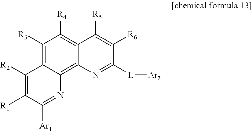


| TABLE 1 | ||||||
| second | fourth | |||||
| chemi- | chemi- | |||||
| first | cal | cal | ||||
| chemical | com- | com- | L1-H2 | L1-H3 | H2-H3 | |
| compound | pound | pound | (eV) | (eV) | (eV) | |
| Comparative | F4-TCNQ | NPD | ADN | 0.3 | 0.6 | 0.3 |
| Example 1 | (10%) | |||||
| Comparative | F4-TCNQ | D01 | ADN | −0.04 | 0.6 | 0.64 |
| Example 2 | (10%) | |||||
| Comparative | F4-TCNQ | D16 | ADN | −0.06 | 0.6 | 0.66 |
| Example 3 | (10%) | |||||
| Comparative | F4-TCNQ | D19 | ADN | −0.1 | 0.6 | 0.7 |
| Example 4 | (10%) | |||||
| Comparative | F4-TCNQ | D22 | ADN | −0.02 | 0.6 | 0.62 |
| Example 5 | (10%) | |||||
| Comparative | F4-TCNQ | D28 | ADN | −0.03 | 0.6 | 0.63 |
| Example 6 | (10%) | |||||
| Comparative | F4-TCNQ | D52 | ADN | 0.05 | 0.6 | 0.55 |
| Example 7 | (10%) | |||||
| Comparative | F4-TCNQ | 25 | ADN | 0.03 | 0.6 | 0.57 |
| Example 8 | (10%) | |||||
| Comparative | F4-TCNQ | 34 | ADN | −0.01 | 0.6 | 0.61 |
| Example 9 | (10%) | |||||
| Comparative | F4-TCNQ | 60 | ADN | 0 | 0.6 | 0.6 |
| Example 10 | (10%) | |||||
| Comparative | F4-TCNQ | 4-4 | ADN | 0.01 | 0.6 | 0.59 |
| Example 11 | (10%) | |||||
| Comparative | F4-TCNQ | 4-9 | ADN | 0.02 | 0.6 | 0.58 |
| Example 12 | (10%) | |||||
| Comparative | F4-TCNQ | 4-11 | ADN | −0.01 | 0.6 | 0.61 |
| Example 13 | (10%) | |||||
| Comparative | F4-TCNQ | 5-2 | ADN | 0 | 0.6 | 0.6 |
| Example 14 | (10%) | |||||
| Comparative | F4-TCNQ | 5-8 | ADN | 0 | 0.6 | 0.6 |
| Example 15 | (10%) | |||||
| Embodiment 1 | A04 (10%) | NPD | ADN | 0.75 | 1.05 | 0.3 |
| Embodiment 2 | A15 (10%) | D16 | ADN | 0.4 | 1.06 | 0.66 |
| Embodiment 3 | A15 (10%) | D19 | ADN | 0.36 | 1.06 | 0.7 |
| Embodiment 4 | A15 (10%) | D22 | ADN | 0.44 | 1.06 | 0.62 |
| Embodiment 5 | A15 (10%) | D28 | ADN | 0.45 | 1.06 | 0.63 |
| Embodiment 6 | A15 (10%) | D52 | ADN | 0.51 | 1.06 | 0.55 |
| Embodiment 7 | A38 (10%) | NPD | ADN | 0.7 | 1 | 0.3 |
| Embodiment 8 | A38 (10%) | D01 | ADN | 0.36 | 1 | 0.64 |
| Embodiment 9 | A38 (10%) | D16 | ADN | 0.34 | 1 | 0.66 |
| Embodiment 10 | A38 (10%) | D19 | ADN | 0.3 | 1 | 0.7 |
| Embodiment 11 | A38 (10%) | D22 | ADN | 0.38 | 1 | 0.62 |
| Embodiment 12 | A04 (10%) | D01 | ADN | 0.41 | 1.05 | 0.64 |
| Embodiment 13 | A38 (10%) | D28 | ADN | 0.39 | 1 | 0.63 |
| Embodiment 14 | A38 (10%) | D52 | ADN | 0.45 | 1 | 0.55 |
| Embodiment 15 | A04 (10%) | D16 | ADN | 0.39 | 1.05 | 0.66 |
| Embodiment 16 | A04 (10%) | D19 | ADN | 0.35 | 1.05 | 0.7 |
| Embodiment 17 | A04 (10%) | D22 | ADN | 0.43 | 1.05 | 0.62 |
| Embodiment 18 | A04 (10%) | D28 | ADN | 0.44 | 1.05 | 0.63 |
| Embodiment 19 | A04 (10%) | D52 | ADN | 0.5 | 1.05 | 0.55 |
| Embodiment 20 | A15 (10%) | NPD | ADN | 0.76 | 1.06 | 0.3 |
| Embodiment 21 | A15 (10%) | D01 | ADN | 0.42 | 1.06 | 0.64 |
| Embodiment 22 | A04 (10%) | NPD | ADN | 0.75 | 1.05 | 0.3 |
| Embodiment 23 | A38 (10%) | 25 | ADN | 0.43 | 1 | 0.57 |
| Embodiment 24 | A38 (10%) | 34 | ADN | 0.39 | 1 | 0.61 |
| Embodiment 25 | A38 (10%) | 60 | ADN | 0.4 | 1 | 0.6 |
| Embodiment 26 | A04 (10%) | 25 | ADN | 0.48 | 1.05 | 0.57 |
| Embodiment 27 | A04 (10%) | 34 | ADN | 0.44 | 1.05 | 0.61 |
| Embodiment 28 | A04 (10%) | 60 | ADN | 0.45 | 1.05 | 0.6 |
| Embodiment 29 | A15 (10%) | NPD | ADN | 0.76 | 1.06 | 0.3 |
| Embodiment 30 | A15 (10%) | 25 | ADN | 0.49 | 1.06 | 0.57 |
| Embodiment 31 | A15 (10%) | 34 | ADN | 0.45 | 1.06 | 0.61 |
| Embodiment 32 | A15 (10%) | 60 | ADN | 0.46 | 1.06 | 0.6 |
| Embodiment 33 | A38 (10%) | NPD | ADN | 0.7 | 1 | 0.3 |
| Embodiment 34 | A15 (10%) | NPD | ADN | 0.76 | 1.06 | 0.3 |
| Embodiment 35 | A38 (10%) | 4-11 | ADN | 0.39 | 1 | 0.61 |
| Embodiment 36 | A38 (10%) | 5-2 | ADN | 0.4 | 1 | 0.6 |
| Embodiment 37 | A38 (10%) | 5-8 | ADN | 0.4 | 1 | 0.6 |
| Embodiment 38 | A15 (10%) | 4-4 | ADN | 0.47 | 1.06 | 0.59 |
| Embodiment 39 | A15 (10%) | 4-9 | ADN | 0.48 | 1.06 | 0.58 |
| Embodiment 40 | A15 (10%) | 4-11 | ADN | 0.45 | 1.06 | 0.61 |
| Embodiment 41 | A15 (10%) | 5-2 | ADN | 0.46 | 1.06 | 0.6 |
| Embodiment 42 | A15 (10%) | 5-8 | ADN | 0.46 | 1.06 | 0.6 |
| Embodiment 43 | A38 (10%) | NPD | ADN | 0.7 | 1 | 0.3 |
| Embodiment 44 | A38 (10%) | 4-4 | ADN | 0.41 | 1 | 0.59 |
| Embodiment 45 | A38 (10%) | 4-9 | ADN | 0.42 | 1 | 0.58 |
| TABLE 2 | ||||
| driving | effi- | color | ||
| voltage | ciency | coordinate | lifespan | |
| (V) | (cd/A) | (CIE x, y) | (T95, hr) | |
| Comparative Example 1 | 4.74 | 5.51 | 0.138 | 0.097 | 83 |
| Comparative Example 2 | 4.7 | 5.54 | 0.139 | 0.098 | 94 |
| Comparative Example 3 | 4.68 | 5.84 | 0.14 | 0.097 | 64 |
| Comparative Example 4 | 4.69 | 5.79 | 0.139 | 0.096 | 71 |
| Comparative Example 5 | 4.7 | 5.53 | 0.139 | 0.098 | 80 |
| Comparative Example 6 | 4.71 | 5.48 | 0.139 | 0.096 | 45 |
| Comparative Example 7 | 4.85 | 5.44 | 0.138 | 0.095 | 49 |
| Comparative Example 8 | 4.8 | 5.33 | 0.139 | 0.098 | 80 |
| Comparative Example 9 | 4.63 | 5.42 | 0.14 | 0.099 | 110 |
| Comparative Example 10 | 4.62 | 5.49 | 0.139 | 0.1 | 118 |
| Comparative Example 11 | 4.69 | 5.72 | 0.139 | 0.098 | 85 |
| Comparative Example 12 | 4.7 | 5.68 | 0.141 | 0.099 | 96 |
| Comparative Example 13 | 4.64 | 5.75 | 0.14 | 0.1 | 101 |
| Comparative Example 14 | 4.7 | 5.69 | 0.139 | 0.099 | 88 |
| Comparative Example 15 | 4.68 | 5.76 | 0.139 | 0.098 | 90 |
| Embodiment 1 | 4.5 | 5.93 | 0.14 | 0.097 | 105 |
| Embodiment 2 | 4.2 | 6.24 | 0.14 | 0.099 | 164 |
| Embodiment 3 | 4.28 | 6.19 | 0.14 | 0.098 | 142 |
| Embodiment 4 | 4.09 | 6.32 | 0.14 | 0.099 | 169 |
| Embodiment 5 | 4.24 | 6.3 | 0.141 | 0.098 | 103 |
| Embodiment 6 | 4.35 | 6.18 | 0.14 | 0.097 | 147 |
| Embodiment 7 | 4.33 | 6.14 | 0.14 | 0.099 | 105 |
| Embodiment 8 | 4.18 | 6.1 | 0.139 | 0.097 | 121 |
| Embodiment 9 | 4.05 | 6.32 | 0.141 | 0.1 | 161 |
| Embodiment 10 | 4.21 | 6.17 | 0.14 | 0.098 | 133 |
| Embodiment 11 | 4.1 | 6.25 | 0.14 | 0.099 | 182 |
| Embodiment 12 | 4.42 | 6.04 | 0.139 | 0.097 | 113 |
| Embodiment 13 | 4.2 | 6.28 | 0.14 | 0.098 | 126 |
| Embodiment 14 | 4.29 | 6.1 | 0.139 | 0.098 | 140 |
| Embodiment 15 | 4.38 | 6.24 | 0.14 | 0.098 | 135 |
| Embodiment 16 | 4.32 | 6.12 | 0.139 | 0.099 | 119 |
| Embodiment 17 | 4.17 | 6.3 | 0.141 | 0.1 | 150 |
| Embodiment 18 | 4.23 | 6.15 | 0.14 | 0.099 | 122 |
| Embodiment 19 | 4.45 | 6.09 | 0.139 | 0.098 | 130 |
| Embodiment 20 | 4.4 | 6.08 | 0.139 | 0.099 | 114 |
| Embodiment 21 | 4.29 | 6.16 | 0.14 | 0.099 | 125 |
| Embodiment 22 | 4.58 | 5.64 | 0.141 | 0.099 | 138 |
| Embodiment 23 | 4.34 | 5.61 | 0.14 | 0.099 | 148 |
| Embodiment 24 | 4.27 | 5.79 | 0.139 | 0.099 | 174 |
| Embodiment 25 | 4.25 | 5.82 | 0.141 | 0.1 | 191 |
| Embodiment 26 | 4.52 | 5.7 | 0.14 | 0.098 | 161 |
| Embodiment 27 | 4.46 | 5.69 | 0.139 | 0.098 | 180 |
| Embodiment 28 | 4.45 | 5.72 | 0.139 | 0.098 | 180 |
| Embodiment 29 | 4.5 | 5.65 | 0.14 | 0.099 | 126 |
| Embodiment 30 | 4.39 | 5.69 | 0.14 | 0.1 | 164 |
| Embodiment 31 | 4.4 | 5.76 | 0.139 | 0.099 | 168 |
| Embodiment 32 | 4.35 | 5.81 | 0.14 | 0.098 | 172 |
| Embodiment 33 | 4.38 | 5.58 | 0.139 | 0.099 | 147 |
| Embodiment 34 | 4.57 | 5.95 | 0.14 | 0.097 | 126 |
| Embodiment 35 | 4.2 | 6.27 | 0.139 | 0.099 | 227 |
| Embodiment 36 | 4.21 | 6.22 | 0.139 | 0.098 | 215 |
| Embodiment 37 | 4.19 | 6.5 | 0.14 | 0.099 | 239 |
| Embodiment 38 | 4.41 | 6 | 0.14 | 0.098 | 171 |
| Embodiment 39 | 4.3 | 6.45 | 0.139 | 0.099 | 188 |
| Embodiment 40 | 4.22 | 6.22 | 0.14 | 0.1 | 176 |
| Embodiment 41 | 4.2 | 6.18 | 0.139 | 0.097 | 160 |
| Embodiment 42 | 4.24 | 6.44 | 0.14 | 0.097 | 192 |
| Embodiment 43 | 4.36 | 5.97 | 0.139 | 0.098 | 161 |
| Embodiment 44 | 4.27 | 6.02 | 0.141 | 0.099 | 218 |
| Embodiment 45 | 4.26 | 6.49 | 0.14 | 0.1 | 232 |
| TABLE 3 | ||||||||
| fourth | fifth | sixth | seventh | eighth | ||||
| chemical | compound | compound | compound | compound | L6-L4 | L6-H5 | L4-H5 | |
| compound | chemical | chemical | chemical | chemical | (eV) | (eV) | (eV) | |
| Comparative | F4-TCNQ (10%) | NPD | Bphen | F4-TCNQ | NPD | 2.2 | 2.5 | 0.3 |
| Example 16 | (10%) | |||||||
| Comparative | F4-TCNQ (10%) | D01 | Bphen | F4-TCNQ | D01 | 2.2 | 2.16 | −0.04 |
| Example 17 | (10%) | |||||||
| Comparative | F4-TCNQ (10%) | D16 | Bphen | F4-TCNQ | D16 | 2.2 | 2.14 | −0.06 |
| Example 18 | (10%) | |||||||
| Comparative | F4-TCNQ (10%) | D19 | Bphen | F4-TCNQ | D19 | 2.2 | 2.1 | −0.1 |
| Example 19 | (10%) | |||||||
| Comparative | F4-TCNQ (10%) | D22 | Bphen | F4-TCNQ | D22 | 2.2 | 2.18 | −0.02 |
| Example 20 | (10%) | |||||||
| Comparative | F4-TCNQ (10%) | D28 | Bphen | F4-TCNQ | D28 | 2.2 | 2.17 | −0.03 |
| Example 21 | (10%) | |||||||
| Comparative | F4-TCNQ (10%) | D52 | Bphen | F4-TCNQ | D52 | 2.2 | 2.25 | 0.05 |
| Example 22 | (10%) | |||||||
| Comparative | F4-TCNQ (10%) | 25 | Bphen | F4-TCNQ | 25 | 2.2 | 2.23 | 0.03 |
| Example 23 | (10%) | |||||||
| Comparative | F4-TCNQ (10%) | 34 | Bphen | F4-TCNQ | 34 | 2.2 | 2.19 | −0.01 |
| Example 24 | (10%) | |||||||
| Comparative | F4-TCNQ (10%) | 60 | Bphen | F4-TCNQ | 60 | 2.2 | 2.2 | 0 |
| Example 25 | (10%) | |||||||
| Comparative | F4-TCNQ (10%) | 4-4 | Bphen | F4-TCNQ | 43559 | 2.2 | 2.21 | 0.01 |
| Example 26 | (10%) | |||||||
| Comparative | F4-TCNQ (10%) | 4-9 | Bphen | F4-TCNQ | 43564 | 2.2 | 2.22 | 0.02 |
| Example 27 | (10%) | |||||||
| Comparative | F4-TCNQ (10%) | 4-11 | Bphen | F4-TCNQ | 43566 | 2.2 | 2.19 | −0.01 |
| Example 28 | (10%) | |||||||
| Comparative | F4-TCNQ (10%) | 5-2 | Bphen | F4-TCNQ | 43587 | 2.2 | 2.2 | 0 |
| Example 29 | (10%) | |||||||
| Comparative | F4-TCNQ (10%) | 5-8 | Bphen | F4-TCNQ | 43593 | 2.2 | 2.2 | 0 |
| Example 30 | (10%) | |||||||
| Embodiment 46 | A04 (10%) | NPD | Bphen | A04 (10%) | NPD | 1.75 | 2.5 | 0.75 |
| Embodiment 47 | A04 (10%) | D01 | Bphen | A04 (10%) | D01 | 1.75 | 2.16 | 0.41 |
| Embodiment 48 | A04 (10%) | D16 | Bphen | A04 (10%) | D16 | 1.75 | 2.14 | 0.39 |
| Embodiment 49 | A04 (10%) | D19 | Bphen | A04 (10%) | D19 | 1.75 | 2.1 | 0.35 |
| Embodiment 50 | A04 (10%) | D22 | Bphen | A04 (10%) | D22 | 1.75 | 2.18 | 0.43 |
| Embodiment 51 | A04 (10%) | D28 | Bphen | A04 (10%) | D28 | 1.75 | 2.17 | 0.44 |
| Embodiment 52 | A04 (10%) | D52 | Bphen | A04 (10%) | D52 | 1.75 | 2.25 | 0.5 |
| Embodiment 53 | A15 (10%) | NPD | Bphen | A15 (10%) | NPD | 1.74 | 2.5 | 0.76 |
| Embodiment 54 | A15 (10%) | D01 | Bphen | A15 (10%) | D01 | 1.74 | 2.16 | 0.42 |
| Embodiment 55 | A15 (10%) | D16 | Bphen | A15 (10%) | D16 | 1.74 | 2.14 | 0.4 |
| Embodiment 56 | A15 (10%) | D19 | Bphen | A15 (10%) | D19 | 1.74 | 2.1 | 0.36 |
| Embodiment 57 | A15 (10%) | D22 | Bphen | A15 (10%) | D22 | 1.74 | 2.18 | 0.44 |
| Embodiment 58 | A15 (10%) | D28 | Bphen | A15 (10%) | D28 | 1.74 | 2.17 | 0.45 |
| Embodiment 59 | A15 (10%) | D52 | Bphen | A15 (10%) | D52 | 1.74 | 2.25 | 0.51 |
| Embodiment 60 | A38 (10%) | NPD | Bphen | A38 (10%) | NPD | 1.8 | 2.5 | 0.7 |
| Embodiment 61 | A38 (10%) | D01 | Bphen | A38 (10%) | D01 | 1.8 | 2.16 | 0.36 |
| Embodiment 62 | A38 (10%) | D16 | Bphen | A38 (10%) | D16 | 1.8 | 2.14 | 0.34 |
| Embodiment 63 | A38 (10%) | D19 | Bphen | A38 (10%) | D19 | 1.8 | 2.1 | 0.3 |
| Embodiment 64 | A38 (10%) | D22 | Bphen | A38 (10%) | D22 | 1.8 | 2.18 | 0.38 |
| Embodiment 65 | A38 (10%) | D28 | Bphen | A38 (10%) | D28 | 1.8 | 2.17 | 0.39 |
| Embodiment 66 | A38 (10%) | D52 | Bphen | A38 (10%) | D52 | 1.8 | 2.25 | 0.45 |
| Embodiment 67 | A04 (10%) | NPD | E05 | A04 (10%) | NPD | 1.69 | 2.44 | 0.75 |
| Embodiment 68 | A04 (10%) | D16 | E05 | A04 (10%) | D16 | 1.69 | 2.08 | 0.39 |
| Embodiment 69 | A04 (10%) | D22 | E27 | A04 (10%) | D22 | 1.63 | 2.06 | 0.43 |
| Embodiment 70 | A15 (10%) | NPD | E05 | A15 (10%) | NPD | 1.68 | 2.44 | 0.76 |
| Embodiment 71 | A15 (10%) | D16 | E05 | A15 (10%) | D16 | 1.68 | 2.08 | 0.4 |
| Embodiment 72 | A15 (10%) | D22 | E27 | A15 (10%) | D22 | 1.62 | 2.06 | 0.44 |
| Embodiment 73 | A04 (10%) | NPD | Bphen | A04 (10%) | NPD | 1.75 | 2.5 | 0.75 |
| Embodiment 74 | A04 (10%) | 25 | Bphen | A04 (10%) | 25 | 1.75 | 2.23 | 0.48 |
| Embodiment 75 | A04 (10%) | 34 | Bphen | A04 (10%) | 34 | 1.75 | 2.19 | 0.44 |
| Embodiment 76 | A04 (10%) | 60 | Bphen | A04 (10%) | 60 | 1.75 | 2.2 | 0.45 |
| Embodiment 77 | A15 (10%) | NPD | Bphen | A15 (10%) | NPD | 1.74 | 2.5 | 0.76 |
| Embodiment 78 | A15 (10%) | 25 | Bphen | A15 (10%) | 25 | 1.74 | 2.23 | 0.49 |
| Embodiment 79 | A15 (10%) | 34 | Bphen | A15 (10%) | 34 | 1.74 | 2.19 | 0.45 |
| Embodiment 80 | A15 (10%) | 60 | Bphen | A15 (10%) | 60 | 1.74 | 2.2 | 0.46 |
| Embodiment 81 | A38 (10%) | NPD | Bphen | A38 (10%) | NPD | 1.8 | 2.5 | 0.3 |
| Embodiment 82 | A38 (10%) | 25 | Bphen | A38 (10%) | 25 | 1.8 | 2.23 | 0.57 |
| Embodiment 83 | A38 (10%) | 34 | Bphen | A38 (10%) | 34 | 1.8 | 2.19 | 0.61 |
| Embodiment 84 | A38 (10%) | 60 | Bphen | A38 (10%) | 60 | 1.8 | 2.2 | 0.6 |
| Embodiment 85 | A15 (10%) | NPD | E05 | A15 (10%) | NPD | 1.68 | 2.44 | 0.76 |
| Embodiment 86 | A15 (10%) | 25 | E05 | A15 (10%) | 25 | 1.68 | 2.17 | 0.49 |
| Embodiment 87 | A15 (10%) | 34 | E27 | A15 (10%) | 34 | 1.62 | 2.07 | 0.45 |
| Embodiment 88 | A38 (10%) | NPD | E05 | A38 (10%) | NPD | 1.74 | 2.44 | 0.7 |
| Embodiment 89 | A38 (10%) | 25 | E05 | A38 (10%) | 25 | 1.74 | 2.17 | 0.57 |
| Embodiment 90 | A38 (10%) | 34 | E27 | A38 (10%) | 34 | 1.68 | 2.07 | 0.61 |
| Embodiment 91 | A15 (10%) | NPD | Bphen | A15 (10%) | NPD | 1.74 | 2.5 | 0.76 |
| Embodiment 92 | A15 (10%) | 4-4 | Bphen | A15 (10%) | 43559 | 1.74 | 2.21 | 0.47 |
| Embodiment 93 | A15 (10%) | 4-9 | Bphen | A15 (10%) | 43564 | 1.74 | 2.22 | 0.48 |
| Embodiment 94 | A15 (10%) | 4-11 | Bphen | A15 (10%) | 43566 | 1.74 | 2.19 | 0.45 |
| Embodiment 95 | A15 (10%) | 5-2 | Bphen | A15 (10%) | 43587 | 1.74 | 2.2 | 0.46 |
| Embodiment 96 | A15 (10%) | 5-8 | Bphen | A15 (10%) | 43593 | 1.74 | 2.2 | 0.46 |
| Embodiment 97 | A38 (10%) | NPD | Bphen | A38 (10%) | NPD | 1.8 | 2.5 | 0.7 |
| Embodiment 98 | A38 (10%) | 4-4 | Bphen | A38 (10%) | 43559 | 1.8 | 2.21 | 0.41 |
| Embodiment 99 | A38 (10%) | 4-9 | Bphen | A38 (10%) | 43564 | 1.8 | 2.22 | 0.42 |
| Embodiment | A38 (10%) | 4-11 | Bphen | A38 (10%) | 43566 | 1.8 | 2.19 | 0.39 |
| 100 | ||||||||
| Embodiment | A38 (10%) | 5-2 | Bphen | A38 (10%) | 43587 | 1.8 | 2.2 | 0.4 |
| 101 | ||||||||
| Embodiment | A38 (10%) | 5-8 | Bphen | A38 (10%) | 43593 | 1.8 | 2.2 | 0.4 |
| 102 | ||||||||
| Embodiment | A15 (10%) | NPD | E05 | A15 (10%) | NPD | 1.68 | 2.44 | 0.76 |
| 103 | ||||||||
| Embodiment | A15 (10%) | 4-11 | E05 | A15 (10%) | 4-11 | 1.68 | 2.19 | 0.45 |
| 104 | ||||||||
| Embodiment | A15 (10%) | 5-8 | E27 | A15 (10%) | 5-8 | 1.62 | 2.2 | 0.4 |
| 105 | ||||||||
| Embodiment | A38 (10%) | NPD | E05 | A38 (10%) | NPD | 1.74 | 2.44 | 0.7 |
| 106 | ||||||||
| Embodiment | A38 (10%) | 4-11 | E05 | A38 (10%) | 4-11 | 1.74 | 2.19 | 0.39 |
| 107 | ||||||||
| Embodiment | A38 (10%) | 5-8 | E27 | A38 (10%) | 5-8 | 1.68 | 2.2 | 0.4 |
| 108 | ||||||||
| TABLE 4 | ||||
| driving | effi- | color | ||
| voltage | ciency | coordinate | lifespan | |
| (V) | (cd/A) | (CIE x, y) | (T95, hr) | |
| Comparative Example 16 | 10.6 | 56.1 | 0.317 | 0.33 | 283 |
| Comparative Example 17 | 10.4 | 56.4 | 0.32 | 0.345 | 294 |
| Comparative Example 18 | 9.8 | 59.4 | 0.323 | 0.34 | 264 |
| Comparative Example 19 | 9.9 | 58.9 | 0.321 | 0.336 | 271 |
| Comparative Example 20 | 10.2 | 56.3 | 0.318 | 0.344 | 280 |
| Comparative Example 21 | 10.2 | 55.8 | 0.325 | 0.342 | 245 |
| Comparative Example 22 | 11.3 | 55.4 | 0.319 | 0.344 | 249 |
| Comparative Example 23 | 10.4 | 53.3 | 0.32 | 0.331 | 280 |
| Comparative Example 24 | 9.7 | 54.2 | 0.319 | 0.336 | 330 |
| Comparative Example 25 | 9.9 | 54.9 | 0.32 | 0.333 | 328 |
| Comparative Example 26 | 10.2 | 57.2 | 0.32 | 0.334 | 315 |
| Comparative Example 27 | 10.5 | 56.8 | 0.318 | 0.329 | 346 |
| Comparative Example 28 | 9.8 | 57.5 | 0.322 | 0.336 | 351 |
| Comparative Example 29 | 10.2 | 56.9 | 0.325 | 0.333 | 338 |
| Comparative Example 30 | 10.1 | 57.6 | 0.321 | 0.34 | 340 |
| Embodiment 46 | 9.5 | 60.3 | 0.322 | 0.339 | 305 |
| Embodiment 47 | 9.2 | 61.4 | 0.32 | 0.34 | 313 |
| Embodiment 48 | 8.7 | 63.4 | 0.325 | 0.338 | 335 |
| Embodiment 49 | 9 | 62.2 | 0.323 | 0.335 | 319 |
| Embodiment 50 | 8.4 | 64 | 0.327 | 0.341 | 350 |
| Embodiment 51 | 8.8 | 62.5 | 0.319 | 0.34 | 322 |
| Embodiment 52 | 9.4 | 61.9 | 0.32 | 0.343 | 330 |
| Embodiment 53 | 9.3 | 61.8 | 0.326 | 0.339 | 314 |
| Embodiment 54 | 9.2 | 62.6 | 0.325 | 0.341 | 325 |
| Embodiment 55 | 8.5 | 63.4 | 0.324 | 0.34 | 364 |
| Embodiment 56 | 8.9 | 62.9 | 0.322 | 0.337 | 342 |
| Embodiment 57 | 8.2 | 64.2 | 0.319 | 0.341 | 369 |
| Embodiment 58 | 8.7 | 64 | 0.321 | 0.34 | 303 |
| Embodiment 59 | 9.1 | 62.8 | 0.323 | 0.342 | 347 |
| Embodiment 60 | 9.1 | 62.4 | 0.32 | 0.338 | 305 |
| Embodiment 61 | 9.2 | 62 | 0.319 | 0.335 | 321 |
| Embodiment 62 | 8 | 64.2 | 0.322 | 0.339 | 361 |
| Embodiment 63 | 8.7 | 62.7 | 0.323 | 0.337 | 333 |
| Embodiment 64 | 8.1 | 63.5 | 0.32 | 0.341 | 382 |
| Embodiment 65 | 8.6 | 63.8 | 0.324 | 0.344 | 326 |
| Embodiment 66 | 9 | 63 | 0.323 | 0.343 | 340 |
| Embodiment 67 | 9.1 | 62.7 | 0.326 | 0.331 | 310 |
| Embodiment 68 | 8.7 | 63.4 | 0.319 | 0.338 | 335 |
| Embodiment 69 | 8.4 | 64 | 0.327 | 0.341 | 350 |
| Embodiment 70 | 8.9 | 63 | 0.321 | 0.331 | 341 |
| Embodiment 71 | 8.5 | 63.4 | 0.317 | 0.34 | 364 |
| Embodiment 72 | 8.2 | 64.2 | 0.319 | 0.341 | 369 |
| Embodiment 73 | 9.4 | 56.4 | 0.323 | 0.335 | 338 |
| Embodiment 74 | 9 | 57 | 0.323 | 0.334 | 361 |
| Embodiment 75 | 8.6 | 56.9 | 0.322 | 0.332 | 380 |
| Embodiment 76 | 8.8 | 57.2 | 0.32 | 0.331 | 380 |
| Embodiment 77 | 9.3 | 56.5 | 0.321 | 0.334 | 326 |
| Embodiment 78 | 9 | 56.9 | 0.321 | 0.331 | 364 |
| Embodiment 79 | 8.4 | 57.6 | 0.322 | 0.332 | 368 |
| Embodiment 80 | 8.8 | 58.1 | 0.318 | 0.33 | 372 |
| Embodiment 81 | 9.2 | 55.8 | 0.318 | 0.338 | 347 |
| Embodiment 82 | 8.8 | 56.1 | 0.318 | 0.33 | 348 |
| Embodiment 83 | 8.4 | 57.9 | 0.321 | 0.334 | 374 |
| Embodiment 84 | 8.3 | 58.2 | 0.326 | 0.333 | 391 |
| Embodiment 85 | 9 | 60.3 | 0.323 | 0.337 | 453 |
| Embodiment 86 | 8.4 | 57.6 | 0.322 | 0.332 | 368 |
| Embodiment 87 | 9.1 | 57.4 | 0.32 | 0.335 | 383 |
| Embodiment 88 | 8.9 | 56.2 | 0.32 | 0.334 | 353 |
| Embodiment 89 | 8.4 | 57.9 | 0.321 | 0.334 | 374 |
| Embodiment 90 | 8.8 | 57.1 | 0.323 | 0.335 | 384 |
| Embodiment 91 | 9.6 | 59.5 | 0.324 | 0.339 | 426 |
| Embodiment 92 | 9.1 | 60 | 0.32 | 0.347 | 521 |
| Embodiment 93 | 8.8 | 64.5 | 0.315 | 0.338 | 538 |
| Embodiment 94 | 8.3 | 62.2 | 0.322 | 0.331 | 526 |
| Embodiment 95 | 8.2 | 61.8 | 0.322 | 0.342 | 510 |
| Embodiment 96 | 8.4 | 64.4 | 0.321 | 0.341 | 542 |
| Embodiment 97 | 9.5 | 59.7 | 0.321 | 0.34 | 461 |
| Embodiment 98 | 8.9 | 60.2 | 0.321 | 0.342 | 518 |
| Embodiment 99 | 8.6 | 64.9 | 0.32 | 0.34 | 532 |
| Embodiment 100 | 8.2 | 62.7 | 0.322 | 0.341 | 527 |
| Embodiment 101 | 8.2 | 62.2 | 0.322 | 0.343 | 515 |
| Embodiment 102 | 8.3 | 65 | 0.321 | 0.34 | 539 |
| Embodiment 103 | 9 | 60.3 | 0.323 | 0.337 | 453 |
| Embodiment 104 | 8.3 | 62.2 | 0.322 | 0.331 | 526 |
| Embodiment 105 | 8.4 | 64.4 | 0.321 | 0.345 | 542 |
| Embodiment 106 | 8.9 | 63 | 0.321 | 0.331 | 341 |
| Embodiment 107 | 8.2 | 62.7 | 0.322 | 0.342 | 527 |
| Embodiment 108 | 8.2 | 65 | 0.321 | 0.34 | 539 |
Claims (12)
0.32 eV≤L 1 −H 2≤0.8 eV [general formula 1]
0.80 eV≤L 1 −H 3≤1.4 eV [general formula 2]
0.40 eV≤H 2 −H 3≤0.9 eV [general formula 3]
L 6 −L 4≤2.1 eV [general formula 4]
L 6 −H 5≤2.8 eV [general formula 5]
0.32 eV≤L 4 −H 5≤0.8 eV [general formula 6]
Priority Applications (1)
| Application Number | Priority Date | Filing Date | Title |
|---|---|---|---|
| US18/207,400 US20240040812A1 (en) | 2019-12-31 | 2023-06-08 | Organic electric element, display panel comprising the same and display device comprising the same |
Applications Claiming Priority (2)
| Application Number | Priority Date | Filing Date | Title |
|---|---|---|---|
| KR10-2019-0180011 | 2019-12-31 | ||
| KR1020190180011A KR102826051B1 (en) | 2019-12-31 | 2019-12-31 | Organic electronic element, display panel comprising the same and display device comprising the same |
Related Child Applications (1)
| Application Number | Title | Priority Date | Filing Date |
|---|---|---|---|
| US18/207,400 Continuation US20240040812A1 (en) | 2019-12-31 | 2023-06-08 | Organic electric element, display panel comprising the same and display device comprising the same |
Publications (2)
| Publication Number | Publication Date |
|---|---|
| US20210202872A1 US20210202872A1 (en) | 2021-07-01 |
| US11716865B2 true US11716865B2 (en) | 2023-08-01 |
Family
ID=74003738
Family Applications (2)
| Application Number | Title | Priority Date | Filing Date |
|---|---|---|---|
| US17/138,226 Active 2041-07-30 US11716865B2 (en) | 2019-12-31 | 2020-12-30 | Organic electric element, display panel comprising the same and display device comprising the same |
| US18/207,400 Pending US20240040812A1 (en) | 2019-12-31 | 2023-06-08 | Organic electric element, display panel comprising the same and display device comprising the same |
Family Applications After (1)
| Application Number | Title | Priority Date | Filing Date |
|---|---|---|---|
| US18/207,400 Pending US20240040812A1 (en) | 2019-12-31 | 2023-06-08 | Organic electric element, display panel comprising the same and display device comprising the same |
Country Status (4)
| Country | Link |
|---|---|
| US (2) | US11716865B2 (en) |
| EP (2) | EP4216697B1 (en) |
| KR (2) | KR102826051B1 (en) |
| CN (2) | CN118317619A (en) |
Families Citing this family (3)
| Publication number | Priority date | Publication date | Assignee | Title |
|---|---|---|---|---|
| EP4199131A1 (en) | 2021-12-15 | 2023-06-21 | Novaled GmbH | A ce(iv) metal complex, an organic electronic device comprising an anode layer, a cathode layer and a charge generation layer, wherein the charge generation layer comprises a p-type charge generation layer that comprises the ce(iv) metal complex and a n-type charge generation layer |
| KR102900364B1 (en) * | 2021-12-31 | 2025-12-15 | 엘지디스플레이 주식회사 | Light Emitting Element and Display Device Using the Same |
| KR20240168762A (en) * | 2023-05-23 | 2024-12-02 | 삼성에스디아이 주식회사 | Organic optoelectronic device and display device |
Citations (8)
| Publication number | Priority date | Publication date | Assignee | Title |
|---|---|---|---|---|
| US20130264551A1 (en) | 2012-04-05 | 2013-10-10 | Lg Display Co., Ltd. | Tandem White Organic Light Emitting Device |
| EP2889929A1 (en) | 2013-12-31 | 2015-07-01 | LG Display Co., Ltd. | White organic light emitting device |
| CN105161637A (en) | 2015-08-17 | 2015-12-16 | Tcl集团股份有限公司 | Quantum dot light emitting diode containing doped hole injection layer and fabrication method of quantum dot light emitting diode |
| US20160343776A1 (en) * | 2015-05-23 | 2016-11-24 | Lg Display Co., Ltd. | Organic Light Emitting Device |
| US20170162792A1 (en) * | 2015-12-03 | 2017-06-08 | Lg Display Co., Ltd. | Organic light emitting display device |
| US20180033373A1 (en) * | 2016-07-28 | 2018-02-01 | Lg Display Co., Ltd. | Organic light-emitting display panel, organic light-emitting display device, driving circuit, controller, and driving method |
| US20190036055A1 (en) * | 2017-07-26 | 2019-01-31 | Universal Display Corporation | Organic electroluminescent materials and devices |
| US20200266375A1 (en) * | 2018-09-18 | 2020-08-20 | Yungu (Gu'an) Technology Co., Ltd. | Organic light-emitting diode and display panel |
Family Cites Families (2)
| Publication number | Priority date | Publication date | Assignee | Title |
|---|---|---|---|---|
| KR102086890B1 (en) * | 2017-05-31 | 2020-03-09 | 주식회사 엘지화학 | Organic light emitting device |
| KR102486441B1 (en) * | 2017-12-28 | 2023-01-06 | 엘지디스플레이 주식회사 | Organic light emitting diode |
-
2019
- 2019-12-31 KR KR1020190180011A patent/KR102826051B1/en active Active
-
2020
- 2020-12-11 CN CN202410305587.0A patent/CN118317619A/en active Pending
- 2020-12-11 CN CN202011449760.2A patent/CN113130800B/en active Active
- 2020-12-29 EP EP23161534.5A patent/EP4216697B1/en active Active
- 2020-12-29 EP EP20217567.5A patent/EP3846234B1/en active Active
- 2020-12-30 US US17/138,226 patent/US11716865B2/en active Active
-
2023
- 2023-06-08 US US18/207,400 patent/US20240040812A1/en active Pending
-
2025
- 2025-06-23 KR KR1020250082559A patent/KR20250105324A/en active Pending
Patent Citations (8)
| Publication number | Priority date | Publication date | Assignee | Title |
|---|---|---|---|---|
| US20130264551A1 (en) | 2012-04-05 | 2013-10-10 | Lg Display Co., Ltd. | Tandem White Organic Light Emitting Device |
| EP2889929A1 (en) | 2013-12-31 | 2015-07-01 | LG Display Co., Ltd. | White organic light emitting device |
| US20160343776A1 (en) * | 2015-05-23 | 2016-11-24 | Lg Display Co., Ltd. | Organic Light Emitting Device |
| CN105161637A (en) | 2015-08-17 | 2015-12-16 | Tcl集团股份有限公司 | Quantum dot light emitting diode containing doped hole injection layer and fabrication method of quantum dot light emitting diode |
| US20170162792A1 (en) * | 2015-12-03 | 2017-06-08 | Lg Display Co., Ltd. | Organic light emitting display device |
| US20180033373A1 (en) * | 2016-07-28 | 2018-02-01 | Lg Display Co., Ltd. | Organic light-emitting display panel, organic light-emitting display device, driving circuit, controller, and driving method |
| US20190036055A1 (en) * | 2017-07-26 | 2019-01-31 | Universal Display Corporation | Organic electroluminescent materials and devices |
| US20200266375A1 (en) * | 2018-09-18 | 2020-08-20 | Yungu (Gu'an) Technology Co., Ltd. | Organic light-emitting diode and display panel |
Non-Patent Citations (1)
| Title |
|---|
| Extended European Search Report dated May 28, 2021, issued in corresponding European Patent Application No. 20217567.5. |
Also Published As
| Publication number | Publication date |
|---|---|
| CN113130800B (en) | 2024-04-05 |
| CN118317619A (en) | 2024-07-09 |
| KR102826051B1 (en) | 2025-06-27 |
| US20210202872A1 (en) | 2021-07-01 |
| US20240040812A1 (en) | 2024-02-01 |
| EP3846234B1 (en) | 2023-03-29 |
| EP4216697B1 (en) | 2025-12-17 |
| EP3846234A1 (en) | 2021-07-07 |
| KR20250105324A (en) | 2025-07-08 |
| EP4216697A1 (en) | 2023-07-26 |
| KR20210086219A (en) | 2021-07-08 |
| CN113130800A (en) | 2021-07-16 |
Similar Documents
| Publication | Publication Date | Title |
|---|---|---|
| US20250063942A1 (en) | Organic electric element, display panel comprising the same and display device comprising the same | |
| US11997919B2 (en) | Organic electric element, display panel comprising the same and display device comprising the same | |
| US20240040812A1 (en) | Organic electric element, display panel comprising the same and display device comprising the same | |
| EP3846239B1 (en) | Organic electric element, display panel comprising the same and display device comprising the same | |
| US12349590B2 (en) | Organic electric element, display panel comprising the same and display device comprising the same | |
| EP3846242B1 (en) | Organic electric element, display panel comprising the same and display device comprising the same | |
| US12364158B2 (en) | Organic electric element, display panel comprising the same and display device comprising the same | |
| US11430964B2 (en) | Organic electric element, display panel comprising the same and display device comprising the same |
Legal Events
| Date | Code | Title | Description |
|---|---|---|---|
| AS | Assignment |
Owner name: LG DISPLAY CO., LTD., KOREA, REPUBLIC OF Free format text: ASSIGNMENT OF ASSIGNORS INTEREST;ASSIGNORS:SHIN, JICHEOL;YOO, SEONKEUN;SEO, JEONGDAE;AND OTHERS;SIGNING DATES FROM 20201207 TO 20201211;REEL/FRAME:054780/0539 Owner name: LG CHEM, LTD., KOREA, REPUBLIC OF Free format text: ASSIGNMENT OF ASSIGNORS INTEREST;ASSIGNORS:SHIN, JICHEOL;YOO, SEONKEUN;SEO, JEONGDAE;AND OTHERS;SIGNING DATES FROM 20201207 TO 20201211;REEL/FRAME:054780/0539 |
|
| FEPP | Fee payment procedure |
Free format text: ENTITY STATUS SET TO UNDISCOUNTED (ORIGINAL EVENT CODE: BIG.); ENTITY STATUS OF PATENT OWNER: LARGE ENTITY |
|
| STPP | Information on status: patent application and granting procedure in general |
Free format text: APPLICATION DISPATCHED FROM PREEXAM, NOT YET DOCKETED |
|
| STPP | Information on status: patent application and granting procedure in general |
Free format text: DOCKETED NEW CASE - READY FOR EXAMINATION |
|
| STPP | Information on status: patent application and granting procedure in general |
Free format text: NON FINAL ACTION MAILED |
|
| STPP | Information on status: patent application and granting procedure in general |
Free format text: RESPONSE TO NON-FINAL OFFICE ACTION ENTERED AND FORWARDED TO EXAMINER |
|
| STPP | Information on status: patent application and granting procedure in general |
Free format text: PUBLICATIONS -- ISSUE FEE PAYMENT VERIFIED |
|
| STCF | Information on status: patent grant |
Free format text: PATENTED CASE |