US11670551B2 - Interface trap charge density reduction - Google Patents
Interface trap charge density reduction Download PDFInfo
- Publication number
- US11670551B2 US11670551B2 US16/926,528 US202016926528A US11670551B2 US 11670551 B2 US11670551 B2 US 11670551B2 US 202016926528 A US202016926528 A US 202016926528A US 11670551 B2 US11670551 B2 US 11670551B2
- Authority
- US
- United States
- Prior art keywords
- fin
- silicon
- forming
- layer
- cap layer
- Prior art date
- Legal status (The legal status is an assumption and is not a legal conclusion. Google has not performed a legal analysis and makes no representation as to the accuracy of the status listed.)
- Active, expires
Links
- 230000009467 reduction Effects 0.000 title description 5
- 230000005527 interface trap Effects 0.000 title description 4
- 238000000034 method Methods 0.000 claims abstract description 165
- 239000004065 semiconductor Substances 0.000 claims abstract description 90
- 239000000463 material Substances 0.000 claims abstract description 67
- 239000000758 substrate Substances 0.000 claims abstract description 31
- 238000000137 annealing Methods 0.000 claims abstract description 8
- 229910052710 silicon Inorganic materials 0.000 claims description 106
- XUIMIQQOPSSXEZ-UHFFFAOYSA-N Silicon Chemical compound [Si] XUIMIQQOPSSXEZ-UHFFFAOYSA-N 0.000 claims description 104
- 239000010703 silicon Substances 0.000 claims description 104
- 229910052751 metal Inorganic materials 0.000 claims description 38
- 239000002184 metal Substances 0.000 claims description 38
- 108091006146 Channels Proteins 0.000 claims description 34
- 238000000231 atomic layer deposition Methods 0.000 claims description 20
- 238000002955 isolation Methods 0.000 claims description 19
- 238000000151 deposition Methods 0.000 claims description 18
- 229910052732 germanium Inorganic materials 0.000 claims description 16
- GNPVGFCGXDBREM-UHFFFAOYSA-N germanium atom Chemical compound [Ge] GNPVGFCGXDBREM-UHFFFAOYSA-N 0.000 claims description 16
- 238000005530 etching Methods 0.000 claims description 13
- VYPSYNLAJGMNEJ-UHFFFAOYSA-N Silicium dioxide Chemical compound O=[Si]=O VYPSYNLAJGMNEJ-UHFFFAOYSA-N 0.000 claims description 10
- 229910052814 silicon oxide Inorganic materials 0.000 claims description 10
- VXEGSRKPIUDPQT-UHFFFAOYSA-N 4-[4-(4-methoxyphenyl)piperazin-1-yl]aniline Chemical compound C1=CC(OC)=CC=C1N1CCN(C=2C=CC(N)=CC=2)CC1 VXEGSRKPIUDPQT-UHFFFAOYSA-N 0.000 claims description 8
- 239000005049 silicon tetrachloride Substances 0.000 claims description 8
- ZDHXKXAHOVTTAH-UHFFFAOYSA-N trichlorosilane Chemical compound Cl[SiH](Cl)Cl ZDHXKXAHOVTTAH-UHFFFAOYSA-N 0.000 claims description 8
- 239000005052 trichlorosilane Substances 0.000 claims description 8
- 108010075750 P-Type Calcium Channels Proteins 0.000 claims description 7
- BLRPTPMANUNPDV-UHFFFAOYSA-N Silane Chemical compound [SiH4] BLRPTPMANUNPDV-UHFFFAOYSA-N 0.000 claims description 7
- 150000004767 nitrides Chemical class 0.000 claims description 6
- 108090000699 N-Type Calcium Channels Proteins 0.000 claims description 4
- 102000004129 N-Type Calcium Channels Human genes 0.000 claims description 4
- MROCJMGDEKINLD-UHFFFAOYSA-N dichlorosilane Chemical compound Cl[SiH2]Cl MROCJMGDEKINLD-UHFFFAOYSA-N 0.000 claims description 3
- 229910000077 silane Inorganic materials 0.000 claims description 3
- 229910021420 polycrystalline silicon Inorganic materials 0.000 claims description 2
- 229920005591 polysilicon Polymers 0.000 claims description 2
- 239000010410 layer Substances 0.000 description 144
- 230000008569 process Effects 0.000 description 114
- 239000007789 gas Substances 0.000 description 21
- 230000015572 biosynthetic process Effects 0.000 description 18
- 230000006870 function Effects 0.000 description 14
- 239000003989 dielectric material Substances 0.000 description 12
- IJGRMHOSHXDMSA-UHFFFAOYSA-N Atomic nitrogen Chemical compound N#N IJGRMHOSHXDMSA-UHFFFAOYSA-N 0.000 description 10
- QVGXLLKOCUKJST-UHFFFAOYSA-N atomic oxygen Chemical compound [O] QVGXLLKOCUKJST-UHFFFAOYSA-N 0.000 description 10
- 229910052760 oxygen Inorganic materials 0.000 description 10
- 239000001301 oxygen Substances 0.000 description 10
- 229910052581 Si3N4 Inorganic materials 0.000 description 9
- 229910000577 Silicon-germanium Inorganic materials 0.000 description 9
- 238000000059 patterning Methods 0.000 description 9
- 238000005229 chemical vapour deposition Methods 0.000 description 8
- 238000004519 manufacturing process Methods 0.000 description 8
- 239000002019 doping agent Substances 0.000 description 7
- 230000005669 field effect Effects 0.000 description 7
- 230000003647 oxidation Effects 0.000 description 7
- 238000007254 oxidation reaction Methods 0.000 description 7
- HQVNEWCFYHHQES-UHFFFAOYSA-N silicon nitride Chemical compound N12[Si]34N5[Si]62N3[Si]51N64 HQVNEWCFYHHQES-UHFFFAOYSA-N 0.000 description 7
- 229910052757 nitrogen Inorganic materials 0.000 description 6
- 229910021332 silicide Inorganic materials 0.000 description 6
- FVBUAEGBCNSCDD-UHFFFAOYSA-N silicide(4-) Chemical compound [Si-4] FVBUAEGBCNSCDD-UHFFFAOYSA-N 0.000 description 6
- 239000010936 titanium Substances 0.000 description 6
- NRTOMJZYCJJWKI-UHFFFAOYSA-N Titanium nitride Chemical compound [Ti]#N NRTOMJZYCJJWKI-UHFFFAOYSA-N 0.000 description 5
- 229910052782 aluminium Inorganic materials 0.000 description 5
- 230000004888 barrier function Effects 0.000 description 5
- 239000004020 conductor Substances 0.000 description 5
- 239000001257 hydrogen Substances 0.000 description 5
- 229910052739 hydrogen Inorganic materials 0.000 description 5
- 239000012212 insulator Substances 0.000 description 5
- 229910052719 titanium Inorganic materials 0.000 description 5
- LEVVHYCKPQWKOP-UHFFFAOYSA-N [Si].[Ge] Chemical compound [Si].[Ge] LEVVHYCKPQWKOP-UHFFFAOYSA-N 0.000 description 4
- 230000008901 benefit Effects 0.000 description 4
- 125000001309 chloro group Chemical group Cl* 0.000 description 4
- 239000000470 constituent Substances 0.000 description 4
- 230000007547 defect Effects 0.000 description 4
- 238000009792 diffusion process Methods 0.000 description 4
- 238000001459 lithography Methods 0.000 description 4
- PXHVJJICTQNCMI-UHFFFAOYSA-N nickel Substances [Ni] PXHVJJICTQNCMI-UHFFFAOYSA-N 0.000 description 4
- 230000005855 radiation Effects 0.000 description 4
- 229910052715 tantalum Inorganic materials 0.000 description 4
- MZLGASXMSKOWSE-UHFFFAOYSA-N tantalum nitride Chemical compound [Ta]#N MZLGASXMSKOWSE-UHFFFAOYSA-N 0.000 description 4
- UFHFLCQGNIYNRP-UHFFFAOYSA-N Hydrogen Chemical compound [H][H] UFHFLCQGNIYNRP-UHFFFAOYSA-N 0.000 description 3
- 229910003818 SiH2Cl2 Inorganic materials 0.000 description 3
- 239000010949 copper Substances 0.000 description 3
- 230000008021 deposition Effects 0.000 description 3
- 239000003292 glue Substances 0.000 description 3
- 229910044991 metal oxide Inorganic materials 0.000 description 3
- 150000004706 metal oxides Chemical class 0.000 description 3
- 229910052759 nickel Inorganic materials 0.000 description 3
- 238000000206 photolithography Methods 0.000 description 3
- 239000000376 reactant Substances 0.000 description 3
- 125000006850 spacer group Chemical group 0.000 description 3
- 229910052721 tungsten Inorganic materials 0.000 description 3
- 229910052726 zirconium Inorganic materials 0.000 description 3
- ZOXJGFHDIHLPTG-UHFFFAOYSA-N Boron Chemical compound [B] ZOXJGFHDIHLPTG-UHFFFAOYSA-N 0.000 description 2
- OKTJSMMVPCPJKN-UHFFFAOYSA-N Carbon Chemical compound [C] OKTJSMMVPCPJKN-UHFFFAOYSA-N 0.000 description 2
- KDLHZDBZIXYQEI-UHFFFAOYSA-N Palladium Chemical compound [Pd] KDLHZDBZIXYQEI-UHFFFAOYSA-N 0.000 description 2
- OAICVXFJPJFONN-UHFFFAOYSA-N Phosphorus Chemical compound [P] OAICVXFJPJFONN-UHFFFAOYSA-N 0.000 description 2
- GWEVSGVZZGPLCZ-UHFFFAOYSA-N Titan oxide Chemical compound O=[Ti]=O GWEVSGVZZGPLCZ-UHFFFAOYSA-N 0.000 description 2
- RTAQQCXQSZGOHL-UHFFFAOYSA-N Titanium Chemical compound [Ti] RTAQQCXQSZGOHL-UHFFFAOYSA-N 0.000 description 2
- QCWXUUIWCKQGHC-UHFFFAOYSA-N Zirconium Chemical compound [Zr] QCWXUUIWCKQGHC-UHFFFAOYSA-N 0.000 description 2
- MCMNRKCIXSYSNV-UHFFFAOYSA-N Zirconium dioxide Chemical compound O=[Zr]=O MCMNRKCIXSYSNV-UHFFFAOYSA-N 0.000 description 2
- PNEYBMLMFCGWSK-UHFFFAOYSA-N aluminium oxide Inorganic materials [O-2].[O-2].[O-2].[Al+3].[Al+3] PNEYBMLMFCGWSK-UHFFFAOYSA-N 0.000 description 2
- 229910052796 boron Inorganic materials 0.000 description 2
- 229910052799 carbon Inorganic materials 0.000 description 2
- 229910017052 cobalt Inorganic materials 0.000 description 2
- 239000010941 cobalt Substances 0.000 description 2
- GUTLYIVDDKVIGB-UHFFFAOYSA-N cobalt atom Chemical compound [Co] GUTLYIVDDKVIGB-UHFFFAOYSA-N 0.000 description 2
- 229910052802 copper Inorganic materials 0.000 description 2
- 229910052593 corundum Inorganic materials 0.000 description 2
- 230000008878 coupling Effects 0.000 description 2
- 238000010168 coupling process Methods 0.000 description 2
- 238000005859 coupling reaction Methods 0.000 description 2
- 230000006378 damage Effects 0.000 description 2
- 238000011161 development Methods 0.000 description 2
- 230000018109 developmental process Effects 0.000 description 2
- 238000002408 directed self-assembly Methods 0.000 description 2
- 238000000226 double patterning lithography Methods 0.000 description 2
- 230000000694 effects Effects 0.000 description 2
- 238000005516 engineering process Methods 0.000 description 2
- 238000010438 heat treatment Methods 0.000 description 2
- 150000002431 hydrogen Chemical class 0.000 description 2
- 239000011229 interlayer Substances 0.000 description 2
- 229910052698 phosphorus Inorganic materials 0.000 description 2
- 239000011574 phosphorus Substances 0.000 description 2
- 238000001020 plasma etching Methods 0.000 description 2
- BASFCYQUMIYNBI-UHFFFAOYSA-N platinum Chemical compound [Pt] BASFCYQUMIYNBI-UHFFFAOYSA-N 0.000 description 2
- 238000005498 polishing Methods 0.000 description 2
- 239000002243 precursor Substances 0.000 description 2
- 239000000126 substance Substances 0.000 description 2
- GUVRBAGPIYLISA-UHFFFAOYSA-N tantalum atom Chemical compound [Ta] GUVRBAGPIYLISA-UHFFFAOYSA-N 0.000 description 2
- 238000000038 ultrahigh vacuum chemical vapour deposition Methods 0.000 description 2
- 238000000927 vapour-phase epitaxy Methods 0.000 description 2
- 229910001845 yogo sapphire Inorganic materials 0.000 description 2
- ITWBWJFEJCHKSN-UHFFFAOYSA-N 1,4,7-triazonane Chemical compound C1CNCCNCCN1 ITWBWJFEJCHKSN-UHFFFAOYSA-N 0.000 description 1
- 229910000980 Aluminium gallium arsenide Inorganic materials 0.000 description 1
- JBRZTFJDHDCESZ-UHFFFAOYSA-N AsGa Chemical compound [As]#[Ga] JBRZTFJDHDCESZ-UHFFFAOYSA-N 0.000 description 1
- MYMOFIZGZYHOMD-UHFFFAOYSA-N Dioxygen Chemical compound O=O MYMOFIZGZYHOMD-UHFFFAOYSA-N 0.000 description 1
- 229910005540 GaP Inorganic materials 0.000 description 1
- 229910001218 Gallium arsenide Inorganic materials 0.000 description 1
- 229910000530 Gallium indium arsenide Inorganic materials 0.000 description 1
- 229910004129 HfSiO Inorganic materials 0.000 description 1
- 229910000673 Indium arsenide Inorganic materials 0.000 description 1
- GPXJNWSHGFTCBW-UHFFFAOYSA-N Indium phosphide Chemical compound [In]#P GPXJNWSHGFTCBW-UHFFFAOYSA-N 0.000 description 1
- 229910020968 MoSi2 Inorganic materials 0.000 description 1
- 229910012990 NiSi2 Inorganic materials 0.000 description 1
- 239000004642 Polyimide Substances 0.000 description 1
- 229910007264 Si2H6 Inorganic materials 0.000 description 1
- 229910004490 TaAl Inorganic materials 0.000 description 1
- -1 TaAlC Inorganic materials 0.000 description 1
- 229910004217 TaSi2 Inorganic materials 0.000 description 1
- BOTDANWDWHJENH-UHFFFAOYSA-N Tetraethyl orthosilicate Chemical compound CCO[Si](OCC)(OCC)OCC BOTDANWDWHJENH-UHFFFAOYSA-N 0.000 description 1
- 229910010038 TiAl Inorganic materials 0.000 description 1
- 229910010041 TiAlC Inorganic materials 0.000 description 1
- 229910010037 TiAlN Inorganic materials 0.000 description 1
- 229910052769 Ytterbium Inorganic materials 0.000 description 1
- UGACIEPFGXRWCH-UHFFFAOYSA-N [Si].[Ti] Chemical compound [Si].[Ti] UGACIEPFGXRWCH-UHFFFAOYSA-N 0.000 description 1
- 239000004964 aerogel Substances 0.000 description 1
- 229910045601 alloy Inorganic materials 0.000 description 1
- 239000000956 alloy Substances 0.000 description 1
- 230000004075 alteration Effects 0.000 description 1
- XAGFODPZIPBFFR-UHFFFAOYSA-N aluminium Chemical compound [Al] XAGFODPZIPBFFR-UHFFFAOYSA-N 0.000 description 1
- 229910052785 arsenic Inorganic materials 0.000 description 1
- RQNWIZPPADIBDY-UHFFFAOYSA-N arsenic atom Chemical compound [As] RQNWIZPPADIBDY-UHFFFAOYSA-N 0.000 description 1
- IVHJCRXBQPGLOV-UHFFFAOYSA-N azanylidynetungsten Chemical compound [W]#N IVHJCRXBQPGLOV-UHFFFAOYSA-N 0.000 description 1
- 230000005540 biological transmission Effects 0.000 description 1
- 239000005380 borophosphosilicate glass Substances 0.000 description 1
- 239000003990 capacitor Substances 0.000 description 1
- 230000008859 change Effects 0.000 description 1
- 239000002800 charge carrier Substances 0.000 description 1
- 238000006243 chemical reaction Methods 0.000 description 1
- 239000011248 coating agent Substances 0.000 description 1
- 238000000576 coating method Methods 0.000 description 1
- 230000000295 complement effect Effects 0.000 description 1
- 150000001875 compounds Chemical class 0.000 description 1
- 238000010276 construction Methods 0.000 description 1
- 230000007423 decrease Effects 0.000 description 1
- 230000003247 decreasing effect Effects 0.000 description 1
- 238000005137 deposition process Methods 0.000 description 1
- 239000010432 diamond Substances 0.000 description 1
- 229910001882 dioxygen Inorganic materials 0.000 description 1
- PZPGRFITIJYNEJ-UHFFFAOYSA-N disilane Chemical compound [SiH3][SiH3] PZPGRFITIJYNEJ-UHFFFAOYSA-N 0.000 description 1
- 238000001312 dry etching Methods 0.000 description 1
- 238000010894 electron beam technology Methods 0.000 description 1
- 238000000407 epitaxy Methods 0.000 description 1
- 230000009969 flowable effect Effects 0.000 description 1
- HZXMRANICFIONG-UHFFFAOYSA-N gallium phosphide Chemical compound [Ga]#P HZXMRANICFIONG-UHFFFAOYSA-N 0.000 description 1
- QUZPNFFHZPRKJD-UHFFFAOYSA-N germane Chemical compound [GeH4] QUZPNFFHZPRKJD-UHFFFAOYSA-N 0.000 description 1
- 229910052986 germanium hydride Inorganic materials 0.000 description 1
- 239000011521 glass Substances 0.000 description 1
- 229910052735 hafnium Inorganic materials 0.000 description 1
- VBJZVLUMGGDVMO-UHFFFAOYSA-N hafnium atom Chemical compound [Hf] VBJZVLUMGGDVMO-UHFFFAOYSA-N 0.000 description 1
- CJNBYAVZURUTKZ-UHFFFAOYSA-N hafnium(IV) oxide Inorganic materials O=[Hf]=O CJNBYAVZURUTKZ-UHFFFAOYSA-N 0.000 description 1
- 229910000041 hydrogen chloride Inorganic materials 0.000 description 1
- 238000002513 implantation Methods 0.000 description 1
- 229910052738 indium Inorganic materials 0.000 description 1
- WPYVAWXEWQSOGY-UHFFFAOYSA-N indium antimonide Chemical compound [Sb]#[In] WPYVAWXEWQSOGY-UHFFFAOYSA-N 0.000 description 1
- RPQDHPTXJYYUPQ-UHFFFAOYSA-N indium arsenide Chemical compound [In]#[As] RPQDHPTXJYYUPQ-UHFFFAOYSA-N 0.000 description 1
- APFVFJFRJDLVQX-UHFFFAOYSA-N indium atom Chemical compound [In] APFVFJFRJDLVQX-UHFFFAOYSA-N 0.000 description 1
- 238000005468 ion implantation Methods 0.000 description 1
- 238000010884 ion-beam technique Methods 0.000 description 1
- 229910052746 lanthanum Inorganic materials 0.000 description 1
- FZLIPJUXYLNCLC-UHFFFAOYSA-N lanthanum atom Chemical compound [La] FZLIPJUXYLNCLC-UHFFFAOYSA-N 0.000 description 1
- MRELNEQAGSRDBK-UHFFFAOYSA-N lanthanum oxide Inorganic materials [O-2].[O-2].[O-2].[La+3].[La+3] MRELNEQAGSRDBK-UHFFFAOYSA-N 0.000 description 1
- 238000004518 low pressure chemical vapour deposition Methods 0.000 description 1
- QLOAVXSYZAJECW-UHFFFAOYSA-N methane;molecular fluorine Chemical compound C.FF QLOAVXSYZAJECW-UHFFFAOYSA-N 0.000 description 1
- 238000004377 microelectronic Methods 0.000 description 1
- 239000000203 mixture Substances 0.000 description 1
- 238000001451 molecular beam epitaxy Methods 0.000 description 1
- RUFLMLWJRZAWLJ-UHFFFAOYSA-N nickel silicide Chemical compound [Ni]=[Si]=[Ni] RUFLMLWJRZAWLJ-UHFFFAOYSA-N 0.000 description 1
- 229910021334 nickel silicide Inorganic materials 0.000 description 1
- KTUFCUMIWABKDW-UHFFFAOYSA-N oxo(oxolanthaniooxy)lanthanum Chemical compound O=[La]O[La]=O KTUFCUMIWABKDW-UHFFFAOYSA-N 0.000 description 1
- 229910052763 palladium Inorganic materials 0.000 description 1
- 230000010363 phase shift Effects 0.000 description 1
- 238000000623 plasma-assisted chemical vapour deposition Methods 0.000 description 1
- 229910052697 platinum Inorganic materials 0.000 description 1
- 229920000052 poly(p-xylylene) Polymers 0.000 description 1
- 229920001721 polyimide Polymers 0.000 description 1
- 238000002203 pretreatment Methods 0.000 description 1
- 230000001737 promoting effect Effects 0.000 description 1
- 238000010926 purge Methods 0.000 description 1
- 238000000926 separation method Methods 0.000 description 1
- 229910010271 silicon carbide Inorganic materials 0.000 description 1
- HBMJWWWQQXIZIP-UHFFFAOYSA-N silicon carbide Chemical compound [Si+]#[C-] HBMJWWWQQXIZIP-UHFFFAOYSA-N 0.000 description 1
- HWEYZGSCHQNNEH-UHFFFAOYSA-N silicon tantalum Chemical compound [Si].[Ta] HWEYZGSCHQNNEH-UHFFFAOYSA-N 0.000 description 1
- 239000002356 single layer Substances 0.000 description 1
- 238000006467 substitution reaction Methods 0.000 description 1
- 229910003468 tantalcarbide Inorganic materials 0.000 description 1
- PBCFLUZVCVVTBY-UHFFFAOYSA-N tantalum pentoxide Inorganic materials O=[Ta](=O)O[Ta](=O)=O PBCFLUZVCVVTBY-UHFFFAOYSA-N 0.000 description 1
- 230000003685 thermal hair damage Effects 0.000 description 1
- 229910021341 titanium silicide Inorganic materials 0.000 description 1
- 229910052720 vanadium Inorganic materials 0.000 description 1
- GPPXJZIENCGNKB-UHFFFAOYSA-N vanadium Chemical compound [V]#[V] GPPXJZIENCGNKB-UHFFFAOYSA-N 0.000 description 1
- 238000001039 wet etching Methods 0.000 description 1
- NAWDYIZEMPQZHO-UHFFFAOYSA-N ytterbium Chemical compound [Yb] NAWDYIZEMPQZHO-UHFFFAOYSA-N 0.000 description 1
- 229910052727 yttrium Inorganic materials 0.000 description 1
- VWQVUPCCIRVNHF-UHFFFAOYSA-N yttrium atom Chemical compound [Y] VWQVUPCCIRVNHF-UHFFFAOYSA-N 0.000 description 1
- RUDFQVOCFDJEEF-UHFFFAOYSA-N yttrium(III) oxide Inorganic materials [O-2].[O-2].[O-2].[Y+3].[Y+3] RUDFQVOCFDJEEF-UHFFFAOYSA-N 0.000 description 1
- 229910021354 zirconium(IV) silicide Inorganic materials 0.000 description 1
Images



Classifications
-
- H01L21/823431—
-
- H—ELECTRICITY
- H10—SEMICONDUCTOR DEVICES; ELECTRIC SOLID-STATE DEVICES NOT OTHERWISE PROVIDED FOR
- H10D—INORGANIC ELECTRIC SEMICONDUCTOR DEVICES
- H10D84/00—Integrated devices formed in or on semiconductor substrates that comprise only semiconducting layers, e.g. on Si wafers or on GaAs-on-Si wafers
- H10D84/01—Manufacture or treatment
- H10D84/0123—Integrating together multiple components covered by H10D12/00 or H10D30/00, e.g. integrating multiple IGBTs
- H10D84/0126—Integrating together multiple components covered by H10D12/00 or H10D30/00, e.g. integrating multiple IGBTs the components including insulated gates, e.g. IGFETs
- H10D84/0165—Integrating together multiple components covered by H10D12/00 or H10D30/00, e.g. integrating multiple IGBTs the components including insulated gates, e.g. IGFETs the components including complementary IGFETs, e.g. CMOS devices
- H10D84/0193—Integrating together multiple components covered by H10D12/00 or H10D30/00, e.g. integrating multiple IGBTs the components including insulated gates, e.g. IGFETs the components including complementary IGFETs, e.g. CMOS devices the components including FinFETs
-
- H01L21/823412—
-
- H01L21/823418—
-
- H01L29/0607—
-
- H01L29/1054—
-
- H—ELECTRICITY
- H10—SEMICONDUCTOR DEVICES; ELECTRIC SOLID-STATE DEVICES NOT OTHERWISE PROVIDED FOR
- H10D—INORGANIC ELECTRIC SEMICONDUCTOR DEVICES
- H10D30/00—Field-effect transistors [FET]
- H10D30/60—Insulated-gate field-effect transistors [IGFET]
- H10D30/751—Insulated-gate field-effect transistors [IGFET] having composition variations in the channel regions
-
- H—ELECTRICITY
- H10—SEMICONDUCTOR DEVICES; ELECTRIC SOLID-STATE DEVICES NOT OTHERWISE PROVIDED FOR
- H10D—INORGANIC ELECTRIC SEMICONDUCTOR DEVICES
- H10D62/00—Semiconductor bodies, or regions thereof, of devices having potential barriers
- H10D62/10—Shapes, relative sizes or dispositions of the regions of the semiconductor bodies; Shapes of the semiconductor bodies
- H10D62/102—Constructional design considerations for preventing surface leakage or controlling electric field concentration
-
- H—ELECTRICITY
- H10—SEMICONDUCTOR DEVICES; ELECTRIC SOLID-STATE DEVICES NOT OTHERWISE PROVIDED FOR
- H10D—INORGANIC ELECTRIC SEMICONDUCTOR DEVICES
- H10D84/00—Integrated devices formed in or on semiconductor substrates that comprise only semiconducting layers, e.g. on Si wafers or on GaAs-on-Si wafers
- H10D84/01—Manufacture or treatment
- H10D84/0123—Integrating together multiple components covered by H10D12/00 or H10D30/00, e.g. integrating multiple IGBTs
- H10D84/0126—Integrating together multiple components covered by H10D12/00 or H10D30/00, e.g. integrating multiple IGBTs the components including insulated gates, e.g. IGFETs
- H10D84/0128—Manufacturing their channels
-
- H—ELECTRICITY
- H10—SEMICONDUCTOR DEVICES; ELECTRIC SOLID-STATE DEVICES NOT OTHERWISE PROVIDED FOR
- H10D—INORGANIC ELECTRIC SEMICONDUCTOR DEVICES
- H10D84/00—Integrated devices formed in or on semiconductor substrates that comprise only semiconducting layers, e.g. on Si wafers or on GaAs-on-Si wafers
- H10D84/01—Manufacture or treatment
- H10D84/0123—Integrating together multiple components covered by H10D12/00 or H10D30/00, e.g. integrating multiple IGBTs
- H10D84/0126—Integrating together multiple components covered by H10D12/00 or H10D30/00, e.g. integrating multiple IGBTs the components including insulated gates, e.g. IGFETs
- H10D84/013—Manufacturing their source or drain regions, e.g. silicided source or drain regions
-
- H—ELECTRICITY
- H10—SEMICONDUCTOR DEVICES; ELECTRIC SOLID-STATE DEVICES NOT OTHERWISE PROVIDED FOR
- H10D—INORGANIC ELECTRIC SEMICONDUCTOR DEVICES
- H10D84/00—Integrated devices formed in or on semiconductor substrates that comprise only semiconducting layers, e.g. on Si wafers or on GaAs-on-Si wafers
- H10D84/01—Manufacture or treatment
- H10D84/0123—Integrating together multiple components covered by H10D12/00 or H10D30/00, e.g. integrating multiple IGBTs
- H10D84/0126—Integrating together multiple components covered by H10D12/00 or H10D30/00, e.g. integrating multiple IGBTs the components including insulated gates, e.g. IGFETs
- H10D84/0158—Integrating together multiple components covered by H10D12/00 or H10D30/00, e.g. integrating multiple IGBTs the components including insulated gates, e.g. IGFETs the components including FinFETs
-
- H—ELECTRICITY
- H10—SEMICONDUCTOR DEVICES; ELECTRIC SOLID-STATE DEVICES NOT OTHERWISE PROVIDED FOR
- H10D—INORGANIC ELECTRIC SEMICONDUCTOR DEVICES
- H10D84/00—Integrated devices formed in or on semiconductor substrates that comprise only semiconducting layers, e.g. on Si wafers or on GaAs-on-Si wafers
- H10D84/01—Manufacture or treatment
- H10D84/0123—Integrating together multiple components covered by H10D12/00 or H10D30/00, e.g. integrating multiple IGBTs
- H10D84/0126—Integrating together multiple components covered by H10D12/00 or H10D30/00, e.g. integrating multiple IGBTs the components including insulated gates, e.g. IGFETs
- H10D84/0165—Integrating together multiple components covered by H10D12/00 or H10D30/00, e.g. integrating multiple IGBTs the components including insulated gates, e.g. IGFETs the components including complementary IGFETs, e.g. CMOS devices
- H10D84/0167—Manufacturing their channels
-
- H—ELECTRICITY
- H10—SEMICONDUCTOR DEVICES; ELECTRIC SOLID-STATE DEVICES NOT OTHERWISE PROVIDED FOR
- H10D—INORGANIC ELECTRIC SEMICONDUCTOR DEVICES
- H10D84/00—Integrated devices formed in or on semiconductor substrates that comprise only semiconducting layers, e.g. on Si wafers or on GaAs-on-Si wafers
- H10D84/01—Manufacture or treatment
- H10D84/02—Manufacture or treatment characterised by using material-based technologies
- H10D84/03—Manufacture or treatment characterised by using material-based technologies using Group IV technology, e.g. silicon technology or silicon-carbide [SiC] technology
- H10D84/038—Manufacture or treatment characterised by using material-based technologies using Group IV technology, e.g. silicon technology or silicon-carbide [SiC] technology using silicon technology, e.g. SiGe
-
- H—ELECTRICITY
- H10—SEMICONDUCTOR DEVICES; ELECTRIC SOLID-STATE DEVICES NOT OTHERWISE PROVIDED FOR
- H10D—INORGANIC ELECTRIC SEMICONDUCTOR DEVICES
- H10D84/00—Integrated devices formed in or on semiconductor substrates that comprise only semiconducting layers, e.g. on Si wafers or on GaAs-on-Si wafers
- H10D84/80—Integrated devices formed in or on semiconductor substrates that comprise only semiconducting layers, e.g. on Si wafers or on GaAs-on-Si wafers characterised by the integration of at least one component covered by groups H10D12/00 or H10D30/00, e.g. integration of IGFETs
- H10D84/82—Integrated devices formed in or on semiconductor substrates that comprise only semiconducting layers, e.g. on Si wafers or on GaAs-on-Si wafers characterised by the integration of at least one component covered by groups H10D12/00 or H10D30/00, e.g. integration of IGFETs of only field-effect components
- H10D84/83—Integrated devices formed in or on semiconductor substrates that comprise only semiconducting layers, e.g. on Si wafers or on GaAs-on-Si wafers characterised by the integration of at least one component covered by groups H10D12/00 or H10D30/00, e.g. integration of IGFETs of only field-effect components of only insulated-gate FETs [IGFET]
- H10D84/85—Complementary IGFETs, e.g. CMOS
- H10D84/853—Complementary IGFETs, e.g. CMOS comprising FinFETs
-
- H—ELECTRICITY
- H10—SEMICONDUCTOR DEVICES; ELECTRIC SOLID-STATE DEVICES NOT OTHERWISE PROVIDED FOR
- H10D—INORGANIC ELECTRIC SEMICONDUCTOR DEVICES
- H10D86/00—Integrated devices formed in or on insulating or conducting substrates, e.g. formed in silicon-on-insulator [SOI] substrates or on stainless steel or glass substrates
- H10D86/01—Manufacture or treatment
- H10D86/011—Manufacture or treatment comprising FinFETs
-
- H—ELECTRICITY
- H10—SEMICONDUCTOR DEVICES; ELECTRIC SOLID-STATE DEVICES NOT OTHERWISE PROVIDED FOR
- H10D—INORGANIC ELECTRIC SEMICONDUCTOR DEVICES
- H10D86/00—Integrated devices formed in or on insulating or conducting substrates, e.g. formed in silicon-on-insulator [SOI] substrates or on stainless steel or glass substrates
- H10D86/201—Integrated devices formed in or on insulating or conducting substrates, e.g. formed in silicon-on-insulator [SOI] substrates or on stainless steel or glass substrates the substrates comprising an insulating layer on a semiconductor body, e.g. SOI
- H10D86/215—Integrated devices formed in or on insulating or conducting substrates, e.g. formed in silicon-on-insulator [SOI] substrates or on stainless steel or glass substrates the substrates comprising an insulating layer on a semiconductor body, e.g. SOI comprising FinFETs
Definitions
- IC semiconductor integrated circuit
- functional density i.e., the number of interconnected devices per chip area
- geometry size i.e., the smallest component (or line) that can be created using a fabrication process
- This scaling down process generally provides benefits by increasing production efficiency and lowering associated costs.
- scaling down has also been accompanied by increased complexity in design and manufacturing of devices incorporating these ICs, and, for these advances to be realized, similar developments in device fabrication are needed.
- p-type fully-strained channel technology has been developed to improve hole mobility in p-type transistors.
- a silicon cap may be formed over a p-type fully-strained channel protect undesirable oxidation of semiconductor material in the p-type channel.
- a high density of interface trap charge may be present at the interface between the silicon cap and the p-type fully-strained channel, resulting in current leakage and increase in channel resistance. Therefore, although conventional p-type fully-strained channel devices are adequate for their intended purposes, they are not satisfactory in all aspects.
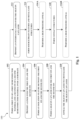
- FIG. 1 is a flow chart of a method for fabricating a semiconductor device on a workpiece, according to aspects of the present disclosure.
- FIGS. 2 - 12 are fragmentary cross-sectional views of the workpiece at various steps of the method of FIG. 1 , according to aspects of the present disclosure.
- first and second features are formed in direct contact
- additional features may be formed interposing the first and second features, such that the first and second features may not be in direct contact
- present disclosure may repeat reference numerals and/or letters in the various examples. This repetition is for the purpose of simplicity and clarity and does not in itself dictate a relationship between the various embodiments and/or configurations discussed.
- a feature on, connected to, and/or coupled to another feature in the present disclosure may include embodiments in which the features are formed in direct contact, and may also include embodiments in which additional features may be formed interposing the features, such that the features may not be in direct contact.
- spatially relative terms for example, “lower,” “upper,” “horizontal,” “vertical,” “above,” “over,” “below,” “beneath,” “up,” “down,” “top,” “bottom,” etc., as well as derivatives thereof (e.g., “horizontally,” “downwardly,” “upwardly,” etc.) are used for ease of the present disclosure of one features relationship to another feature.
- the spatially relative terms are intended to cover different orientations of the device including the features. Still further, when a number or a range of numbers is described with “about,” “approximate,” and the like, the term is intended to encompass numbers that are within a reasonable range including the number described, such as within +/ ⁇ 10% of the number described or other values as understood by person skilled in the art. For example, the term “about 5 nm” encompasses the dimension range from 4.5 nm to 5.5 nm.
- FinFET fin-shape field effect transistor
- PFETs p-type field effect transistors
- NFETs n-type field effect transistors
- electron mobility in an NFET can be enhanced with the use of fully strained silicon/carbon-doped silicon (Si/Si:C) channels, while hole mobility in PFETs can be enhanced with fully strained silicon germanium (SiGe) channels.
- Fully strained silicon/carbon-doped silicon (Si/Si:C) channels and fully strained silicon germanium (SiGe) channels may be formed using epitaxial growth.
- the fully strained epitaxial channels can be formed from epitaxial layers disposed on a top portion of a silicon (Si) fin.
- the formation process of fully strained channels requires numerous photolithography, etch, pre-treatment, anneal and growth operations.
- a silicon cap layer may be formed over workpiece to cover the fully strained p-type channel. It has been observed that properties of the silicon cap layer affect performance of the semiconductor device. When the silicon cap layer lacks crystallinity, the silicon cap layer may oxidize too quickly and may not adequately prevent germanium content in the p-type channel from oxidation.
- PFSC p-type fully strained channel
- NFSC n-type fully strained channel
- FIG. 1 illustrate a flow chart of a method 100 for fabricating a semiconductor device on a workpiece 200 .
- FIG. 1 will be described in conjunction with FIGS. 2 - 12 , which illustrate fragmentary cross-sectional views of the workpiece 200 at various stages of fabrication according to various embodiments of method 100 of the present disclosure. Additional steps can be provided before, during, and after method 100 , and some of the steps described can be moved, replaced, or eliminated for additional embodiments of method 100 . Additional features can be added in the workpiece 200 depicted in FIGS. 2 - 12 , and some of the features described below can be replaced, modified, or eliminated in other embodiments of the workpiece 200 depicted in FIGS. 2 - 12 .
- the workpiece 200 may also be referred to as the semiconductor device 200 from time to time throughout the present disclosure for convenience.
- the semiconductor device 200 can be included in a microprocessor, a memory, and/or other IC device.
- the semiconductor device 200 is a portion of an IC chip, a system on chip (SoC), or portion thereof, that includes various passive and active microelectronic devices, such as resistors, capacitors, inductors, diodes, p-type field effect transistors (PFETs), n-type field effect transistors (NFETs), metal-oxide semiconductor field effect transistors (MOSFETs), complementary metal-oxide semiconductor (CMOS) transistors, bipolar junction transistors (BJTs), laterally diffused MOS (LDMOS) transistors, high voltage transistors, high frequency transistors, other suitable components, or combinations thereof.
- various passive and active microelectronic devices such as resistors, capacitors, inductors, diodes, p-type field effect transistors (PFETs), n-type field effect transistors (NFETs), metal-oxide semiconductor field effect transistors (MOSFETs), complementary metal-oxide semiconductor (CMOS) transistors, bipolar junction transistors (BJTs), laterally diffused MOS
- the method 100 includes a block 102 where a first fin 216 A of a first semiconductor material 206 and a second fin 218 A of a second semiconductor material 204 over a substrate 202 .
- FIG. 2 illustrates the substrate 202 that includes an n-type well (n-well) 202 N and a p-type well (p-well) 202 P.
- the substrate 202 may include silicon.
- substrate 202 includes another elementary semiconductor, such as germanium; a compound semiconductor, such as silicon carbide, gallium arsenide, gallium phosphide, indium phosphide, indium arsenide, and/or indium antimonide; an alloy semiconductor, such as silicon germanium (SiGe), GaAsP, AlInAs, AlGaAs, GaInAs, GaInP, and/or GaInAsP; or combinations thereof.
- substrate 202 includes one or more group III-V materials, one or more group II-IV materials, or combinations thereof.
- substrate 202 is a semiconductor-on-insulator substrate, such as a silicon-on-insulator (SOI) substrate, a silicon germanium-on-insulator (SGOI) substrate, or a germanium-on-insulator (GOI) substrate.
- Semiconductor-on-insulator substrates can be fabricated using separation by implantation of oxygen (SIMOX), wafer bonding, and/or other suitable methods.
- SIMOX separation by implantation of oxygen
- substrate 202 consists essentially of silicon.
- the n-well 202 N include n-type dopants, such as phosphorus, arsenic, other n-type dopant, or combinations thereof.
- the p-well 202 P include p-type dopants, such as boron, indium, other p-type dopant, or combinations thereof.
- the n-well 202 N and p-well 202 P can be formed directly on and/or in substrate 202 by ion implantation processes, diffusion processes, and/or other suitable doping process.
- a layer of the first semiconductor material 206 and a layer of the second semiconductor material 204 are formed over the workpiece 200 .
- a layer of the second semiconductor material 204 is first epitaxially grown on the substrate 202 , a portion of the layer of the second semiconductor material 204 is removed to form a recess, and then a layer of the first semiconductor material 206 is epitaxially grown to fill the recess.
- the layer of the second semiconductor material 204 is not directly grown from the substrate 202 .
- a seed layer (not shown) may be formed on the substrate 202 and the layer of the second semiconductor material 204 is then formed on the seed layer.
- the second semiconductor material 204 may include silicon, carbon, or a combination thereof.
- the first semiconductor material 206 may include silicon, germanium, or a combination thereof.
- a germanium content of the first semiconductor material 206 may be between 20% and 80%.
- An example where the second semiconductor material 204 is formed of silicon is described below for illustration purposes.
- the layer of the second semiconductor material 204 is epitaxially grown to a thickness between about 50 nm to about 100 nm using source gases such as silane (SiH 4 ), silicon tetrachloride (SiCl 4 ), trichlorosilane (TCS), or dichlorosilane (SiH 2 Cl 2 or DCS).
- source gases such as silane (SiH 4 ), silicon tetrachloride (SiCl 4 ), trichlorosilane (TCS), or dichlorosilane (SiH 2 Cl 2 or DCS).
- Hydrogen (H 2 ) can be used as a reactant gas that reduces the aforementioned source gases.
- the deposition temperature during the epitaxial layer formation can range from about 700° C. to about 1250° C. depending on the gases used.
- source gases with fewer chlorine atoms may require lower formation temperatures compared to source gases with more chlorine atoms, such as SiCl 4 or TCS.
- the aforementioned ranges and type of gases are provided as examples and are not limiting.
- a hard mask formed of a dielectric material may be formed thereover.
- the hard mask may be formed of silicon oxide or silicon nitride.
- a photolithography process is then performed to pattern the hard mask.
- An etch process is then performed using the patterned hard mask as an etch mask to etch the recess in the layer of the second semiconductor material 204 .
- the etch process may be a dry etch process or a wet etch process with suitable etching chemistry.
- the etch process forming the recess does not remove all of the second semiconductor material 204 at the bottom of the recess such that a thickness of the second semiconductor material 204 at the bottom may serve as a seed layer for the first semiconductor material 206 that fills the recess.
- a layer of the first semiconductor material 206 is then formed to fill the recess in the layer of the second semiconductor material 204 .
- the layer of the first semiconductor material 206 is epitaxially grown at a temperature between about 550° C. to about 700° C. using precursor gases such as SiH 4 , Si 2 H 6 , SiH 2 Cl 2 , GeH 4 , HCl, or a combination thereof, and reactant gases such as H2, N2, or Ar, or a combination thereof.
- a planarization process such as a chemical mechanical polishing (CMP) may be performed to planarize the top surface of the first semiconductor material 206 and the second semiconductor material 204 such that they are coplanar.
- CMP chemical mechanical polishing
- the first semiconductor material 206 has a thickness between about 45 nm and about 70 nm.
- silicon top layer 208 is epitaxially grown to a thickness between about 1.5 nm and about 5 nm over the planarized top surfaces of the first semiconductor material 206 and the second semiconductor material 204 .
- the as deposited silicon top layer 208 may be trimmed by etching back or polishing to a reduced thickness between about 0.5 nm and about 4 nm.
- a hard mask 211 may be deposited over the silicon top layer 208 .
- the hard mask 211 may be a single layer or a multilayer.
- the hard mask 211 is a multilayer that includes a first hard mask layer 210 and a second hard mask layer 212 .
- the first hard mask layer 210 and the second hard mask layer 212 have different compositions.
- the first hard mask layer 210 is formed of silicon oxide and the second hard mask layer 212 is formed of silicon nitride.
- a combination of deposition, lithography and/or etching processes are performed to define the first fin 216 A and the second fin 218 A over the substrate 202 .
- forming the first fin 216 A and the second fin 218 A includes performing a lithography process to form a patterned resist layer over the hard mask 211 and performing an etching process to transfer a pattern defined in the patterned resist layer to the hard mask 211 .
- the lithography process can include forming a resist layer on the hard mask 211 , performing a pre-exposure baking process, performing an exposure process using a mask, performing a post-exposure baking process, and performing a developing process.
- the resist layer is exposed to radiation energy (such as ultraviolet (UV) light, deep UV (DUV) light, or extreme UV (EUV) light), where the mask blocks, transmits, and/or reflects radiation to the resist layer depending on a mask pattern of the mask and/or mask type (for example, binary mask, phase shift mask, or EUV mask), such that an image is projected onto the resist layer that corresponds with the mask pattern.
- radiation energy such as ultraviolet (UV) light, deep UV (DUV) light, or extreme UV (EUV) light
- EUV extreme UV
- the resist layer is sensitive to radiation energy, exposed portions of the resist layer chemically change, and exposed (or non-exposed) portions of the resist layer are dissolved during the developing process depending on characteristics of the resist layer and characteristics of a developing solution used in the developing process.
- the patterned resist layer includes a resist pattern that corresponds with the mask.
- the etching process uses the patterned resist layer as an etch mask to remove portions of the hard mask 211 .
- the etching process can include a dry etching process (for example, a reactive ion etching (RIE) process), a wet etching process, other suitable etching process, or combinations thereof.
- RIE reactive ion etching
- the patterned resist layer is removed from substrate 202 , for example, by a resist stripping process.
- first fin 216 A and the second fin 218 A are formed by a multiple patterning process, such as a double patterning lithography (DPL) process (for example, a lithography-etch-lithography-etch (LELE) process, a self-aligned double patterning (SADP) process, a spacer-is-dielectric (SID) SADP process, other double patterning process, or combinations thereof), a triple patterning process (for example, a lithography-etch-lithography-etch-lithography-etch (LELELE) process, a self-aligned triple patterning (SATP) process, other triple patterning process, or combinations thereof), other multiple patterning process (for example, self-aligned quadruple patterning (SAQP) process), or combinations thereof.
- DPL double patterning lithography
- LELE lithography-etch-lithography-etch
- SADP self-aligned double patterning
- SID spacer-is-dielectric
- a triple patterning process for example,
- DSA directed self-assembly
- the exposure process can implement maskless lithography, electron-beam (e-beam) writing, ion-beam writing, and/or nanoimprint technology for patterning the resist layer and/or other layers.
- the semiconductor device 200 includes double-fin transistors and two fins are formed over each of the n-well 202 N and the p-well 202 P.
- the first fin 216 A and an adjacent fin 216 B are formed over the n-well 202 N and the second fin 218 A and an adjacent fin 218 B are formed over the p-well 202 P.
- the first fin 216 A and the adjacent fin 216 B may be collectively referred to as p-type fins 216 and the second fin 218 A and the adjacent fin 218 B may be collectively referred to as n-type fins 218 .
- the p-type fins 216 serve as p-type active regions for formation of p-type transistors with p-type fully-strained channels.
- the n-type fins 218 serve as n-type active regions for formation of n-type transistors with n-type channels or strained n-type channels.
- the present disclosure is not to be construed restrictively. With reference to the present disclosure, a person of ordinary skill in the art would appreciate that the methods and devices disclosed in the present disclosure are readily applicable to semiconductor devices that include single-fin or multi-fin (i.e., having more than 3 fins per transistor) transistors.
- the method 100 includes a block 104 where a liner 214 is formed over the first fin 216 A and the second fin 218 A.
- the liner 214 serves to provide structural support to the first fin 216 A and the second fin 218 A during subsequent processes.
- the liner 214 may be formed of silicon nitride to a thickness between about 0.5 nm and about 3 nm.
- the liner 214 may be formed using atomic layer deposition (ALD) or chemical vapor deposition (CVD).
- the method 100 includes a block 106 where an isolation feature 220 between the first fin 216 A and the second fin 218 A.
- a dielectric material 219 is first blanketly deposited over the workpiece 200 to fill space between the p-type fins 216 and the n-type fins 218 .
- the dielectric material 219 may include silicon oxide, silicon oxynitride, other suitable isolation material, or combinations thereof and may be deposited by chemical vapor deposition (CVD) or a spin-on-glass (SOG) process.
- a planarization process such as a CMP process, is then performed until the hard mask layer 211 is removed. Referring now to FIG.
- the planarized dielectric material 219 is then etched back to form the isolation structure 220 .
- the first semiconductor material 206 and the second semiconductor material 204 in the first fin 216 A and the second semiconductor material 204 in the second fin 218 A are exposed and rise above the isolation structure 220 .
- the isolation structure 220 is a shallow trench isolation (STI) structure and may be referred to as STI structure 220 .
- STI shallow trench isolation
- the present disclosure envisions implementations of other types of isolation structure, such as deep trench isolation (DTI) structures and local oxidation of silicon (LOCOS) structures, so long as such implementation does not hinder formation of semiconductor devices with strained channels.
- DTI deep trench isolation
- LOC local oxidation of silicon
- the etching back of the dielectric material 219 also removes the liner 214 without substantially etching the isolation structure 220 , the first semiconductor material 206 and the second semiconductor material 204 .
- a separate etch process is performed to selectively remove the liner 214 .
- the separate etch process is configured to selectively etch silicon nitride.
- the method 100 includes a block 108 where a silicon cap layer 222 is formed over the first fin 216 A and the second fin 218 A,
- the silicon cap layer 222 may be deposited using suitable deposition techniques, such has atomic layer deposition (ALD) or epitaxial growth.
- the silicon cap layer 222 may be epitaxially grown to a thickness between about 0.5 nm and about 5 nm using source gases such as silane (SiH 4 ), silicon tetrachloride (SiCl 4 ), trichlorosilane (TCS), or dichlorosilane (SiH 2 Cl 2 or DCS).
- Hydrogen (H 2 ) can be used as a reactant gas that reduces the aforementioned source gases.
- the deposition temperature during the epitaxial layer formation can range from about 380° C. to about 1250° C. depending on the gases used. For example, source gases with fewer chlorine atoms (e.g., DCS) may require lower formation temperatures compared to source gases with more chlorine atoms, such as SiCl 4 or TCS.
- the silicon cap layer 222 may be formed using ALD to a similar thickness range between about 0.5 nm and about 5 nm using similar gas precursors. The difference between ALD and epitaxial grown lies primarily in that alternating self-limiting monolayers are formed in the former and the same are not necessarily formed in the latter. Other differences may include reactor types and process conditions.
- the silicon cap layer 222 is first formed to a first thickness and then recessed to a smaller second thickness that falls with the thickness range between about 0.5 nm and about 5 nm.
- the method 100 includes a block 110 where the silicon cap layer 222 undergoes an anneal process 300 to crystallize the silicon cap layer 222 .
- the anneal process 300 at block 110 is performed using radiation heating at a first temperature (T1) between about 800° C. and about 1050 C.
- T1 first temperature
- the disclosed temperature range is critical to the anneal process 300 at block 110 .
- T1 of the anneal process 300 is below 800° C., little or no reflow of silicon may take place to improve crystallinity of the silicon cap layer 222 and to reduce density of interfacial trap charge between the silicon cap layer 222 and the first semiconductor layer 206 .
- the anneal process 300 at block 110 may be performed at a first pressure (P1) between about 0.001 atmosphere (atm) and about 1.1 atm. It has been observed that a finite amount of oxygen may be needed when the anneal pressure of the anneal process 300 is well below 1 atm, such as at 0.02 atm, to control reflow of the silicon cap layer 222 .
- the finite amount of oxygen may prevent too much silicon from reflow that may result in non-uniform thickness in the silicon cap layer 222 .
- Such a finite amount of oxygen is not needed when the first pressure (P1) of the anneal process 300 is at or around 1 atm, such as at 1.02 atm.
- the anneal process 300 at block 110 may be performed in a gas ambient that includes only nitrogen, substantially free of oxygen.
- the gas ambient includes nitrogen and oxygen, with an oxygen content at between about 0.01% and about 0.05%, such as at about 0.025%.
- the gas ambient include nitrogen only. In some instances, more than one purging operation may be needed to intentionally remove oxygen gas from the gas ambient when the first pressure (P1) of the anneal process 300 is at or around 1 atm. Because the anneal process 300 is performed after formation of the silicon cap layer 222 , the anneal process 300 may be referred to as the post-silicon-cap anneal (PSA) 300 . It has been observed that PSA process 300 may effectively reduce the density of interface trap charge (DIT) at the interface between silicon cap layer 222 and the first semiconductor material 206 and to improve crystallinity of the silicon cap layer 222 .
- DIT interface trap charge
- TEM images show that a more clear-cut interface between the silicon cap layer 222 and the first semiconductor material 206 may be formed as a result of the PSA process 300 .
- the DIT is reduced because lattice defects and dislocation at the interface are reduced in the PSA at block 110 . Because the rate of oxidation of silicon decreases with crystallinity, the improved crystallinity of the silicon cap layer 222 slows down the oxidation rate and provides the first semiconductor layer 206 with better protection from undesirable oxidation.
- the relatively high first temperature T1 i.e., between about 800° C. and about 1050° C.
- the method 100 includes a block 112 where an interfacial layer 224 is deposited over the silicon cap layer 222 .
- the interfacial layer 224 includes silicon oxide and is deposited on the silicon cap layer 222 using a suitable deposition process, such as chemical vapor deposition (CVD) or atomic layer deposition (ALD).
- CVD chemical vapor deposition
- ALD atomic layer deposition
- an anneal process may be performed to anneal the deposited interfacial layer 224 to reduce imperfections and improve quality of the interfacial layer 224 .
- the method 100 includes a block 114 where source/drain features 226 , 228 and a metal gate stack 234 are formed.
- the metal gate stack 234 may be formed using a gate first process or a gate last process. The latter is described below as an example and the former is fully envisioned.
- a dummy gate stack (not shown) may be first formed over the p-type fins 216 and the n-type fins 218 such that the dummy gate stack wraps around each of the p-type fins 216 and the n-type fins 218 and engage its top surface and side surfaces.
- the dummy gate stack may include polysilicon and may be formed on the interfacial layer 224 (illustrated in FIG. 9 ).
- a gate spacer 230 may be deposited over the dummy gate stack.
- a dielectric layer (not shown) is deposited over the workpiece 200 to cover the dummy gate stack, the p-type fins 216 and the n-type fins 218 and then planarized to form a level top surface.
- photolithography processes may be then performed to sequentially expose and recess source/drain regions of the p-type fins 216 and the n-type fins 218 to form p-type source/drain features 226 and n-type source/drain feature 228 .
- Epitaxial source/drain features may then be disposed in recessed source/drain regions of the p-type fins 216 and the n-type fins 218 .
- An epitaxy process can implement CVD deposition techniques (for example, vapor-phase epitaxy (VPE), ultra-high vacuum CVD (UHV-CVD), LPCVD, and/or PECVD), molecular beam epitaxy, other suitable SEG processes, or combinations thereof.
- P-type epitaxial source/drain feature 226 may be formed of silicon germanium doped with p-type dopants, such boron.
- N-type epitaxial source/drain features 228 may be formed of silicon or Si:C doped with n-type dopants, such as phosphorus.
- annealing processes are performed to activate dopants in epitaxial source/drain features 226 and 228 of the semiconductor device 200 .
- a contact etch stop layer may be deposited over the p-type source/drain feature 226 and the n-type source/drain feature 228 .
- the CESL layer may be formed of silicon nitride or silicon carbonitride.
- an interlayer dielectric layer (ILD) 232 may be deposited over the workpiece 200 to cover the p-type source/drain features 226 and n-type source/drain feature 228 .
- the ILD 232 may be formed of silicon oxide, silicon nitride, silicon oxynitride, TEOS formed oxide, PSG, BPSG, low-k dielectric material, other suitable dielectric material, or combinations thereof.
- Exemplary low-k dielectric materials include FSG, carbon doped silicon oxide, Black Diamond® (Applied Materials of Santa Clara, Calif.), Xerogel, Aerogel, amorphous fluorinated carbon, Parylene, BCB, SiLK (Dow Chemical, Midland, Mich.), polyimide, other low-k dielectric material, or combinations thereof.
- the ILD 232 may be formed by flowable CVD (FCVD) or spin-on coating. For ease of illustration, ILD 232 is made transparent in FIG. 10 to show the gate spacer 230 .
- the ILD 232 is planarized using a suitable process such a CMP process until the dummy gate stack is exposed.
- gate replacement operations are then performed to replace the dummy gate with a metal gate stack 234 .
- the dummy gate stack and/or a portion of the interfacial layer 224 is removed to form a gate trench.
- the metal gate stack 234 is deposited in the gate trench.
- the metal gate stack 234 may include a gate dielectric layer and a gate electrode over the gate dielectric layer.
- the gate dielectric layer may include a silicon oxide layer and a high-k dielectric layer.
- the silicon oxide layer may be the leftover interfacial layer 224 or may be formed anew when all or a substantial portion of the interfacial layer 224 is removed.
- the high-k dielectric layer is formed of a dielectric material having a high dielectric constant, for example, greater than a dielectric constant of silicon oxide (k ⁇ 3.9).
- Exemplary high-k dielectric materials include hafnium, aluminum, zirconium, lanthanum, tantalum, titanium, yttrium, oxygen, nitrogen, other suitable constituent, or combinations thereof.
- the high-k dielectric layer may include, for example, HfO 2 , HfSiO, HfSiON, HfTaO, HfTiO, HfZrO, ZrO 2 , Al 2 O 3 , HfO 2 —Al 2 O 3 , TiO 2 , Ta 2 O 5 , La 2 O 3 , Y 2 O 3 , other suitable high-k dielectric material, or combinations thereof,
- the gate electrode includes an electrically conductive material.
- the gate electrode includes multiple layers, such as one or more capping layers, work function layers, glue/barrier layers, and/or metal fill (or bulk) layers.
- a capping layer can include a material that prevents or eliminates diffusion and/or reaction of constituents between the gate dielectric and other layers of the gate electrode.
- the capping layer includes a metal and nitrogen, such as titanium nitride (TiN), tantalum nitride (TaN), tungsten nitride (W 2 N), titanium silicon nitride (TiSiN), tantalum silicon nitride (TaSiN), or combinations thereof.
- a work function layer includes a conductive material tuned to have a desired work function (such as an n-type work function or a p-type work function), such as n-type work function materials and/or p-type work function materials.
- P-type work function materials include TiN, TaN, Ru, Mo, Al, WN, ZrSi 2 , MoSi 2 , TaSi 2 , NiSi 2 , WN, other p-type work function material, or combinations thereof.
- N-type work function materials include Ti, Al, Ag, Mn, Zr, TiAl, TiAlC, TaC, TaCN, TaSiN, TaAl, TaAlC, TiAlN, other n-type work function material, or combinations thereof.
- a glue/barrier layer can include a material that promotes adhesion between adjacent layers, such as the work function layer and the metal fill layer, and/or a material that blocks and/or reduces diffusion between gate layers, such as the work function layer and the metal fill layer.
- the glue/barrier layer includes metal (for example, W, Al, Ta, Ti, Ni, Cu, Co, other suitable metal, or combinations thereof), metal oxides, metal nitrides (for example, TiN), or combinations thereof.
- a metal fill layer can include a suitable conductive material, such as Al, W, and/or Cu. It is noted that the metal gate stack 234 is hidden behind the gate spacer 230 when viewed along the X direction.
- the method 100 includes a block 116 A where a high pressure anneal (HPA) process 400 is performed to the workpiece 200 .
- the HPA process 400 may be performed after formation of the source/drain features 226 , 228 and a metal gate stack 234 at block 114 .
- the method 100 may alternatively include a block 116 B (rather than block 116 A) where the HPA process 400 is performed after the block 118 (to be described below).
- IC manufacturing process flow is typically divided into three categories: front-end-of-line (FEOL), middle-end-of-line (MEOL), and back-end-of-line (BEOL).
- FEOL generally encompasses processes related to fabricating IC devices, such as transistors.
- FEOL processes can include forming active regions, isolation features, gate structures, and source/drain features.
- MEOL generally encompasses processes related to fabricating contacts to conductive features (or conductive regions) of the IC devices, such as contacts to the gate structures and/or the source/drain features.
- BEOL generally encompasses processes related to fabricating a multilayer interconnect (MLI) feature that interconnects IC features fabricated in FEOL and MEOL processes.
- MLI multilayer interconnect
- the PSA process 300 at block 110 takes place at the FEOL level or is an FEOL process; the HPA process 400 at block 116 A takes place at the MEOL level or is an MEOL process; and the HPA process 400 at block 116 B takes place at the BEOL level or is a BEOL process.
- the HPA process 400 may be performed by means of convection heating at a second temperature (T2) between about 350° C. and about 450° C., at a second pressure (P2) between about 10 atm and about 20 atm, and in a gas ambient including hydrogen.
- T2 second temperature
- P2 second pressure
- the second temperature (T2) of the HPA process 400 is smaller than the first temperature (T1) of the PSA process 300
- P2 of the HPA process 400 is greater than the first pressure (P1) of the PSA process 300 .
- the elevated second pressure (P2) is necessary to drive hydrogen from structure adjacent to channel regions into the channel regions.
- the second temperature (T2) of the HPA process 400 may not exceed 450° C. to avoid reflow or damages to metal-containing structures formed at the BEOL or the MEOL levels.
- the method 100 includes a block 118 where further processes are performed.
- further processes include formation of additional interlayer dielectric layers (ILDs) and contact features formed in the additional ILDs.
- ILDs interlayer dielectric layers
- Example of the contact features may include gate contacts to the metal gate stack (e.g., the metal gate stack 234 in FIG. 10 ), source/drain contacts 238 and 240 to the source/drain features (e.g., the p-type source/drain feature 226 and the n-type source/drain feature 228 in FIG.
- the contact feature may include a barrier layer, a liner and a metal fill layer.
- the barrier layer may be formed of Ta, TaN, TaC, Ti, TiN, TiC, and other suitable material that can block oxygen diffusion.
- the liner may be formed of suitable metal, metal nitride, or metal carbide, such as Co, CoN and RuN.
- the metal fill layer may be formed of any suitable conductive material, such as W, Ni, Ta, Ti, Al, Cu, Co, TaN, TiN, Ru, and/or other suitable conductive materials.
- the contact features are configured to route signals between devices of the semiconductor device 200 and/or distribute signals (for example, clock signals, voltage signals, and/or ground signals) to the devices of the semiconductor device 200 .
- a silicide layer 236 may be formed on the recessed p-type source/drain features 226 and n-type source/drain feature 228 .
- the silicide layer 236 is formed by depositing a metal layer over the p-type source/drain features 226 and n-type source/drain feature 228 .
- the metal layer includes any material suitable for promoting silicide formation, such as nickel, platinum, palladium, vanadium, titanium, cobalt, tantalum, ytterbium, zirconium, other suitable metal, or combinations thereof.
- the semiconductor device 200 is then heated (for example, subjected to an annealing process) to cause constituents of the p-type source/drain features 226 and n-type source/drain feature 228 (for example, silicon and/or germanium) to react with the metal.
- the silicide layers thus include metal and a constituent of the p-type source/drain features 226 and n-type source/drain feature 228 (for example, silicon and/or germanium).
- the silicide layer 236 includes nickel silicide, titanium silicide, or cobalt silicide. Any un-reacted metal, such as remaining portions of the metal layer, is selectively removed by any suitable process, such as an etching process. Operations of block 116 B in FIG. 1 are illustrated in FIG. 12 . As described above, the HPA process 400 may be performed after operations of block 118 are performed to form contact features that contain metal.
- the PSA process performed after formation of the silicon cap layer but before formation of metal gate stacks and contact features may include high anneal temperature to crystallize the silicon cap layer and to reduce DIT due to formation of the silicon cap layer, without causing reflow or damages to the metal gate stack and metal-containing contact features.
- the HPA process performed at the MEOL or the BEOL level may include high pressure to drive hydrogen into the channel regions and to reduce DIT due to processes performed after the PSA process.
- the two-stage DIT reduction disclosed in the present disclosure suppresses DIT, reduces low-field scattering, increases hole mobility, reduces sub-threshold swing, and reduces channel resistance.
- channel resistance in a p-type fully strained channel may be reduced by between about 5% and about 10%, when PSA process is performed in addition to the HPA process.
- Experimental data prove that such reduction in channel resistance is independent from channel length. In some instances, it is observed that the 5% to 10% reduction in channel resistance may approximately result in between about 5% and about 10% of increase in hole mobility.
- a method includes forming, on a substrate, a first fin formed of a first semiconductor material and a second fin formed of a second semiconductor material different from the first semiconductor material, forming a semiconductor cap layer over the first fin and the second fin, and annealing the semiconductor cap layer at a first temperature while at least a portion of the semiconductor cap layer is exposed.
- the first fin includes a p-type channel region
- the second fin includes an n-type channel region
- the first semiconductor material includes germanium
- the second semiconductor material includes silicon.
- the semiconductor cap consists essentially of silicon.
- the first temperature is greater than 800° C. In some embodiments, the first temperature is between about 800° C. and about 1050° C.
- the forming of the semiconductor cap layer includes depositing silicon using atomic layer deposition (ALD).
- the forming of the semiconductor cap layer includes epitaxially growing silicon over the first fin and the second fin. In some examples, the annealing of the semiconductor cap layer increases crystallinity of the semiconductor cap layer.
- a method in another embodiment, includes A method includes forming, on a substrate, a first fin including silicon and germanium, forming, on the substrate, a second fin including silicon, forming a silicon cap layer over the first fin and the second fin, performing a first anneal at a first temperature and a first pressure while at least a portion of the silicon cap layer is exposed, forming source/drain features over source/drain regions of the first fin and the second fin, forming a gate structure over channel regions of the first fin and the second fin, and after the forming of the gate structure, performing a second anneal at a second temperature and a second pressure while no portion of the silicon cap layer is exposed.
- the first temperature is greater than the second temperature and the second pressure is greater than the first pressure.
- a germanium content in the first fin is between about 20% and about 60%.
- the forming of the silicon cap layer includes depositing silicon using atomic layer deposition (ALD).
- the forming of the silicon cap layer includes epitaxially growing silicon over the first fin and the second fin.
- the first temperature is between about 800° C. and about 1050° C. and the first pressure is between about 0.01 atmosphere (atm) and about 1.1 atm.
- the second temperature is between about 350° C. and about 450° C. and the second pressure is between about 10 atmosphere (atm) and about 20 atm.
- the gate structure includes a high-k dielectric layer, a work function layer, and a metal fill layer.
- a method in still another embodiment, includes forming, on a substrate, a first fin including silicon and germanium, forming, on the substrate, a second fin including silicon, forming a silicon cap layer over the first fin and the second fin, and immediately after the forming of the silicon cap layer, performing a first anneal at a temperature between about 800° C. and about 1050° C.
- the forming of the silicon cap layer includes depositing silicon using atomic layer deposition (ALD). In some implementations, the forming of the silicon cap layer includes epitaxially growing silicon over the first fin and the second fin. In some instances, the method further includes forming a gate structure over channel regions of the first fin and the second fin, and after the forming of the gate structure, performing a second anneal at a temperature between about 350° C. and about 450° C.
- ALD atomic layer deposition
Landscapes
- Insulated Gate Type Field-Effect Transistor (AREA)
Abstract
Description
Claims (20)
Priority Applications (5)
| Application Number | Priority Date | Filing Date | Title |
|---|---|---|---|
| US16/926,528 US11670551B2 (en) | 2019-09-26 | 2020-07-10 | Interface trap charge density reduction |
| TW109133020A TWI752646B (en) | 2019-09-26 | 2020-09-24 | Method of fabricating semiconductor device |
| CN202011024428.1A CN112563203B (en) | 2019-09-26 | 2020-09-25 | Method for manufacturing semiconductor device |
| US18/329,396 US20230326802A1 (en) | 2019-09-26 | 2023-06-05 | Interface trap charge density reduction |
| US18/786,886 US20240387274A1 (en) | 2019-09-26 | 2024-07-29 | Interface trap charge density reduction |
Applications Claiming Priority (2)
| Application Number | Priority Date | Filing Date | Title |
|---|---|---|---|
| US201962906291P | 2019-09-26 | 2019-09-26 | |
| US16/926,528 US11670551B2 (en) | 2019-09-26 | 2020-07-10 | Interface trap charge density reduction |
Related Child Applications (1)
| Application Number | Title | Priority Date | Filing Date |
|---|---|---|---|
| US18/329,396 Continuation US20230326802A1 (en) | 2019-09-26 | 2023-06-05 | Interface trap charge density reduction |
Publications (2)
| Publication Number | Publication Date |
|---|---|
| US20210098305A1 US20210098305A1 (en) | 2021-04-01 |
| US11670551B2 true US11670551B2 (en) | 2023-06-06 |
Family
ID=75162149
Family Applications (3)
| Application Number | Title | Priority Date | Filing Date |
|---|---|---|---|
| US16/926,528 Active 2040-09-20 US11670551B2 (en) | 2019-09-26 | 2020-07-10 | Interface trap charge density reduction |
| US18/329,396 Pending US20230326802A1 (en) | 2019-09-26 | 2023-06-05 | Interface trap charge density reduction |
| US18/786,886 Pending US20240387274A1 (en) | 2019-09-26 | 2024-07-29 | Interface trap charge density reduction |
Family Applications After (2)
| Application Number | Title | Priority Date | Filing Date |
|---|---|---|---|
| US18/329,396 Pending US20230326802A1 (en) | 2019-09-26 | 2023-06-05 | Interface trap charge density reduction |
| US18/786,886 Pending US20240387274A1 (en) | 2019-09-26 | 2024-07-29 | Interface trap charge density reduction |
Country Status (2)
| Country | Link |
|---|---|
| US (3) | US11670551B2 (en) |
| TW (1) | TWI752646B (en) |
Families Citing this family (6)
| Publication number | Priority date | Publication date | Assignee | Title |
|---|---|---|---|---|
| US11670551B2 (en) * | 2019-09-26 | 2023-06-06 | Taiwan Semiconductor Manufacturing Co., Ltd. | Interface trap charge density reduction |
| CN114496741B (en) * | 2020-11-12 | 2024-10-22 | 中芯国际集成电路制造(上海)有限公司 | Method for forming semiconductor structure |
| US20230019386A1 (en) * | 2021-07-16 | 2023-01-19 | Taiwan Semiconductor Manufacturing Company, Ltd. | Isolation Features For Semiconductor Devices And Methods Of Fabricating The Same |
| US12520509B2 (en) * | 2021-12-21 | 2026-01-06 | Intel Corporation | Diode structure with backside epitaxial growth |
| US20240170581A1 (en) * | 2022-11-22 | 2024-05-23 | Intel Corporation | Backside contacted sub-fin diodes |
| US20250056865A1 (en) * | 2023-08-07 | 2025-02-13 | International Business Machines Corporation | Semiconductor device backside isolation feature integration |
Citations (51)
| Publication number | Priority date | Publication date | Assignee | Title |
|---|---|---|---|---|
| US4615766A (en) * | 1985-02-27 | 1986-10-07 | International Business Machines Corporation | Silicon cap for annealing gallium arsenide |
| US20050130358A1 (en) * | 2003-12-12 | 2005-06-16 | Dureseti Chidambarrao | Strained finFETs and method of manufacture |
| US20050255714A1 (en) * | 2002-12-20 | 2005-11-17 | Applied Materials, Inc. | Method for silicon nitride chemical vapor deposition |
| US20090090934A1 (en) * | 2007-10-05 | 2009-04-09 | Tsutomu Tezuka | Field Effect Transistor and Method for Manufacturing the Same |
| US20110006378A1 (en) * | 2009-07-07 | 2011-01-13 | Sematech, Inc. | Semiconductor Manufacturing Method Using Maskless Capping Layer Removal |
| WO2013095384A1 (en) * | 2011-12-20 | 2013-06-27 | Intel Corporation | Semiconductor device with isolated body portion |
| US8836016B2 (en) | 2012-03-08 | 2014-09-16 | Taiwan Semiconductor Manufacturing Company, Ltd. | Semiconductor structures and methods with high mobility and high energy bandgap materials |
| US8841701B2 (en) | 2011-08-30 | 2014-09-23 | Taiwan Semiconductor Manufacturing Company, Ltd. | FinFET device having a channel defined in a diamond-like shape semiconductor structure |
| US8847293B2 (en) | 2012-03-02 | 2014-09-30 | Taiwan Semiconductor Manufacturing Company, Ltd. | Gate structure for semiconductor device |
| US8853025B2 (en) | 2013-02-08 | 2014-10-07 | Taiwan Semiconductor Manufacturing Company, Ltd. | FinFET/tri-gate channel doping for multiple threshold voltage tuning |
| US20140339643A1 (en) * | 2013-05-17 | 2014-11-20 | International Busienss Machines Corporation | Finfet structures having silicon germanium and silicon fins |
| US20150021697A1 (en) * | 2013-07-17 | 2015-01-22 | Taiwan Semiconductor Manufacturing Company, Ltd. | Thermally Tuning Strain in Semiconductor Devices |
| US20150028426A1 (en) * | 2013-07-29 | 2015-01-29 | Taiwan Semiconductor Manufacturing Co., Ltd. | Buried sige oxide finfet scheme for device enhancement |
| US8962400B2 (en) | 2011-07-07 | 2015-02-24 | Taiwan Semiconductor Manufacturing Company, Ltd. | In-situ doping of arsenic for source and drain epitaxy |
| US9093514B2 (en) | 2013-03-06 | 2015-07-28 | Taiwan Semiconductor Manufacturing Co., Ltd. | Strained and uniform doping technique for FINFETs |
| TW201543667A (en) | 2014-03-27 | 2015-11-16 | Intel Corp | High mobility strain channel for fin-based NMOS transistors |
| US9190329B1 (en) * | 2014-05-20 | 2015-11-17 | International Business Machines Corporation | Complex circuits utilizing fin structures |
| US9236267B2 (en) | 2012-02-09 | 2016-01-12 | Taiwan Semiconductor Manufacturing Company, Ltd. | Cut-mask patterning process for fin-like field effect transistor (FinFET) device |
| US9245805B2 (en) | 2009-09-24 | 2016-01-26 | Taiwan Semiconductor Manufacturing Company, Ltd. | Germanium FinFETs with metal gates and stressors |
| US9373638B1 (en) * | 2015-01-15 | 2016-06-21 | International Business Machines Corporation | Complementary metal-oxide silicon having silicon and silicon germanium channels |
| US20160190168A1 (en) * | 2014-12-30 | 2016-06-30 | International Business Machines Corporation | Silicon-germanium fin formation |
| US20160190137A1 (en) * | 2014-12-26 | 2016-06-30 | Taiwan Semiconductor Manufacturing Company Ltd. | Finfet structure and method for manufacturing thereof |
| US20160190303A1 (en) * | 2014-12-31 | 2016-06-30 | Stmicroelectronics, Inc. | Silicon germanium-on-insulator finfet |
| US20160218192A1 (en) * | 2015-01-28 | 2016-07-28 | International Business Machines Corporation | Integration of strained silicon germanium pfet device and silicon nfet device for finfet structures |
| US20160268378A1 (en) * | 2015-03-12 | 2016-09-15 | Globalfoundries Inc. | Integrated strained fin and relaxed fin |
| US9461174B2 (en) * | 2014-08-01 | 2016-10-04 | Stmicroelectronics, Inc. | Method for the formation of silicon and silicon-germanium fin structures for FinFET devices |
| US20160307807A1 (en) * | 2015-04-20 | 2016-10-20 | Globalfoundries Inc. | Punch-through-stop after partial fin etch |
| US9484266B1 (en) * | 2015-08-04 | 2016-11-01 | International Business Machines Corporation | Complementary heterogeneous MOSFET using global SiGe substrate and hard-mask memorized germanium dilution for nFET |
| US9520482B1 (en) | 2015-11-13 | 2016-12-13 | Taiwan Semiconductor Manufacturing Company, Ltd. | Method of cutting metal gate |
| US20160372551A1 (en) * | 2015-06-19 | 2016-12-22 | International Business Machines Corporation | Silicon germanium fin formation via condensation |
| US20170005190A1 (en) * | 2015-06-30 | 2017-01-05 | International Business Machines Corporation | Local germanium condensation for suspended nanowire and finfet devices |
| US9548386B1 (en) * | 2015-08-31 | 2017-01-17 | International Business Machines Corporation | Structure and method for compressively strained silicon germanium fins for pFET devices and tensily strained silicon fins for nFET devices |
| US9576814B2 (en) | 2013-12-19 | 2017-02-21 | Taiwan Semiconductor Manufacturing Company, Ltd. | Method of spacer patterning to form a target integrated circuit pattern |
| US20170069543A1 (en) * | 2015-09-03 | 2017-03-09 | United Microelectronics Corp. | Method for fabricating semiconductor device |
| US9847334B1 (en) * | 2016-11-18 | 2017-12-19 | Taiwan Semiconductor Manufacturing Co., Ltd. | Structure and formation method of semiconductor device with channel layer |
| US20180090494A1 (en) * | 2016-09-28 | 2018-03-29 | International Business Machines Corporation | Semiconductor device and method of forming the semiconductor device |
| US20180315663A1 (en) * | 2017-04-26 | 2018-11-01 | International Business Machines Corporation | Dual channel silicon/silicon germanium complementary metal oxide semiconductor performance with interface engineering |
| US20180337097A1 (en) * | 2017-05-16 | 2018-11-22 | International Business Machines Corporation | Dual channel cmos having common gate stacks |
| US20180337101A1 (en) * | 2017-05-19 | 2018-11-22 | Semiconductor Manufacturing International (Shanghai) Corporation | Semiconductor structures and fabrication methods thereof |
| TW201913756A (en) | 2017-08-31 | 2019-04-01 | 台灣積體電路製造股份有限公司 | Methods of forming semiconductor devices, fin field-effect transistor devices and methods of forming the same |
| US20190148141A1 (en) * | 2015-09-30 | 2019-05-16 | Taiwan Semiconductor Manufacturiing Company Limited | Semiconductor device and method for forming the same |
| US20190245049A1 (en) * | 2018-02-07 | 2019-08-08 | International Business Machines Corporation | Self-limiting fin spike removal |
| US20190295844A1 (en) * | 2018-03-23 | 2019-09-26 | International Business Machines Corporation | Gate Stack Designs for Analog and Logic Devices in Dual Channel Si/SiGe CMOS |
| US20200006533A1 (en) * | 2018-06-29 | 2020-01-02 | Taiwan Semiconductor Manufacturing Company, Ltd. | Semiconductor Device and Method |
| US20200091319A1 (en) * | 2018-09-18 | 2020-03-19 | International Business Machines Corporation | Oxide isolated fin-type field-effect transistors |
| US20200135584A1 (en) * | 2018-10-28 | 2020-04-30 | Taiwan Semiconductor Manufacturing Co., Ltd. | Finfet devices and methods of forming the same |
| US20200168507A1 (en) * | 2018-11-28 | 2020-05-28 | Taiwan Semiconductor Manufacturing Company Ltd. | Semiconductor structure and method of forming the same |
| US10699967B2 (en) * | 2018-06-28 | 2020-06-30 | International Business Machines Corporation | Co-integration of high carrier mobility PFET and NFET devices on the same substrate using low temperature condensation |
| US20210066476A1 (en) * | 2019-08-30 | 2021-03-04 | Taiwan Semiconductor Manufacturing Co., Ltd. | Semiconductor Device Structure With Uniform Threshold Voltage Distribution And Method Of Forming The Same |
| US20210098305A1 (en) * | 2019-09-26 | 2021-04-01 | Taiwan Semiconductor Manufacturing Co., Ltd. | Interface Trap Charge Density Reduction |
| US20210296506A1 (en) * | 2020-03-20 | 2021-09-23 | Intel Corporation | Fabrication of non-planar silicon germanium transistors using silicon replacement |
Family Cites Families (19)
| Publication number | Priority date | Publication date | Assignee | Title |
|---|---|---|---|---|
| US8815742B2 (en) * | 2012-12-12 | 2014-08-26 | Globalfoundries Inc. | Methods of forming bulk FinFET semiconductor devices by performing a liner recessing process to define fin heights and FinFET devices with such a recessed liner |
| US8835262B2 (en) * | 2013-01-08 | 2014-09-16 | Globalfoundries Inc. | Methods of forming bulk FinFET devices by performing a recessing process on liner materials to define different fin heights and FinFET devices with such recessed liner materials |
| US8895446B2 (en) * | 2013-02-18 | 2014-11-25 | Taiwan Semiconductor Manufacturing Company, Ltd. | Fin deformation modulation |
| US9824410B1 (en) * | 2013-04-29 | 2017-11-21 | Grubhub Holdings Inc. | System, method and apparatus for assessing the accuracy of estimated food delivery time |
| US20140374838A1 (en) * | 2013-06-21 | 2014-12-25 | Taiwan Semiconductor Manufacturing Company, Ltd. | FinFETs with Nitride Liners and Methods of Forming the Same |
| US9142474B2 (en) * | 2013-10-07 | 2015-09-22 | Taiwan Semiconductor Manufacturing Company, Ltd. | Passivation structure of fin field effect transistor |
| US9287262B2 (en) * | 2013-10-10 | 2016-03-15 | Taiwan Semiconductor Manufacturing Company, Ltd. | Passivated and faceted for fin field effect transistor |
| US9419134B2 (en) * | 2014-01-13 | 2016-08-16 | Taiwan Semiconductor Manufacturing Company, Ltd. | Strain enhancement for FinFETs |
| US9219116B2 (en) * | 2014-01-15 | 2015-12-22 | Taiwan Semiconductor Manufacturing Company, Ltd. | Fin structure of semiconductor device |
| US9362404B2 (en) * | 2014-02-21 | 2016-06-07 | Taiwan Semiconductor Manufacturing Company, Ltd. | Doping for FinFET |
| US9443769B2 (en) * | 2014-04-21 | 2016-09-13 | Taiwan Semiconductor Manufacturing Company, Ltd. | Wrap-around contact |
| US9276117B1 (en) * | 2014-08-19 | 2016-03-01 | Taiwan Semiconductor Manufacturing Company, Ltd. | Structure and method and FinFET device |
| KR102320820B1 (en) * | 2015-02-24 | 2021-11-02 | 삼성전자주식회사 | Integrated circuit device and method of manufacturing the same |
| US9947675B1 (en) * | 2016-09-29 | 2018-04-17 | International Business Machines Corporation | Mask-programmable ROM using a vertical FET integration process |
| US10515952B2 (en) * | 2017-08-04 | 2019-12-24 | Taiwan Semiconductor Manufacturing Co., Ltd. | Fin field effect transistor (FinFET) device structure and method for forming the same |
| US10680106B2 (en) * | 2017-11-15 | 2020-06-09 | Taiwan Semiconductor Manufacturing Co., Ltd. | Method of forming source/drain epitaxial stacks |
| US11296077B2 (en) * | 2018-11-19 | 2022-04-05 | Taiwan Semiconductor Manufacturing Company, Ltd. | Transistors with recessed silicon cap and method forming same |
| US11264274B2 (en) * | 2019-09-27 | 2022-03-01 | Tokyo Electron Limited | Reverse contact and silicide process for three-dimensional logic devices |
| US11133230B2 (en) * | 2020-02-26 | 2021-09-28 | Taiwan Semiconductor Manufacturing Co., Ltd. | Semiconductor device with dual isolation liner and method of forming the same |
-
2020
- 2020-07-10 US US16/926,528 patent/US11670551B2/en active Active
- 2020-09-24 TW TW109133020A patent/TWI752646B/en active
-
2023
- 2023-06-05 US US18/329,396 patent/US20230326802A1/en active Pending
-
2024
- 2024-07-29 US US18/786,886 patent/US20240387274A1/en active Pending
Patent Citations (64)
| Publication number | Priority date | Publication date | Assignee | Title |
|---|---|---|---|---|
| US4615766A (en) * | 1985-02-27 | 1986-10-07 | International Business Machines Corporation | Silicon cap for annealing gallium arsenide |
| US20050255714A1 (en) * | 2002-12-20 | 2005-11-17 | Applied Materials, Inc. | Method for silicon nitride chemical vapor deposition |
| US20050130358A1 (en) * | 2003-12-12 | 2005-06-16 | Dureseti Chidambarrao | Strained finFETs and method of manufacture |
| US20090090934A1 (en) * | 2007-10-05 | 2009-04-09 | Tsutomu Tezuka | Field Effect Transistor and Method for Manufacturing the Same |
| US20110006378A1 (en) * | 2009-07-07 | 2011-01-13 | Sematech, Inc. | Semiconductor Manufacturing Method Using Maskless Capping Layer Removal |
| US9245805B2 (en) | 2009-09-24 | 2016-01-26 | Taiwan Semiconductor Manufacturing Company, Ltd. | Germanium FinFETs with metal gates and stressors |
| US8962400B2 (en) | 2011-07-07 | 2015-02-24 | Taiwan Semiconductor Manufacturing Company, Ltd. | In-situ doping of arsenic for source and drain epitaxy |
| US8841701B2 (en) | 2011-08-30 | 2014-09-23 | Taiwan Semiconductor Manufacturing Company, Ltd. | FinFET device having a channel defined in a diamond-like shape semiconductor structure |
| WO2013095384A1 (en) * | 2011-12-20 | 2013-06-27 | Intel Corporation | Semiconductor device with isolated body portion |
| US9236267B2 (en) | 2012-02-09 | 2016-01-12 | Taiwan Semiconductor Manufacturing Company, Ltd. | Cut-mask patterning process for fin-like field effect transistor (FinFET) device |
| US8847293B2 (en) | 2012-03-02 | 2014-09-30 | Taiwan Semiconductor Manufacturing Company, Ltd. | Gate structure for semiconductor device |
| US8836016B2 (en) | 2012-03-08 | 2014-09-16 | Taiwan Semiconductor Manufacturing Company, Ltd. | Semiconductor structures and methods with high mobility and high energy bandgap materials |
| US8853025B2 (en) | 2013-02-08 | 2014-10-07 | Taiwan Semiconductor Manufacturing Company, Ltd. | FinFET/tri-gate channel doping for multiple threshold voltage tuning |
| US9093514B2 (en) | 2013-03-06 | 2015-07-28 | Taiwan Semiconductor Manufacturing Co., Ltd. | Strained and uniform doping technique for FINFETs |
| US20140339643A1 (en) * | 2013-05-17 | 2014-11-20 | International Busienss Machines Corporation | Finfet structures having silicon germanium and silicon fins |
| US20150206744A1 (en) * | 2013-05-17 | 2015-07-23 | International Business Machines Corporation | Finfet structures having silicon germanium and silicon fins |
| US20150206904A1 (en) * | 2013-05-17 | 2015-07-23 | International Business Machines Corporation | Finfet structures having silicon germanium and silicon fins |
| US20150021697A1 (en) * | 2013-07-17 | 2015-01-22 | Taiwan Semiconductor Manufacturing Company, Ltd. | Thermally Tuning Strain in Semiconductor Devices |
| US20150028426A1 (en) * | 2013-07-29 | 2015-01-29 | Taiwan Semiconductor Manufacturing Co., Ltd. | Buried sige oxide finfet scheme for device enhancement |
| US9202917B2 (en) * | 2013-07-29 | 2015-12-01 | Taiwan Semiconductor Manufacturing Co., Ltd. | Buried SiGe oxide FinFET scheme for device enhancement |
| US9576814B2 (en) | 2013-12-19 | 2017-02-21 | Taiwan Semiconductor Manufacturing Company, Ltd. | Method of spacer patterning to form a target integrated circuit pattern |
| TW201543667A (en) | 2014-03-27 | 2015-11-16 | Intel Corp | High mobility strain channel for fin-based NMOS transistors |
| US9190329B1 (en) * | 2014-05-20 | 2015-11-17 | International Business Machines Corporation | Complex circuits utilizing fin structures |
| US9461174B2 (en) * | 2014-08-01 | 2016-10-04 | Stmicroelectronics, Inc. | Method for the formation of silicon and silicon-germanium fin structures for FinFET devices |
| US20160190137A1 (en) * | 2014-12-26 | 2016-06-30 | Taiwan Semiconductor Manufacturing Company Ltd. | Finfet structure and method for manufacturing thereof |
| US20170077269A1 (en) * | 2014-12-26 | 2017-03-16 | Taiwan Semiconductor Manufacturing Company Ltd. | Finfet structure and method for manufacturing thereof |
| US20160190168A1 (en) * | 2014-12-30 | 2016-06-30 | International Business Machines Corporation | Silicon-germanium fin formation |
| US20160190303A1 (en) * | 2014-12-31 | 2016-06-30 | Stmicroelectronics, Inc. | Silicon germanium-on-insulator finfet |
| US9373638B1 (en) * | 2015-01-15 | 2016-06-21 | International Business Machines Corporation | Complementary metal-oxide silicon having silicon and silicon germanium channels |
| US20160218192A1 (en) * | 2015-01-28 | 2016-07-28 | International Business Machines Corporation | Integration of strained silicon germanium pfet device and silicon nfet device for finfet structures |
| US20160268378A1 (en) * | 2015-03-12 | 2016-09-15 | Globalfoundries Inc. | Integrated strained fin and relaxed fin |
| US20160307807A1 (en) * | 2015-04-20 | 2016-10-20 | Globalfoundries Inc. | Punch-through-stop after partial fin etch |
| US20160372551A1 (en) * | 2015-06-19 | 2016-12-22 | International Business Machines Corporation | Silicon germanium fin formation via condensation |
| US20170005190A1 (en) * | 2015-06-30 | 2017-01-05 | International Business Machines Corporation | Local germanium condensation for suspended nanowire and finfet devices |
| US9484266B1 (en) * | 2015-08-04 | 2016-11-01 | International Business Machines Corporation | Complementary heterogeneous MOSFET using global SiGe substrate and hard-mask memorized germanium dilution for nFET |
| US9548386B1 (en) * | 2015-08-31 | 2017-01-17 | International Business Machines Corporation | Structure and method for compressively strained silicon germanium fins for pFET devices and tensily strained silicon fins for nFET devices |
| US20170069543A1 (en) * | 2015-09-03 | 2017-03-09 | United Microelectronics Corp. | Method for fabricating semiconductor device |
| US20190148141A1 (en) * | 2015-09-30 | 2019-05-16 | Taiwan Semiconductor Manufacturiing Company Limited | Semiconductor device and method for forming the same |
| US9520482B1 (en) | 2015-11-13 | 2016-12-13 | Taiwan Semiconductor Manufacturing Company, Ltd. | Method of cutting metal gate |
| US20180090494A1 (en) * | 2016-09-28 | 2018-03-29 | International Business Machines Corporation | Semiconductor device and method of forming the semiconductor device |
| US9847334B1 (en) * | 2016-11-18 | 2017-12-19 | Taiwan Semiconductor Manufacturing Co., Ltd. | Structure and formation method of semiconductor device with channel layer |
| US20180315663A1 (en) * | 2017-04-26 | 2018-11-01 | International Business Machines Corporation | Dual channel silicon/silicon germanium complementary metal oxide semiconductor performance with interface engineering |
| US20190229020A1 (en) | 2017-04-26 | 2019-07-25 | International Business Machines Corporation | Dual channel silicon/silicon germanium complementary metal oxide semiconductor performance with interface engineering |
| US20180337098A1 (en) * | 2017-05-16 | 2018-11-22 | International Business Machines Corporation | Dual channel cmos having common gate stacks |
| US20180337097A1 (en) * | 2017-05-16 | 2018-11-22 | International Business Machines Corporation | Dual channel cmos having common gate stacks |
| US20180337101A1 (en) * | 2017-05-19 | 2018-11-22 | Semiconductor Manufacturing International (Shanghai) Corporation | Semiconductor structures and fabrication methods thereof |
| TW201913756A (en) | 2017-08-31 | 2019-04-01 | 台灣積體電路製造股份有限公司 | Methods of forming semiconductor devices, fin field-effect transistor devices and methods of forming the same |
| US20190245049A1 (en) * | 2018-02-07 | 2019-08-08 | International Business Machines Corporation | Self-limiting fin spike removal |
| US20190295844A1 (en) * | 2018-03-23 | 2019-09-26 | International Business Machines Corporation | Gate Stack Designs for Analog and Logic Devices in Dual Channel Si/SiGe CMOS |
| US20200144057A1 (en) * | 2018-03-23 | 2020-05-07 | International Business Machines Corporation | Gate Stack Designs for Analog and Logic Devices in Dual Channel Si/SiGe CMOS |
| US10699967B2 (en) * | 2018-06-28 | 2020-06-30 | International Business Machines Corporation | Co-integration of high carrier mobility PFET and NFET devices on the same substrate using low temperature condensation |
| US10923403B2 (en) * | 2018-06-28 | 2021-02-16 | International Business Machines Corporation | Co-integration of high carrier mobility PFET and NFET devices on the same substrate using low temperature condensation |
| US20200006533A1 (en) * | 2018-06-29 | 2020-01-02 | Taiwan Semiconductor Manufacturing Company, Ltd. | Semiconductor Device and Method |
| US10680083B2 (en) * | 2018-09-18 | 2020-06-09 | International Business Machines Corporation | Oxide isolated fin-type field-effect transistors |
| US20200243670A1 (en) * | 2018-09-18 | 2020-07-30 | International Business Machines Corporation | Oxide isolated fin-type field-effect transistors |
| US20200091319A1 (en) * | 2018-09-18 | 2020-03-19 | International Business Machines Corporation | Oxide isolated fin-type field-effect transistors |
| US11094801B2 (en) * | 2018-09-18 | 2021-08-17 | International Business Machines Corporation | Oxide isolated fin-type field-effect transistors |
| US20200135584A1 (en) * | 2018-10-28 | 2020-04-30 | Taiwan Semiconductor Manufacturing Co., Ltd. | Finfet devices and methods of forming the same |
| US20210104441A1 (en) * | 2018-10-28 | 2021-04-08 | Taiwan Semiconductor Manufacturing Company, Ltd. | Finfet devices and methods of forming the same |
| US20200168507A1 (en) * | 2018-11-28 | 2020-05-28 | Taiwan Semiconductor Manufacturing Company Ltd. | Semiconductor structure and method of forming the same |
| US11031291B2 (en) * | 2018-11-28 | 2021-06-08 | Taiwan Semiconductor Manufacturing Company Ltd. | Semiconductor structure and method of forming the same |
| US20210066476A1 (en) * | 2019-08-30 | 2021-03-04 | Taiwan Semiconductor Manufacturing Co., Ltd. | Semiconductor Device Structure With Uniform Threshold Voltage Distribution And Method Of Forming The Same |
| US20210098305A1 (en) * | 2019-09-26 | 2021-04-01 | Taiwan Semiconductor Manufacturing Co., Ltd. | Interface Trap Charge Density Reduction |
| US20210296506A1 (en) * | 2020-03-20 | 2021-09-23 | Intel Corporation | Fabrication of non-planar silicon germanium transistors using silicon replacement |
Non-Patent Citations (1)
| Title |
|---|
| Sprenger et al., "Electron-enhanced atomic layer deposition of silicon thin films at room temperature", J. Vac. Sci. Technol. A (36)1, Jan./Feb. 2018, pp. 01A118-1 tp 01A118-10 . . . (Year: 2018). * |
Also Published As
| Publication number | Publication date |
|---|---|
| TW202121538A (en) | 2021-06-01 |
| US20230326802A1 (en) | 2023-10-12 |
| TWI752646B (en) | 2022-01-11 |
| US20210098305A1 (en) | 2021-04-01 |
| US20240387274A1 (en) | 2024-11-21 |
Similar Documents
| Publication | Publication Date | Title |
|---|---|---|
| US12376367B2 (en) | Threshold voltage tuning for fin-based integrated circuit device | |
| US12538518B2 (en) | FinFET structure with fin top hard mask and method of forming the same | |
| CN109817580B (en) | Integrated circuit device and method of manufacturing an integrated circuit device | |
| US20240387274A1 (en) | Interface trap charge density reduction | |
| US11145650B2 (en) | Gate cut dielectric feature and method of forming the same | |
| US12283630B2 (en) | Epitaxial source/drain structures for multigate devices and methods of fabricating thereof | |
| US12336281B2 (en) | Gate structures having neutral zones to minimize metal gate boundary effects and methods of fabricating thereof | |
| US12302611B2 (en) | FinFET structure with a composite stress layer and reduced fin buckling | |
| US20250280572A1 (en) | Multigate device with stressor layers and method of fabricating thereof | |
| US10971402B2 (en) | Semiconductor device including interface layer and method of fabricating thereof | |
| CN112563203B (en) | Method for manufacturing semiconductor device | |
| US20240047561A1 (en) | Semiconductor device and method for forming the same | |
| US20240055480A1 (en) | Semiconductor structure and manufacturing method thereof |
Legal Events
| Date | Code | Title | Description |
|---|---|---|---|
| AS | Assignment |
Owner name: TAIWAN SEMICONDUCTOR MANUFACTURING CO., LTD., TAIWAN Free format text: ASSIGNMENT OF ASSIGNORS INTEREST;ASSIGNORS:YANG, SZU-CHI;CHIEN, ALLEN;DING, CHENG-TING;AND OTHERS;SIGNING DATES FROM 20200306 TO 20200310;REEL/FRAME:053179/0759 |
|
| FEPP | Fee payment procedure |
Free format text: ENTITY STATUS SET TO UNDISCOUNTED (ORIGINAL EVENT CODE: BIG.); ENTITY STATUS OF PATENT OWNER: LARGE ENTITY |
|
| STPP | Information on status: patent application and granting procedure in general |
Free format text: DOCKETED NEW CASE - READY FOR EXAMINATION |
|
| STPP | Information on status: patent application and granting procedure in general |
Free format text: NON FINAL ACTION MAILED |
|
| STPP | Information on status: patent application and granting procedure in general |
Free format text: RESPONSE TO NON-FINAL OFFICE ACTION ENTERED AND FORWARDED TO EXAMINER |
|
| STPP | Information on status: patent application and granting procedure in general |
Free format text: FINAL REJECTION MAILED |
|
| STPP | Information on status: patent application and granting procedure in general |
Free format text: ADVISORY ACTION MAILED |
|
| STPP | Information on status: patent application and granting procedure in general |
Free format text: DOCKETED NEW CASE - READY FOR EXAMINATION |
|
| STCF | Information on status: patent grant |
Free format text: PATENTED CASE |