US11653563B2 - Organic light-emitting device - Google Patents
Organic light-emitting device Download PDFInfo
- Publication number
- US11653563B2 US11653563B2 US15/374,170 US201615374170A US11653563B2 US 11653563 B2 US11653563 B2 US 11653563B2 US 201615374170 A US201615374170 A US 201615374170A US 11653563 B2 US11653563 B2 US 11653563B2
- Authority
- US
- United States
- Prior art keywords
- group
- substituted
- unsubstituted
- salt
- aromatic condensed
- Prior art date
- Legal status (The legal status is an assumption and is not a legal conclusion. Google has not performed a legal analysis and makes no representation as to the accuracy of the status listed.)
- Active, expires
Links
Images


Classifications
-
- H01L51/0067—
-
- C—CHEMISTRY; METALLURGY
- C09—DYES; PAINTS; POLISHES; NATURAL RESINS; ADHESIVES; COMPOSITIONS NOT OTHERWISE PROVIDED FOR; APPLICATIONS OF MATERIALS NOT OTHERWISE PROVIDED FOR
- C09K—MATERIALS FOR MISCELLANEOUS APPLICATIONS, NOT PROVIDED FOR ELSEWHERE
- C09K11/00—Luminescent materials, e.g. electroluminescent or chemiluminescent
- C09K11/02—Use of particular materials as binders, particle coatings or suspension media therefor
- C09K11/025—Use of particular materials as binders, particle coatings or suspension media therefor non-luminescent particle coatings or suspension media
-
- C—CHEMISTRY; METALLURGY
- C09—DYES; PAINTS; POLISHES; NATURAL RESINS; ADHESIVES; COMPOSITIONS NOT OTHERWISE PROVIDED FOR; APPLICATIONS OF MATERIALS NOT OTHERWISE PROVIDED FOR
- C09K—MATERIALS FOR MISCELLANEOUS APPLICATIONS, NOT PROVIDED FOR ELSEWHERE
- C09K11/00—Luminescent materials, e.g. electroluminescent or chemiluminescent
- C09K11/06—Luminescent materials, e.g. electroluminescent or chemiluminescent containing organic luminescent materials
-
- H01L51/0061—
-
- H01L51/0071—
-
- H01L51/0085—
-
- H—ELECTRICITY
- H10—SEMICONDUCTOR DEVICES; ELECTRIC SOLID-STATE DEVICES NOT OTHERWISE PROVIDED FOR
- H10K—ORGANIC ELECTRIC SOLID-STATE DEVICES
- H10K50/00—Organic light-emitting devices
- H10K50/10—OLEDs or polymer light-emitting diodes [PLED]
- H10K50/11—OLEDs or polymer light-emitting diodes [PLED] characterised by the electroluminescent [EL] layers
- H10K50/12—OLEDs or polymer light-emitting diodes [PLED] characterised by the electroluminescent [EL] layers comprising dopants
-
- H—ELECTRICITY
- H10—SEMICONDUCTOR DEVICES; ELECTRIC SOLID-STATE DEVICES NOT OTHERWISE PROVIDED FOR
- H10K—ORGANIC ELECTRIC SOLID-STATE DEVICES
- H10K85/00—Organic materials used in the body or electrodes of devices covered by this subclass
- H10K85/30—Coordination compounds
- H10K85/341—Transition metal complexes, e.g. Ru(II)polypyridine complexes
- H10K85/342—Transition metal complexes, e.g. Ru(II)polypyridine complexes comprising iridium
-
- H—ELECTRICITY
- H10—SEMICONDUCTOR DEVICES; ELECTRIC SOLID-STATE DEVICES NOT OTHERWISE PROVIDED FOR
- H10K—ORGANIC ELECTRIC SOLID-STATE DEVICES
- H10K85/00—Organic materials used in the body or electrodes of devices covered by this subclass
- H10K85/60—Organic compounds having low molecular weight
- H10K85/631—Amine compounds having at least two aryl rest on at least one amine-nitrogen atom, e.g. triphenylamine
- H10K85/636—Amine compounds having at least two aryl rest on at least one amine-nitrogen atom, e.g. triphenylamine comprising heteroaromatic hydrocarbons as substituents on the nitrogen atom
-
- H—ELECTRICITY
- H10—SEMICONDUCTOR DEVICES; ELECTRIC SOLID-STATE DEVICES NOT OTHERWISE PROVIDED FOR
- H10K—ORGANIC ELECTRIC SOLID-STATE DEVICES
- H10K85/00—Organic materials used in the body or electrodes of devices covered by this subclass
- H10K85/60—Organic compounds having low molecular weight
- H10K85/649—Aromatic compounds comprising a hetero atom
- H10K85/654—Aromatic compounds comprising a hetero atom comprising only nitrogen as heteroatom
-
- H—ELECTRICITY
- H10—SEMICONDUCTOR DEVICES; ELECTRIC SOLID-STATE DEVICES NOT OTHERWISE PROVIDED FOR
- H10K—ORGANIC ELECTRIC SOLID-STATE DEVICES
- H10K85/00—Organic materials used in the body or electrodes of devices covered by this subclass
- H10K85/60—Organic compounds having low molecular weight
- H10K85/649—Aromatic compounds comprising a hetero atom
- H10K85/657—Polycyclic condensed heteroaromatic hydrocarbons
- H10K85/6572—Polycyclic condensed heteroaromatic hydrocarbons comprising only nitrogen in the heteroaromatic polycondensed ring system, e.g. phenanthroline or carbazole
-
- C—CHEMISTRY; METALLURGY
- C09—DYES; PAINTS; POLISHES; NATURAL RESINS; ADHESIVES; COMPOSITIONS NOT OTHERWISE PROVIDED FOR; APPLICATIONS OF MATERIALS NOT OTHERWISE PROVIDED FOR
- C09K—MATERIALS FOR MISCELLANEOUS APPLICATIONS, NOT PROVIDED FOR ELSEWHERE
- C09K2211/00—Chemical nature of organic luminescent or tenebrescent compounds
- C09K2211/10—Non-macromolecular compounds
- C09K2211/1003—Carbocyclic compounds
- C09K2211/1007—Non-condensed systems
-
- C—CHEMISTRY; METALLURGY
- C09—DYES; PAINTS; POLISHES; NATURAL RESINS; ADHESIVES; COMPOSITIONS NOT OTHERWISE PROVIDED FOR; APPLICATIONS OF MATERIALS NOT OTHERWISE PROVIDED FOR
- C09K—MATERIALS FOR MISCELLANEOUS APPLICATIONS, NOT PROVIDED FOR ELSEWHERE
- C09K2211/00—Chemical nature of organic luminescent or tenebrescent compounds
- C09K2211/10—Non-macromolecular compounds
- C09K2211/1018—Heterocyclic compounds
- C09K2211/1022—Heterocyclic compounds bridged by heteroatoms, e.g. N, P, Si or B
-
- C—CHEMISTRY; METALLURGY
- C09—DYES; PAINTS; POLISHES; NATURAL RESINS; ADHESIVES; COMPOSITIONS NOT OTHERWISE PROVIDED FOR; APPLICATIONS OF MATERIALS NOT OTHERWISE PROVIDED FOR
- C09K—MATERIALS FOR MISCELLANEOUS APPLICATIONS, NOT PROVIDED FOR ELSEWHERE
- C09K2211/00—Chemical nature of organic luminescent or tenebrescent compounds
- C09K2211/10—Non-macromolecular compounds
- C09K2211/1018—Heterocyclic compounds
- C09K2211/1025—Heterocyclic compounds characterised by ligands
- C09K2211/1029—Heterocyclic compounds characterised by ligands containing one nitrogen atom as the heteroatom
- C09K2211/1037—Heterocyclic compounds characterised by ligands containing one nitrogen atom as the heteroatom with sulfur
-
- C—CHEMISTRY; METALLURGY
- C09—DYES; PAINTS; POLISHES; NATURAL RESINS; ADHESIVES; COMPOSITIONS NOT OTHERWISE PROVIDED FOR; APPLICATIONS OF MATERIALS NOT OTHERWISE PROVIDED FOR
- C09K—MATERIALS FOR MISCELLANEOUS APPLICATIONS, NOT PROVIDED FOR ELSEWHERE
- C09K2211/00—Chemical nature of organic luminescent or tenebrescent compounds
- C09K2211/10—Non-macromolecular compounds
- C09K2211/1018—Heterocyclic compounds
- C09K2211/1025—Heterocyclic compounds characterised by ligands
- C09K2211/1044—Heterocyclic compounds characterised by ligands containing two nitrogen atoms as heteroatoms
- C09K2211/1051—Heterocyclic compounds characterised by ligands containing two nitrogen atoms as heteroatoms with sulfur
-
- C—CHEMISTRY; METALLURGY
- C09—DYES; PAINTS; POLISHES; NATURAL RESINS; ADHESIVES; COMPOSITIONS NOT OTHERWISE PROVIDED FOR; APPLICATIONS OF MATERIALS NOT OTHERWISE PROVIDED FOR
- C09K—MATERIALS FOR MISCELLANEOUS APPLICATIONS, NOT PROVIDED FOR ELSEWHERE
- C09K2211/00—Chemical nature of organic luminescent or tenebrescent compounds
- C09K2211/10—Non-macromolecular compounds
- C09K2211/1018—Heterocyclic compounds
- C09K2211/1025—Heterocyclic compounds characterised by ligands
- C09K2211/1059—Heterocyclic compounds characterised by ligands containing three nitrogen atoms as heteroatoms
- C09K2211/1066—Heterocyclic compounds characterised by ligands containing three nitrogen atoms as heteroatoms with sulfur
-
- C—CHEMISTRY; METALLURGY
- C09—DYES; PAINTS; POLISHES; NATURAL RESINS; ADHESIVES; COMPOSITIONS NOT OTHERWISE PROVIDED FOR; APPLICATIONS OF MATERIALS NOT OTHERWISE PROVIDED FOR
- C09K—MATERIALS FOR MISCELLANEOUS APPLICATIONS, NOT PROVIDED FOR ELSEWHERE
- C09K2211/00—Chemical nature of organic luminescent or tenebrescent compounds
- C09K2211/10—Non-macromolecular compounds
- C09K2211/1018—Heterocyclic compounds
- C09K2211/1025—Heterocyclic compounds characterised by ligands
- C09K2211/1074—Heterocyclic compounds characterised by ligands containing more than three nitrogen atoms as heteroatoms
- C09K2211/1081—Heterocyclic compounds characterised by ligands containing more than three nitrogen atoms as heteroatoms with sulfur
-
- C—CHEMISTRY; METALLURGY
- C09—DYES; PAINTS; POLISHES; NATURAL RESINS; ADHESIVES; COMPOSITIONS NOT OTHERWISE PROVIDED FOR; APPLICATIONS OF MATERIALS NOT OTHERWISE PROVIDED FOR
- C09K—MATERIALS FOR MISCELLANEOUS APPLICATIONS, NOT PROVIDED FOR ELSEWHERE
- C09K2211/00—Chemical nature of organic luminescent or tenebrescent compounds
- C09K2211/18—Metal complexes
- C09K2211/185—Metal complexes of the platinum group, i.e. Os, Ir, Pt, Ru, Rh or Pd
-
- H01L51/0072—
-
- H01L51/5012—
-
- H01L51/5056—
-
- H01L51/5072—
-
- H01L51/5088—
-
- H01L51/5092—
-
- H01L51/5096—
-
- H01L51/5206—
-
- H01L51/5221—
-
- H—ELECTRICITY
- H10—SEMICONDUCTOR DEVICES; ELECTRIC SOLID-STATE DEVICES NOT OTHERWISE PROVIDED FOR
- H10K—ORGANIC ELECTRIC SOLID-STATE DEVICES
- H10K2101/00—Properties of the organic materials covered by group H10K85/00
- H10K2101/10—Triplet emission
-
- H—ELECTRICITY
- H10—SEMICONDUCTOR DEVICES; ELECTRIC SOLID-STATE DEVICES NOT OTHERWISE PROVIDED FOR
- H10K—ORGANIC ELECTRIC SOLID-STATE DEVICES
- H10K50/00—Organic light-emitting devices
- H10K50/10—OLEDs or polymer light-emitting diodes [PLED]
- H10K50/11—OLEDs or polymer light-emitting diodes [PLED] characterised by the electroluminescent [EL] layers
-
- H—ELECTRICITY
- H10—SEMICONDUCTOR DEVICES; ELECTRIC SOLID-STATE DEVICES NOT OTHERWISE PROVIDED FOR
- H10K—ORGANIC ELECTRIC SOLID-STATE DEVICES
- H10K50/00—Organic light-emitting devices
- H10K50/10—OLEDs or polymer light-emitting diodes [PLED]
- H10K50/14—Carrier transporting layers
- H10K50/15—Hole transporting layers
-
- H—ELECTRICITY
- H10—SEMICONDUCTOR DEVICES; ELECTRIC SOLID-STATE DEVICES NOT OTHERWISE PROVIDED FOR
- H10K—ORGANIC ELECTRIC SOLID-STATE DEVICES
- H10K50/00—Organic light-emitting devices
- H10K50/10—OLEDs or polymer light-emitting diodes [PLED]
- H10K50/14—Carrier transporting layers
- H10K50/16—Electron transporting layers
-
- H—ELECTRICITY
- H10—SEMICONDUCTOR DEVICES; ELECTRIC SOLID-STATE DEVICES NOT OTHERWISE PROVIDED FOR
- H10K—ORGANIC ELECTRIC SOLID-STATE DEVICES
- H10K50/00—Organic light-emitting devices
- H10K50/10—OLEDs or polymer light-emitting diodes [PLED]
- H10K50/17—Carrier injection layers
-
- H—ELECTRICITY
- H10—SEMICONDUCTOR DEVICES; ELECTRIC SOLID-STATE DEVICES NOT OTHERWISE PROVIDED FOR
- H10K—ORGANIC ELECTRIC SOLID-STATE DEVICES
- H10K50/00—Organic light-emitting devices
- H10K50/10—OLEDs or polymer light-emitting diodes [PLED]
- H10K50/17—Carrier injection layers
- H10K50/171—Electron injection layers
-
- H—ELECTRICITY
- H10—SEMICONDUCTOR DEVICES; ELECTRIC SOLID-STATE DEVICES NOT OTHERWISE PROVIDED FOR
- H10K—ORGANIC ELECTRIC SOLID-STATE DEVICES
- H10K50/00—Organic light-emitting devices
- H10K50/10—OLEDs or polymer light-emitting diodes [PLED]
- H10K50/18—Carrier blocking layers
-
- H—ELECTRICITY
- H10—SEMICONDUCTOR DEVICES; ELECTRIC SOLID-STATE DEVICES NOT OTHERWISE PROVIDED FOR
- H10K—ORGANIC ELECTRIC SOLID-STATE DEVICES
- H10K50/00—Organic light-emitting devices
- H10K50/80—Constructional details
- H10K50/805—Electrodes
- H10K50/81—Anodes
-
- H—ELECTRICITY
- H10—SEMICONDUCTOR DEVICES; ELECTRIC SOLID-STATE DEVICES NOT OTHERWISE PROVIDED FOR
- H10K—ORGANIC ELECTRIC SOLID-STATE DEVICES
- H10K50/00—Organic light-emitting devices
- H10K50/80—Constructional details
- H10K50/805—Electrodes
- H10K50/82—Cathodes
-
- H—ELECTRICITY
- H10—SEMICONDUCTOR DEVICES; ELECTRIC SOLID-STATE DEVICES NOT OTHERWISE PROVIDED FOR
- H10K—ORGANIC ELECTRIC SOLID-STATE DEVICES
- H10K85/00—Organic materials used in the body or electrodes of devices covered by this subclass
- H10K85/60—Organic compounds having low molecular weight
- H10K85/615—Polycyclic condensed aromatic hydrocarbons, e.g. anthracene
- H10K85/626—Polycyclic condensed aromatic hydrocarbons, e.g. anthracene containing more than one polycyclic condensed aromatic rings, e.g. bis-anthracene
Definitions
- Exemplary embodiments of the present invention relate to a light-emitting device, and more particularly to an organic light-emitting device.
- OLEDs Organic light-emitting devices
- OLEDs may be self-emission devices.
- OLEDs may have relatively wide viewing angles, relatively high contrast ratios, and relatively short response times.
- OLEDs may produce full-color images.
- OLEDs may also have an increased brightness, driving voltage, and response speed characteristics.
- OLEDs may include a first electrode disposed on a substrate.
- OLEDs may include a hole transport region, an emission layer, an electron transport region, and a second electrode sequentially disposed on the first electrode. Holes provided from the first electrode may move toward the emission layer through the hole transport region. Electrons provided from the second electrode may move toward the emission layer through the electron transport region. Carriers, such as holes and electrons, may recombine in the emission layer to produce excitons. The excitons may transition from an excited state to a ground state, thus generating light.
- One or more exemplary embodiments of the present invention include an organic light-emitting device having relatively low driving voltage and relatively high efficiency.
- an organic light-emitting device includes:
- an organic layer disposed between the first electrode and the second electrode, the organic layer including an emission layer, a first compound, and a second compound.
- the first compound is represented by Formula 1.
- the second compound is represented by one of Formulae 2A and 2B.
- ring A 2 , ring A 3 , and ring A 4 are condensed with each other; and ring A 12 , ring A 13 , and ring A 14 are condensed with each other;
- ring A 1 , ring A 2 , ring A 4 , ring A 11 , ring A 12 , ring A 14 , and ring A 21 to ring A 24 are each independently selected from a C 5 -C 30 carbocyclic group and a C 2 -C 30 heterocyclic group;
- ring A 3 is a group represented by Formula 10-1, and ring A 13 is a group represented by Formula 10-2;
- X 1 is selected from N-(L 5 ) a5 -(Ar 2 ) b2 , oxygen (O), and sulfur (S);
- X 11 is selected from N-(L 12 ) a12 -(Ar 12 ) b12 , O, and S;
- L 1 to L 5 , L 11 , L 12 , L 21 , and L 31 are each independently selected from a substituted or unsubstituted C 3 -C 10 cycloalkylene group, a substituted or unsubstituted C 1 -C 10 heterocycloalkylene group, a substituted or unsubstituted C 3 -C 10 cycloalkenylene group, a substituted or unsubstituted C 1 -C 10 heterocycloalkenylene group, a substituted or unsubstituted C 6 -C 60 arylene group, a substituted or unsubstituted C 1 -C 60 heteroarylene group, a substituted or unsubstituted divalent non-aromatic condensed polycyclic group, and a substituted or unsubstituted divalent non-aromatic condensed heteropolycyclic group;
- a1 to a5, a11, a12, a21, and a31 are each independently an integer selected from 0 to 3;
- Ar 1 , Ar 2 , Ar 11 , Ar 12 , Ar 21 , Ar 22 , Ar 31 , and Ar 32 are each independently selected from a group represented by Formula 1-1, a substituted or unsubstituted C 3 -C 10 cycloalkyl group, a substituted or unsubstituted C 1 -C 10 heterocycloalkyl group, a substituted or unsubstituted C 3 -C 10 cycloalkenyl group, a substituted or unsubstituted C 1 -C 10 heterocycloalkenyl group, a substituted or unsubstituted C 6 -C 60 aryl group, a substituted or unsubstituted C 1 -C 60 heteroaryl group, a substituted or unsubstituted monovalent non-aromatic condensed polycyclic group, and a substituted or unsubstituted monovalent non-aromatic condensed heteropolycyclic group;
- b1, b2, b11, and b12 are each independently an integer selected from 1 to 5,
- Ar 31 and Ar 32 are connected to each other to form a saturated ring or an unsaturated ring;
- R 1 to R 6 , R 11 to R 13 , and R 21 to R 24 are each independently selected from a group represented by Formula 1-2, a group represented by Formula 20, hydrogen, deuterium, —F, —Cl, —Br, —I, a hydroxyl group, a cyano group, a nitro group, an amino group, an amidino group, a hydrazine group, a hydrazone group, a carboxylic acid group or a salt thereof, a sulfonic acid group or a salt thereof, a phosphoric acid group or a salt thereof, a substituted or unsubstituted C 1 -C 60 alkyl group, a substituted or unsubstituted C 2 -C 60 alkenyl group, a substituted or unsubstituted C 2 -C 60 alkynyl group, a substituted or unsubstituted C 1 -C 60 alkoxy group, a substituted or unsubstitute
- c1 to c6, c11 to c13, and c21 to c24 are each independently an integer selected from 0 to 4;
- n1 to n3 are each independently an integer selected from 0 to 4;
- R 21 and R 22 is be a group represented by Formula 20, and at least one of R 23 and R 24 is a group represented by Formula 20;
- * indicates a binding site to a neighboring atom
- the substituted C 3 -C 10 cycloalkylene group the substituted C 1 -C 10 heterocycloalkylene group, the substituted C 3 -C 10 cycloalkenylene group, the substituted C 1 -C 10 heterocycloalkenylene group, the substituted C 6 -C 60 arylene group, the substituted C 1 -C 60 heteroarylene group, the substituted divalent non-aromatic condensed polycyclic group, the substituted divalent non-aromatic condensed heteropolycyclic group, the substituted C 1 -C 60 alkyl group, the substituted C 2 -C 60 alkenyl group, the substituted C 2 -C 60 alkynyl group, the substituted C 1 -C 60 alkoxy group, the substituted C 3 -C 10 cycloalkyl group, the substituted C 1 -C 10 heterocycloalkyl group, the substituted C 3 -C 10 cycloalkenyl group, the
- deuterium —F, —Cl, —Br, —I, a hydroxyl group, a cyano group, a nitro group, an amino group, an amidino group, a hydrazine group, a hydrazone group, a carboxylic acid group or a salt thereof, a sulfonic acid group or a salt thereof, a phosphoric acid group or a salt thereof, a C 1 -C 60 alkyl group, a C 2 -C 60 alkenyl group, a C 2 -C 60 alkynyl group, and a C 1 -C 60 alkoxy group;
- Q 1 to Q 3 , Q 11 to Q 15 , Q 21 to Q 25 , and Q 31 to Q 35 are each independently selected from hydrogen, deuterium, —F, —Cl, —Br, —I, a hydroxyl group, a cyano group, a nitro group, an amino group, an amidino group, a hydrazine group, a hydrazone group, a carboxylic acid group or a salt thereof, a sulfonic acid group or a salt thereof, a phosphoric acid group or a salt thereof, a C 1 -C 60 alkyl group, a C 2 -C 60 alkenyl group, a C 2 -C 60 alkynyl group, a C 1 -C 60 alkoxy group, a C 3 -C 10 cycloalkyl group, a C 1 -C 10 heterocycloalkyl group, a C 3 -C 10 cycloalkenyl group, a C 1 -
- FIG. 1 is a schematic cross-sectional diagram illustrating an organic light-emitting device according to an exemplary embodiment of the present invention.
- a component such as a layer, a film, a region, or a plate
- the component can be directly on the other component or intervening components may be present.
- an organic light-emitting device may include a first electrode, a second electrode facing the first electrode, and an organic layer.
- the organic layer may include an emission layer.
- the organic layer may be disposed between the first electrode and the second electrode.
- the organic layer may include a first compound and a second compound.
- the first electrode may be an anode.
- the second electrode may be a cathode.
- the first electrode and the second electrode may each independently be as defined herein.
- the first compound may be represented by Formulae 1
- the second compound may be represented by one of Formulae 2A and 2B:
- ring A 2 , ring A 3 , and ring A 4 may be chemically bonded to each other, and ring A 12 , ring A 13 , and ring A 14 may be chemically bonded to each other.
- ring A 1 , ring A 2 , ring A 4 , ring A 11 , ring A 12 , ring A 14 , and ring A 21 to ring A 24 may each independently be selected from a C 5 -C 30 carbocyclic group and a C 2 -C 30 heterocyclic group.
- ring A 1 , ring A 2 , ring A 4 , ring A 11 , ring A 12 , ring A 14 , and ring A 21 to ring A 24 in Formulae 1, 1-1, 1-2, 2A, and 2B may each independently be selected from a benzene group, a naphthalene group, a pyridine group, a pyrimidine group, a quinoline group, an isoquinoline group, a benzoquinoline group, a quinoxaline group, a quinazoline group, and a phenanthroline group.
- ring A 1 , ring A 4 , ring A 11 , ring A 14 , and ring A 21 to ring A 24 may each independently be selected from a benzene group and a naphthalene group, and ring A 2 and ring A 12 may each independently be a naphthalene group; however, exemplary embodiments of the present invention are not limited thereto.
- ring A 3 may be a group represented by Formula 10-1
- ring A 13 may be a group represented by Formula 10-2:
- X 1 may be selected from N-(L 5 ) a5 -(Ar 2 ) b2 , oxygen (O), and sulfur (S), and X 11 may be selected from N-(L 12 ) a12 -(Ar 12 ) b12 , O, and S.
- L 5 , L 12 , a5, a12, Ar 2 , Ar 12 , b2, and b12 may each independently be as defined herein.
- X 1 and X 11 may each independently be selected from O and S. According to an exemplary embodiment of the present invention, X 1 and X 11 may each independently be 5, however, exemplary embodiments of the present invention are not limited thereto.
- L 1 to L 5 , L 11 , L 12 , L 21 , and L 31 may each independently be selected from a substituted or unsubstituted C 3 -C 10 cycloalkylene group, a substituted or unsubstituted C 1 -C 10 heterocycloalkylene group, a substituted or unsubstituted C 3 -C 10 cycloalkenylene group, a substituted or unsubstituted C 1 -C 10 heterocycloalkenylene group, a substituted or unsubstituted C 6 -C 60 arylene group, a substituted or unsubstituted C 1 -C 60 heteroarylene group, a substituted or unsubstituted divalent non-aromatic condensed polycyclic group, and a substituted or unsubstituted divalent non-aromatic condensed heteropolycyclic group.
- L 1 to L 5 , L 11 , L 12 , L 21 , and L 31 may each independently be selected from:
- L 1 to L 5 , L 11 , L 12 , L 21 , and L 31 may each independently be selected from groups represented by Formulae 3-1 to 3-41:
- Y 1 may be selected from O, S, C(Z 3 )(Z 4 ), N(Z 5 ), and Si(Z 6 )(Z 7 );
- Z 1 to Z 7 may each independently be selected from hydrogen, deuterium, —F, —Cl, —Br, —I, a hydroxyl group, a cyano group, a nitro group, an amino group, an amidino group, a hydrazine group, a hydrazone group, a carboxylic acid group or a salt thereof, a sulfonic acid group or a salt thereof, a phosphoric acid group or a salt thereof, a C 1 -C 20 alkyl group, a C 1 -C 20 alkoxy group, a phenyl group, a biphenyl group, a terphenyl group, a naphthyl group, a fluorenyl group, a spiro-fluorenyl group, a benzofluorenyl group, a dibenzofluorenyl group, a phenanthrenyl group, an anthracenyl group, a pyreny
- Q 33 to Q 35 may each independently be selected from a C 1 -C 10 alkyl group, a C 1 -C 10 alkoxy group, a phenyl group, a biphenyl group, a terphenyl group, and a naphthyl group;
- d2 may be an integer selected from 1 and 2;
- d3 may be an integer selected from 1 to 3;
- d4 may be an integer selected from 1 to 4.
- d5 may be an integer selected from 1 to 5;
- d6 may be an integer selected from 1 to 6;
- d8 may be an integer selected from 1 to 8.
- * and *′ may each independently indicate a binding site to a neighboring atom.
- L 1 to L 5 , L 11 , L 12 , L 21 , and L 31 may each independently be selected from groups represented by Formulae 4-1 to 4-37:
- * and *′ may each independently indicate a binding site to a neighboring atom.
- a1 to a5, a11, a12, a21, and a31 may each independently be an integer selected from 0 to 3.
- a1 may indicate the number of L 1 (s) in Formula 1.
- a1 is 2 or greater, at least two L 1 (s) may be the same as or different from each other.
- *-(L 1 ) a1 -*′ may be a single bond.
- a2 to a5, a11, a12, a21, and a31 may each independently be the same as described herein with reference to with a1 and Formulae 1, 1-2, 2A, 2B, 10-1, 10-2, and 20.
- a1 and a2 may each independently be an integer selected from 0, 1, and 2.
- a3 to a5, a11, a1, and a31 may each independently be an integer selected from 0 and 1.
- a21 may be an integer selected from 1 and 2.
- exemplary embodiments of the present invention are not limited thereto.
- Ar 1 , Ar 2 , Ar 11 , Ar 12 , Ar 21 , Ar 22 , Ar 31 , and Ar 32 may each independently be selected from a group represented by Formula 1-1, a substituted or unsubstituted C 3 -C 10 cycloalkyl group, a substituted or unsubstituted C 1 -C 10 heterocycloalkyl group, a substituted or unsubstituted C 3 -C 10 cycloalkenyl group, a substituted or unsubstituted C 1 -C 10 heterocycloalkenyl group, a substituted or unsubstituted C 6 -C 60 aryl group, a substituted or unsubstituted C 1 -C 60 heteroaryl group, a substituted or unsubstituted monovalent non-aromatic condensed polycyclic group, and a substituted or unsubstituted monovalent non-aromatic condensed polycyclic group, and a substituted or unsubsti
- Ar 1 , Ar 2 , Ar 11 , Ar 12 , Ar 21 , Ar 22 , Ar 31 , and Ar 32 may each independently be selected from a group represented by Formula 1-1, a phenyl group, a biphenyl group, a terphenyl group, a pentalenyl group, an indenyl group, a naphthyl group, an azulenyl group, a heptalenyl group, an indacenyl group, an acenaphthyl group, a fluorenyl group, a spiro-fluorenyl group, a benzofluorenyl group, a dibenzofluorenyl group, a phenalenyl group, a phenanthrenyl group, an anthracenyl group, a fluoranthenyl group, a triphenylenyl group, a pyrenyl group, a chryseny
- a phenyl group a biphenyl group, a terphenyl group, a pentalenyl group, an indenyl group, a naphthyl group, an azulenyl group, a heptalenyl group, an indacenyl group, an acenaphthyl group, a fluorenyl group, a spiro-fluorenyl group, a benzofluorenyl group, a dibenzofluorenyl group, a phenalenyl group, a phenanthrenyl group, an anthracenyl group, a fluoranthenyl group, a triphenylenyl group, a pyrenyl group, a chrysenyl group, a naphthacenyl group, a picenyl group, a perylenyl group, a pentaphenyl group, a hexacenyl
- Q 31 to Q 33 may each independently be selected from hydrogen, deuterium, —F, —Cl, —Br, —I, a hydroxyl group, a cyano group, a nitro group, an amino group, an amidino group, a hydrazine group, a hydrazone group, a carboxylic acid group or a salt thereof, a sulfonic acid group or a salt thereof, a phosphoric acid group or a salt thereof, a C 1 -C 20 alkyl group, a C 1 -C 20 alkoxy group, a phenyl group, a biphenyl group, a terphenyl group, a naphthyl group, a fluorenyl group, a spiro-fluorenyl group, a benzofluorenyl group, a dibenzofluorenyl group, a phenanthrenyl group, an anthracenyl group, a pyreny
- Ar 1 , Ar 2 , Ar 11 , Ar 12 , Ar 21 , Ar 22 , Ar 31 , and Ar 32 may each independently be selected from groups represented by Formulae 1-1 and 5-1 to 5-79:
- Y 11 may be selected from O, S, C(Z 13 )(Z 14 ), N(Z 15 ), and Si(Z 16 )(Z 17 );
- Z 11 to Z 17 may each independently be selected from hydrogen, deuterium, —F, —Cl, —Br, —I, a hydroxyl group, a cyano group, a nitro group, an amino group, an amidino group, a hydrazine group, a hydrazone group, a carboxylic acid group or a salt thereof, a sulfonic acid group or a salt thereof, a phosphoric acid group or a salt thereof, a C 1 -C 20 alkyl group, a C 1 -C 20 alkoxy group, a phenyl group, a biphenyl group, a terphenyl group, a naphthyl group, a fluorenyl group, a spiro-fluorenyl group, a benzofluorenyl group, a dibenzofluorenyl group, a phenanthrenyl group, an anthracenyl group, a pyreny
- Q 33 to Q 35 may each independently be selected from a C 1 -C 10 alkyl group, a alkoxy group, a phenyl group, a biphenyl group, a terphenyl group, and a naphthyl group;
- e2 may be an integer selected from 1 and 2;
- e3 may be an integer selected from 1 to 3;
- e4 may be an integer selected from 1 to 4;
- e5 may be an integer selected from 1 to 5;
- e6 may be an integer selected from 1 to 6;
- e8 may be an integer selected from 1 to 8.
- * may indicate a binding site to a neighboring atom.
- Ar t , Ar 2 , Ar 11 , Ar 12 , Ar 21 , Ar 22 , Ar 31 , and Ar 32 in Formulae 1, 1-2, 2A, 10-1, 10-2, and 20 may each independently be selected from groups represented by Formulae 1-1 and 6-1 to 6-158:
- * may indicate a binding site to a neighboring atom.
- Ar 1 may be selected from groups represented by Formulae 1-1 and 5-1 to 5-79, e.g., groups represented by Formulae 6-1 to 6-158
- Ar 2 , Ar 11 , Ar 12 , Ar 21 , Ar 22 , Ar 31 , and Ar 32 may each independently be selected from groups represented by Formulae 5-1 to 5-79, e.g., groups represented by Formulae 6-1 to 6-158.
- Ar 31 and Ar 32 may be connected to each other and may form a saturated or unsaturated ring.
- b1, b2, b11, and b12 may each independently be an integer selected from 1 to 5.
- b1 may indicate the number of Ar 1 (s) in Formula 1.
- b1 is 2 or greater, at least two Ar 1 (s) may be the same or different from each other.
- b2, b11, and b12 may each independently be the same as described herein with reference to b1 and Formulae 1-2, 10-1, and 10-2.
- b1, b2, b11, and b12 may each independently be an integer selected from 1 and 2; however, exemplary embodiments of the present invention are not limited thereto.
- R 1 to R 6 , R 11 to R 13 and R 21 to R 24 may each independently be selected from a group represented by Formula 1-2, a group represented by Formula 20, hydrogen, deuterium, —F, —Cl, —Br, —I, a hydroxyl group, a cyano group, a nitro group, an amino group, an amidino group, a hydrazine group, a hydrazone group, a carboxylic acid group or a salt thereof, a sulfonic acid group or a salt thereof, a phosphoric acid group or a salt thereof, a substituted or unsubstituted C 1 -C 60 alkyl group, a substituted or unsubstituted C 2 -C 60 alkenyl group, a substituted or unsubstituted C 2 -C 60 alkynyl group, a substituted or unsubstituted C 1 -C 60
- R 1 to R 6 , R 11 to R 13 , and R 21 to R 24 in Formulae 1, 1-1, 1-2, 2A, and 2B may each independently be selected from a group represented by Formula 1-2, a group represented by Formula 20, hydrogen, deuterium, —F, —Cl, —Br, —I, a hydroxyl group, a cyano group, a nitro group, an amino group, an amidino group, a hydrazine group, a hydrazone group, a carboxylic acid group or a salt thereof, a sulfonic acid group or a salt thereof, a phosphoric acid group or a salt thereof, a substituted or unsubstituted C 1 -C 20 alkyl group, a substituted or unsubstituted C 1 -C 20 alkoxy group, a substituted or unsubstituted C 6 -C 20 aryl group, a substituted or unsubstituted C 1 -
- R 1 to R 6 , R 11 to R 13 , and R 21 to R 24 in Formulae 1, 1-1, 1-2, 2A, and 2B may each independently be selected from:
- a group represented by Formula 1-2 a group represented by Formula 20, hydrogen, deuterium, —F, —Cl, —Br, —I, a hydroxyl group, a cyano group, a nitro group, an amino group, an amidino group, a hydrazine group, a hydrazone group, a carboxylic acid group or a salt thereof, a sulfonic acid group or a salt thereof, a phosphoric acid group or a salt thereof, a C 1 -C 20 alkyl group, and a C 1 -C 20 alkoxy group;
- a C 1 -C 20 alkyl group and a C 1 -C 20 alkoxy group each substituted with at least one selected from deuterium, —F, —Cl, —Br, —I, a hydroxyl group, a cyano group, a nitro group, an amino group, an amidino group, a hydrazine group, a hydrazone group, a carboxylic acid group or a salt thereof, a sulfonic acid group or a salt thereof, or a phosphoric acid group and a salt thereof;
- a phenyl group a biphenyl group, a terphenyl group, a pentalenyl group, an indenyl group, a naphthyl group, an azulenyl group, a heptalenyl group, an indacenyl group, an acenaphthyl group, a fluorenyl group, a spiro-fluorenyl group, a benzofluorenyl group, a dibenzofluorenyl group, a phenalenyl group, a phenanthrenyl group, an anthracenyl group, a fluoranthenyl group, a triphenylenyl group (triphenylenyl), a pyrenyl group, a chrysenyl group, a naphthacenyl group, a picenyl group, a perylenyl group, a pentaphenyl group,
- a phenyl group a biphenyl group, a terphenyl group, a pentalenyl group, an indenyl group, a naphthyl group, an azulenyl group, a heptalenyl group, an indacenyl group, an acenaphthyl group, a fluorenyl group, a spiro-fluorenyl group, a benzofluorenyl group, a dibenzofluorenyl group, a phenalenyl group, a phenanthrenyl group, an anthracenyl group, a fluoranthenyl group, a triphenylenyl group, a pyrenyl group, a chrysenyl group, a naphthacenyl group, a picenyl group, a perylenyl group, a pentaphenyl group, a hexacenyl
- Q 3 to Q 5 and Q 33 to Q 35 may each independently be selected from a C 1 -C 10 alkyl group, a C 1 -C 10 alkoxy group, a phenyl group, a biphenyl group, a terphenyl group, and a naphthyl group.
- R 1 to R 6 in Formula 1 may each independently be selected from a group represented by Formula 1-2, a group represented by Formula 20, hydrogen, deuterium, —F, —Cl, —Br, —I, a hydroxyl group, a cyano group, a nitro group, a carboxylic acid group or a salt thereof, a sulfonic acid group or a salt thereof, a phosphoric acid group or a salt thereof, a C 1 -C 10 alkyl group, and a C 1 -C 10 alkoxy group,
- R 11 to R 13 in Formulae 1-1 and 1-2 may each independently be selected from:
- a phenyl group a biphenyl group, a terphenyl group, a naphthyl group, a pyridinyl group, a pyrimidinyl group, and a triazinyl group;
- a phenyl group, a naphthyl group, a pyridinyl group, a pyrimidinyl group, and a triazinyl group each substituted with at least one selected from deuterium, —F, —Cl, —Br, —I, a hydroxyl group, a cyano group, a nitro group, an amino group, an amidino group, a hydrazine group, a hydrazone group, a carboxylic acid group or a salt thereof, a sulfonic acid group or a salt thereof, a phosphoric acid group or a salt thereof, a C 1 -C 10 alkyl group, a C 1 -C 10 alkoxy group, a phenyl group, a biphenyl group, a terphenyl group, a naphthyl group, a pyridinyl group, a pyrimidinyl group, a triazinyl group,
- Q 1 to Q 3 and Q 31 to Q 33 may each independently be selected from a C 1 -C 10 alkyl group, a C 1 -C 10 alkoxy group, a phenyl group, a biphenyl group, a terphenyl group, and a naphthyl group; and
- R 21 to R 24 in Formulae 2A and 2B may each independently be selected from a group represented by Formula 20, hydrogen, deuterium, —F, —Cl, —Br, —I, a hydroxyl group, a cyano group, a nitro group, a carboxylic acid group or a salt thereof, a sulfonic acid group or a salt thereof, a phosphoric acid group or a salt thereof, a C 1 -C 10 alkyl group, and a C 1 -C 10 alkoxy group.
- R 1 in Formula 1 may be selected from hydrogen and groups represented by Formulae 1-2 and 20;
- R 1 to R 6 and R 11 to R 13 in Formulae 1, 1-1, and 1-2 may each independently be hydrogen;
- R 21 to R 24 in Formulae 2A and 2B may each independently be selected from hydrogen and a group represented by Formula 20. At least one of R 21 and R 22 may be a group represented by Formula 20. At least one of R 23 and R 24 may be a group represented by Formula 20.
- c1 to c6, c11 to c13, and c21 to c24 may each independently be an integer selected from 0 to 4.
- c1 may indicate the number of R 1 (s) in Formula 1.
- c2 to c6, c11 to c13, and c21 to c24 may each independently be the same as c1 and as described herein with reference to Formulae 1, 1-1, 1-2, 2A, and 2B.
- c1 to c6, c11 to c13, and c21 to c24 in Formulae 1, 1-1, 1-2, 2A, and 2B may each independently be an integer selected from 0 and 1.
- n1 to n3 may each independently be an integer selected from 0 to 4.
- n1 may indicate the number of *-(L 2 ) a2 -(R 1 ) c1 (s).
- n2 and n3 may each independently be the same as n1 as described herein with reference to Formula 1.
- n1 to n3 may each independently be an integer selected from 0 and 1.
- the first compound may be represented by one selected from Formulae 1A to 1L
- the second compound may be represented by one selected from Formulae 2A-1 and 2B-1:
- ring A 1 , ring A 4 , ring A 11 , ring A 14 , X 1 , X 11 , L 1 , L 2 , L 11 , L 21 , a1, a2, a11, a21, Ar 1 , Ar 11 , Ar 21 , Ar 22 , b1, b11, R 1 to R 6 , R 11 to R 13 , R 21 to R 24 , C1 to c6, c11 to c13, and c21 to c24 may each independently be as defined herein.
- the first compound may be represented by one selected from Formulae 1A-1, 1A-2, 1B-1, and 1C-1
- the second compound may be represented by one selected from Formulae 2A-1(1) and 2B-1(1):
- X 1 , X 11 , L 1 , L 2 , L 11 , L 21 , L 31 , a1, a2, a11, a31, Ar 1 , Ar 11 , Ar 21 , Ar 22 , Ar 31 , Ar 32 , b1, and b11 may each independently be as defined herein;
- Ar 31a and Ar 31b may each independently be the same as Ar 31 as described herein;
- Ar 32a and Ar 32b may each independently be the same as Ar 32 as described herein.
- X 1 and X 11 may each independently be O or S;
- L 1 , L 2 , L 11 , L 21 , and L 31 may each independently be selected from groups represented by Formulae 4-1 to 4-37;
- a1 may be an integer selected from 0, 1, and 2;
- a2, a11, and a31 may each independently be an integer selected from 0 and 1;
- Ar 1 , Ar 11 , Ar 21 , Ar 22 , Ar 31 , Ar 31a , Ar 31b , Ar 32 , Ar 32a , and Ar 32b may each independently be selected from groups represented by Formulae 6-1 to 6-158.
- the first compound may be one selected from Compounds 1-1 to 1-72:
- the second compound may be one selected from Compounds 2-1 to 2-51:
- the first electrode may be an anode.
- the second electrode may be a cathode.
- the organic layer may include a hole transport region and an electron transport region.
- the hole transport region may be disposed between the first electrode and the emission layer.
- the hole transport region may include at least one selected from a hole injection layer, a hole transport layer, a buffer layer, and an electron blocking layer.
- the electron transport region may be disposed between the emission layer and the second electrode.
- the electron transport region may include at least one selected from a hole blocking layer, an electron transport layer, and an electron injection layer.
- the first electrode in the organic light-emitting device, may be an anode.
- the second electrode may be a cathode.
- the emission layer may include the first compound.
- the hole transport region may include the second compound.
- the first compound may include at least two five-membered heterorings. Due to the inclusion of the two or more five-membered heterorings, the first compound may provide a relatively high glass transition temperature (Tg) or a relatively high melting point. Thus, the first compound may contribute to a relatively high heat resistance to Joule heating, which may occur during electroluminescent emission. The first compound may contribute to a relatively high reliability under high-temperature environments. Thus, the organic light-emitting device including the first compound may exhibit a relatively high durability during high-temperature storage and driving.
- Tg glass transition temperature
- Joule heating which may occur during electroluminescent emission.
- the first compound may contribute to a relatively high reliability under high-temperature environments.
- the organic light-emitting device including the first compound may exhibit a relatively high durability during high-temperature storage and driving.
- the organic light-emitting device including the first compound and the second compound may achieve a relatively low driving voltage and a relatively high efficiency. Additionally, the inclusion of the first compound in the organic light-emitting device may lead to increased emission efficiency. The inclusion of the second compound in the organic light-emitting device may lead to a decrease or prevention of exciton leakage. Thus, the organic light-emitting device including the first compound and the second compound may have a relatively reduced power consumption, which may lead to an increased emission efficiency.
- FIG. 1 is a schematic cross-sectional diagram of an organic light-emitting device according to an exemplary embodiment of the present invention.
- an organic light-emitting device 10 may include a first electrode 110 , a hole transport region 130 , an emission layer 150 , an electron transport region 170 , and a second electrode 190 .
- the first electrode 110 , the hole transport region 130 , the emission layer 150 , the electron transport region 170 , and the second electrode may be sequentially stacked.
- the substrate may be disposed under the first electrode 110 .
- the substrate may be disposed above the second electrode 190 .
- the substrate may include a glass substrate or a plastic substrate.
- the glass substrate and the plastic substrate may each have a relatively high mechanical strength, thermal stability, transparency, surface smoothness, ease of handling, and water resistance.
- the first electrode 110 may be formed by, for example, depositing or sputtering a material for forming the first electrode 110 on the substrate.
- the material for forming the first electrode 110 may include materials with a relatively high work function, which may facilitate hole injection.
- the first electrode 110 may be a reflective electrode, a semi-transmissive electrode, or a transmissive electrode.
- the material included in the first electrode 110 may include indium tin oxide (ITO), indium zinc oxide (IZO), tin oxide (SnO 2 ), zinc oxide (ZnO), or any combinations thereof; however, exemplary embodiments of the present invention are not limited thereto.
- the material for forming the first electrode 110 may include magnesium (Mg), silver (Ag), aluminum (Al), aluminum-lithium (Al—Li), calcium (Ca), magnesium-indium (Mg—In), magnesium-silver (Mg—Ag), and any combinations thereof; however, exemplary embodiments of the present invention are not limited thereto.
- the first electrode 110 may have a single-layered structure.
- the first electrode 110 may have a multi-layered structure including two or more layers.
- the first electrode 110 may have a three-layered structure of ITO/Ag/ITO; however, the structure of the first electrode 110 is not limited thereto.
- Holes provided from the first electrode 110 may move toward the emission layer 150 through the hole transport region 130 .
- the hole transport region 130 may have a single-layered structure including a single material.
- the hole transport region 130 may have a single-layered structure including a plurality of different materials.
- the hole transport region 130 may have a multi-layered structure having a plurality of layers each including a single material or a plurality of different materials.
- the hole transport region 130 may have a single-layered structure formed of a hole injection layer.
- the hole transport region 130 may have a single-layered structure formed of a hole transport layer.
- the hole transport region 130 may have a multi-layered structure having a hole injection layer/hole transport layer structure, a hole injection layer/hole transport layer/buffer layer structure, a hole injection layer/buffer layer structure, or a hole transport layer/buffer layer structure. Layers of each structure may be sequentially stacked from the first electrode 110 ; however, the structure of the hole transport region 130 is not limited thereto.
- the hole injection layer may be formed on the first electrode 110 by using one or more suitable methods including vacuum deposition, spin coating, casting a Langmuir-Blodgett (LB) method, ink-jet printing, laser-printing, and laser induced thermal imaging (LITI).
- suitable methods including vacuum deposition, spin coating, casting a Langmuir-Blodgett (LB) method, ink-jet printing, laser-printing, and laser induced thermal imaging (LITI).
- the vacuum deposition may be performed at a deposition temperature of from about 100° C. to about 500° C., at a vacuum degree of from about 10 ⁇ 8 torr to about 10 ⁇ 3 torr, and at a deposition rate of from about 0.01 ⁇ /sec to about 100 ⁇ /sec, by taking into account the compound for the hole injection layer to be deposited, and the structure of the hole injection layer to be formed.
- the spin coating may be performed at a coating rate of from about 2,000 rpm to about 5,000 rpm and at a temperature of from about 80° C. to about 200° C., by taking into account the compound for the hole injection layer to be deposited, and the structure of the hole injection layer to be formed.
- the hole transport layer may be formed on the first electrode 110 or the hole injection layer by using one or more suitable methods selected from vacuum deposition, spin coating, casting, an LB method, ink-jet printing, laser-printing, and LITI.
- suitable methods selected from vacuum deposition, spin coating, casting, an LB method, ink-jet printing, laser-printing, and LITI.
- deposition and coating conditions for the hole transport layer may be determined by referring to the deposition and coating conditions for the hole injection layer.
- the hole transport region 130 may include the second compound described above.
- the hole transport region 130 may include a hole transport layer and hole injection layer.
- the hole transport layer may be disposed between the first electrode and the emission layer.
- the hole injection layer may be disposed between the first electrode and the hole transport layer.
- the hole transport layer may include the second compound.
- the second compound may be as defined herein.
- the hole transport region may further include, in addition to the second compound, for example, at least one selected from m-MTDATA, TDATA, 2-TNATA, NPB, ⁇ -NPB, TPD, spiro-TPD, spiro-NPB, methylated-NPB, TAPC, HMTPD, 4,4′,4′′-tris(N-carbazolyl)triphenylamine (TCTA), polyaniline/dodecylbenzene sulfonic acid (PANI/DBSA), poly(3,4-ethylenedioxythiophene)/poly(4-styrenesulfonate) (PEDOT/PSS), polyaniline/camphor sulfonic acid (PANI/CSA), polyaniline/poly(4-styrenesulfonate) (PANI/PSS), a compound represented by Formula 201, and a compound represented by Formula 202:
- X 201 may be selected from nitrogen (N), boron (B), and phosphorus (P);
- L 201 to L 205 may each independently be the same as L 1 as described herein;
- xa1 to xa4 may each independently be an integer selected from 0 to 3;
- xa5 may be an integer selected from 1 to 5;
- R 201 to R 204 may each independently be selected from a substituted or unsubstituted C 3 -C 10 cycloalkyl group, a substituted or unsubstituted C 1 -C 10 heterocycloalkyl group, a substituted or unsubstituted C 3 -C 10 cycloalkenyl group, a substituted or unsubstituted C 1 -C 10 heterocycloalkenyl group, a substituted or unsubstituted C 6 -C 60 aryl group, a substituted or unsubstituted C 6 -C 60 aryloxy group, a substituted or unsubstituted C 6 -C 60 arylthio group, a substituted or unsubstituted C 1 -C 60 heteroaryl group, a substituted or unsubstituted monovalent non-aromatic condensed polycyclic group, and a substituted or unsubstituted monovalent non-aromatic condensed
- L 201 to L 205 may each independently be selected from:
- xa1 to xa4 may each independently be an integer selected from 0 to 2;
- xa5 may be an integer selected from 1 to 3;
- R 201 to R 204 may each independently be selected from:
- a phenyl group a biphenyl group, a terphenyl group, a naphthyl group, a fluorenyl group, a spiro-fluorenyl group, a benzofluorenyl group, a dibenzofluorenyl group, a phenanthrenyl group, an anthracenyl group, a pyrenyl group, a chrysenyl group, a pyridinyl group, a pyrazinyl group, a pyrimidinyl group, a pyridazinyl group, a quinolinyl group, an isoquinolinyl group, a quinoxalinyl group, a quinazolinyl group, a carbazolyl group, and a triazinyl group; and
- a phenyl group a biphenyl group, a terphenyl group, a naphthyl group, a fluorenyl group, a spiro-fluorenyl group, a benzofluorenyl group, a dibenzofluorenyl group, a phenanthrenyl group, an anthracenyl group, a pyrenyl group, a chrysenyl group, a pyridinyl group, a pyrazinyl group, a pyrimidinyl group, a pyridazinyl group, a quinolinyl group, an isoquinolinyl group, a quinoxalinyl group, a quinazolinyl group, a carbazolyl group, and a triazinyl group, each substituted with at least one selected from deuterium, —F, —Cl, —Br, —I, a hydroxyl
- the compound represented by Formula 201 may be represented by Formula 201A:
- the compound represented by Formula 201 may be represented by Formula 201A-1:
- the compound represented by Formula 202 may be represented by Formula 202A:
- X 201 , L 201 to L 203 , xa1 to xa3, xa5, and R 202 to R 204 may each independently be as described herein;
- R 211 and R 212 may each independently be the same as R 203 as described herein;
- R 213 to R 216 may each independently be selected from hydrogen, deuterium, —F, —Cl, —Br, —I, a hydroxyl group, a cyano group, a nitro group, an amino group, an amidino group, a hydrazine group, a hydrazone group, a carboxylic acid group or a salt thereof, a sulfonic acid group or a salt thereof, a phosphoric acid group or a salt thereof, a C 1 -C 60 alkyl group, a C 2 -C 60 alkenyl group, a C 2 -C 60 alkynyl group, a alkoxy group, a C 3 -C 10 cycloalkyl group, a C 1 -C 10 heterocycloalkyl group, a C 3 -C 10 cycloalkenyl group, a C 1 -C 10 heterocycloalkenyl group, a C 6 -C 60 aryl group,
- the compound represented by Formula 201 and the compound represented by Formula 202 may each independently include at least one compound selected from Compounds HT1 to HT20; however, exemplary embodiments of the present invention are not limited thereto:
- a thickness of the hole transport region may range from about 100 ⁇ to about 10,000 ⁇ , for example, from about 100 ⁇ to about 1,000 ⁇ .
- a thickness of the hole injection layer may range from about 100 ⁇ to about 10,000 ⁇ , for example, from about 100 ⁇ to less than about 1,000 ⁇
- a thickness of the hole transport layer may range from about 50 ⁇ to about 2,000 ⁇ , for example, from about 100 ⁇ to about 1,500 ⁇ .
- the hole transport region may include a charge-generation material.
- the charge-generation material may increase conductive properties of the hole transport region.
- the charge-generation material may be substantially homogeneously or non-homogeneously dispersed in the hole transport region.
- the charge-generation material may be, for example, a p-dopant.
- the p-dopant may include at least one selected from a quinone derivative, a metal oxide, and a cyano group-containing compound; however, exemplary embodiments of the present invention are not limited thereto.
- non-limiting examples of the p-dopant may include a quinone derivative, such as tetracyanoquinodimethane (TCNQ) or 2,3,5,6-tetrafluoro-7,7,8,8-tetracyanoquinodimethane (F4-TCNQ); a metal oxide, such as a tungsten oxide or a molybdenum oxide; or Compound HT-D1; however, exemplary embodiments of the present invention are not limited thereto:
- the hole transport region may include at least one selected from a buffer layer and an electron blocking layer. Since the buffer layer may compensate for an optical resonance distance according to a wavelength of light emitted from the emission layer, light emission efficiency of a formed organic light-emitting device may be increased. Materials included in the hole transport region may be included in the buffer layer.
- the electron blocking layer may decrease or prevent injection of electrons from the electron transport region.
- the emission layer 150 may be formed on the hole transport region 130 by using one or more suitable methods selected from vacuum deposition, spin coating, casting, an LB method, ink-jet printing, laser-printing, and LITI.
- deposition and coating conditions for the emission layer 150 may be determined by referring to the deposition and coating conditions for the hole injection layer.
- the emission layer 150 may include the first compound as described above.
- the emission layer 150 may include a dopant.
- the first compound included in the emission layer 150 may serve as a host.
- the first compound included in the emission layer 150 of FIG. 1 may be as defined herein.
- the emission layer 150 may be patterned into a red emission layer, a green emission layer, or a blue emission layer, according to a sub-pixel.
- the emission layer 150 may have a stacked structure.
- the stacked structure may include a red emission layer, a green emission layer, and a blue emission layer.
- the stacked structure may include a red-light emission material, a green-light emission material, and a blue-light emission material.
- the red-light emission material, the green-light emission material, and the blue-light emission material may be mixed with each other in a single layer.
- the red-light emission material, the green-light emission material, and the blue-light emission material mixed with each other in a single layer may emit white light.
- the emission layer 150 may include a phosphorescent dopant or a fluorescent dopant.
- the phosphorescent dopant may include an organometallic complex represented by Formula 401:
- M may be selected from iridium (Ir), platinum (Pt), osmium (Os), titanium (Ti), zirconium (Zr), hafnium (Hf), europium (Eu), terbium (Tb), and thulium (TM);
- X 401 to X 404 may each independently be selected from nitrogen (N) and carbon (C);
- ring A 401 and ring A 402 may each independently be selected from a substituted or unsubstituted benzene, a substituted or unsubstituted naphthalene, a substituted or unsubstituted fluorene, a substituted or unsubstituted spiro-fluorene, a substituted or unsubstituted indene, a substituted or unsubstituted pyrrole, a substituted or unsubstituted thiophene, a substituted or unsubstituted furan, a substituted or unsubstituted imidazole, a substituted or unsubstituted pyrazole, a substituted or unsubstituted thiazole, a substituted or unsubstituted isothiazole, a substituted or unsubstituted oxazole, a substituted or unsubstituted isoxazole, a substituted or
- the substituted benzene at least one substituent selected from the substituted benzene, the substituted naphthalene, the substituted fluorene, the substituted spiro-fluorene, the substituted indene, the substituted pyrrole, the substituted thiophene, the substituted furan, the substituted imidazole, the substituted pyrazole, the substituted thiazole, the substituted isothiazole, the substituted oxazole, the substituted isoxazole, the substituted pyridine, the substituted pyrazine, the substituted pyrimidine, the substituted pyridazine, the substituted quinoline, the substituted isoquinoline, the substituted benzoquinoline, the substituted quinoxaline, the substituted quinazoline, the substituted carbazole, the substituted benzimidazole, the substituted benzofuran, the substituted benzothiophene, the substituted isobenzothiophene
- deuterium —F, —Cl, —Br, —I, a hydroxyl group, a cyano group, a nitro group, an amino group, an amidino group, a hydrazine group, a hydrazone group, a carboxylic acid group or a salt thereof, a sulfonic acid group or a salt thereof, a phosphoric acid group or a salt thereof, a C 1 -C 60 alkyl group, a C 2 -C 60 alkenyl group, a C 2 -C 60 alkynyl group, and a C 1 -C 60 alkoxy group;
- L 401 may be an organic ligand
- xc1 may be an integer selected from 1 to 3;
- xc2 may be an integer selected from 0 to 3.
- L 401 may be a monovalent, divalent, or trivalent organic ligand.
- L 401 may be selected from a halogen ligand (e.g., Cl or F), a diketone ligand (e.g., acetylacetonate, 1,3-diphenyl-1,3-propandionate, 2,2,6,6-tetramethyl-3,5-heptanedionate, or hexafluoroacetonate), a carboxylic acid ligand (e.g., picolinate, dimethyl-3-pyrazolecarboxylate, or benzoate), a carbon monoxide ligand, an isonitrile ligand, a cyano group ligand, and a phosphorus ligand (e.g., phosphine or phosphite); however, exemplary embodiments of the present invention are not limited thereto.
- a halogen ligand e.g., Cl or F
- Q 401 to Q 407 , Q 411 to Q 417 , and Q 421 to Q 427 may each independently be selected from hydrogen, a C 1 -C 60 alkyl group, a C 2 -C 60 alkenyl group, a C 6 -C 60 aryl group, and a C 2 -C 60 heteroaryl group.
- a plurality of ligands in Formula 401 may be the same as or different from each other.
- a 401 and A 402 may be respectively directly connected to A 401 and A 402 of other neighboring ligands with or without a linking group (e.g., a C 1 -C 5 alkylene group, —N(R′)—, in which R′ is a C 1 -C 10 alkyl group or a C 6 -C 20 aryl group, or —C( ⁇ O)—).
- a linking group e.g., a C 1 -C 5 alkylene group, —N(R′)—, in which R′ is a C 1 -C 10 alkyl group or a C 6 -C 20 aryl group, or —C( ⁇ O)—.
- the phosphorescent dopant may be, for example, selected from Compounds PD1 to PD75; however, exemplary embodiments of the present invention are not limited thereto:
- the fluorescent dopant may include a compound represented by Formula 501:
- Ar 501 may be selected from:
- L 501 to L 503 may each independently be the same as L 1 as described herein;
- R 501 and R 502 may each independently be selected from:
- a phenyl group a biphenyl group, a terphenyl group, a naphthyl group, a fluorenyl group, a spiro-fluorenyl group, a benzofluorenyl group, a dibenzofluorenyl group, a phenanthrenyl group, an anthracenyl group, a pyrenyl group, a chrysenyl group, a pyridinyl group, a pyrazinyl group, a pyrimidinyl group, a pyridazinyl group, a quinolinyl group, an isoquinolinyl group, a quinoxalinyl group, a quinazolinyl group, a carbazole group, a triazinyl group, a dibenzofuranyl group, and a dibenzothiophenyl group; and
- a phenyl group a biphenyl group, a terphenyl group, a naphthyl group, a fluorenyl group, a spiro-fluorenyl group, a benzofluorenyl group, a dibenzofluorenyl group, a phenanthrenyl group, an anthracenyl group, a pyrenyl group, a chrysenyl group, a pyridinyl group, a pyrazinyl group, a pyrimidinyl group, a pyridazinyl group, a quinolinyl group, an isoquinolinyl group, a quinoxalinyl group, a quinazolinyl group, a carbazolyl group, a triazinyl group, a dibenzofuranyl group, and a dibenzothiophenyl group, each substituted with at least one selected from deuterium,
- xd1 to xd3 may each independently be an integer selected from 0 to 3;
- xd4 may be an integer selected from 1 to 4.
- the fluorescent dopant may include at least one selected from Compounds FD1 to FD9:
- the fluorescent dopant may be selected from the following compounds; however, exemplary embodiments of the present invention are not limited thereto:
- An amount of the dopant in the emission layer 150 may range from about 0.01 parts to about 15 parts by weight based on 100 parts by weight of the host; however, exemplary embodiments of the present invention are limited thereto.
- a thickness of the emission layer 150 may range from about 100 ⁇ to about 1,000 ⁇ , for example, from about 200 ⁇ to about 600 ⁇ . When the thickness of the emission layer 150 is within any of these ranges, relatively high light emission characteristics may be obtained without a substantial increase in driving voltage.
- the electron transport region 170 may be disposed on the emission layer 150 .
- the electron transport region 170 may include at least one selected from a hole blocking layer, an electron transport layer, and an electron injection layer; however, exemplary embodiments of the present invention are not limited thereto.
- the hole blocking layer may be formed on the emission layer 150 by using one or more suitable methods selected from vacuum deposition, spin coating, casting, an LB method, ink-jet printing, laser-printing, and LITI.
- suitable methods selected from vacuum deposition, spin coating, casting, an LB method, ink-jet printing, laser-printing, and LITI.
- deposition and coating conditions for the hole blocking layer may be determined by referring to the deposition and coating conditions for the hole injection layer.
- the hole blocking layer may include, for example, at least one selected from BCP and Bphen; however, exemplary embodiments of the present invention are not limited thereto:
- a thickness of the hole blocking layer may range from about 20 ⁇ to about 1,000 ⁇ , for example, from about 30 ⁇ to about 300 ⁇ . When the thickness of the hole blocking layer is within any of these ranges, a relatively high hole blocking ability may be obtained without a substantial increase in driving voltage.
- the electron transport region 170 may include an electron transport layer.
- the electron transport layer may be formed on the emission layer 150 or the hole blocking layer by one or more suitable methods selected from vacuum deposition, spin coating, casting, an LB method, ink-jet printing, laser-printing, and LITI.
- deposition and coating conditions for the electron transport layer may be determined by referring to the deposition and coating conditions for the hole injection layer.
- the electron transport layer may include at least one of a compound represented by Formula 601 or a compound represented by Formula 602: Ar 601 -[(L 601 ) xe1 -E 601 ] xe2 , ⁇ Formula 601>
- Q 301 to Q 303 may each independently be selected from hydrogen, a C 1 -C 60 alkyl group, a C 2 -C 60 alkenyl group, a C 6 -C 60 aryl group, and a C 1 -C 60 heteroaryl group;
- L 601 may be the same as to L 201 as described herein;
- E 601 may be selected from:
- xe1 may be an integer selected from 0 to 3;
- xe2 may be an integer selected from 1 to 4.
- X 611 may be N or C-(L 611 ) xe611 -R 611
- X 612 may be N or C-(L 612 ) xe612 -R 612
- X 613 may be N or C-(L 613 ) xe613 -R 613 , in which at least one of X 611 to X 613 may be N;
- L 611 to L 616 may each independently be the same as L 1 as described herein;
- R 611 to R 616 may each independently be selected from:
- a phenyl group a biphenyl group, a terphenyl group, a naphthyl group, a fluorenyl group, a spiro-fluorenyl group, a benzofluorenyl group, a dibenzofluorenyl group, a phenanthrenyl group, an anthracenyl group, a pyrenyl group, a chrysenyl group, a pyridinyl group, a pyrazinyl group, a pyrimidinyl group, a pyridazinyl group, a quinolinyl group, an isoquinolinyl group, a quinoxalinyl group, a quinazolinyl group, a carbazolyl group, and a triazinyl group; and
- a phenyl group a biphenyl group, a terphenyl group, a naphthyl group, a fluorenyl group, a spiro-fluorenyl group, a benzofluorenyl group, a dibenzofluorenyl group, a phenanthrenyl group, an anthracenyl group, a pyrenyl group, a chrysenyl group, a pyridinyl group, a pyrazinyl group, a pyrimidinyl group, a pyridazinyl group, a quinolinyl group, an isoquinolinyl group, a quinoxalinyl group, a quinazolinyl group, a carbazolyl group, and a triazinyl group, each substituted with at least one selected from deuterium, —F, —Cl, —Br, —I, a hydroxyl
- xe611 to xe616 may each independently be an integer selected from 0 to 3.
- the compound represented by Formula 601 and the compound represented by Formula 602 may each independently be selected from Compounds ET1 to ET15:
- the electron transport layer may include at least one selected from BCP, Bphen, Alq 3 , BAlq, TAZ, and NTAZ:
- a thickness of the electron transport layer may range from about 100 ⁇ to about 1,000 ⁇ , for example, from about 150 ⁇ to about 500 ⁇ . When the thickness of the electron transport layer is within any of these ranges, satisfactory electron transport characteristics may be obtained without a substantial increase in driving voltage.
- the electron transport layer may include a material including metal.
- the material including metal may include a lithium (Li) complex.
- the lithium (Li) complex may include, for example, Compound ET-D1 (lithium quinolate, LiQ) or ET-D2:
- the electron transport region 170 may include an electron injection layer.
- the electron injection layer may facilitate injection of electrons from the second electrode 190 .
- the electron injection layer may be formed on the electron transport layer by using one or more suitable methods selected from vacuum deposition, spin coating, casting, an LB method, ink-jet printing, laser-printing, and LITI.
- suitable methods selected from vacuum deposition, spin coating, casting, an LB method, ink-jet printing, laser-printing, and LITI.
- deposition and coating conditions for the electron injection layer may be determined by referring to the deposition and coating conditions for the hole injection layer.
- the electron injection layer may include at least one selected from LiF, NaCl, CsF, Li 2 O, BaO, and LiQ.
- a thickness of the electron injection layer may range from about 1 ⁇ to about 100 ⁇ , for example, from about 3 ⁇ to about 90 ⁇ . When the thickness of the electron injection layer is within any of these ranges, satisfactory electron injection characteristics may be obtained without a substantial increase in driving voltage.
- the second electrode 190 may be disposed on the electron transport region 170 .
- the second electrode 190 may be a cathode.
- the cathode may be an electron injection electrode.
- a material for forming the second electrode 190 may be a material having a relatively low work function, such as a metal, an alloy, an electrically conductive compound, or a mixture thereof.
- the material for forming the second electrode 190 may include Li, Mg, Al, Al—Li, Ca, Mg—In, or Mg—Ag.
- the material for forming the second electrode 190 may include ITO or IZO.
- the second electrode 190 may be a semi-transmissive electrode or a transmissive electrode.
- C 1 -C 60 alkyl group refers to a linear or branched aliphatic saturated hydrocarbon monovalent group having 1 to 60 carbon atoms, and non-limiting examples thereof may include a methyl group, an ethyl group, a propyl group, an isobutyl group, a sec-butyl group, a tert-butyl group, a pentyl group, an iso-amyl group, or a hexyl group.
- C 1 -C 60 alkylene group refers to a divalent group having substantially the same structure as the C 1 -C 60 alkyl group.
- C 1 -C 60 alkoxy group refers to a monovalent group represented by —OA 101 , in which A 101 is the C 1 -C 60 alkyl group, and non-limiting examples thereof may include a methoxy group, an ethoxy group, or an isopropyloxy group.
- C 2 -C 60 alkenyl group refers to a hydrocarbon group formed by substituting at least one carbon-carbon double bond in the middle or at the terminus of the C 2 -C 60 alkyl group, and non-limiting examples thereof may include an ethenyl group, a propenyl group, or a butenyl group.
- C 2 -C 60 alkenylene group refers to a divalent group having substantially the same structure as the C 2 -C 60 alkenyl group.
- C 2 -C 60 alkynyl group refers to a hydrocarbon group formed by substituting at least one carbon-carbon triple bond in the middle or at the terminus of the C 2 -C 60 alkyl group, and non-limiting examples thereof may include an ethynyl group, or a propynyl group.
- C 2 -C 60 alkynylene group refers to a divalent group having substantially the same structure as the C 2 -C 60 alkynyl group.
- C 3 -C 10 cycloalkyl group refers to a monovalent saturated hydrocarbon monocyclic group having 3 to 10 carbon atoms, and non-limiting examples thereof may include a cyclopropyl group, a cyclobutyl group, a cyclopentyl group, a cyclohexyl group, or a cycloheptyl group.
- C 3 -C 10 cycloalkylene group refers to a divalent group having the same structure as the C 3 -C 10 cycloalkyl group.
- C 1 -C 10 heterocycloalkyl group refers to a monovalent saturated monocyclic group having at least one heteroatom selected from N, O, Si, P, and S as a ring-forming atom and 1 to 10 carbon atoms, and non-limiting examples thereof may include a tetrahydrofuranyl group or a tetrahydrothiophenyl group.
- C 1 -C 10 heterocycloalkylene group refers to a divalent group having substantially the same structure as the C 1 -C 10 heterocycloalkyl group.
- C 3 -C 10 cycloalkenyl group refers to a monovalent monocyclic group that has 3 to 10 carbon atoms, at least one carbon-carbon double bond in the ring thereof, and does not have aromaticity, and non-limiting examples thereof may include a cyclopentenyl group, a cyclohexenyl group, or a cycloheptenyl group.
- C 3 -C 10 cycloalkenylene group refers to a divalent group having substantially the same structure as the C 3 -C 10 cycloalkenyl group.
- C 1 -C 10 heterocycloalkenyl group refers to a monovalent monocyclic group that has at least one heteroatom selected from N, O, Si, P, and S as a ring-forming atom, 1 to 10 carbon atoms, and at least one carbon-carbon double bond in its ring.
- Non-limiting examples of the C 1 -C 10 heterocycloalkenyl group may include a 2,3-dihydrofuranyl group or a 2,3-dihydrothiophenyl group.
- C 1 -C 10 heterocycloalkenylene group refers to a divalent group having substantially the same structure as the C 1 -C 10 heterocycloalkenyl group.
- C 6 -C 60 aryl group refers to a monovalent group having a carbocyclic aromatic system having 6 to 60 carbon atoms.
- C 6 -C 60 arylene group refers to a divalent group having a carbocyclic aromatic system having 6 to 60 carbon atoms.
- Non-limiting examples of the C 6 -C 60 aryl group may include a phenyl group, a naphthyl group, an anthracenyl group, a phenanthrenyl group, a pyrenyl group, or a chrysenyl group.
- the C 6 -C 60 aryl group and the C 6 -C 60 arylene group each include two or more rings, the rings may be chemically bonded to each other.
- C 1 -C 60 heteroaryl group refers to a monovalent group having an aromatic system that has at least one heteroatom selected from N, O, P, and S as a ring-forming atom, and 1 to 60 carbon atoms.
- C 1 -C 60 heteroarylene group refers to a divalent group having an aromatic system that has at least one heteroatom selected from N, O, P, and S as a ring-forming atom, and 1 to 60 carbon atoms.
- Non-limiting examples of the C 1 -C 60 heteroaryl group may include a pyridinyl group, a pyrimidinyl group, a pyrazinyl group, a pyridazinyl group, a triazinyl group, a quinolinyl group, or an isoquinolinyl group.
- the C 1 -C 60 heteroaryl group and the C 1 -C 60 heteroarylene group each include two or more rings, the rings may be chemically bonded to each other.
- C 6 -C 60 aryloxy group refers to a group represented by —OA 102 , in which A 102 is the C 6 -C 60 aryl group.
- C 6 -C 60 arylthio group refers to a group represented by —SA 103 , in which A 103 is the C 6 -C 60 aryl group.
- the term “monovalent non-aromatic condensed polycyclic group” as used herein refers to a monovalent group (e.g., having 8 to 60 carbon atoms) that has two or more rings condensed to each other, only carbon atoms as a ring-forming atom, and non-aromaticity in the entire molecular structure.
- a non-limiting example of the monovalent non-aromatic condensed polycyclic group may include a fluorenyl group.
- divalent non-aromatic condensed polycyclic group refers to a divalent group having substantially the same structure as the monovalent non-aromatic condensed polycyclic group.
- the term “monovalent non-aromatic condensed heteropolycyclic group” as used herein refers to a monovalent group (e.g., having 1 to 60 carbon atoms) that has two or more rings condensed to each other, has a heteroatom selected from N, O, Si, P, and S, other than carbon atoms as a ring-forming atom, and has non-aromaticity in the entire molecular structure.
- a non-limiting example of the monovalent non-aromatic condensed heteropolycyclic group may include a carbazolyl.
- divalent non-aromatic condensed heteropolycyclic group refers to a divalent group having the same structure as the monovalent non-aromatic condensed heteropolycyclic group.
- deuterium —F, —Cl, —Br, —I, a hydroxyl group, a cyano group, a nitro group, an amino group, an amidino group, a hydrazine group, a hydrazone group, a carboxylic acid group or a salt thereof, a sulfonic acid group or a salt thereof, a phosphoric acid group or a salt thereof, a C 1 -C 60 alkyl group, a C 2 -C 60 alkenyl group, a C 2 -C 60 alkynyl group, and a C 1 -C 60 alkoxy group;
- Q 1 to Q 7 , Q 11 to Q 17 , Q 21 to Q 27 , and Q 37 to Q 37 may each independently be selected from hydrogen, deuterium, —F, —Cl, —Br, —I, a hydroxyl group, a cyano group, a nitro group, an amino group, an amidino group, a hydrazine group, a hydrazone group, a carboxylic acid group or a salt thereof, a sulfonic acid group or a salt thereof, a phosphoric acid group or a salt thereof, a C 1 -C 60 alkyl group, a C 2 -C 60 alkenyl group, a C 2 -C 60 alkynyl group, a C 1 -C 60 alkoxy group, a C 3 -C 10 cycloalkyl group, a C 1 -C 10 heterocycloalkyl group, a C 3 -C 10 cycloalkenyl group, a C 1
- Ph as used herein may refer to a phenyl group.
- Me as used herein may refer to a methyl group.
- Et as used herein may refer to an ethyl group.
- ter-Bu or “Bu t ” as used herein may refer to a tert-butyl group.
- an ITO glass substrate having a thickness of about 15 ⁇ /cm 2 (about 1,200 ⁇ ) was cut to a size of 50 mm ⁇ 50 mm ⁇ 0.7 mm, sonicated by using isopropyl alcohol and pure water for about 5 minutes each, cleaned by exposure to ultraviolet rays for about 30 minutes, and then exposed to ozone, and the resulting ITO glass substrate was mounted on a vacuum deposition apparatus.
- Compound HT13 was vacuum deposited on the ITO anode to form a hole injection layer having a thickness of about 700 ⁇ , and then, Compound HT-1 was vacuum deposited on the hole injection layer to form a hole transport layer having a thickness of about 1,100 ⁇ .
- Compound H1-1 and PD76 (as a dopant) were co-deposited on the hole transport layer at a weight ratio of 98:2 to form an emission layer having a thickness of about 400 ⁇ .
- Compound ET1 and LiQ were co-deposited on the emission layer at a weight ratio of 5:5 to form an electron transport layer having a thickness of about 300 ⁇ .
- LiQ was deposited on the electron transport layer to form an electron injection layer having a thickness of about 10 ⁇ . Thus, an electron transport region was formed.
- Al was vacuum deposited on the electron transport region to form a cathode having a thickness of about 1,000 ⁇ . Thus, an organic light-emitting device was formed.
- Organic light-emitting devices were each manufactured in substantially the same manner as in Example 1, except that in forming a hole transport layer and an emission layer, compounds shown in Table 1 were used.
- the organic light-emitting devices of Examples 1 to 5 exhibited a relatively high efficiency and a relatively long lifespan as compared with those of the organic light-emitting devices of Comparative Examples 1 and 2.
- An organic light-emitting device may exhibit relatively low driving voltage and relatively high efficiency.
Landscapes
- Chemical & Material Sciences (AREA)
- Engineering & Computer Science (AREA)
- Materials Engineering (AREA)
- Physics & Mathematics (AREA)
- Spectroscopy & Molecular Physics (AREA)
- Organic Chemistry (AREA)
- Optics & Photonics (AREA)
- Crystallography & Structural Chemistry (AREA)
- Inorganic Chemistry (AREA)
- Electroluminescent Light Sources (AREA)
Abstract

Description


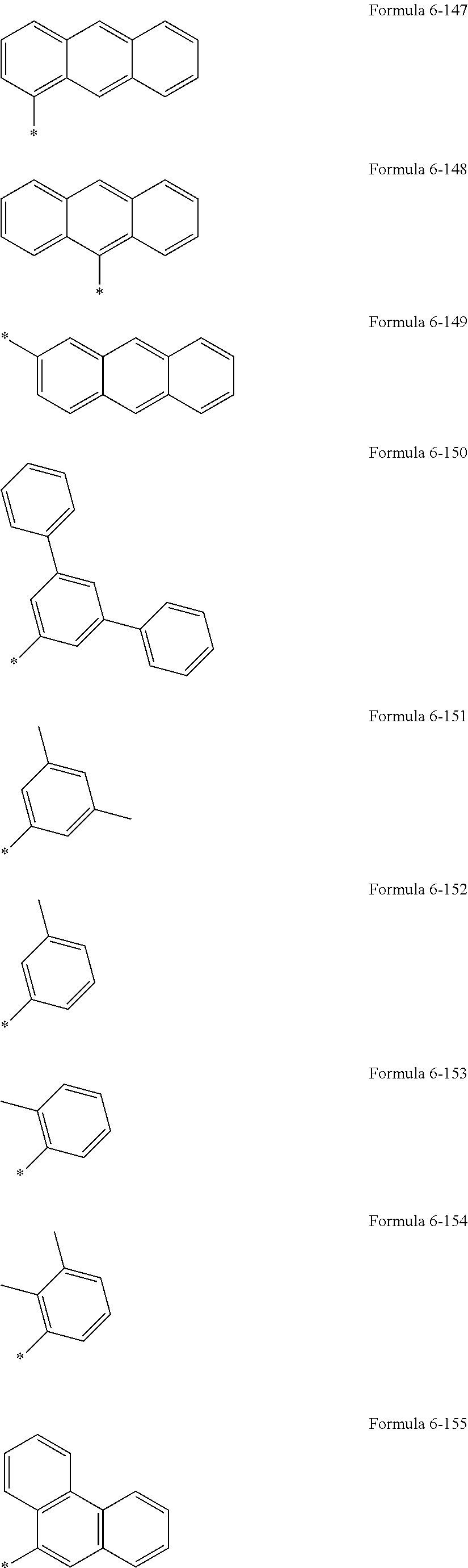


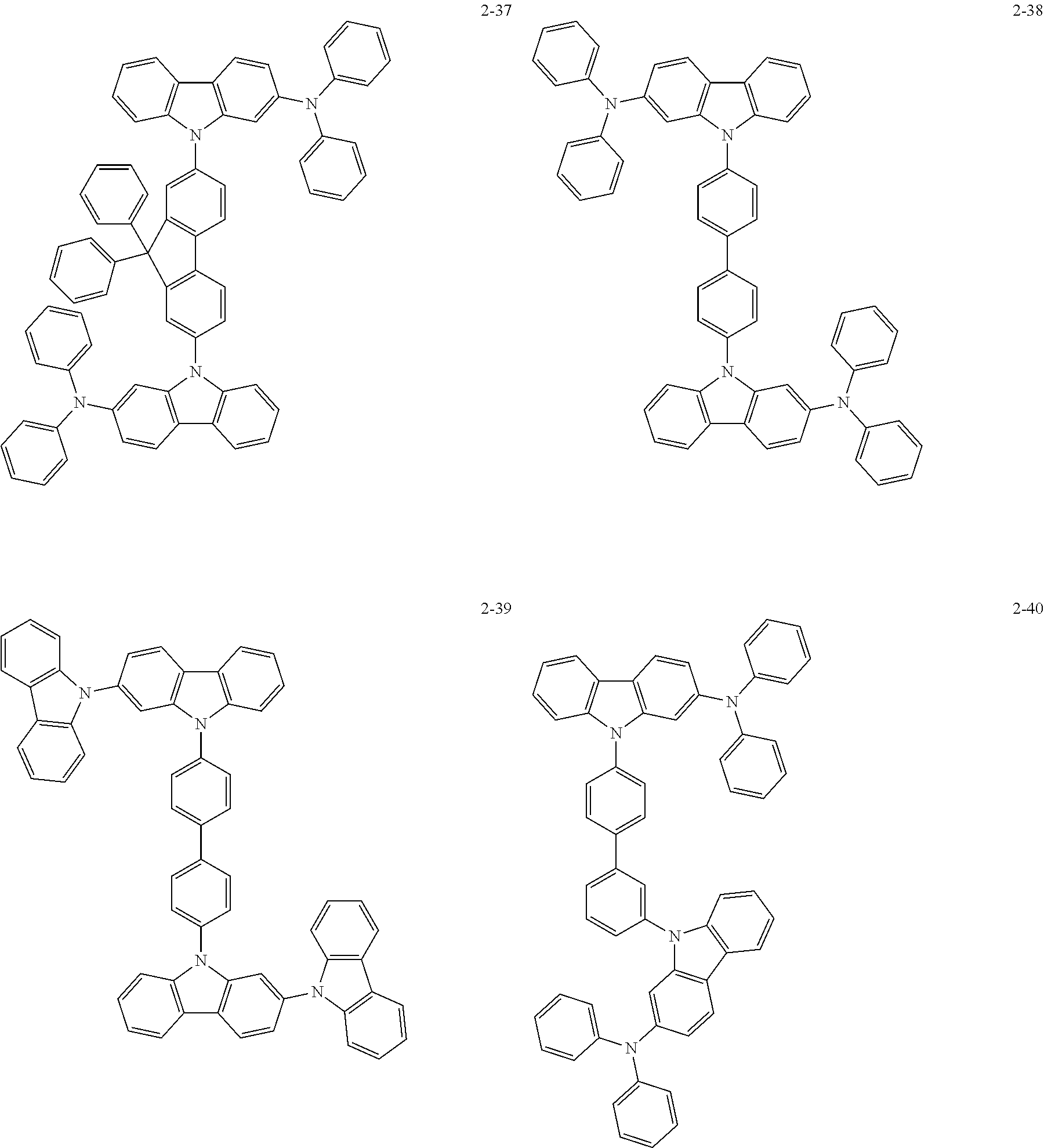


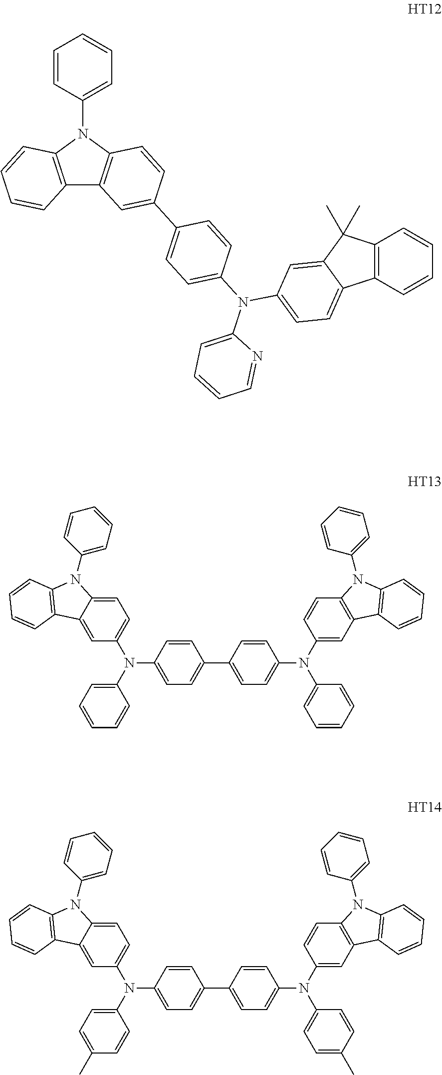


Ar601-[(L601)xe1-E601]xe2, <Formula 601>


| TABLE 1 | |||||
| Driving | Current | ||||
| Hole transport | Emission layer | voltage | density | Efficiency | |
| layer | Host | Dopant | (V) | (mA/cm2) | (cd/A) | |
| Example 1 | Compound 2-2 | Compound 1-22 | Compound | 4.5 | 10 | 38.5 |
| PD76 | ||||||
| Example 2 | Compound 2-7 | Compound 1-24 | Compound | 4.3 | 10 | 36.2 |
| PD76 | ||||||
| Example 3 | Compound 2-51 | Compound 1-24 | Compound | 4.2 | 10 | 39.3 |
| PD76 | ||||||
| Example 4 | Compound 2-29 | Compound 1-25 | Compound | 4.3 | 10 | 37.7 |
| PD76 | ||||||
| Example 5 | Compound 2-51 | Compound 1-23 | Compound | 4.4 | 10 | 38.1 |
| PD76 | ||||||
| Comparative | Compound A1 | Compound 1-23 | Compound | 4.8 | 10 | 31.7 |
| Example 1 | PD76 | |||||
| Comparative | Compound 2-2 | Alq3 | Compound | 6.2 | 10 | 17.6 |
| Example 2 | PD76 | |||||
 |
||||||
 |
||||||
 |
||||||
 |
||||||
 |
||||||
 |
||||||
 |
||||||
 |
||||||
 |
||||||
Claims (17)


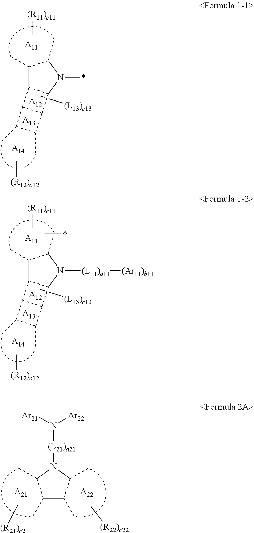


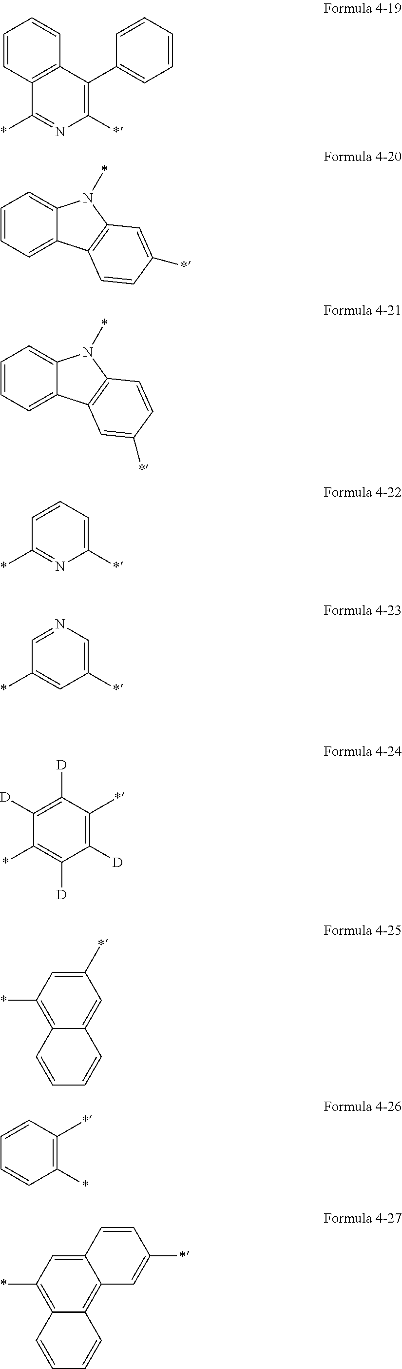


Applications Claiming Priority (2)
| Application Number | Priority Date | Filing Date | Title |
|---|---|---|---|
| KR10-2015-0177363 | 2015-12-11 | ||
| KR1020150177363A KR20170070358A (en) | 2015-12-11 | 2015-12-11 | Organic light emitting device |
Publications (2)
| Publication Number | Publication Date |
|---|---|
| US20170170404A1 US20170170404A1 (en) | 2017-06-15 |
| US11653563B2 true US11653563B2 (en) | 2023-05-16 |
Family
ID=59018243
Family Applications (1)
| Application Number | Title | Priority Date | Filing Date |
|---|---|---|---|
| US15/374,170 Active 2038-12-25 US11653563B2 (en) | 2015-12-11 | 2016-12-09 | Organic light-emitting device |
Country Status (2)
| Country | Link |
|---|---|
| US (1) | US11653563B2 (en) |
| KR (2) | KR20170070358A (en) |
Families Citing this family (3)
| Publication number | Priority date | Publication date | Assignee | Title |
|---|---|---|---|---|
| KR20170070358A (en) | 2015-12-11 | 2017-06-22 | 삼성디스플레이 주식회사 | Organic light emitting device |
| WO2017204556A1 (en) * | 2016-05-26 | 2017-11-30 | 덕산네오룩스 주식회사 | Compound for organic electronic element, organic electronic element using same and electronic device therefor |
| KR102146386B1 (en) * | 2018-07-11 | 2020-08-20 | 한국화학연구원 | Composistion for organic electroluminescent device and novel organic electroluminescent and organic electroluminescent device comprising the same |
Citations (12)
| Publication number | Priority date | Publication date | Assignee | Title |
|---|---|---|---|---|
| KR20110066766A (en) | 2009-12-11 | 2011-06-17 | 덕산하이메탈(주) | Compound containing five-membered heterocyclic ring, organic electric device using same, and terminal thereof |
| KR20120088752A (en) | 2009-10-20 | 2012-08-08 | 토소가부시키가이샤 | Carbazole compound and use thereof |
| KR20130083817A (en) | 2012-01-13 | 2013-07-23 | 덕산하이메탈(주) | Compound for organic electronic element, organic electronic element using the same, and a electronic device thereof |
| KR20130134202A (en) | 2012-05-30 | 2013-12-10 | 롬엔드하스전자재료코리아유한회사 | Novel organic electroluminescence compounds and organic electroluminescence device containing the same |
| US20140319472A1 (en) * | 2013-04-23 | 2014-10-30 | Samsung Display Co., Ltd. | Organic light-emitting diode |
| US20140326987A1 (en) * | 2011-11-28 | 2014-11-06 | Duksan High Metal Co., Ltd. | Compound for organic electronic element, organic electronic element using the same and electronic device thereof |
| KR20140142021A (en) * | 2013-06-03 | 2014-12-11 | 덕산하이메탈(주) | An organic electronic element comprising a layer for improving light efficiency, and an electronic device comprising the same |
| US20150001511A1 (en) | 2013-07-01 | 2015-01-01 | Samsung Display Co., Ltd. | Organic light-emitting device |
| WO2015037965A1 (en) * | 2013-09-16 | 2015-03-19 | Rohm And Haas Electronic Materials Korea Ltd. | Novel organic electroluminescent compounds and organic electroluminescent device comprising the same |
| US20160028020A1 (en) * | 2014-07-24 | 2016-01-28 | Duk San Neolux Co., Ltd. | Organic electronic element and an electronic device comprising it |
| US20170117486A1 (en) * | 2015-10-27 | 2017-04-27 | Samsung Display Co., Ltd. | Organic light-emitting device |
| US20170170404A1 (en) | 2015-12-11 | 2017-06-15 | Samsung Display Co., Ltd. | Organic light-emitting device |
-
2015
- 2015-12-11 KR KR1020150177363A patent/KR20170070358A/en not_active Ceased
-
2016
- 2016-12-09 US US15/374,170 patent/US11653563B2/en active Active
-
2023
- 2023-09-04 KR KR1020230117206A patent/KR20230130598A/en not_active Withdrawn
Patent Citations (18)
| Publication number | Priority date | Publication date | Assignee | Title |
|---|---|---|---|---|
| KR20120088752A (en) | 2009-10-20 | 2012-08-08 | 토소가부시키가이샤 | Carbazole compound and use thereof |
| US20120203010A1 (en) * | 2009-10-20 | 2012-08-09 | Tosoh Corporation | Carbazole compound and use thereof |
| KR20110066766A (en) | 2009-12-11 | 2011-06-17 | 덕산하이메탈(주) | Compound containing five-membered heterocyclic ring, organic electric device using same, and terminal thereof |
| US20140326987A1 (en) * | 2011-11-28 | 2014-11-06 | Duksan High Metal Co., Ltd. | Compound for organic electronic element, organic electronic element using the same and electronic device thereof |
| KR20130083817A (en) | 2012-01-13 | 2013-07-23 | 덕산하이메탈(주) | Compound for organic electronic element, organic electronic element using the same, and a electronic device thereof |
| US20150155498A1 (en) | 2012-05-30 | 2015-06-04 | Rohm And Haas Electronic Materials Korea Ltd. | Novel organic electroluminescence compounds and organic electroluminescence device containing the same |
| KR20130134202A (en) | 2012-05-30 | 2013-12-10 | 롬엔드하스전자재료코리아유한회사 | Novel organic electroluminescence compounds and organic electroluminescence device containing the same |
| KR20140126610A (en) | 2013-04-23 | 2014-10-31 | 삼성디스플레이 주식회사 | Organic light emitting diode |
| US20140319472A1 (en) * | 2013-04-23 | 2014-10-30 | Samsung Display Co., Ltd. | Organic light-emitting diode |
| KR20140142021A (en) * | 2013-06-03 | 2014-12-11 | 덕산하이메탈(주) | An organic electronic element comprising a layer for improving light efficiency, and an electronic device comprising the same |
| US20150001511A1 (en) | 2013-07-01 | 2015-01-01 | Samsung Display Co., Ltd. | Organic light-emitting device |
| KR20150003566A (en) | 2013-07-01 | 2015-01-09 | 삼성디스플레이 주식회사 | Organic light emitting diodes |
| WO2015037965A1 (en) * | 2013-09-16 | 2015-03-19 | Rohm And Haas Electronic Materials Korea Ltd. | Novel organic electroluminescent compounds and organic electroluminescent device comprising the same |
| US20160028020A1 (en) * | 2014-07-24 | 2016-01-28 | Duk San Neolux Co., Ltd. | Organic electronic element and an electronic device comprising it |
| US20170117486A1 (en) * | 2015-10-27 | 2017-04-27 | Samsung Display Co., Ltd. | Organic light-emitting device |
| KR20170049714A (en) | 2015-10-27 | 2017-05-11 | 삼성디스플레이 주식회사 | An organic light emitting device |
| US20170170404A1 (en) | 2015-12-11 | 2017-06-15 | Samsung Display Co., Ltd. | Organic light-emitting device |
| KR20170070358A (en) | 2015-12-11 | 2017-06-22 | 삼성디스플레이 주식회사 | Organic light emitting device |
Also Published As
| Publication number | Publication date |
|---|---|
| US20170170404A1 (en) | 2017-06-15 |
| KR20170070358A (en) | 2017-06-22 |
| KR20230130598A (en) | 2023-09-12 |
Similar Documents
| Publication | Publication Date | Title |
|---|---|---|
| US12336426B2 (en) | Organic light-emitting device | |
| US10665789B2 (en) | Organic light-emitting device | |
| US9172046B1 (en) | Organic light-emitting device | |
| US9896621B2 (en) | Organic light-emitting device | |
| US9972789B2 (en) | Organic light-emitting device | |
| US10333074B2 (en) | Organic light-emitting device | |
| US20190115538A1 (en) | Organic light-emitting device and flat display apparatus including the same | |
| US20170125697A1 (en) | Organic light-emitting device | |
| US9917262B2 (en) | Organic light-emitting device | |
| US11944003B2 (en) | Organic light-emitting device | |
| US20160111663A1 (en) | Organic light-emitting device | |
| US20150053933A1 (en) | Organic light-emitting device | |
| US10978643B2 (en) | Organic light-emitting device | |
| US10825993B2 (en) | Organic light-emitting device and method of manufacturing the same | |
| US11038113B2 (en) | Organic light-emitting device | |
| US12376490B2 (en) | Organic light-emitting device | |
| US20170054091A1 (en) | Organic light-emitting device | |
| US9859503B2 (en) | Organic light-emitting device | |
| US20170133599A1 (en) | Organic light-emitting device | |
| US10361372B2 (en) | Organic light-emitting device | |
| US10186666B2 (en) | Condensed-cyclic compound and organic light emitting device including the same | |
| US20170125690A1 (en) | Organic light-emitting device | |
| US10032994B2 (en) | Organic light-emitting device | |
| US11653563B2 (en) | Organic light-emitting device | |
| US20170155054A1 (en) | Organic light-emitting device |
Legal Events
| Date | Code | Title | Description |
|---|---|---|---|
| AS | Assignment |
Owner name: SAMSUNG DISPLAY CO., LTD., KOREA, REPUBLIC OF Free format text: ASSIGNMENT OF ASSIGNORS INTEREST;ASSIGNORS:KIM, MYEONG-SUK;KIM, HEE-YEON;CHO, HWAN-HEE;AND OTHERS;REEL/FRAME:040699/0907 Effective date: 20161208 |
|
| STPP | Information on status: patent application and granting procedure in general |
Free format text: DOCKETED NEW CASE - READY FOR EXAMINATION |
|
| STPP | Information on status: patent application and granting procedure in general |
Free format text: NON FINAL ACTION MAILED |
|
| STPP | Information on status: patent application and granting procedure in general |
Free format text: RESPONSE TO NON-FINAL OFFICE ACTION ENTERED AND FORWARDED TO EXAMINER |
|
| STPP | Information on status: patent application and granting procedure in general |
Free format text: FINAL REJECTION MAILED |
|
| STPP | Information on status: patent application and granting procedure in general |
Free format text: RESPONSE AFTER FINAL ACTION FORWARDED TO EXAMINER |
|
| STPP | Information on status: patent application and granting procedure in general |
Free format text: DOCKETED NEW CASE - READY FOR EXAMINATION |
|
| STPP | Information on status: patent application and granting procedure in general |
Free format text: NON FINAL ACTION MAILED |
|
| STPP | Information on status: patent application and granting procedure in general |
Free format text: FINAL REJECTION MAILED |
|
| STPP | Information on status: patent application and granting procedure in general |
Free format text: DOCKETED NEW CASE - READY FOR EXAMINATION |
|
| STPP | Information on status: patent application and granting procedure in general |
Free format text: NON FINAL ACTION MAILED |
|
| STPP | Information on status: patent application and granting procedure in general |
Free format text: RESPONSE TO NON-FINAL OFFICE ACTION ENTERED AND FORWARDED TO EXAMINER |
|
| STPP | Information on status: patent application and granting procedure in general |
Free format text: NOTICE OF ALLOWANCE MAILED -- APPLICATION RECEIVED IN OFFICE OF PUBLICATIONS |
|
| STCF | Information on status: patent grant |
Free format text: PATENTED CASE |