US11652348B2 - Integrated circuit and an operation method thereof - Google Patents
Integrated circuit and an operation method thereof Download PDFInfo
- Publication number
- US11652348B2 US11652348B2 US17/143,132 US202117143132A US11652348B2 US 11652348 B2 US11652348 B2 US 11652348B2 US 202117143132 A US202117143132 A US 202117143132A US 11652348 B2 US11652348 B2 US 11652348B2
- Authority
- US
- United States
- Prior art keywords
- transistor
- voltage
- coupled
- node
- gate
- Prior art date
- Legal status (The legal status is an assumption and is not a legal conclusion. Google has not performed a legal analysis and makes no representation as to the accuracy of the status listed.)
- Active, expires
Links
Images


Classifications
-
- H—ELECTRICITY
- H02—GENERATION; CONVERSION OR DISTRIBUTION OF ELECTRIC POWER
- H02H—EMERGENCY PROTECTIVE CIRCUIT ARRANGEMENTS
- H02H9/00—Emergency protective circuit arrangements for limiting excess current or voltage without disconnection
- H02H9/04—Emergency protective circuit arrangements for limiting excess current or voltage without disconnection responsive to excess voltage
- H02H9/045—Emergency protective circuit arrangements for limiting excess current or voltage without disconnection responsive to excess voltage adapted to a particular application and not provided for elsewhere
- H02H9/046—Emergency protective circuit arrangements for limiting excess current or voltage without disconnection responsive to excess voltage adapted to a particular application and not provided for elsewhere responsive to excess voltage appearing at terminals of integrated circuits
-
- H—ELECTRICITY
- H03—ELECTRONIC CIRCUITRY
- H03K—PULSE TECHNIQUE
- H03K19/00—Logic circuits, i.e. having at least two inputs acting on one output; Inverting circuits
- H03K19/003—Modifications for increasing the reliability for protection
- H03K19/00315—Modifications for increasing the reliability for protection in field-effect transistor circuits
-
- H—ELECTRICITY
- H10—SEMICONDUCTOR DEVICES; ELECTRIC SOLID-STATE DEVICES NOT OTHERWISE PROVIDED FOR
- H10D—INORGANIC ELECTRIC SEMICONDUCTOR DEVICES
- H10D89/00—Aspects of integrated devices not covered by groups H10D84/00 - H10D88/00
- H10D89/60—Integrated devices comprising arrangements for electrical or thermal protection, e.g. protection circuits against electrostatic discharge [ESD]
- H10D89/601—Integrated devices comprising arrangements for electrical or thermal protection, e.g. protection circuits against electrostatic discharge [ESD] for devices having insulated gate electrodes, e.g. for IGFETs or IGBTs
- H10D89/811—Integrated devices comprising arrangements for electrical or thermal protection, e.g. protection circuits against electrostatic discharge [ESD] for devices having insulated gate electrodes, e.g. for IGFETs or IGBTs using FETs as protective elements
-
- H—ELECTRICITY
- H03—ELECTRONIC CIRCUITRY
- H03K—PULSE TECHNIQUE
- H03K19/00—Logic circuits, i.e. having at least two inputs acting on one output; Inverting circuits
- H03K19/003—Modifications for increasing the reliability for protection
- H03K19/0033—Radiation hardening
- H03K19/00338—In field effect transistor circuits
-
- H—ELECTRICITY
- H03—ELECTRONIC CIRCUITRY
- H03K—PULSE TECHNIQUE
- H03K19/00—Logic circuits, i.e. having at least two inputs acting on one output; Inverting circuits
- H03K19/0175—Coupling arrangements; Interface arrangements
- H03K19/017545—Coupling arrangements; Impedance matching circuits
-
- H—ELECTRICITY
- H03—ELECTRONIC CIRCUITRY
- H03K—PULSE TECHNIQUE
- H03K19/00—Logic circuits, i.e. having at least two inputs acting on one output; Inverting circuits
- H03K19/0175—Coupling arrangements; Interface arrangements
- H03K19/017545—Coupling arrangements; Impedance matching circuits
- H03K19/017572—Coupling arrangements; Impedance matching circuits using opto-electronic devices
-
- H—ELECTRICITY
- H03—ELECTRONIC CIRCUITRY
- H03K—PULSE TECHNIQUE
- H03K19/00—Logic circuits, i.e. having at least two inputs acting on one output; Inverting circuits
- H03K19/0175—Coupling arrangements; Interface arrangements
- H03K19/0185—Coupling arrangements; Interface arrangements using field effect transistors only
- H03K19/018557—Coupling arrangements; Impedance matching circuits
-
- H—ELECTRICITY
- H03—ELECTRONIC CIRCUITRY
- H03K—PULSE TECHNIQUE
- H03K17/00—Electronic switching or gating, i.e. not by contact-making and –breaking
- H03K17/51—Electronic switching or gating, i.e. not by contact-making and –breaking characterised by the components used
- H03K17/56—Electronic switching or gating, i.e. not by contact-making and –breaking characterised by the components used by the use, as active elements, of semiconductor devices
Definitions
- De-coupling capacitance circuit is configured as an essential component for stabilization of power supply voltages in standard cell circuits of integrated circuit operating in high speed. Nonetheless, as the thickness of gate oxide layers in transistors of the integrated circuits develops to get thinner, the de-coupling capacitance circuit is exposed in higher risk of electrostatic discharge.
- FIG. 1 A is a schematic diagram of part of an integrated circuit, in accordance with some embodiments.
- FIG. 1 B is a schematic diagram of part of an integrated circuit, in accordance with various embodiments.
- FIG. 2 is detailed schematic diagram corresponding to the integrated circuit in FIG. 1 A , in accordance with some embodiments.
- FIG. 3 is a layout diagram corresponding to the integrated circuit in FIG. 1 A , in accordance with some embodiments.
- FIG. 4 is detailed schematic diagram of an integrated circuit corresponding to the integrated circuit in FIG. 1 A , in accordance with various embodiments.
- FIG. 5 A is a layout diagram corresponding to the integrated circuit in FIG. 4 , in accordance with some embodiments.
- FIG. 5 B is a layout diagram corresponding to the integrated circuit in FIG. 4 , in accordance with various embodiments.
- FIG. 6 is detailed schematic diagram of an integrated circuit of an integrated circuit corresponding to the integrated circuit in FIG. 1 A , in accordance with various embodiments.
- FIG. 7 is detailed schematic diagram of an integrated circuit corresponding to the integrated circuit in FIG. 1 B , in accordance with various embodiments.
- FIG. 8 is a layout diagram corresponding to the integrated circuit in FIG. 7 , in accordance with some embodiments.
- FIG. 9 is detailed schematic diagram of an integrated circuit corresponding to the integrated circuit in FIG. 1 B , in accordance with various embodiments.
- FIG. 10 A is a layout diagram corresponding to the integrated circuit in FIG. 9 , in accordance with some embodiments.
- FIG. 10 B is a layout diagram corresponding to the integrated circuit in FIG. 9 , in accordance with various embodiments.
- FIG. 11 is a flow chart of a method of operating an integrated circuit, in accordance with some embodiments.
- FIG. 12 is a block diagram of a system for designing the integrated circuit layout design, in accordance with some embodiments of the present disclosure.
- FIG. 13 is a block diagram of an integrated circuit manufacturing system, and an integrated circuit manufacturing flow associated therewith, in accordance with some embodiments.
- first and second features are formed in direct contact
- additional features may be formed between the first and second features, such that the first and second features may not be in direct contact
- present disclosure may repeat reference numerals and/or letters in the various examples. This repetition is for the purpose of simplicity and clarity and does not in itself dictate a relationship between the various embodiments and/or configurations discussed.
- spatially relative terms such as “beneath,” “below,” “lower,” “above,” “upper” and the like, may be used herein for ease of description to describe one element or feature's relationship to another element(s) or feature(s) as illustrated in the figures.
- the spatially relative terms are intended to encompass different orientations of the device in use or operation in addition to the orientation depicted in the figures.
- the apparatus may be otherwise oriented (rotated 90 degrees or at other orientations) and the spatially relative descriptors used herein may likewise be interpreted accordingly.
- the term “and/or” includes any and all combinations of one or more of the associated listed items.
- “around”, “about”, “approximately” or “substantially” shall generally refer to any approximate value of a given value or range, in which it is varied depending on various arts in which it pertains, and the scope of which should be accorded with the broadest interpretation understood by the person skilled in the art to which it pertains, so as to encompass all such modifications and similar structures. In some embodiments, it shall generally mean within 20 percent, preferably within 10 percent, and more preferably within 5 percent of a given value or range. Numerical quantities given herein are approximate, meaning that the term “around”, “about”, “approximately” or “substantially” can be inferred if not expressly stated, or meaning other approximate values.
- FIG. 1 A is a schematic diagram of part of an integrated circuit 10 , in accordance with some embodiments.
- the integrated circuit 10 includes a start-up circuit 100 , a capacitive unit 200 , and a capacitive unit 300 .
- the start-up circuit 100 is coupled between the capacitive unit 200 and the capacitive unit 300 .
- the capacitive unit 200 and the capacitive unit 300 are coupled to the supply voltage terminal VSS and the supply voltage terminal VDD respectively.
- the supply voltage terminal VSS provides the supply voltage VSS (i.e., being referred to as a ground providing ground voltage,) and the supply voltage terminal VDD provides the supply voltage VDD.
- the supply voltage VDD has a voltage level greater than the supply voltage VSS.
- the start-up circuit 100 includes a voltage generation circuit 110 , a voltage generation circuit 120 , and a control circuit 130 .
- the voltage generation circuit 110 and the voltage generation circuit 120 are coupled to the capacitive unit 200 at the node N 1 .
- the voltage generation circuit 110 and the voltage generation circuit 120 are coupled to the capacitive unit 300 at the node N 2 .
- the control circuit 130 is coupled between the capacitive unit 200 and the node N 1 .
- the voltage generation circuit 110 is coupled to the supply voltage terminal VDD.
- the voltage generation circuit 120 and the control circuit 130 are coupled to the supply voltage terminal VSS.
- the control circuit 130 is coupled between the supply voltage terminal VSS and the voltage generation circuit 120 .
- integrated circuit 10 is configured to operate as a de-couping circuit.
- the control circuit 130 is configured to generate an initiation voltage at the node N 1 .
- the voltage generation circuit 110 transmits, in response to the initiation voltage at the node N 1 , the supply voltage VDD from the supply voltage terminal VDD to the voltage generation circuit 120 . Consequently, the voltage generation circuit 120 transmits, in response to the supply voltage VDD from the voltage generation circuit 110 , the supply voltage VSS different from the supply voltage VDD to the node N 1 .
- the voltage level of the node N 1 is pulled down from the initiation voltage to the supply voltage VSS by the voltage generation circuit 120 .
- the voltage generation circuit 120 is a pull down circuit.
- the start-up circuit 100 is configured to output the voltage level of the node N 1 as the control signal CS 1 to the capacitive unit 200 , and to output the voltage level of the node N 2 as the control signal CS 2 to the capacitive unit 300 .
- the capacitive unit 200 and the capacitive unit 300 receive the control signal CS 1 and CS 2 from the start-up circuit 100 to operate separately.
- the voltage generation circuit 110 pulls up the voltage level of the node N 2 to the supply voltage VDD
- the voltage generation circuit 120 pulls down the voltage level of the node N 1 to the supply voltage VSS
- there is significant voltage difference between two terminals of each of the capacitive unit 200 and the capacitive unit 300 Accordingly, the capacitive unit 200 and the capacitive unit 300 have high capacitance values. The details of operations of the integrated circuit 10 will be discussed in the following paragraphs.
- the voltage generation circuit 110 is further configured to generate based on the supply voltage VDD, in response to the initiation voltage generated by the control circuit 130 , the control signal CS 2 to the voltage generation circuit 120 .
- the voltage generation circuit 120 is configured to generate based on the supply voltage VSS, in response to the control signal CS 2 received from the voltage generation circuit 110 , the control signal CS 1 to the node N 1 .
- FIG. 1 B is a schematic diagram of part of the integrated circuit 10 , in accordance with various embodiments. With respect to the embodiments of FIG. 1 A , like elements in FIG. 1 B are designated with the same reference numbers for ease of understanding. The specific operations of similar elements, which are already discussed in detail in above paragraphs, are omitted herein for the sake of brevity.
- the control circuit 130 in FIG. 1 B is coupled between the node N 2 and the capacitive unit 300 .
- the control circuit 130 is configured to generate the initiation voltage at the node N 2 .
- the voltage generation circuit 120 transmits, in response to the initiation voltage at the node N 2 , the supply voltage VSS from the supply voltage terminal VSS to the voltage generation circuit 110 . Consequently, the voltage generation circuit 110 transmits, in response to the supply voltage VSS from the voltage generation circuit 120 , the supply voltage VSS different from the supply voltage VDD to the node N 2 .
- the voltage level of the node N 2 is pulled up from the initiation voltage to the supply voltage VDD by the voltage generation circuit 110 .
- the voltage generation circuit 110 is a pull up circuit.
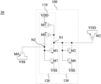
- FIG. 2 is detailed schematic diagram corresponding to the integrated circuit 10 in FIG. 1 A , in accordance with some embodiments.
- the voltage generation circuit 110 in the start-up circuit 100 includes a P-type transistor M 0 .
- the voltage generation circuit 120 includes an N-type transistor M 1 .
- the control circuit 130 includes an N-type transistor M 2 .
- the transistors M 0 -M 2 are implemented by metal-oxide-semiconductor field-effect transistors (MOSFET).
- a gate of the transistor M 0 is coupled to the node N 1 , a source of the transistor M 0 is coupled to the supply voltage VDD, and the source of the transistor M 0 is coupled to the node N 2 .
- a gate of the transistor M 1 is coupled to the node N 2 , a source of the transistor M 1 is coupled to the supply voltage VSS, and a drain of the transistor M 1 is coupled to the node N 1 .
- a gate and a source of the transistor M 2 are coupled to the node N 1 , and a source of the transistor M 2 is coupled to the supply voltage VSS.
- the capacitive unit 200 includes a P-type transistor M 3 and the capacitive unit 300 includes an N-type transistor M 4 .
- a gate of the transistor M 3 is coupled the transistors M 0 -M 2 at the node N 1 , and a source and a drain of the transistor M 3 and the supply voltage terminal VDD are coupled with each other.
- a gate of the transistor M 4 and the transistor M 0 -M 2 are coupled at the node N 2 , and a source and a drain of the transistor M 4 and the supply voltage terminal VSS are coupled with each other.
- the transistor M 2 operates as a diode. Specifically, in an initial stage, the transistor M 2 generates at the node N 1 the initiation voltage equal a threshold voltage of the transistor M 2 .
- the initiation voltage is a low voltage level with respect to the supply voltage VDD.
- the control signal CS 1 having the voltage level of the node N 1 is referred to as having a logic value 0. Consequently, the transistor M 0 is turned on in response to the control signal CS 1 which has the logic value 0 (i.e., the voltage level of the node N 1 ) and is received at the gate of the transistor M 0 , and the voltage level of the node N 2 is adjusted based on the supply voltage VDD.
- the voltage level of the node N 2 is the supply voltage VDD
- the control signal CS 2 having the voltage level of the node N 2 is referred to as having a logic value 1.
- the transistor M 1 is turned on in response to the control signal CS 2 which has the logic value 1 (i.e., the voltage level of the node N 2 ) and is received at the gate of the transistor M 1 , and the voltage level of the node N 1 is adjusted based on the supply voltage VSS. Accordingly, the voltage level of the node N 1 is pulled down from the initiation voltage, equal the threshold voltage of the transistor M 2 , to the supply voltage VSS.
- the supply voltage terminal VSS is a ground terminal, and the voltage level of the node N 1 is the voltage level of the ground.
- the transistor M 3 is turned on.
- the control signal CS 2 has the logic value 1
- the transistor M 4 is turned on.
- the voltage generation circuit 110 and the voltage generation circuit 120 provide stable voltages to the nodes N 1 and N 2 , the transistor M 3 and the transistor M 4 have steady gate clamp voltages, occupy meager areas and being de-coupling capacitors with great capacitance.
- the integrated circuit 10 is in an ESD positive-to-VSS mode (i.e., ESD PS mode), and an ESD current between the supply voltage terminal VDD and the supply voltage terminal VSS is discharged by three electrostatic discharge paths P 1 -P 3 .
- ESD PS mode ESD positive-to-VSS mode
- control circuit 130 including the transistor M 2 and the capacitive unit 200 including the transistor M 3 are configured as the electrostatic discharge path P 1 .
- a first portion of the ESD current between the supply voltage terminal VDD and the supply voltage terminal VSS flows out from the drain and the source of the capacitive unit 200 through the gate (i.e., being referred to as the gate oxide layer) thereof, the node N 1 , the drain and the source of the transistor M 2 to the supply voltage terminal VSS.
- the voltage generation circuit 120 including the transistor M 1 and the capacitive unit 200 including the transistor M 3 are configured as the electrostatic discharge path P 2 .
- a second portion of the ESD current between the supply voltage terminal VDD and the supply voltage terminal VSS flows out from the drain and the source of the capacitive unit 200 to the supply voltage terminal VSS through the gate (i.e., being referred to as the gate oxide layer) thereof, the node N 1 , the drain and the source of the transistor M 1 .
- the voltage generation circuit 110 including the transistor M 0 and the capacitive unit 300 including the transistor M 4 are configured as the electrostatic discharge path P 3 .
- a third portion of the ESD current between the supply voltage terminal VDD and the supply voltage terminal VSS flows out from the drain and the source of the transistor M 0 , through the gate (i.e., being referred to as the gate oxide layer) of the capacitive unit 300 and the drain and the source of the capacitive unit 300 to the supply voltage terminal VSS.
- gates of elements, similar to the capacitive units 200 and 300 , in a de-coupling circuit are coupled directly.
- a gate oxide layer has a tendency to get thinner and thinner, a breakdown voltage of a transistor consisting of a capacitive unit declines. Therefore, in those approaches, the de-coupling circuit tends to be struck vulnerably by the ESD current and/or be broken down.
- the gates of the capacitive units 200 and 300 are firstly coupled to the start-up circuit 100 which includes the nodes N 1 and N 2 of an inner network. Accordingly, it avoid the gate oxide layer from being broken down.
- the breakdown voltage as a whole surges around 30% to around 50%.
- gate voltages of the elements are undetermined, and are charged slowly by leakage currents in a relevant network. In such arrangements, it takes a period of time to initiate the circuit.
- the determined initiation voltage i.e., a threshold voltage
- the voltage generation circuits 110 - 120 respond rapidly and generate voltages (having certain logic states) at the nodes N 1 -N 2 . Accordingly, compared with some approaches, the circuit, in one of the embodiments of the present disclosure act quicker than one in some approaches, and no extra charging time is required.
- the start speed of the integrated circuit in one of the embodiments of the present disclosure is around 20% faster than that of some approaches.
- the circuit can only utilize P-type transistors as capacitive units, and extra circuit is needed for using N-type transistors as capacitive units.
- the gate voltages of the elements similar to the capacitive units 200 and 300 are undetermined, and accordingly, significant area is required for increasing the capacitance values of the capacitive units in some approaches. Therefore, the integrated circuit suffers from the area penalty.
- the configurations of the present disclosure include P-type transistors and N-type transistors for capacitive units, and steady gate voltages are provided for the capacitive units. Compared with some approaches, the present disclosure provides greater capacitance values in a smaller area.
- the integrated circuit 10 is in an ESD negative-to-VDD mode (ESD ND mode), the ESD current between the supply voltage terminal VDD and the supply voltage terminal VSS is also discharge in the aforementioned electrostatic discharge path P 1 -P 3 .
- ESD ND mode ESD negative-to-VDD mode
- the flowing direction of the ESD current in the ESD ND mode is contrary to that in the PS mode, while other configurations are similar. Accordingly, the repetitious descriptions are omitted herein.
- FIG. 3 is a layout diagram corresponding to the integrated circuit 10 in FIG. 1 A , in accordance with some embodiments. With respect to the embodiments of FIGS. 1 A- 2 , like elements in FIG. 3 are designated with the same reference numbers for ease of understanding.
- the integrated circuit 10 includes active regions (i.e., oxide device) 301 - 307 , gates (i.e., Poly) 401 - 409 , conductive segments (i.e., metal on diffusion, MD) 501 - 507 , conductive lines (i.e., metal zero layer, M 0 ) 601 - 604 and vias VD 1 -VD 14 , VG 1 -VG 5 .
- the active region 301 - 307 are arranged in a first layer
- the gates 401 - 409 and the conductive segments 501 - 507 are arranged in a second layer above the first layer.
- the conductive lines 601 - 604 are arranged in a third layer above the second layer.
- the vias VD 1 -VD 14 are arranged between the first layer and the second layer or between the second layer and the third layer.
- the vias VG 1 -VG 5 are arranged between the second layer and the third layer.
- the gate 402 corresponds to the gate of the transistor M 3
- the conductive segment 501 corresponds to the drain/source of the transistor M 3
- the conductive segment 502 corresponds to the source/drain of the transistor M 3 and the source of the transistor M 0
- the gate 403 corresponds to the gate of the transistor M 0
- the conductive segment 503 corresponds to the drain of the transistor M 0
- the gate 406 corresponds to the gate of the transistor M 4
- the conductive segment 504 corresponds to the drain/source of the transistor M 4
- the conductive segment 505 corresponds to the source/drain of the transistor M 4 and the source of the transistor M 1 .
- the gate 407 corresponds to the gate of the transistor M 1
- the conductive segment 506 corresponds to the drain of the transistor M 1 and the drain of the transistor M 2
- the gate 408 corresponds to the gate of the transistor M 2
- the conductive segment 507 corresponds to the source of the transistor M 2
- the gates 401 , 404 , 405 , and 409 are configured as dummy gates, in which in some embodiments, “dummy gate” are referred to as being not electrically connected as the gate for MOS devices, having no function in the circuit.
- the active regions 301 - 307 extend in x direction.
- the active regions 301 - 303 are included in an active area arranged in an N-type well (NW), in which the N-type is arranged on a substrate (not shown).
- the active regions 304 - 307 are arranged on the substrate or in another active area arranged in a P-type well.
- the gates 401 - 409 extend in y direction.
- the gates 401 - 404 are separated from each other in x direction, and the gates 405 - 409 are separated from each other in x direction.
- the gate 402 is arranged between the active regions 301 and 302 .
- the gate 403 is arranged between the active region 302 and 303 .
- the gate 406 is arranged between the active region 304 and 305 .
- the gate 407 is arranged between the active region 305 and 306 .
- the gate 408 is arranged between the active region 306 and 307 .
- the gates 401 - 404 in a layout diagram crosses over the active area including the active regions 301 - 303
- the gates 405 - 409 in the layout diagram crosses the active area including the active regions 304 - 307 .
- the conductive segments 501 - 507 extend in y direction.
- the conductive segment 501 crosses the active region 301
- the conductive segment 502 crosses the active region 302
- the conductive segment 503 crosses the active region 303
- the conductive segment 504 crosses the active region 304
- the conductive segment 505 crosses the active region 305
- the conductive segment 506 crosses the active region 306
- the conductive segment 507 crosses the active region 307 .
- the conductive lines 601 - 604 extend in x direction, and are separated from each other in y direction. In some embodiments, the conductive lines 601 and 602 are configured to transmit the supply voltages VDD and VSS, respectively, to the integrated circuit 10 .
- the conductive line 603 corresponds to the node N 1 .
- the conductive line 604 corresponds to the node N 2 .
- the active region 301 is coupled to the conductive segment 501 by the via VD 5 , and the conductive segment 501 is coupled to the conductive line 601 through the via VD 6 to receive the supply voltage VDD.
- the active region 302 is coupled to the conductive segment 502 through the via VD 3 , and the conductive segment 502 is coupled to the conductive line 601 through the via VD 4 to receive the supply voltage VDD.
- the gate 402 is coupled to the conductive line 603 through the via VG 2 .
- the drain and the source of the transistor M 3 and the drain of the transistor M 0 are coupled to the supply voltage terminal VDD, and the gate of the transistor M 3 is coupled to the node N 1 .
- the gate 403 is coupled to the conductive line 603 through the via VG 1 .
- the active region 303 is coupled to the conductive segment 503 through the via VD 1 , and the conductive segment 503 is coupled to the conductive line 604 through the via VD 2 .
- the drain of the transistor M 0 is coupled to the node N 2 and the gate of the transistor M 0 is coupled to the node N 1 .
- the active region 304 is coupled to the conductive segment 504 through the via VD 13 , and the conductive segment 504 is coupled to the conductive line 602 through the via VD 14 to receive the supply voltage VSS.
- the active region 305 is coupled to the conductive segment 505 through the via VD 11 , and the conductive segment 505 is coupled to the conductive line 602 through the via VD 12 to receive the supply voltage VSS.
- the gate 406 is coupled to the conductive line 604 through the via VG 5 .
- the drain and the source of the transistor M 4 and the source of the transistor M 1 are coupled to the supply voltage terminal VSS, and the gate of the transistor M 4 is coupled to the node N 2 .
- the gate 407 is coupled to the conductive line 604 through the via VG 4 .
- the active region 306 is coupled to the conductive segment 506 through the via VD 8 , and the conductive segment 506 is coupled to the conductive line 603 through the via VD 7 .
- the source of the transistor M 1 is coupled to the node N 1 and the gate of the transistor M 1 is coupled to the node N 2 .
- the gate 408 is coupled to the conductive line 603 through the via VG 3 .
- the active region 307 is coupled to the conductive segment 507 through the via VD 9 , and the conductive segment 507 is coupled to the conductive line 602 through the via VD 10 .
- the gate of the transistor M 2 is coupled to the node N 1 and the gate of the transistor M 2 is coupled to the supply voltage terminal VSS.
- a portion of the ESD current between the supply voltage terminal VDD and the supply voltage terminal VSS is discharged by the semiconductor structure of the transistors M 1 -M 3 and the conductive line 603 .
- another portion of the ESD current is discharged by the transistors M 0 , M 4 and the conductive line 604 .
- FIG. 3 The configurations of FIG. 3 are given for illustrative purposes. Various implements are within the contemplated scope of the present disclosure. For example, in some embodiments, according to the actual requirement of ESD protection, at least two of the transistors M 0 -M 4 do not share active regions.
- FIG. 4 is detailed schematic diagram of an integrated circuit 20 corresponding to the integrated circuit 10 in FIG. 1 A , in accordance with various embodiments.
- the integrated circuit 20 is configured with respect to, for example, the integrated circuit 10 .
- like elements in FIG. 4 are designated with the same reference numbers for ease of understanding.
- each of the voltage generation circuit 110 , the voltage generation circuit 120 and the control circuit 130 in the integrated circuit 20 further includes multiple transistors coupled in series.
- the voltage generation circuit 110 further includes a P-type transistor M 5 coupled in series with the transistor M 0 .
- the voltage generation circuit 120 further includes an N-type transistor M 5 coupled in series with the transistor M 1 .
- the control circuit 130 further includes an N-type transistor M 6 coupled in series with the transistor M 2 .
- a gate of the transistor M 5 and a gate of the transistor M 0 coupled at the node N 1 .
- the source of the transistor M 0 is coupled to and the drain of the transistor M 5
- the source of the transistor M 5 is coupled to the supply voltage terminal VDD.
- the gate of the transistor M 6 and the gate of the transistor M 1 are coupled at the node N 2 .
- the source of the transistor M 1 being directly coupled to the supply voltage terminal VSS, in FIG.
- the source of the transistor M 1 is coupled to the drain of the transistor M 6 , and the source of the transistor M 6 is coupled to the supply voltage terminal VSS.
- the gate of the transistor M 7 and the gate of the transistor M 2 are coupled at the node N 1 .
- the source of the transistor M 2 is coupled to the drain of the transistor M 7 , and the source of the transistor M 7 is coupled to the supply voltage terminal VSS.
- the voltage generation circuit 110 , the voltage generation circuit 120 , and the control circuit 130 form as a multiple-stage circuit by including multiple transistors in order to meet the requirements of ESD protection capacity while operating the integrated circuit 20 .
- a break down voltage of the integrated circuit 20 increases 1.0 Volts.
- each of the voltage generation circuit 110 , the voltage generation circuit 120 and the control circuit 130 of the integrated circuit 20 includes more than two transistors coupled in series with each other.
- FIG. 5 A is a layout diagram corresponding to the integrated circuit 20 in FIG. 4 , in accordance with some embodiments. With respect to the embodiments of FIGS. 1 A- 4 , like elements in FIG. 5 A are designated with the same reference numbers for ease of understanding.
- the integrated circuit 20 further includes active regions 308 - 311 , gates 410 - 413 , a conductive segment 510 and vias VD 15 -VD 16 .
- the active regions 308 - 311 are configured with respect to, for example, the active region 303 .
- the gates 410 - 413 are configured with respect to, for example, the gate 403 .
- the gate 413 is configured as a dummy gate.
- the conductive segment 510 is configured with respect to, for example, the conductive segment 505 .
- the vias VD 15 -VD 16 are configured with respect to, for example, the via VD 14 .
- the active region 302 corresponds to the source of the transistor M 5
- the gate 410 corresponds to the gate of the transistor M 5
- the active region 308 corresponds to the drain of the transistor M 5 and the source of the transistor M 0
- the gate 410 is coupled to the conductive line 603 through the via VG 6 . Accordingly, the gate of the transistor M 5 is coupled to the node N 1 , the source of the transistor M 5 is coupled to the supply voltage terminal VDD, and the drain of the transistor M 5 is coupled to the gate of the transistor M 0 .
- the active region 305 corresponds to the source of the transistor M 6
- the gate 411 corresponds to the source of the transistor M 6
- the active region 309 corresponds to the gate of the transistor M 6 and the drain of the transistor M 1 .
- the gate 411 is coupled to the conductive line 604 through the via VG 7 . Accordingly, the gate of the transistor M 6 is coupled to the node N 2 , the source of the transistor M 6 is coupled to the supply voltage terminal VSS, and the drain of the transistor M 6 is coupled to the gate of the transistor M 1 .
- the active region 311 corresponds to the source of the transistor M 7
- the gate 412 corresponds to the gate of the transistor M 7
- the active region 310 corresponds to the drain of the transistor M 7 and the source of the transistor M 2 .
- the gate 412 is coupled to the conductive line 603 through the via VG 8 .
- the active region 311 is coupled to the conductive segment 510 through the via VD 13
- the conductive segment 510 is coupled to the conductive line 602 through the via VD 16 . Accordingly, the gate of the transistor M 7 is coupled to the node N 1 , the source of the transistor M 7 is coupled to the supply voltage terminal VSS, and the drain of the transistor M 7 is coupled to the source of the transistor M 2 .
- FIG. 5 B is a layout diagram corresponding to the integrated circuit 20 in FIG. 4 , in accordance with various embodiments. With respect to the embodiments of FIGS. 1 A- 5 A , like elements in FIG. 5 B are designated with the same reference numbers for ease of understanding.
- the integrated circuit 20 further includes active regions 308 a - 308 b , 309 a - 309 b , 310 a - 310 b , gates 414 - 419 , conductive segments 511 - 513 and vias VD 17 - 22 .
- the active regions 308 a - 308 b correspond to a first portion and a second portion of the active region 308 in FIG. 5 A .
- the active regions 309 a - 309 b correspond to a first portion and a second portion of the active region 309 in FIG. 5 A .
- the active regions 310 a - 310 b correspond to a first portion and a second portion of the active region 310 in FIG. 5 A .
- the gates 414 - 419 are configured with respect to, for example, the gate 413 . In some embodiments, the gates 414 - 419 are dummy gates.
- the conductive segments 511 - 513 are configured with respect to, for example, the conductive segment 503 .
- the vias VD 17 -VD 22 are configured with respect to, for example, the via VD 1 .
- the gates 414 - 415 are not electrically connected with the conductive segment 511 .
- the gates 416 - 417 are not electrically connected with the conductive segment 512 .
- the gates 418 - 419 are not electrically connected with the conductive segment 513 .
- the active region 308 a corresponds to the drain of the transistor M 5
- the active region 308 b corresponds to the source of the transistor M 0
- the active regions 308 a - 308 b are separated from each other in x direction.
- the transistors M 0 and M 5 do not share the active region, are referred to as having structures of separated active regions (separate OD).
- the ESD resistance performance of the integrated circuit 20 is enhanced by around 20%. In various embodiments, the occupied area of separated active regions and the ESD resistance performance are considered comprehensively in designing the integrated circuit 20 .
- the active region 309 a corresponds to the drain of the transistor M 6
- the active region 309 b corresponds to the source of the transistor M 1 .
- the active regions 309 a - 309 b are separated from each other in x direction. Alternatively stated, the transistors M 1 and M 6 do not share the active region.
- the active region 310 a corresponds to the drain of the transistor M 7
- the active region 310 b corresponds to the source of the transistor M 2 .
- the active regions 310 a - 310 b are separated from each other in x direction. Alternatively stated, the transistors M 2 and M 7 do not share the active region.
- FIGS. 5 A- 5 B are given for illustrative purposes.
- Various implements are within the contemplated scope of the present disclosure.
- the structure design of separated active regions is adapted for all of active regions in the integrated circuit 20 .
- FIG. 6 is detailed schematic diagram of an integrated circuit 30 corresponding to the integrated circuit 10 in FIG. 1 A , in accordance with various embodiments. With respect to the embodiments of FIGS. 1 A- 5 B , like elements in FIG. 6 are designated with the same reference numbers for ease of understanding.
- the integrated circuit 30 further includes a P-type transistor M 8 .
- a drain of the transistor M 8 is coupled to the source of the transistor M 5
- a source of the transistor M 8 is coupled to the supply voltage terminal VDD
- the gate of the transistor M 8 is coupled to the gates of the transistors M 5 and M 0 at the node N 1 .
- a number of P-type transistors in the voltage generation circuit 110 is different from a number of N-type transistors in the voltage generation circuit 120 and a number of N-type transistors in the control circuit 130 .
- the voltage generation circuit 110 includes three P-type transistors, and the voltage generation circuit 120 and the control circuit 130 includes two N-type transistors respectively.
- the number of P-type transistors in the voltage generation circuit 110 is different from a sum of the number of N-type transistors in the voltage generation circuit 120 and the number of N-type transistors in the control circuit 130 . As shown in the embodiments of FIG. 6 , the number of N-type transistors in the voltage generation circuit 120 and the control circuit 130 is greater than the number of P-type transistors in the voltage generation circuit 110 . In some embodiments, due to the manufacture process and physical properties, the N-type transistors' tolerance to ESD is lower than that of the P-type transistors. Therefore, the start-up circuit 100 includes fewer P-type transistors and also meets the ESD performance requirements of the integrated circuit 30 .
- the voltage generation circuit 110 and the voltage generation circuit 120 of the integrated circuit 30 include the same quantity of transistors, for example, three N-type transistors.
- FIG. 7 is detailed schematic diagram of an integrated circuit 40 corresponding to the integrated circuit 10 in FIG. 1 B , in accordance with various embodiments. With respect to the embodiments of FIGS. 1 A- 6 , like elements in FIG. 7 are designated with the same reference numbers for ease of understanding.
- the control circuit 130 includes a P-type transistor M 9 .
- a gate and a drain of the transistor M 9 are coupled the node N 2 .
- the source of the transistor M 9 is coupled the supply voltage terminal VDD.
- the control circuit 130 is configured to provide the initiation voltage at the node N 2 .
- the transistor M 9 operates as a diode. Specifically, in the initiation stage, the transistor M 9 generates the initiation voltage at the node N 2 , in which the initiation voltage is associated with a threshold voltage (i.e., Vth) of the transistor M 9 and the supply voltage VDD, being the supply voltage VDD subtracts the threshold voltage of the transistor M 9 (VDD-Vth).
- Vth threshold voltage
- VDD the threshold voltage of the transistor M 9
- the initiation voltage is a high voltage level with respect to the supply voltage VSS.
- the control signal CS 2 having the voltage level of the node N 2 is referred to as having the logic value 1. Consequently, the transistor M 1 is turned on in response to the control signal CS 2 which has the logic value 1 (i.e., the voltage level of the node N 2 ) and is received at the gate of the transistor M 1 , and the voltage level of the node N 1 is adjusted based on the supply voltage VSS.
- the voltage level of the node N 1 is the supply voltage VSS
- the control signal CS 1 having the voltage level of the node N 1 is referred to as having the logic value 0.
- the transistor M 0 is turned on in response to the control signal CS 1 which has the logic value 0 (i.e., the voltage level of the node N 1 ) and is received at the gate of the transistor M 0 , and the voltage level of the node N 2 is adjusted based on the supply voltage VDD. Accordingly, the voltage level of the node N 2 is pulled up from the initiation voltage, equal the voltage of VDD-Vth, to the supply voltage VDD.
- the configurations of the integrated circuit 40 of FIG. 7 are similar to the integrated circuit 10 . Hence, the repetitious descriptions are omitted here.
- the ESD current between the supply voltage terminal VDD and the supply voltage terminal VSS is further discharged by the electrostatic discharge path P 4 .
- the control circuit 130 including the transistor M 9 and the capacitive unit 300 including the transistor M 4 are configured as the electrostatic discharge path P 4 .
- Part of the ESD current between the supply voltage terminal VDD and the supply voltage terminal VSS flows out from the supply voltage terminal VDD to the gate (being referred as to the gate oxide layer) of the capacitive unit 300 through the source and the drain of the transistor M 9 and the node N 2 , and further flows to the supply voltage terminal VSS through the source and the drain of the capacitive unit 300 .
- the voltage generation circuit 120 includes multiple N-type transistors, for example, more than two N-type transistors.
- FIG. 8 is a layout diagram corresponding to the integrated circuit 40 in FIG. 7 , in accordance with some embodiments. With respect to the embodiments of FIGS. 1 A- 7 , like elements in FIG. 8 are designated with the same reference numbers for ease of understanding.
- the integrated circuit 40 includes an active region 312 , a gate 420 , a conductive segment 514 and the vias VD 23 -VD 24 .
- the active region 312 is configured with respect to, for example, the active region 303 .
- the gate 420 is configured with respect to, for example, the gate 413 .
- the gate 420 is a dummy gate.
- the conductive segment 514 is configured with respect to, for example, the conductive segment 502 .
- the vias VD 23 -VD 24 are configured with respect to, for example, the via VD 4 .
- the active region 303 corresponds to the gate of the transistor M 0 and the drain of the transistor M 9
- the gate 404 corresponds to the gate of the transistor M 9
- the active region 312 corresponds to the source of the transistor M 9 .
- the gate 404 is coupled to the conductive line 604 through the via VG 9 .
- the active region 312 is coupled to conductive segment 514 through the via VD 23
- the conductive segment 514 is coupled to the conductive line 601 through the via VD 24 . Accordingly, the gate and the drain of the transistor M 9 are coupled to the node N 2 , and the source of the transistor M 9 is coupled to the supply voltage terminal VDD.
- a portion of the ESD current between the supply voltage terminal VDD and the supply voltage terminal VSS is discharged by the semiconductor structure of the transistors M 0 , M 4 , M 9 and the conductive line 604 .
- another portion of the ESD current is discharged by the transistors M 1 , M 3 and the conductive line 603 .
- FIG. 8 The configurations of FIG. 8 are given for illustrative purposes. Various implements are within the contemplated scope of the present disclosure.
- the integrated circuit 40 in FIG. 8 includes structures of separated active regions.
- FIG. 9 is detailed schematic diagram of an integrated circuit corresponding to the integrated circuit in FIG. 1 B , in accordance with various embodiments. With respect to the embodiments of FIGS. 1 A- 8 , like elements in FIG. 9 are designated with the same reference numbers for ease of understanding.
- the control circuit 130 in FIG. 9 includes multiple P-type transistors M 9 -M 10 that are coupled in series.
- a gate of the transistor M 10 and a gate of the transistor M 9 are coupled at the node N 2 , a source of the transistor M 9 is coupled to a drain of the transistor M 10 , and a source of the transistor M 10 is coupled to the supply voltage terminal VDD.
- a number of multiple N-type transistors included in the voltage generation circuit 120 is greater than a sum of a number of P-type transistors included in the voltage generation circuit 110 and a number of P-type transistors included in the control circuit 130 .
- FIG. 10 A is a layout diagram corresponding to the integrated circuit 50 in FIG. 9 , in accordance with some embodiments. With respect to the embodiments of FIGS. 1 - 9 , like elements in FIG. 10 A are designated with the same reference numbers for ease of understanding.
- the integrated circuit 50 includes an active region 313 , gates 421 - 422 , a conductive segment 515 and vias VD 25 -VD 26 .
- the active region 313 is configured with respect to, for example, the active region 312 .
- the gates 421 - 422 are configured with respect to, for example, the gate 404 .
- the gate 422 is a dummy gate.
- the conductive segment 515 is configured with respect to, for example, the conductive segment 505 .
- the vias VD 25 -VD 26 are configured with respect to, for example, the via VD 4 .
- the via VG 9 is configured with respect to, for example, the via VG 8 .
- the active region 313 corresponds to a source of the transistor M 10
- the gate 421 corresponds to a gate of the transistor M 10
- the active region 312 corresponds to a drain of the transistor M 10 and a source of the transistor M 9 .
- the gate 421 is coupled to the conductive line 604 through the via VG 10 . Accordingly, the gate of the transistor M 10 is coupled to the node N 2 , the source of the transistor M 10 is coupled to the supply voltage terminal VDD, and the drain of the transistor M 10 is coupled to the source of the transistor M 9 .
- FIG. 10 B is a layout diagram corresponding to the integrated circuit 50 in FIG. 9 , in accordance with various embodiments. With respect to the embodiments of FIGS. 1 A- 10 A , like elements in FIG. 10 B are designated with the same reference numbers for ease of understanding.
- the integrated circuit 50 further includes active regions 312 a - 312 b , gates 423 - 424 , a conductive segment 516 and vias VD 27 - 28 .
- the active regions 312 a - 312 b correspond to a first portion and a second portion of the active region 312 in FIG. 10 A .
- the gates 423 - 424 are configured with respect to, for example, the gates 414 - 415 .
- the gates 423 - 424 are dummy gates.
- the conductive segment 516 is configured with respect to, for example, the conductive segment 512 .
- the vias VD 27 -VD 28 are configured with respect to, for example, the via VD 17 .
- the gates 423 - 424 are not electrically connected with the conductive segment 516 .
- the active region 312 a corresponds to the source of the transistor M 9
- the active region 312 b corresponds to the drain of the transistor M 10
- the active regions 312 a - 312 b are separated from each other in x direction.
- the transistors M 9 and M 10 do not share active regions.
- FIGS. 10 A- 10 B are given for illustrative purposes. Various implements are within the contemplated scope of the present disclosure.
- all of the active regions in the integrated circuit 50 have separated active region structure.
- the transistors M 9 -M 10 in the integrated circuit 50 include separated active region structure, and the transistors M 0 -M 1 and M 5 -M 6 include shared active region structure.
- FIG. 11 is a flow chart of a method 1100 of operating the integrated circuit 10 , 20 , 40 or 50 , in accordance with some embodiments. It is understood that additional operations can be provided before, during, and after the processes shown by FIG. 11 , and some of the operations described below can be replaced or eliminated, for additional embodiments of the method. The order of the operations/processes may be interchangeable. Throughout the various views and illustrative embodiments, like reference numbers are used to designate like elements.
- the method 1100 includes operations 1110 - 1130 that are described below with reference to the integrated circuit 10 in FIG. 2 .
- the transistor M 2 In operation 1110 , as shown in FIG. 2 , the transistor M 2 generates the initiation voltage to turn on the transistor M 0 , in which the gate and the drain of transistor M 2 are coupled to the gate of the transistor M 0 at the node N 1 . As mentioned above, in some embodiments, the initiation voltage equals the threshold voltage of the transistor M 2 .
- the transistor M 0 adjusts the voltage level of the node N 2 according to the supply voltage VDD.
- the transistor M 0 is coupled to the transistor M 1 at the node N 2 .
- adjusting the voltage level of the node N 2 includes transmitting by the transistor M 0 the supply voltage VDD to the node N 2 to turn on the transistor M 1 .
- the turned-on transistor M 1 adjusts the voltage level of the node N 1 according the supply voltage VSS different from the supply voltage VDD.
- adjusting the voltage level of the node N 1 includes transmitting by the transistor M 1 the supply voltage VSS to the node N 1 , and therefore, the voltage level of the node N 1 is pulled down from the threshold voltage of the transistor M 2 to the supply voltage VSS.
- the supply voltage VSS is a ground voltage.
- the method 1100 further includes turning on, in response to the initiation voltage, the transistor M 3 , and therefore, the transistor M 3 operates as the de-coupling capacitive unit 200 .
- the transistor M 3 is coupled to the node N 1 .
- the method 1100 further includes directing the ESD current from the transistor M 3 , through the transistor M 2 (i.e., through the electrostatic discharge path P 1 ), to the supply voltage terminal VSS providing the supply voltage VSS.
- the transistor M 9 in operation 1110 , the transistor M 9 generates the initiation voltage to turn on the transistor M 1 , in which the gate and the drain of transistor M 9 are coupled to the gate of the transistor M 1 at the node N 2 .
- the initiation voltage equals the supply voltage VDD subtracted by the threshold voltage of the transistor M 9 .
- the transistor M 1 adjusts the voltage level of the node N 1 according to the supply voltage VSS.
- the transistor M 1 is coupled to the transistor M 0 at the node N 1 .
- adjusting the voltage level of the node N 1 includes transmitting by the transistor M 1 the supply voltage VSS to the node N 1 to turn on the transistor M 0 .
- the turned-on transistor M 0 adjusts the voltage level of the node N 2 according the supply voltage VDD different from the supply voltage VSS.
- adjusting the voltage level of the node N 2 includes transmitting by the transistor M 0 the supply voltage VDD to the node N 2 , and therefore, the voltage level of the node N 2 is pulled up to the supply voltage VDD.
- the method 1100 further includes turning on, in response to the initiation voltage, the transistor M 4 , and therefore, the transistor M 4 operates as the de-coupling capacitive unit 300 .
- the transistor M 4 is coupled to the node N 2 .
- the method 1100 further includes directing the ESD current from the transistor M 4 , through the transistor M 9 (i.e., through the electrostatic discharge path P 4 ), to the supply voltage terminal VDD providing the supply voltage VDD.
- FIG. 12 is a block diagram of an electronic design automation (EDA) system 1200 for designing the integrated circuit layout design, in accordance with some embodiments of the present disclosure.
- EDA system 1200 is configured to implement one or more operations of the method 1100 disclosed in FIG. 11 , and further explained in conjunction with FIGS. 1 A- 10 B .
- EDA system 1200 includes an APR system.
- EDA system 1200 is a general purpose computing device including a hardware processor 1202 and a non-transitory, computer-readable storage medium 1204 .
- Storage medium 1204 is encoded with, i.e., stores, computer program code (instructions) 1206 , i.e., a set of executable instructions.
- Execution of instructions 1206 by hardware processor 1202 represents (at least in part) an EDA tool which implements a portion or all of, e.g., the method 1100 .
- the processor 1202 is electrically coupled to computer-readable storage medium 1204 via a bus 1208 .
- the processor 1202 is also electrically coupled to an I/O interface 1210 and a fabrication tool 1216 by bus 1208 .
- a network interface 1212 is also electrically connected to processor 1202 via bus 1208 .
- Network interface 1212 is connected to a network 1214 , so that processor 1202 and computer-readable storage medium 1204 are capable of connecting to external elements via network 1214 .
- the processor 1202 is configured to execute computer program code 1206 encoded in computer-readable storage medium 1204 in order to cause EDA system 1200 to be usable for performing a portion or all of the noted processes and/or methods.
- processor 1202 is a central processing unit (CPU), a multi-processor, a distributed processing system, an application specific integrated circuit (ASIC), and/or a suitable processing unit.
- CPU central processing unit
- ASIC application specific integrated circuit
- computer-readable storage medium 1204 is an electronic, magnetic, optical, electromagnetic, infrared, and/or a semiconductor system (or apparatus or device).
- computer-readable storage medium 1204 includes a semiconductor or solid-state memory, a magnetic tape, a removable computer diskette, a random access memory (RAM), a read-only memory (ROM), a rigid magnetic disk, and/or an optical disk.
- computer-readable storage medium 1204 includes a compact disk-read only memory (CD-ROM), a compact disk-read/write (CD-R/W), and/or a digital video disc (DVD).
- storage medium 1204 stores computer program code 1206 configured to cause EDA system 1200 (where such execution represents (at least in part) the EDA tool) to be usable for performing a portion or all of the noted processes and/or methods. In one or more embodiments, storage medium 1204 also stores information which facilitates performing a portion or all of the noted processes and/or methods. In one or more embodiments, storage medium 1204 stores IC layout diagram 1220 of standard cells including such standard cells as disclosed herein, for example, a cell including in the integrated circuits 10 , 20 , 40 and/or 50 discussed above with respect to FIGS. 1 A- 10 B .
- EDA system 1200 includes I/O interface 1210 .
- I/O interface 1210 is coupled to external circuitry.
- I/O interface 1210 includes a keyboard, keypad, mouse, trackball, trackpad, touchscreen, and/or cursor direction keys for communicating information and commands to processor 1202 .
- EDA system 1200 also includes network interface 1212 coupled to processor 1202 .
- Network interface 1212 allows EDA system 1200 to communicate with network 1214 , to which one or more other computer systems are connected.
- Network interface 1212 includes wireless network interfaces such as BLUETOOTH, WIFI, WIMAX, GPRS, or WCDMA; or wired network interfaces such as ETHERNET, USB, or IEEE-1264.
- a portion or all of noted processes and/or methods is implemented in two or more systems 1200 .
- EDA system 1200 also includes the fabrication tool 1216 coupled to processor 1202 .
- the fabrication tool 1216 is configured to fabricate integrated circuits, e.g., the integrated circuits 10 , 20 , and 40 - 50 illustrated in FIGS. 1 A- 10 B , according to the design files processed by the processor 1202 .
- EDA system 1200 is configured to receive information through I/O interface 1210 .
- the information received through I/O interface 1210 includes one or more of instructions, data, design rules, libraries of standard cells, and/or other parameters for processing by processor 1202 .
- the information is transferred to processor 1202 via bus 1208 .
- EDA system 1200 is configured to receive information related to a UI through I/O interface 1210 .
- the information is stored in computer-readable medium 1204 as design specification 1222 .
- a portion or all of the noted processes and/or methods is implemented as a standalone software application for execution by a processor. In some embodiments, a portion or all of the noted processes and/or methods is implemented as a software application that is a part of an additional software application. In some embodiments, a portion or all of the noted processes and/or methods is implemented as a plug-in to a software application. In some embodiments, at least one of the noted processes and/or methods is implemented as a software application that is a portion of an EDA tool. In some embodiments, a portion or all of the noted processes and/or methods is implemented as a software application that is used by EDA system 1200 . In some embodiments, a layout diagram which includes standard cells is generated using a tool such as VIRTUOSO® available from CADENCE DESIGN SYSTEMS, Inc., or another suitable layout generating tool.
- VIRTUOSO® available from CADENCE DESIGN SYSTEMS, Inc.
- the processes are realized as functions of a program stored in a non-transitory computer readable recording medium.
- a non-transitory computer readable recording medium include, but are not limited to, external/removable and/or internal/built-in storage or memory unit, for example, one or more of an optical disk, such as a DVD, a magnetic disk, such as a hard disk, a semiconductor memory, such as a ROM, a RAM, a memory card, and the like.
- FIG. 13 is a block diagram of IC manufacturing system 1300 , and an IC manufacturing flow associated therewith, in accordance with some embodiments.
- at least one of (A) one or more semiconductor masks or (B) at least one component in a layer of a semiconductor integrated circuit is fabricated using IC manufacturing system 1300 .
- IC manufacturing system 1300 includes entities, such as a design house 1320 , a mask house 1330 , and an IC manufacturer/fabricator (“fab”) 1350 , that interact with one another in the design, development, and manufacturing cycles and/or services related to manufacturing an IC device 1360 .
- the entities in IC manufacturing system 1300 are connected by a communications network.
- the communications network is a single network.
- the communications network is a variety of different networks, such as an intranet and the Internet.
- the communications network includes wired and/or wireless communication channels.
- Each entity interacts with one or more of the other entities and provides services to and/or receives services from one or more of the other entities.
- two or more of design house 1320 , mask house 1330 , and IC fab 1350 is owned by a single larger company. In some embodiments, two or more of design house 1320 , mask house 1330 , and IC fab 1350 coexist in a common facility and use common resources.
- Design house (or design team) 1320 generates an IC design layout diagram 1322 .
- IC design layout diagram 1322 includes various geometrical patterns, for example, an IC layout design depicted in FIGS. 3 , 5 A- 5 B, 8 , and 10 A- 10 B , designed for an IC device 1360 , for example, integrated circuits 10 , 20 , 40 , and 50 discussed above with respect to FIGS. 1 A- 10 B .
- the geometrical patterns correspond to patterns of metal, oxide, or semiconductor layers that make up the various components of IC device 1360 to be fabricated. The various layers combine to form various IC features.
- a portion of IC design layout diagram 1322 includes various IC features, such as an active region, gate electrode, source and drain, conductive segments or vias of an interlayer interconnection, to be formed in a semiconductor substrate (such as a silicon wafer) and various material layers disposed on the semiconductor substrate.
- Design house 1320 implements a proper design procedure to form IC design layout diagram 1322 .
- the design procedure includes one or more of logic design, physical design or place and route.
- IC design layout diagram 1322 is presented in one or more data files having information of the geometrical patterns.
- IC design layout diagram 1322 can be expressed in a GDSII file format or DFII file format.
- Mask house 1330 includes data preparation 1332 and mask fabrication 1344 .
- Mask house 1330 uses IC design layout diagram 1322 to manufacture one or more masks 1345 to be used for fabricating the various layers of IC device 1360 according to IC design layout diagram 1322 .
- Mask house 1330 performs mask data preparation 1332 , where IC design layout diagram 1322 is translated into a representative data file (“RDF”).
- Mask data preparation 1332 provides the RDF to mask fabrication 1344 .
- Mask fabrication 1344 includes a mask writer.
- a mask writer converts the RDF to an image on a substrate, such as a mask (reticle) 1345 or a semiconductor wafer 1353 .
- the IC design layout diagram 1322 is manipulated by mask data preparation 1332 to comply with particular characteristics of the mask writer and/or requirements of IC fab 1350 .
- data preparation 1332 and mask fabrication 1344 are illustrated as separate elements.
- data preparation 1332 and mask fabrication 1344 can be collectively referred to as mask data preparation.
- data preparation 1332 includes optical proximity correction (OPC) which uses lithography enhancement techniques to compensate for image errors, such as those that can arise from diffraction, interference, other process effects and the like. OPC adjusts IC design layout diagram 1322 .
- data preparation 1332 includes further resolution enhancement techniques (RET), such as off-axis illumination, sub-resolution assist features, phase-shifting masks, other suitable techniques, and the like or combinations thereof.
- RET resolution enhancement techniques
- ILT inverse lithography technology
- data preparation 1332 includes a mask rule checker (MRC) that checks the IC design layout diagram 1322 that has undergone processes in OPC with a set of mask creation rules which contain certain geometric and/or connectivity restrictions to ensure sufficient margins, to account for variability in semiconductor manufacturing processes, and the like.
- MRC modifies the IC design layout diagram 1322 to compensate for limitations during mask fabrication 1344 , which may undo part of the modifications performed by OPC in order to meet mask creation rules.
- data preparation 1332 includes lithography process checking (LPC) that simulates processing that will be implemented by IC fab 1350 to fabricate IC device 1360 .
- LPC simulates this processing based on IC design layout diagram 1322 to create a simulated manufactured device, such as IC device 1360 .
- the processing parameters in LPC simulation can include parameters associated with various processes of the IC manufacturing cycle, parameters associated with tools used for manufacturing the IC, and/or other aspects of the manufacturing process.
- LPC takes into account various factors, such as aerial image contrast, depth of focus (“DOF”), mask error enhancement factor (“MEEF”), other suitable factors, and the like or combinations thereof.
- DOF depth of focus
- MEEF mask error enhancement factor
- OPC and/or MRC are be repeated to further refine IC design layout diagram 1322 .
- data preparation 1332 includes additional features such as a logic operation (LOP) to modify the IC design layout diagram 1322 according to manufacturing rules. Additionally, the processes applied to IC design layout diagram 1322 during data preparation 1332 may be executed in a variety of different orders.
- LOP logic operation
- a mask 1345 or a group of masks 1345 are fabricated based on the modified IC design layout diagram 1322 .
- mask fabrication 1344 includes performing one or more lithographic exposures based on IC design layout diagram 1322 .
- an electron-beam (e-beam) or a mechanism of multiple e-beams is used to form a pattern on a mask (photomask or reticle) 1345 based on the modified IC design layout diagram 1322 .
- Mask 1345 can be formed in various technologies. In some embodiments, mask 1345 is formed using binary technology. In some embodiments, a mask pattern includes opaque regions and transparent regions.
- a radiation beam such as an ultraviolet (UV) beam, used to expose the image sensitive material layer (for example, photoresist) which has been coated on a wafer, is blocked by the opaque region and transmits through the transparent regions.
- a binary mask version of mask 1345 includes a transparent substrate (for example, fused quartz) and an opaque material (for example, chromium) coated in the opaque regions of the binary mask.
- mask 1345 is formed using a phase shift technology.
- PSM phase shift mask
- various features in the pattern formed on the phase shift mask are configured to have proper phase difference to enhance the resolution and imaging quality.
- the phase shift mask can be attenuated PSM or alternating PSM.
- the mask(s) generated by mask fabrication 1344 is used in a variety of processes. For example, such a mask(s) is used in an ion implantation process to form various doped regions in semiconductor wafer 1353 , in an etching process to form various etching regions in semiconductor wafer 1353 , and/or in other suitable processes.
- IC fab 1350 includes wafer fabrication 1352 .
- IC fab 1350 is an IC fabrication business that includes one or more manufacturing facilities for the fabrication of a variety of different IC products.
- IC Fab 1350 is a semiconductor foundry. For example, there may be a manufacturing facility for the front end fabrication of a plurality of IC products (front-end-of-line (FEOL) fabrication), while a second manufacturing facility may provide the back end fabrication for the interconnection and packaging of the IC products (back-end-of-line (BEOL) fabrication), and a third manufacturing facility may provide other services for the foundry business.
- FEOL front-end-of-line
- BEOL back-end-of-line
- IC fab 1350 uses mask(s) 1345 fabricated by mask house 1330 to fabricate IC device 1360 .
- IC fab 1350 at least indirectly uses IC design layout diagram 1322 to fabricate IC device 1360 .
- semiconductor wafer 1353 is fabricated by IC fab 1350 using mask(s) 1345 to form IC device 1360 .
- the IC fabrication includes performing one or more lithographic exposures based at least indirectly on IC design layout diagram 1322 .
- Semiconductor wafer 1353 includes a silicon substrate or other proper substrate having material layers formed thereon.
- Semiconductor wafer 1353 further includes one or more of various doped regions, dielectric features, multilevel interconnects, and the like (formed at subsequent manufacturing steps).
- the integrated circuit of the present disclosure includes a start-up circuit arranged between the two terminals of electrostatic discharge path to increase the ability of the integrated circuit for electrostatic charge dissipation.
- the integrated circuit also includes a control circuit that provides the initiation voltage to the start-up circuit, so that the pull-down circuit or the pull-up circuit included in the start-up circuit can act quickly in response to the initiation voltage; thereby the operation speed of the start-up circuit is improved.
- P-type and N-type transistors utilized as capacitor units in the integrated circuit provide high decoupling capacitance values with a small area.
- an integrated circuit includes a control circuit, a first voltage generation circuit, and a second voltage generation circuit.
- the control circuit is coupled between a first voltage terminal and a first node, and generates an initiation voltage at the first node.
- the first voltage generation circuit and the second voltage generation circuit are coupled to a first capacitive unit at the first node and coupled to a second capacitive unit at a second node.
- the first voltage generation circuit generates, in response to the initiation voltage at the first node, a first control signal based on a first supply voltage from a second voltage terminal to the second voltage generation circuit.
- the second voltage generation circuit generates, in response to the first control signal received from the first voltage generation circuit, a second control signal to the first node, based on a second supply voltage, different from the first supply voltage, from the first voltage terminal.
- the control circuit includes a transistor having a source coupled to the second voltage terminal and a drain and a gate that are coupled to the first node.
- the initiation voltage generated by the control circuit is associated with a threshold voltage of the transistor and the first supply voltage.
- the first capacitive unit is coupled between the first node and the second voltage terminal, and the control circuit and the first capacitive unit are configured as an electrostatic discharge path between the first voltage terminal and the second voltage terminal.
- the first control signal is associated with a voltage level of the second node
- the second control signal is associated with a voltage level of the first node.
- the first voltage generation circuit includes a P-type transistor having a gate coupled to the first node and a drain coupled to the second node.
- the second voltage generation circuit includes a N-type transistor having a gate coupled to the second node and a drain coupled to the first node.
- the first voltage generation circuit includes multiple first transistors coupled in series with each other and the second voltage generation circuit includes multiple second transistors coupled in series with each other.
- the control circuit includes multiple third transistors coupled in series with each other.
- a number of the first transistors is different than a sum of a number of the second transistors and a number of the third transistors.
- the first transistors are P-type, and the second transistors and the third transistors are N-type.
- the number of the first transistors is smaller than the sum of the number of the second transistors and the number of the third transistors.
- the control circuit includes a transistor having a source coupled to the first voltage terminal and a drain and a gate that are coupled to the first node. When the first voltage terminal is a ground terminal, the initiation voltage equals to a threshold voltage of the transistor.
- the second voltage generation circuit pulls down a voltage of the first node to a ground voltage of the ground terminal.
- the second voltage generation circuit includes a transistor having a first terminal coupled to the first node, a second terminal coupled to the first voltage terminal, and a control terminal coupled to the second node.
- the second voltage generation circuit and the first capacitive unit are as an electrostatic discharge path to direct an electrostatic discharge current from the first voltage terminal, through the first capacitive unit, and the first terminal and the second terminal of the transistor, to the second voltage terminal.
- an integrated circuit that includes a first conductive line and a second conductive line that extend in a first direction, a first gate, a second gate and a third active region, and a third gate.
- the first gate is coupled to the first conductive line and arranged between a first active region and a second active region that are coupled to a first voltage terminal.
- the second gate and the third active region are coupled to the first conductive line.
- the second gate is arranged between the third active region and a fourth active region coupled to a second voltage terminal.
- the third gate is separated from the second gate in the first direction, coupled to the second conductive line, and arranged between the third active region and a fifth active region coupled to the second voltage terminal.
- the first gate, the first active region and second active region are included in a structure operating as a first transistor.
- the second gate, the third active region and fourth active region are included in a structure operating as a second transistor.
- the third gate, the third active region and fifth fourth active region are included in a structure operating as a third transistor.
- the first to third transistors and the first conductive line discharge a first portion of an electrostatic discharge current between the first voltage terminal and the second voltage terminal.
- the first conductive line and the second conductive line are arranged between the first active region and the fifth active region.
- the integrated circuit further includes a fourth gate and a fifth gate.
- the fourth gate is coupled to the first conductive line and arranged between the first active region and a sixth active region coupled to the second conductive line.
- the fourth gate, the fifth active region, and the sixth active region are included in a structure operating as a fourth transistor.
- the fifth gate is coupled to the second conductive line and arranged between the fifth active region and a seventh active region coupled to the second voltage terminal.
- the integrated circuit further includes a fourth gate which is separated from the second gate in the first direction and coupled to the first conductive line.
- the fourth gate is included in a structure operating as a fourth transistor.
- the second transistor and the fourth transistor are coupled in series between the first conductive line and the second voltage terminal.
- the integrated circuit further includes a sixth active region and a seventh active region coupled to the sixth active region.
- the sixth active region is included in a structure corresponding to a source of the second transistor, and the seventh active region is included in a structure corresponding to a drain of the fourth transistor.
- the sixth active region and the seventh active region are separated with each other in the first direction.
- adjusting the voltage level of the second node includes transmitting, by the at least one second transistor, the first supply voltage to the second node to turn on the at least one third transistor.
- adjusting the voltage level of the first node includes pulling down the voltage level of the first node from a threshold voltage of the at least one first transistor to the second supply voltage.
- the method further includes turning on, in response to the initiation voltage, a fourth transistor operating as a decoupling capacitive unit, wherein a gate of the fourth transistor is coupled to the first node.
- the method further includes directing an electrostatic discharge current flowing from the fourth transistor, through the at least one first transistor, to a voltage terminal providing the second supply voltage.
Landscapes
- Engineering & Computer Science (AREA)
- Computer Hardware Design (AREA)
- Physics & Mathematics (AREA)
- Computing Systems (AREA)
- General Engineering & Computer Science (AREA)
- Mathematical Physics (AREA)
- Microelectronics & Electronic Packaging (AREA)
- Semiconductor Integrated Circuits (AREA)
Abstract
Description
Claims (20)
Priority Applications (4)
| Application Number | Priority Date | Filing Date | Title |
|---|---|---|---|
| DE102021102964.3A DE102021102964B4 (en) | 2020-11-09 | 2021-02-09 | INTEGRATED CIRCUIT AND OPERATING METHOD THEREFOR |
| KR1020210025900A KR102471456B1 (en) | 2020-11-09 | 2021-02-25 | Integrated circuit and an operation method thereof |
| US18/303,434 US12034297B2 (en) | 2020-11-09 | 2023-04-19 | Integrated circuit and an operation method thereof |
| US18/674,081 US12500412B2 (en) | 2020-11-09 | 2024-05-24 | Integrated circuit and an operation method thereof |
Applications Claiming Priority (2)
| Application Number | Priority Date | Filing Date | Title |
|---|---|---|---|
| CN202011238431.3 | 2020-11-09 | ||
| CN202011238431.3A CN114204933B (en) | 2020-11-09 | 2020-11-09 | Integrated circuit and method of operating the same |
Related Child Applications (1)
| Application Number | Title | Priority Date | Filing Date |
|---|---|---|---|
| US18/303,434 Continuation US12034297B2 (en) | 2020-11-09 | 2023-04-19 | Integrated circuit and an operation method thereof |
Publications (2)
| Publication Number | Publication Date |
|---|---|
| US20220149616A1 US20220149616A1 (en) | 2022-05-12 |
| US11652348B2 true US11652348B2 (en) | 2023-05-16 |
Family
ID=80645423
Family Applications (1)
| Application Number | Title | Priority Date | Filing Date |
|---|---|---|---|
| US17/143,132 Active 2041-07-15 US11652348B2 (en) | 2020-11-09 | 2021-01-06 | Integrated circuit and an operation method thereof |
Country Status (3)
| Country | Link |
|---|---|
| US (1) | US11652348B2 (en) |
| CN (1) | CN114204933B (en) |
| TW (1) | TWI793504B (en) |
Cited By (1)
| Publication number | Priority date | Publication date | Assignee | Title |
|---|---|---|---|---|
| US12034297B2 (en) * | 2020-11-09 | 2024-07-09 | Taiwan Semiconductor Manufacturing Company, Ltd. | Integrated circuit and an operation method thereof |
Citations (14)
| Publication number | Priority date | Publication date | Assignee | Title |
|---|---|---|---|---|
| JP2676807B2 (en) | 1988-08-23 | 1997-11-17 | 日本電気株式会社 | Power capacity circuit |
| US20050088801A1 (en) | 2003-10-27 | 2005-04-28 | Taiwan Semiconductor Manufacturing Co., Ltd. | Decoupling capacitor |
| US20050269599A1 (en) | 2004-06-04 | 2005-12-08 | Chien-Chia Huang | Placement method for decoupling capacitors |
| US20070132030A1 (en) | 2005-12-08 | 2007-06-14 | Ke-Yuan Chen | ESD Protection Circuits And Related Techniques |
| JP2007273846A (en) | 2006-03-31 | 2007-10-18 | Fujitsu Ltd | Decoupling capacitor and semiconductor integrated circuit device |
| US20070249166A1 (en) | 2006-04-20 | 2007-10-25 | Advanced Micro Devices, Inc. | Method for fabricating a semiconductor component including a high capacitance per unit area capacitor |
| US20090295470A1 (en) * | 2008-05-29 | 2009-12-03 | Lsi Corporation | Fast turn on active dcap cell |
| US20120049939A1 (en) * | 2009-06-02 | 2012-03-01 | Panasonic Corporation | Input/output circuit |
| CN103247697A (en) | 2012-02-08 | 2013-08-14 | 北京兆易创新科技股份有限公司 | Decoupling capacitor and integrated circuit provided with same |
| US20140183610A1 (en) | 2012-12-28 | 2014-07-03 | Taiwan Semiconductor Manufacturing Company, Ltd. | Decoupling Capacitor for FinFET Compatible Process |
| US20200004914A1 (en) | 2018-06-28 | 2020-01-02 | Taiwan Semiconductor Manufacturing Company, Ltd. | Integrated circuit structure, layout diagram method, and system |
| US20200020699A1 (en) | 2018-07-16 | 2020-01-16 | Taiwan Semiconductor Manufacturing Company, Ltd. | Memory cell and method of manufacturing the same |
| KR20200021413A (en) | 2018-08-20 | 2020-02-28 | 타이완 세미콘덕터 매뉴팩쳐링 컴퍼니 리미티드 | Memory circuit and method of manufacturing the same |
| US20200251466A1 (en) * | 2019-02-05 | 2020-08-06 | Nxp Usa, Inc. | Circuit for controlling a stacked snapback clamp |
Family Cites Families (11)
| Publication number | Priority date | Publication date | Assignee | Title |
|---|---|---|---|---|
| JP3495346B2 (en) * | 2000-05-30 | 2004-02-09 | インターナショナル・ビジネス・マシーンズ・コーポレーション | How to use terminators and networks |
| US7710695B2 (en) * | 2007-06-04 | 2010-05-04 | Via Technologies, Inc. | Integrated circuit and electrostatic discharge protection circuit |
| US9263882B2 (en) * | 2012-05-03 | 2016-02-16 | Mediatek Inc. | Output circuits with electrostatic discharge protection |
| US9076656B2 (en) * | 2013-05-02 | 2015-07-07 | Freescale Semiconductor, Inc. | Electrostatic discharge (ESD) clamp circuit with high effective holding voltage |
| US9287823B1 (en) * | 2014-09-15 | 2016-03-15 | Nuvoton Technology Corporation | Method and apparatus of a self-biased RC oscillator and ramp generator |
| US9450573B2 (en) * | 2015-02-25 | 2016-09-20 | Taiwan Semiconductor Manufacturing Company, Ltd. | Input/output circuit |
| CN107887376A (en) * | 2016-09-29 | 2018-04-06 | 扬智科技股份有限公司 | Integrated circuit and operation method thereof |
| CN110120659B (en) * | 2018-02-06 | 2021-05-18 | 联发科技股份有限公司 | Electrostatic discharge protection device |
| CN110890884B (en) * | 2018-09-10 | 2024-06-21 | 台湾积体电路制造股份有限公司 | Fail safe circuit, integrated circuit device and method of controlling a node of a circuit |
| US11004843B2 (en) * | 2019-01-18 | 2021-05-11 | Nxp Usa, Inc. | Switch control circuit for a power switch with electrostatic discharge (ESD) protection |
| US11374003B2 (en) * | 2019-04-12 | 2022-06-28 | Taiwan Semiconductor Manufacturing Co., Ltd. | Integrated circuit |
-
2020
- 2020-11-09 CN CN202011238431.3A patent/CN114204933B/en active Active
-
2021
- 2021-01-06 US US17/143,132 patent/US11652348B2/en active Active
- 2021-01-18 TW TW110101835A patent/TWI793504B/en active
Patent Citations (21)
| Publication number | Priority date | Publication date | Assignee | Title |
|---|---|---|---|---|
| JP2676807B2 (en) | 1988-08-23 | 1997-11-17 | 日本電気株式会社 | Power capacity circuit |
| US20050088801A1 (en) | 2003-10-27 | 2005-04-28 | Taiwan Semiconductor Manufacturing Co., Ltd. | Decoupling capacitor |
| US20050269599A1 (en) | 2004-06-04 | 2005-12-08 | Chien-Chia Huang | Placement method for decoupling capacitors |
| TWI257146B (en) | 2004-06-04 | 2006-06-21 | Faraday Tech Corp | Placement method for decoupling capacitors |
| US20070132030A1 (en) | 2005-12-08 | 2007-06-14 | Ke-Yuan Chen | ESD Protection Circuits And Related Techniques |
| TW200723491A (en) | 2005-12-08 | 2007-06-16 | Via Tech Inc | ESD protection circuits and related techniques |
| JP2007273846A (en) | 2006-03-31 | 2007-10-18 | Fujitsu Ltd | Decoupling capacitor and semiconductor integrated circuit device |
| TWI455283B (en) | 2006-04-20 | 2014-10-01 | 格羅方德半導體公司 | Method for fabricating a semiconductor component comprising a capacitor having a high capacitance per unit area |
| US20070249166A1 (en) | 2006-04-20 | 2007-10-25 | Advanced Micro Devices, Inc. | Method for fabricating a semiconductor component including a high capacitance per unit area capacitor |
| US20090295470A1 (en) * | 2008-05-29 | 2009-12-03 | Lsi Corporation | Fast turn on active dcap cell |
| US7705654B2 (en) * | 2008-05-29 | 2010-04-27 | Lsi Corporation | Fast turn on active DCAP cell |
| US20120049939A1 (en) * | 2009-06-02 | 2012-03-01 | Panasonic Corporation | Input/output circuit |
| CN103247697A (en) | 2012-02-08 | 2013-08-14 | 北京兆易创新科技股份有限公司 | Decoupling capacitor and integrated circuit provided with same |
| US20140183610A1 (en) | 2012-12-28 | 2014-07-03 | Taiwan Semiconductor Manufacturing Company, Ltd. | Decoupling Capacitor for FinFET Compatible Process |
| TWI536573B (en) | 2012-12-28 | 2016-06-01 | 台灣積體電路製造股份有限公司 | Decoupling capacitor, decoupling capacitor circuit and method using fin field effect transistor (FinFET) as decoupling capacitor |
| US20200004914A1 (en) | 2018-06-28 | 2020-01-02 | Taiwan Semiconductor Manufacturing Company, Ltd. | Integrated circuit structure, layout diagram method, and system |
| KR20200002002A (en) | 2018-06-28 | 2020-01-07 | 타이완 세미콘덕터 매뉴팩쳐링 컴퍼니 리미티드 | Integrated circuit structure, layout diagram method, and system |
| US20200020699A1 (en) | 2018-07-16 | 2020-01-16 | Taiwan Semiconductor Manufacturing Company, Ltd. | Memory cell and method of manufacturing the same |
| KR20200008524A (en) | 2018-07-16 | 2020-01-28 | 타이완 세미콘덕터 매뉴팩쳐링 컴퍼니 리미티드 | Memory array circuit and method of manufacturing same |
| KR20200021413A (en) | 2018-08-20 | 2020-02-28 | 타이완 세미콘덕터 매뉴팩쳐링 컴퍼니 리미티드 | Memory circuit and method of manufacturing the same |
| US20200251466A1 (en) * | 2019-02-05 | 2020-08-06 | Nxp Usa, Inc. | Circuit for controlling a stacked snapback clamp |
Cited By (3)
| Publication number | Priority date | Publication date | Assignee | Title |
|---|---|---|---|---|
| US12034297B2 (en) * | 2020-11-09 | 2024-07-09 | Taiwan Semiconductor Manufacturing Company, Ltd. | Integrated circuit and an operation method thereof |
| US20240313528A1 (en) * | 2020-11-09 | 2024-09-19 | Taiwan Semiconductor Manufacturing Company, Ltd. | Integrated circuit and an operation method thereof |
| US12500412B2 (en) * | 2020-11-09 | 2025-12-16 | Taiwan Semiconductor Manufacturing Company, Ltd. | Integrated circuit and an operation method thereof |
Also Published As
| Publication number | Publication date |
|---|---|
| CN114204933A (en) | 2022-03-18 |
| CN114204933B (en) | 2025-07-01 |
| US20220149616A1 (en) | 2022-05-12 |
| TW202219813A (en) | 2022-05-16 |
| TWI793504B (en) | 2023-02-21 |
Similar Documents
| Publication | Publication Date | Title |
|---|---|---|
| US20230112357A1 (en) | Isolation circuit between power domains | |
| US20240395801A1 (en) | Integrated circuit with electrostatic discharge protection | |
| US20230246016A1 (en) | Gate structure for semiconductor devices | |
| US11862231B2 (en) | Memory device and operating method thereof | |
| US11380671B2 (en) | Integrated circuit | |
| US11652348B2 (en) | Integrated circuit and an operation method thereof | |
| US20240387508A1 (en) | Method of operating circuit, and semiconductor device | |
| US12500412B2 (en) | Integrated circuit and an operation method thereof | |
| US12191301B2 (en) | Integrated circuit | |
| US12531552B2 (en) | Delay circuit and operational method thereof | |
| US20250007517A1 (en) | Integrated circuit with esd protection circuit | |
| US20250366216A1 (en) | Esd clamp circuit with latch | |
| US11843382B2 (en) | Level shifter circuit and method of operating the same | |
| US20250380512A1 (en) | Multi-finger mos circuit, method of manufacturing the same, and system |
Legal Events
| Date | Code | Title | Description |
|---|---|---|---|
| FEPP | Fee payment procedure |
Free format text: ENTITY STATUS SET TO UNDISCOUNTED (ORIGINAL EVENT CODE: BIG.); ENTITY STATUS OF PATENT OWNER: LARGE ENTITY |
|
| AS | Assignment |
Owner name: TSMC CHINA COMPANY LIMITED, CHINA Free format text: ASSIGNMENT OF ASSIGNORS INTEREST;ASSIGNORS:ZHOU, KAI;PAN, LEI;MA, YA-QI;AND OTHERS;SIGNING DATES FROM 20210104 TO 20210222;REEL/FRAME:055539/0669 Owner name: TSMC NANJING COMPANY LIMITED, CHINA Free format text: ASSIGNMENT OF ASSIGNORS INTEREST;ASSIGNORS:ZHOU, KAI;PAN, LEI;MA, YA-QI;AND OTHERS;SIGNING DATES FROM 20210104 TO 20210222;REEL/FRAME:055539/0669 Owner name: TAIWAN SEMICONDUCTOR MANUFACTURING COMPANY, LTD., TAIWAN Free format text: ASSIGNMENT OF ASSIGNORS INTEREST;ASSIGNORS:ZHOU, KAI;PAN, LEI;MA, YA-QI;AND OTHERS;SIGNING DATES FROM 20210104 TO 20210222;REEL/FRAME:055539/0669 Owner name: TAIWAN SEMICONDUCTOR MANUFACTURING COMPANY, LTD., TAIWAN Free format text: ASSIGNMENT OF ASSIGNOR'S INTEREST;ASSIGNORS:ZHOU, KAI;PAN, LEI;MA, YA-QI;AND OTHERS;SIGNING DATES FROM 20210104 TO 20210222;REEL/FRAME:055539/0669 Owner name: TSMC NANJING COMPANY LIMITED, CHINA Free format text: ASSIGNMENT OF ASSIGNOR'S INTEREST;ASSIGNORS:ZHOU, KAI;PAN, LEI;MA, YA-QI;AND OTHERS;SIGNING DATES FROM 20210104 TO 20210222;REEL/FRAME:055539/0669 Owner name: TSMC CHINA COMPANY LIMITED, CHINA Free format text: ASSIGNMENT OF ASSIGNOR'S INTEREST;ASSIGNORS:ZHOU, KAI;PAN, LEI;MA, YA-QI;AND OTHERS;SIGNING DATES FROM 20210104 TO 20210222;REEL/FRAME:055539/0669 |
|
| STPP | Information on status: patent application and granting procedure in general |
Free format text: DOCKETED NEW CASE - READY FOR EXAMINATION |
|
| STPP | Information on status: patent application and granting procedure in general |
Free format text: NON FINAL ACTION MAILED |
|
| STPP | Information on status: patent application and granting procedure in general |
Free format text: RESPONSE TO NON-FINAL OFFICE ACTION ENTERED AND FORWARDED TO EXAMINER |
|
| STCF | Information on status: patent grant |
Free format text: PATENTED CASE |