US11650929B2 - Memory system and operation method thereof - Google Patents
Memory system and operation method thereof Download PDFInfo
- Publication number
- US11650929B2 US11650929B2 US17/245,307 US202117245307A US11650929B2 US 11650929 B2 US11650929 B2 US 11650929B2 US 202117245307 A US202117245307 A US 202117245307A US 11650929 B2 US11650929 B2 US 11650929B2
- Authority
- US
- United States
- Prior art keywords
- memory
- address
- processor
- striping
- data
- Prior art date
- Legal status (The legal status is an assumption and is not a legal conclusion. Google has not performed a legal analysis and makes no representation as to the accuracy of the status listed.)
- Active, expires
Links
Images


Classifications
-
- G—PHYSICS
- G06—COMPUTING OR CALCULATING; COUNTING
- G06F—ELECTRIC DIGITAL DATA PROCESSING
- G06F13/00—Interconnection of, or transfer of information or other signals between, memories, input/output devices or central processing units
- G06F13/14—Handling requests for interconnection or transfer
- G06F13/16—Handling requests for interconnection or transfer for access to memory bus
- G06F13/1668—Details of memory controller
- G06F13/1673—Details of memory controller using buffers
-
- G—PHYSICS
- G06—COMPUTING OR CALCULATING; COUNTING
- G06F—ELECTRIC DIGITAL DATA PROCESSING
- G06F12/00—Accessing, addressing or allocating within memory systems or architectures
- G06F12/02—Addressing or allocation; Relocation
- G06F12/08—Addressing or allocation; Relocation in hierarchically structured memory systems, e.g. virtual memory systems
- G06F12/10—Address translation
-
- G—PHYSICS
- G06—COMPUTING OR CALCULATING; COUNTING
- G06F—ELECTRIC DIGITAL DATA PROCESSING
- G06F13/00—Interconnection of, or transfer of information or other signals between, memories, input/output devices or central processing units
- G06F13/14—Handling requests for interconnection or transfer
- G06F13/16—Handling requests for interconnection or transfer for access to memory bus
- G06F13/1605—Handling requests for interconnection or transfer for access to memory bus based on arbitration
- G06F13/1642—Handling requests for interconnection or transfer for access to memory bus based on arbitration with request queuing
-
- G—PHYSICS
- G06—COMPUTING OR CALCULATING; COUNTING
- G06F—ELECTRIC DIGITAL DATA PROCESSING
- G06F11/00—Error detection; Error correction; Monitoring
- G06F11/07—Responding to the occurrence of a fault, e.g. fault tolerance
- G06F11/08—Error detection or correction by redundancy in data representation, e.g. by using checking codes
- G06F11/10—Adding special bits or symbols to the coded information, e.g. parity check, casting out 9's or 11's
- G06F11/1008—Adding special bits or symbols to the coded information, e.g. parity check, casting out 9's or 11's in individual solid state devices
- G06F11/1068—Adding special bits or symbols to the coded information, e.g. parity check, casting out 9's or 11's in individual solid state devices in sector programmable memories, e.g. flash disk
-
- G—PHYSICS
- G06—COMPUTING OR CALCULATING; COUNTING
- G06F—ELECTRIC DIGITAL DATA PROCESSING
- G06F12/00—Accessing, addressing or allocating within memory systems or architectures
- G06F12/02—Addressing or allocation; Relocation
- G06F12/0223—User address space allocation, e.g. contiguous or non contiguous base addressing
- G06F12/023—Free address space management
- G06F12/0238—Memory management in non-volatile memory, e.g. resistive RAM or ferroelectric memory
- G06F12/0246—Memory management in non-volatile memory, e.g. resistive RAM or ferroelectric memory in block erasable memory, e.g. flash memory
-
- G—PHYSICS
- G06—COMPUTING OR CALCULATING; COUNTING
- G06F—ELECTRIC DIGITAL DATA PROCESSING
- G06F12/00—Accessing, addressing or allocating within memory systems or architectures
- G06F12/02—Addressing or allocation; Relocation
- G06F12/0223—User address space allocation, e.g. contiguous or non contiguous base addressing
- G06F12/0292—User address space allocation, e.g. contiguous or non contiguous base addressing using tables or multilevel address translation means
-
- G—PHYSICS
- G06—COMPUTING OR CALCULATING; COUNTING
- G06F—ELECTRIC DIGITAL DATA PROCESSING
- G06F13/00—Interconnection of, or transfer of information or other signals between, memories, input/output devices or central processing units
- G06F13/14—Handling requests for interconnection or transfer
- G06F13/16—Handling requests for interconnection or transfer for access to memory bus
- G06F13/1605—Handling requests for interconnection or transfer for access to memory bus based on arbitration
- G06F13/161—Handling requests for interconnection or transfer for access to memory bus based on arbitration with latency improvement
- G06F13/1621—Handling requests for interconnection or transfer for access to memory bus based on arbitration with latency improvement by maintaining request order
-
- G—PHYSICS
- G06—COMPUTING OR CALCULATING; COUNTING
- G06F—ELECTRIC DIGITAL DATA PROCESSING
- G06F13/00—Interconnection of, or transfer of information or other signals between, memories, input/output devices or central processing units
- G06F13/14—Handling requests for interconnection or transfer
- G06F13/16—Handling requests for interconnection or transfer for access to memory bus
- G06F13/1668—Details of memory controller
- G06F13/1684—Details of memory controller using multiple buses
-
- G—PHYSICS
- G06—COMPUTING OR CALCULATING; COUNTING
- G06F—ELECTRIC DIGITAL DATA PROCESSING
- G06F3/00—Input arrangements for transferring data to be processed into a form capable of being handled by the computer; Output arrangements for transferring data from processing unit to output unit, e.g. interface arrangements
- G06F3/06—Digital input from, or digital output to, record carriers, e.g. RAID, emulated record carriers or networked record carriers
- G06F3/0601—Interfaces specially adapted for storage systems
- G06F3/0602—Interfaces specially adapted for storage systems specifically adapted to achieve a particular effect
- G06F3/0604—Improving or facilitating administration, e.g. storage management
-
- G—PHYSICS
- G06—COMPUTING OR CALCULATING; COUNTING
- G06F—ELECTRIC DIGITAL DATA PROCESSING
- G06F3/00—Input arrangements for transferring data to be processed into a form capable of being handled by the computer; Output arrangements for transferring data from processing unit to output unit, e.g. interface arrangements
- G06F3/06—Digital input from, or digital output to, record carriers, e.g. RAID, emulated record carriers or networked record carriers
- G06F3/0601—Interfaces specially adapted for storage systems
- G06F3/0602—Interfaces specially adapted for storage systems specifically adapted to achieve a particular effect
- G06F3/061—Improving I/O performance
-
- G—PHYSICS
- G06—COMPUTING OR CALCULATING; COUNTING
- G06F—ELECTRIC DIGITAL DATA PROCESSING
- G06F3/00—Input arrangements for transferring data to be processed into a form capable of being handled by the computer; Output arrangements for transferring data from processing unit to output unit, e.g. interface arrangements
- G06F3/06—Digital input from, or digital output to, record carriers, e.g. RAID, emulated record carriers or networked record carriers
- G06F3/0601—Interfaces specially adapted for storage systems
- G06F3/0628—Interfaces specially adapted for storage systems making use of a particular technique
- G06F3/0638—Organizing or formatting or addressing of data
- G06F3/064—Management of blocks
-
- G—PHYSICS
- G06—COMPUTING OR CALCULATING; COUNTING
- G06F—ELECTRIC DIGITAL DATA PROCESSING
- G06F3/00—Input arrangements for transferring data to be processed into a form capable of being handled by the computer; Output arrangements for transferring data from processing unit to output unit, e.g. interface arrangements
- G06F3/06—Digital input from, or digital output to, record carriers, e.g. RAID, emulated record carriers or networked record carriers
- G06F3/0601—Interfaces specially adapted for storage systems
- G06F3/0628—Interfaces specially adapted for storage systems making use of a particular technique
- G06F3/0638—Organizing or formatting or addressing of data
- G06F3/0644—Management of space entities, e.g. partitions, extents, pools
-
- G—PHYSICS
- G06—COMPUTING OR CALCULATING; COUNTING
- G06F—ELECTRIC DIGITAL DATA PROCESSING
- G06F3/00—Input arrangements for transferring data to be processed into a form capable of being handled by the computer; Output arrangements for transferring data from processing unit to output unit, e.g. interface arrangements
- G06F3/06—Digital input from, or digital output to, record carriers, e.g. RAID, emulated record carriers or networked record carriers
- G06F3/0601—Interfaces specially adapted for storage systems
- G06F3/0628—Interfaces specially adapted for storage systems making use of a particular technique
- G06F3/0655—Vertical data movement, i.e. input-output transfer; data movement between one or more hosts and one or more storage devices
- G06F3/0659—Command handling arrangements, e.g. command buffers, queues, command scheduling
-
- G—PHYSICS
- G06—COMPUTING OR CALCULATING; COUNTING
- G06F—ELECTRIC DIGITAL DATA PROCESSING
- G06F3/00—Input arrangements for transferring data to be processed into a form capable of being handled by the computer; Output arrangements for transferring data from processing unit to output unit, e.g. interface arrangements
- G06F3/06—Digital input from, or digital output to, record carriers, e.g. RAID, emulated record carriers or networked record carriers
- G06F3/0601—Interfaces specially adapted for storage systems
- G06F3/0668—Interfaces specially adapted for storage systems adopting a particular infrastructure
- G06F3/0671—In-line storage system
- G06F3/0673—Single storage device
- G06F3/0679—Non-volatile semiconductor memory device, e.g. flash memory, one time programmable memory [OTP]
-
- G—PHYSICS
- G06—COMPUTING OR CALCULATING; COUNTING
- G06F—ELECTRIC DIGITAL DATA PROCESSING
- G06F2212/00—Indexing scheme relating to accessing, addressing or allocation within memory systems or architectures
- G06F2212/10—Providing a specific technical effect
- G06F2212/1016—Performance improvement
-
- G—PHYSICS
- G06—COMPUTING OR CALCULATING; COUNTING
- G06F—ELECTRIC DIGITAL DATA PROCESSING
- G06F2212/00—Indexing scheme relating to accessing, addressing or allocation within memory systems or architectures
- G06F2212/65—Details of virtual memory and virtual address translation
- G06F2212/657—Virtual address space management
-
- G—PHYSICS
- G06—COMPUTING OR CALCULATING; COUNTING
- G06F—ELECTRIC DIGITAL DATA PROCESSING
- G06F2212/00—Indexing scheme relating to accessing, addressing or allocation within memory systems or architectures
- G06F2212/72—Details relating to flash memory management
- G06F2212/7201—Logical to physical mapping or translation of blocks or pages
-
- G—PHYSICS
- G06—COMPUTING OR CALCULATING; COUNTING
- G06F—ELECTRIC DIGITAL DATA PROCESSING
- G06F2212/00—Indexing scheme relating to accessing, addressing or allocation within memory systems or architectures
- G06F2212/72—Details relating to flash memory management
- G06F2212/7204—Capacity control, e.g. partitioning, end-of-life degradation
-
- G—PHYSICS
- G06—COMPUTING OR CALCULATING; COUNTING
- G06F—ELECTRIC DIGITAL DATA PROCESSING
- G06F2212/00—Indexing scheme relating to accessing, addressing or allocation within memory systems or architectures
- G06F2212/72—Details relating to flash memory management
- G06F2212/7205—Cleaning, compaction, garbage collection, erase control
-
- G—PHYSICS
- G06—COMPUTING OR CALCULATING; COUNTING
- G06F—ELECTRIC DIGITAL DATA PROCESSING
- G06F2212/00—Indexing scheme relating to accessing, addressing or allocation within memory systems or architectures
- G06F2212/72—Details relating to flash memory management
- G06F2212/7208—Multiple device management, e.g. distributing data over multiple flash devices
Definitions
- One or more embodiments described herein relate to a memory system including a memory device.
- USB universal serial bus
- SSD solid state drives
- a memory system is provided with improved access performance.
- These and/or other embodiments provide a memory system that is capable of quickly performing striping of write data and an operation method thereof.
- One or more embodiments of a method for operating these and/or other types of memory systems are also provided.
- a memory system includes: a memory device including a plurality of memory blocks that include a plurality of physical pages, a plurality of planes including the plurality of memory blocks, and a plurality of memory dies including the plurality of planes, the plurality of planes being configured to operate in parallel to one another; and a controller configured to store data in a plurality of stripes each including physical pages of different planes and a plurality of unit regions, the controller including: a processor configured to queue write commands in a write queue, and select, among the plurality of stripes, a stripe in which data chunks corresponding to the write commands are to be stored; and a striping engine configured to receive queued orders of the write commands, and output, by referring to a lookup table, addresses of unit regions, in which the data chunks are to be arranged, to the processor, wherein the processor is configured to control the memory device to store the data chunks in the unit regions corresponding to the outputted addresses of the selected stripe.
- a method for operating a memory system including a plurality of memory blocks that include a plurality of physical pages, a plurality of planes including the plurality of memory blocks and a plurality of memory dies including the plurality of planes, the plurality of planes being configured to operate in parallel to one another, the method includes: queuing write commands in a write queue; selecting, among a plurality of stripes, a stripe in which data chunks corresponding to the write commands are to be stored, each of the plurality of stripes including physical pages of different planes and a plurality of unit regions; determining, by referring to a lookup table, addresses of unit regions corresponding to queued orders of the write commands, as addresses of unit regions in which the data chunks are to be arranged; and storing the data chunks in the unit regions of the selected stripe corresponding to the determined addresses.
- a memory system includes: a memory device including a plurality of memory blocks that include a plurality of physical pages, a plurality of planes including the plurality of memory blocks, and a plurality of memory dies including the plurality of planes, the plurality of planes being configured to operate in parallel to one another; and a controller configured to: store data in a plurality of stripes, each including physical pages of different planes and a plurality of unit regions, queue write commands in a write queue; select, among the plurality of stripes, a stripe in which data chunks corresponding to the write commands are to be stored; determine, by referring to a lookup table, addresses of unit regions corresponding to queued orders of the write commands, as addresses of unit regions in which the data chunks are to be arranged; and store the data chunks in the unit regions of the selected stripe corresponding to the determined addresses.
- Embodiments of the disclosure may provide a memory system with improved access performance and an operation method thereof.
- Embodiments of the disclosure may provide a memory system capable of quickly performing striping of write data and an operation method thereof.
- FIG. 1 illustrates an embodiment of a data processing system including a memory system.
- FIG. 2 illustrates an embodiment of a plane in a memory die.
- FIG. 3 illustrates an embodiment of a threshold voltage distribution of triple-level cells provided as an example of multi-level cells.
- FIG. 4 illustrates an example of a hierarchical structure of a memory device.
- FIGS. 5 A and 5 B illustrate examples of a striping operation of a controller
- FIG. 5 C illustrates one type of striping operation which has been proposed.
- FIG. 6 illustrates an embodiment of a controller.
- FIG. 7 illustrates an embodiment of a method of arranging data chunks in clusters.
- FIGS. 8 A to 12 B illustrate examples of lookup tables according to various striping modes.
- FIG. 13 illustrates an embodiment of operation of a controller according to a write command.
- FIG. 14 illustrates an embodiment of operation of a controller according to a flush command.
- FIG. 1 is a block diagram illustrating an embodiment of a data processing system 100 which may include a host 102 operatively coupled to a memory system 110 .
- the host 102 may include various portable electronic devices (e.g., mobile phone, MP3 player laptop computer) or various non-portable electronic devices (e.g., desktop computer, game machine, television (TV), projector, etc.).
- portable electronic devices e.g., mobile phone, MP3 player laptop computer
- non-portable electronic devices e.g., desktop computer, game machine, television (TV), projector, etc.
- the host 102 may include at least one operating system (OS), which manages and controls overall functions and operations of the host 102 , and in some cases which may control, for example, operations between the host 102 and a user using the data processing system 100 or the memory system 110 .
- the OS may support functions and operations corresponding to an intended purpose of the data processing system 100 and usage of a user.
- the OS may be divided into a general OS and a mobile OS depending on the mobility of host 102 .
- the general OS may be divided into a personal OS and an enterprise OS, for example, depending on the environment of a user.
- the memory system 110 may include one or more types of storage devices. Examples include, but are not limited to, volatile memory devices (e.g., dynamic random access memory (DRAM) and a static RAM (SRAM)) and nonvolatile memory devices (e.g., a read only memory (ROM), a mask ROM (MROM), a programmable ROM (PROM), an erasable programmable ROM (EPROM), an electrically erasable programmable ROM (EEPROM), a ferroelectric RAM (FRAM), a phase-change RAM (PRAM), a magneto-resistive RAM (MRAM), resistive RAM (RRAM or ReRAM) and a flash memory).
- volatile memory devices e.g., dynamic random access memory (DRAM) and a static RAM (SRAM)
- nonvolatile memory devices e.g., a read only memory (ROM), a mask ROM (MROM), a programmable ROM (PROM), an erasable programmable ROM (EPROM
- the memory system 110 may include a controller 130 and a memory device 150 .
- the memory device 150 may store data for the host 102 , and the controller 130 may control data storage into the memory device 150 .
- the controller 130 and the memory device 150 may be integrated, for example, into a single semiconductor device.
- the controller 130 and the memory device 150 may be integrated as one semiconductor device to constitute a solid state drive (SSD).
- SSD solid state drive
- the memory system 110 is used as an SSD, the operating speed of the host 102 connected to the memory system 110 can be improved.
- the controller 130 and the memory device 150 may be integrated as one semiconductor device to constitute a memory card.
- the memory card include a personal computer memory card international association (PCMCIA) card, compact flash (CF) card, smart media (SM) card, memory stick, multimedia card (MMC) including reduced size MMC (RS-MMC) and micro-MMC, secure digital (SD) card including mini-SD card, micro-SD card and SDHC card, and universal flash storage (UFS) device.
- PCMCIA personal computer memory card international association
- CF compact flash
- SM smart media
- MMC multimedia card
- RS-MMC reduced size MMC
- micro-MMC micro-MMC
- SD secure digital
- mini-SD card mini-SD card
- micro-SD card and SDHC card Secure Digital
- UFS universal flash storage
- Non-limiting application examples of the memory system 110 may include a computer, an Ultra Mobile PC (UMPC), a workstation, a net-book, a Personal Digital Assistant (PDA), a portable computer, a web tablet, a tablet computer, a wireless phone, a mobile phone, a smart phone, an e-book, a Portable Multimedia Player (PMP), a portable game machine, a navigation system, a black box, a digital camera, a Digital Multimedia Broadcasting (DMB) player, a 3-dimensional television, a smart television, a digital audio recorder, a digital audio player, a digital picture recorder, a digital picture player, a digital video recorder, a digital video player, a storage device constituting a data center, a device capable of transmitting/receiving information in a wireless environment, one of various electronic devices constituting a home network, one of various electronic devices constituting a computer network, one of various electronic devices constituting a telematics network, a Radio Frequency Identification (RFID
- the memory device 150 may be a group of nonvolatile memory devices and thus may retain data stored therein even when power is not supplied.
- the memory device 150 may store data provided from the host 102 in a program operation, and may provide data stored therein to the host 102 in a read operation.
- the memory device 150 may include a plurality of memory blocks 152 , 154 , 156 . . . , each of which may include a plurality of pages. Each of the pages may include a plurality of memory cells coupled to a word line.
- the memory device 150 may be a flash memory group.
- a flash memory may have, for example, a 3-dimensional (3D) stack structure.
- the controller 130 may control the memory device 150 in response to a request from the host 102 .
- the controller 130 may provide data read from the memory device 150 to the host 102 , and may store data provided from the host 102 to the memory device 150 .
- controller 130 may control read, program and erase operations of the memory device 150 .
- a write request or a read request may include a logical address used in the host 102 .
- the logical address may be a logical block address (LBA) which is used in the file system of the operating system of the host 102 .
- LBA logical block address
- the memory region of the memory device 150 may be identified, for example, by a physical address different from the logical address. In one embodiment, a different physical address may be allocated to each page of the memory device 150 .
- the controller 130 may generate map data by mapping a logical address and a physical address so as to control the memory device 150 .
- the controller 130 may store, in an internal memory, map data based on logical addresses. For example, the map data may indicate physical addresses corresponding to the logical addresses.
- the memory device 150 may include a plurality of memory dies, which, for example, may be coupled to the controller 130 through a plurality of channels CH 1 to CH 4 .
- the memory dies coupled to the plurality of channels CH 1 to CH 4 are identified as first to fourth memory dies DIE 1 to DIE 4 , respectively.
- the plurality of memory dies may be coupled to the plurality of channels CH 1 to CH 4 through a plurality of ways.
- the plurality of ways coupled to each channel may be identified as first to fourth ways WAY 1 to WAY 4 , e.g., the first memory dies DIE 1 may be coupled to a first channel CH 1 through the first to fourth ways WAY 1 to WAY 4 .
- the controller 130 may identify each memory die using a channel address and a way address. A different number of dies, channels, and/or ways may be used in other embodiments.
- One channel may sequentially transfer commands to memory dies coupled to the channel, or may sequentially transfer data from the memory dies to the controller 130 .
- the plurality of memory dies which receive the commands through the channel may simultaneously perform command operations. Embodiments of each memory die are described, for example, with reference to FIG. 2 .
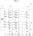
- FIG. 2 is a circuit diagram illustrating an example of a configuration of a plane 300 which may be included in each memory die.
- Each of the first to fourth memory dies DIE 1 to DIE 4 of FIG. 1 may include at least one plane.
- FIG. 2 illustrates one memory block 330 .
- plane 300 may include a plurality of memory blocks in other embodiments.
- memory block 330 may be a representative example of each of the plurality of memory blocks.
- the plane 300 may include a voltage supply 310 , a read/write circuit 320 and a memory block 330 .
- the memory block 330 may include a plurality of cell strings 340 coupled to a plurality of corresponding bit lines BL 0 to BLm ⁇ 1.
- the cell string 340 of each column may include one or more drain select transistors DST and one or more source select transistors SST.
- a plurality of memory cells or memory cell transistors MC 0 to MCn ⁇ 1 may be coupled in series between the drain and source select transistors DST and SST.
- each of the memory cells MC 0 to MCn ⁇ 1 may be embodied by an MLC capable of storing data information of a plurality of bits.
- Each of the cell strings 340 may be electrically coupled to a corresponding bit line among the plurality of bit lines BL 0 to BLm ⁇ 1.
- the first cell string is coupled to the first bit line BL 0 and the last cell string is coupled to the last bit line BLm ⁇ 1.
- ‘DSL’ denotes a drain select line
- SSL denotes a source select line
- CSL’ denotes a common source line.
- FIG. 2 illustrates NAND flash memory cells, but a different type of memory cell may be used in other embodiments.
- the memory cells may be NOR flash memory cells or hybrid flash memory cells including two or more types of memory cells combined therein.
- the memory device 150 including plane 300 may be a flash memory device including a conductive floating gate as a charge storage layer or a charge trap flash (CTF) memory device including an insulation layer as a charge storage layer.
- CTF charge trap flash
- the plane 300 may further include a voltage supply 310 which provides voltages (e.g., a program voltage, a read voltage and a pass voltage) to the word lines, for example, according to operation mode.
- the voltage generation operation of the voltage supply 310 may be controlled by a control circuit. Under the control of the control circuit, the voltage supply 310 may select one of the memory blocks (or sectors) of the memory cell array, may select one of the word lines of the selected memory block, and may provide the word line voltages to the selected word line and the unselected word lines as may be needed.
- the plane 300 may include a read and write (read/write) circuit 320 controlled by the control circuit.
- the read/write circuit 320 may operate as a sense amplifier for reading data from the memory cell array.
- the read/write circuit 320 may operate as a write driver for driving bit lines according to data to be stored in the memory cell array.
- the read/write circuit 320 may receive from a buffer data to be stored in the memory cell array and may drive bit lines according to the received data.
- the read/write circuit 320 may include a plurality of page buffers 322 to 326 respectively corresponding to columns (or bit lines) or column pairs (or bit line pairs). Each of the page buffers 322 to 326 may include a plurality of latches.
- the memory cells of the memory block 330 may be coupled to a plurality of word lines WL 0 to WLn ⁇ 1. Memory cells coupled to one word line may be referred to as a physical page.
- FIG. 2 illustrates a physical page 350 including memory cells MC 1 which are coupled to the word line WL 1 . Memory cells may be accessed by the unit of page by the voltage supply 310 and the read/write circuit 320 .
- One memory die may sequentially receive commands, from a channel, for a plurality of planes.
- the plurality of planes which receive the commands may simultaneously perform command operations, each using a voltage supply and a read/write circuit.
- Memory cells may be referred to as a single level cell (SLC) or a multi-level cell (MLC) depending on the number of bits which can be stored in one memory cell.
- a multi-level cell refers to a memory cell which, as one memory cell, can store data having at least two bits.
- the multi-level cell may include a triple-level cell (TLC) or a quadruple-level cell (QLC).
- FIG. 3 is a graph illustrating an embodiment of a threshold voltage distribution of triple-level cells as an example of multi-level cells.
- any one of 2 3 (e.g., eight) threshold voltage distributions may be formed in the memory cell. Due to fine differences in electrical characteristics between a plurality of memory cells, the threshold voltages of memory cells programmed with the same data may form a certain range of a threshold voltage distribution.
- eight threshold voltage distributions P 1 to P 8 may be formed. The eight threshold voltage distributions P 1 to P 8 may represent logic states that are different from one another.
- a first threshold voltage distribution P 1 of the eight threshold voltage distributions P 1 to P 8 may represent an erased state with a logic state of ‘111.’
- Three bits programmed in a triple-level cell may be referred to as a most significant bit (MSB), a central significant bit (CSB) and a least significant bit (LSB), respectively.
- MSB most significant bit
- CSB central significant bit
- LSB least significant bit
- the eight threshold voltage distributions P 1 to P 8 of the memory cells may be formed, for example, through a single program operation.
- voltage supply 310 may perform a program operation and a verify pulse application operation.
- the program operation may include repeatedly performing a program pulse application operation for migrating threshold voltage distributions of the memory cells.
- the verify pulse application operation may include verifying whether threshold voltages of the memory cells correspond to threshold voltage distributions that correspond to data to be programmed. Through these operations, the eight threshold voltage distributions P 1 to P 8 of the memory cells may be formed.
- a program operation for forming, at once, a plurality of threshold voltage distributions corresponding to three bits may be referred to as a one-shot program operation.
- a memory cell may be turned on when a read voltage (e.g., having a level higher than its threshold voltage) is applied, and may be turned off when a read voltage (e.g., having a level lower than its threshold voltage) is applied.
- Data may be read by sensing a current formed in a bit line as the memory cell is turned on or off.
- each of the three bits may be read by applying different read voltages.
- the voltage supply 310 may apply the first and fifth read voltages R 1 and R 5 to read the MSB.
- the program states P 1 , P 6 , P 7 and P 8 in which the MSB has a value of ‘1’ may be distinguished from the program states P 2 to P 5 in which the MSB has a value of ‘0’.
- the voltage supply 310 may apply the second, fourth and sixth read voltages R 2 , R 4 and R 6 to read the CSB, and may apply the third and seventh read voltages R 3 and R 7 to read the LSB.
- the three bits stored in a triple-level cell are not programmed, at once, by a one-shot program operation. In such a case, multiple operations may be performed and the voltage supply 130 may need to identify all the MSB, CSB and LSB by applying the total seven read voltages R 1 to R 7 to read the three bits.
- Each of the triple-level cells in one physical page may include an MSB, a CSB and an LSB.
- MSBs, CSBs, and LSBs of one physical page may be handled as subpages, respectively.
- the subpages in one physical page may be referred to as an MSB page, a CSB page and an LSB page, respectively.
- the controller 130 may interleave commands for a plurality of memory dies and then may provide the interleaved commands to the memory device 150 .
- Interleaving the commands may refer to the case where controller 130 determines a command providing order so that the commands may be sequentially provided to the plurality of memory dies. Since the plurality of memory dies may simultaneously operate based on the interleaved commands, throughput of the memory system 110 may be improved.
- the controller 130 may collect data to be programmed based on a predetermined size, so that a plurality of physical pages may be simultaneously programmed and the data may be arranged in the plurality of physical pages.
- An explanation of how physical pages may be simultaneously programmed in accordance with one embodiment is given with respect to the hierarchical structure of memory device 150 described with reference to FIG. 4 .
- FIG. 4 is a diagram to assist in the explanation of one embodiment of a hierarchical structure of the memory device 150 .
- the hierarchical structure includes a plurality of memory dies DIE 1 to DIE 4 coupled to a plurality of channels CH 1 to CH 4 and a plurality of ways WAY 1 to WAY 4 .
- the plurality of channels CH 1 to CH 4 , the plurality of ways WAY 1 to WAY 4 and the plurality of memory dies DIE 1 to DIE 4 illustrated in FIG. 4 may correspond, for example, to those described with reference to FIG. 1 .
- Each of the plurality of memory dies DIE 1 to DIE 4 may include a plurality of planes. In FIG. 4 , only a plurality of planes PLANE 1 to PLANE 4 in the first memory die DIE 1 are illustrated, and a plurality of planes which may be in the second to fourth memory dies DIE 2 to DIE 4 are not illustrated. Each of the plurality of planes may correspond to plane 300 described with reference to FIG. 2 .
- Each of the plurality of planes may include a plurality of memory blocks BLK 1 , BLK 2 , . . . .
- Each of the plurality of memory blocks BLK 1 , BLK 2 , . . . may include a plurality of physical pages PHY_PAGE.
- one physical page PHY_PAGE may include an MSB page, a CSB page and an LSB page as subpages.
- Memory cells may be erased in units of a memory block and may be accessed in units of physical page.
- One subpage may include one or more clusters CLUSTER.
- the cluster may include a memory region of a smallest unit to be accessed by the host 102 .
- the memory system 110 may be identified and accessed by the unit of 4 KB by the host 102 .
- the host 102 may allocate a logical address to data by the unit of 4 KB.
- one subpage of the memory system 110 is capable of storing data of 8 KB
- two clusters may be included in one subpage. Data which can be stored in one cluster may be referred to, for example, as a data chunk.
- controller 130 may group memory blocks which are simultaneously accessible and may handle the grouped memory blocks as a super block. For example, controller 130 may generate a super block by grouping memory blocks, each of which is one memory block of each plane in the memory device 150 .
- FIG. 4 illustrates an example of a first virtual super block VSBN 1 in which first memory blocks BLK 1 having a same identifier are grouped from all or a predetermined number of planes, and a second virtual super block VSBN 2 in which second memory blocks BLK 2 having a same identifier are grouped.
- the reason why the super blocks illustrated in FIG. 4 are referred to as virtual super blocks is because the super blocks may include virtualized memory blocks.
- the first memory block BLK 1 may indicate a first physical block having a first physical address in a plane, but, when the first physical block is a bad block, may indicate another memory block for replacing the bad block.
- the controller 130 may handle pages which can be simultaneously accessed (among a plurality of physical pages in the super block) as a stripe.
- the controller 130 may control a program operation and a read operation of the memory device 150 in units of a stripe.
- the controller 130 may group physical pages which can be simultaneously accessed from memory dies coupled to different channels, among a plurality of physical pages in the super block.
- FIG. 4 illustrates an example of a stripe 400 in which physical pages are grouped, where each physical page is one physical page of each of the planes in the first to fourth memory dies DIE 1 to DIE 4 coupled to the fourth way WAY 4 .
- the controller 130 may collect data chunks to be written and arrange the data chunks in a plurality of clusters in the stripe.
- the controller 130 may interleave one-shot program type write commands by arranging the data chunks in the plurality of clusters.
- An operation in which controller 130 arranges a plurality of data chunks in the plurality of clusters, so that the data chunks can be programmed in parallel, may be referred to as a striping operation.
- the controller 130 may provide write commands for the stripe to the memory device 150 .
- a physical address may include an upper address and a lower address.
- the upper address may designate a stripe.
- Stripes in the memory device 150 may be identified by super block addresses-word line addresses-way addresses.
- the stripe 400 may be identified by the addresses of VSBN 1 -WL 1 -WAY 4 .
- the lower address may designate clusters in a stripe.
- a plurality of clusters in the stripe may be identified by channel addresses-subpage addresses-plane addresses-cluster addresses.
- the controller 130 may use the lower address to designate a cluster in which each data chunk is to be stored.
- FIGS. 5 A to 5 C are diagrams to assist in the explanation of examples of a striping operation of the controller 130 in accordance with one or more embodiments.
- FIG. 5 A illustrates an example of one-shot-based striping scheme and an interleaving-based striping scheme.
- the throughput of a write operation and the throughput of a read operation of the memory system 110 may vary depending on a scheme in which the controller 130 stripes data chunks.
- one stripe 400 is shown along with a plurality of clusters in the stripe 400 .
- a hatched cluster represents a cluster in which a data chunk is already arranged, and a cluster with no pattern represents a cluster in which no data chunk is arranged.
- the controller 130 may complete the arrangement of data chunks in LSB pages of the first memory die DIE 1 of the stripe 400 , and then may determine clusters in which data chunks to be written next are to be arranged.
- FIG. 5 A illustrates an arrangement 502 of the next data chunks in one-shot-based striping and an arrangement 504 of the next data chunks in die interleaving-based striping.
- a one-shot-based striping scheme may refer to a scheme of striping data chunks so that successive data chunks can be one-shot programmed.
- the controller 130 may start to arrange the next data chunks first in the CSB pages of the first memory die DIE 1 . After completing the arrangement of data chunks in the first memory die DIE 1 , the controller 130 may arrange data chunks sequentially in the second to fourth memory dies DIE 2 to DIE 4 .
- the controller 130 may control a one-shot program operation for the memory die. If the one-shot program operation is completed even before the arrangement of data chunks in the remaining memory dies is completed, the controller 130 may remove written data from a buffer of the controller 130 . Therefore, data to be programmed may occupy a relatively small portion of the buffer. However, in order to read successively programmed data chunks, the memory die to which the data chunks are programmed may perform multiple (e.g., three) read operations for reading the LSB pages, the CSB pages and the MSB pages included therein. Since the other dies are in an idle state, throughput of a read operation may be reduced.
- the memory die to which the data chunks are programmed may perform multiple (e.g., three) read operations for reading the LSB pages, the CSB pages and the MSB pages included therein. Since the other dies are in an idle state, throughput of a read operation may be reduced.
- the interleaving-based striping scheme may include a scheme of striping data chunks so that consecutive data chunks are interleaved over a plurality of dies. For example, the controller 130 may start to arrange the next data chunks first in the LSB pages of the second memory die DIE 2 . After completing the arrangement of data chunks in the LSB pages of all the memory dies of the stripe 400 , the controller 130 may arrange data chunks sequentially in the CSB pages and the MSB pages. In the case where the controller 130 uses the interleaving-based striping scheme, throughput of a read operation may be improved since the plurality of memory dies may simultaneously perform the read operation when successively programmed data are read. However, data to be programmed may occupy a relatively large portion of the buffer.
- the controller 130 may select any one of a plurality of striping schemes depending on the type of data to be written. For example, the controller 130 may perform one-shot-based striping to write host data and may perform interleaving-based striping to write garbage collection data.
- FIG. 5 B is a diagram illustrating an example of whether to skip a certain memory region based on storage of a parity chunk.
- the controller 130 may skip the arrangement of data chunks in some memory regions in a certain stripe.
- the controller 130 may store a parity chunk for data chunks (stored in a plurality of clusters) in another cluster. For example, the controller 130 may perform a chipkill operation of storing a parity chunk in a cluster, which chipkill operation may be initiated by performing a logical (e.g., XOR) operation on a plurality of data chunks.
- a logical e.g., XOR
- the data chunk in which the uncorrectable error has occurred may be recovered by performing a logical (e.g., XOR) operation on the remaining data chunks and the parity chunk.
- the controller 130 may generate a parity chunk of data chunks stored in one or more stripes, and may store the parity chunk in a predetermined region of any one stripe among the stripes.
- the predetermined region may be clusters in the fourth plane PLANE 4 of the fourth memory die DIE 4 among the clusters in the any one stripe.
- FIG. 5 B shows an example of the arrangement of next data chunks after the arrangement of data in the third plane PLANE 3 of the fourth memory die DIE 4 of the stripe 400 is completed.
- the controller 130 may arrange data chunks in the fourth plane PLANE 4 .
- a case where the controller 130 arranges data chunks in the fourth plane PLANE 4 is illustrated as a next data chunk arrangement 522 .
- the controller 130 may skip the fourth plane PLANE 4 and may arrange data chunks in a die or subpage of a next order. A case where the controller 130 skips the fourth plane PLANE 4 is illustrated as a next data chunk arrangement 524 .
- a large amount of calculations are performed in order to allow a controller to arrange each data chunk in a cluster.
- the controller considers all of a cluster in which a previous data chunk is arranged, a striping scheme of the data chunk and whether a parity chunk is to be stored.
- FIG. 5 C is a diagram of an example to assist in the explanation of a data chunk arrangement method according to the aforementioned proposed method.
- the controller may correspond to controller 130 for illustrative purposes only.
- the controller 130 may queue a command for a new data chunk and buffer the data chunk.
- the controller 130 may determine a cluster in which the new data chunk is to be arranged, depending on a cluster in which a previous data chunk is arranged.
- the controller 130 may determine whether the previous data chunk is arranged in a cluster of the fourth memory die DIE 4 .
- the cluster in which the new data chunk is to be arranged may be determined in consideration of a position of the previous data chunk and a striping scheme of the current data chunk (S 546 to S 556 ).
- the cluster in which the new data chunk is to be arranged may be determined in consideration of a position of the previous data chunk, a striping scheme of the current data chunk and whether a parity chunk is to be stored or not (S 558 to S 574 ).
- the controller 130 may determine whether the previous data chunk is arranged in a last cluster of a page included in the fourth plane PLANE 4 .
- the controller 130 may consider, at operation S 550 , whether a striping scheme of the current data chunk is an interleaving-based scheme or a one-shot-based scheme.
- the controller 130 may consider whether the previous data chunk is arranged in a last subpage. Based on the result, the controller 130 may arrange the new data chunk in a next subpage (S 554 ) or arrange the new data chunk in a next memory die (S 556 ).
- the controller 130 may arrange the new data chunk in a cluster or plane next to the previous data chunk.
- the controller 130 may determine whether the previous data chunk is arranged in a last cluster of a page included in the third plane PLANE 3 .
- the controller 130 may determine whether to store a parity chunk in the fourth plane PLANE 4 .
- the controller 130 may arrange the new data chunk in the fourth plane PLANE 4 .
- the controller 130 may consider whether a striping scheme of the current data chunk is an interleaving-based scheme or a one-shot-based scheme.
- the controller 130 may consider whether the previous data chunk is arranged in a last subpage. Based on the result, the controller 130 may arrange the next data chunk in a next subpage (S 568 ), in a next stripe (S 570 ), or in the first memory die DIE 1 (S 574 ).
- the controller 130 may exclude a case where a parity chunk is arranged in the fourth plane PLANE 4 , and may determine a position of the next data chunk by performing operations S 564 to S 574 .
- the controller 130 may arrange the new data chunk in a cluster or plane next to the previous data chunk.
- dummy data needs to be stored in clusters in which data chunks are not arranged and the stripe needs to be programmed to the memory device 150 . This may occur as the controller 130 receives a host flush command, and even when all data chunks are not striped in a stripe. Also, in order to determine a position for storing dummy data, the controller 130 considers all of the arrangement of the previous data chunk, a striping scheme of the current data chunk, and whether a parity chunk is to be stored.
- the controller 130 When a large amount of calculations are performed for the controller 130 to stripe each of data chunks, a time for a write operation of the memory system 110 may increase. Therefore, the controller 130 will perform striping with a small amount of calculations so as to improve the write performance of the memory system 110 .
- the controller 130 may store a lookup table for determining a cluster in which a data chunk is to be arranged, among clusters included in a stripe. For example, the controller 130 may count a queued order of a write command and determine a cluster in which a data chunk corresponding to the write command is to be arranged based on the lookup table and the queued order. Also, in one embodiment, the controller 130 may store a plurality of lookup tables which are different from one another depending, for example, on a striping scheme of a data chunk and whether a parity chunk is to be stored.
- the controller 130 may determine a cluster in which a data chunk is to be arranged by counting only a queued order of a write command. Since the controller 130 need not perform calculations for various cases that vary depending on the address of a cluster in which a previous data chunk is arranged (in order to determine a cluster in which a data chunk is to be arranged), the time for a write operation of the memory system 110 may be decreased.
- FIG. 6 is a diagram illustrating an embodiment of a structure of the controller 130 which may include a host interface (I/F) 132 , a processor 134 , a memory I/F 142 , and a memory 144 all operatively coupled via an internal bus.
- I/F host interface
- processor 134 processor 134
- memory I/F 142 processor 134
- memory 144 all operatively coupled via an internal bus.
- the host I/F 132 may be configured to process a command and data of the host 102 and may communicate with the host 102 through one or more of interface protocols. Examples include universal serial bus (USB), multi-media card (MMC), peripheral component interconnect-express (PCI-e or PCIe), small computer system interface (SCSI), serial-attached SCSI (SAS), serial advanced technology attachment (SATA), parallel advanced technology attachment (PATA), enhanced small disk interface (ESDI) and integrated drive electronics (IDE).
- the host I/F 132 may be driven using instructions (e.g., firmware that may be referred to as a host interface layer (HIL)) in order to exchange data with the host.
- HIL host interface layer
- the memory I/F 142 may serve as a memory/storage interface for interfacing the controller 130 and the memory device 150 , in order to allow the controller 130 to control the memory device 150 in response to a request from the host 102 .
- the memory I/F 142 may generate a control signal for the memory device 150 and process data to be provided to the memory device 150 under the control of the processor 134 .
- the memory I/F 142 may work as an interface (e.g., a NAND flash interface) for processing a command and data between the controller 130 and the memory device 150 .
- memory I/F 142 may support data transfer between the controller 130 and the memory device 150 .
- the memory I/F 142 may be driven through firmware referred to as a flash interface layer (FIL) in order to exchange data with the memory device 150 .
- FIL flash interface layer
- the processor 134 may control overall operations of the memory system 110 by driving instructions (e.g., firmware).
- the firmware may be, for example, a flash translation layer (FTL) 136 .
- the processor 134 may be, for example, a microprocessor or a central processing unit (CPU).
- the processor 134 may drive the FTL 136 and perform a foreground operation corresponding to a request received from the host.
- the processor 134 may control a write operation of the memory device 150 in response to a write request from the host and control a read operation of the memory device 150 in response to a read request from the host.
- the controller 130 may perform a background operation onto the memory device 150 through the processor 134 , e.g., microprocessor or CPU.
- the background operation performed onto the memory device 150 may include a garbage collection (GC) operation, a wear-leveling (WL) operation, a map flush operation, or a bad block management operation.
- the memory 144 may serve as a working memory of the memory system 110 and the controller 130 , and may store data for driving the memory system 110 and the controller 130 .
- the controller 130 may control the memory device 150 to perform read, program and erase operations in response to a request from the host 102 .
- the controller 130 may provide data read from the memory device 150 to the host 102 and store data from the host 102 to the memory device 150 .
- the memory 144 may store data for the controller 130 and the memory device 150 in order to perform these operations.
- the memory 144 may be embodied by a volatile memory, e.g., a static random access memory (SRAM) or dynamic random access memory (DRAM).
- the memory 144 may be within or outside of the controller 130 .
- FIG. 6 exemplifies memory 144 as being within the controller 130 .
- the memory 144 may be embodied by an external volatile memory having a memory interface transferring data between the memory 144 and the controller 130 .
- memory 144 may store a write queue 146 for queuing a write request and striping information 148 for striping the queued write request.
- the striping information 148 may include at least one lookup table which indicates addresses of clusters according to an order of striping data chunks.
- the memory 144 may further include a buffer for buffering data corresponding to the write request.
- a striping engine 138 may arrange a data chunk to be written in a cluster of a stripe.
- the striping engine 138 may refer to the striping information 148 in order to arrange the data chunk in a cluster.
- FIG. 7 is a diagram to assist in the explanation of an embodiment of a method for arranging data chunks in clusters.
- a processor 134 a striping engine 138 and a memory 144 of the controller 130 are shown.
- the processor 134 , the striping engine 138 and the memory 144 may correspond, for example, to those described with reference to FIG. 6 .
- a write command may be queued in a write queue 146 and may include a host write command received from the host 102 and an internal write command which is generated in the controller 130 .
- An example of the internal write command is a GC (garbage collection) write command which may accompany a garbage collection operation of processor 134 .
- FIG. 7 illustrates a host queue HQ and a GC queue GQ in which the host write command and the GC write command are queued, respectively.
- the host interface 132 may slice the write command into a plurality of host write commands depending on the size of data related with the write command, and may queue the sliced host write commands in the host queue HQ.
- Each of the sliced host write commands may be, for example, a write command for one data chunk and may be related with one logical address.
- FIG. 7 illustrates logical addresses LA 1 , LA 2 and LA 3 related with host write commands, respectively, queued in the host queue HQ.
- the processor 134 may queue a GC write command in the GC queue GQ.
- the GC write command may be a write command for one data chunk and may be related with one logical address.
- FIG. 7 illustrates logical addresses LA 11 , LA 12 and LA 13 related with GC write commands, respectively, queued in the GC queue GQ.
- the processor 134 may select a stripe in which host data chunks corresponding to host write commands queued in the host queue HQ are to be stored. In order to determine a cluster of the selected stripe in which a data chunk related with the host write command is to be arranged, the processor 134 may provide to the striping engine 138 information on the queued order in which the host write command is queued in the write queue 146 . The aforementioned determination may be made, for example, depending on an order in which a host write command is queued in the host queue HQ.
- the cluster of the stripe in which the data chunk is to be arranged may be identified by a predetermined (e.g., lower) address of the physical address described with reference to FIG. 4 .
- the striping engine 138 may determine a lower address of the host data chunk based on the queued order information obtained from the processor 134 and then may provide the determined lower address to processor 134 .
- the processor 134 may determine a physical address of the host data chunk based on the lower address and an upper address which designates the determined stripe.
- the cluster of the stripe in which the data chunk is to be arranged may be identified by another address or portion of the physical address that is different from the lower address.
- the processor 134 may determine a stripe in which the GC data chunks are to be stored even in the case where GC data chunks corresponding to GC write commands are queued in the GC queue GQ.
- the processor 134 may obtain a lower address of the GC data chunk by providing queued order information to the striping engine 138 .
- the processor 134 may determine a physical address of the GC data chunk based on the lower address and an upper address which designates the determined stripe.
- the processor 134 may generate map data by mapping the logical address of the data chunk (from the host 102 ) and the determined physical address.
- the processor 134 may update the generated map data to the memory 144 .
- the striping engine 138 may select one of the lookup tables and may determine a lower address of a data chunk by referring to the selected lookup table.
- the processor 134 may provide striping mode information to the striping engine 138 so that the striping engine 138 may select a lookup table. For example, the processor 134 may select a striping mode based on a type of a data chunk to be striped and whether a parity chunk is to be inserted into a stripe.
- the striping engine 138 may select a lookup table based on the striping mode.
- striping engine 138 may be implemented by a dedicated hardware circuit.
- the hardware-based striping engine 138 performs striping of data chunks, it is possible to offload an address mapping operation of the processor 134 .
- the striping engine 138 needs to determine a striping scheme and perform the calculation described with reference to FIG. 5 C based on the determined striping scheme and a lower address of a previously arranged data chunk. Therefore, the amount of power consumption of the memory system 110 may increase.
- the striping engine 138 is implemented by hardware, it is difficult to change a fixed striping policy.
- the striping engine 138 may be implemented by a hardware circuit capable of performing a calculation of selecting any one among a plurality of lookup tables based on striping mode information from the processor 134 , and a calculation of outputting a lower address according to queued order information from the processor 134 by referring to the selected lookup table.
- the striping engine 138 outputs a lower address by referring to a lookup table stored in the memory 144 , the number of logic gates for implementing the striping engine 138 may decrease. Also, the amount of power consumption of the memory system 110 may decrease.
- a striping policy may be changed in a flexible and efficient manner by changing the lookup table(s) stored in the memory 144 .
- FIGS. 8 A to 12 B illustrate embodiments of lookup tables corresponding to various striping modes.
- a striping method may be determined depending on a memory cell level of a stripe, a striping scheme and whether a parity chunk is to be inserted.
- FIGS. 8 A and 8 B illustrate a first striping mode and a first lookup table 800 according to an embodiment.
- FIG. 8 A illustrates orders in which data chunks are arranged in clusters in one stripe 400 in a first striping mode.
- the first striping mode may be selected, for example, when a triple-level cell stripe is striped by the interleaving-based striping scheme and a parity chunk is not inserted into the stripe.
- Successive data chunks may be sequentially arranged in clusters of the stripe 400 which have the same subpage address.
- data chunks When data chunks are arranged in the clusters, data chunks may be arranged in clusters which have a next subpage address. Since a parity chunk is not inserted, data chunks may be arranged up to the fourth plane PLANE 4 of the fourth memory die DIE 4 .
- first to 32nd data chunks may be first arranged in LSB pages
- 33rd to 64th data chunks may be arranged in CSB pages
- 65th to 96th data chunks may be arranged in MSB pages.
- the processor 134 may control the memory die to perform a one-shot program operation for the clusters.
- data chunks may be flushed to the first memory die DIE 1 .
- data chunks may be flushed to the second, third and fourth memory dies DIE 2 , DIE 3 and DIE 4 .
- related write commands may be removed from the write queue 146 .
- FIG. 8 B illustrates the first lookup table 800 corresponding to the first striping mode according to an embodiment.
- the first lookup table 800 represents a lower address according to a queued order of a data chunk in the first striping mode.
- the lower address may be identified by three subpage addresses, four channel addresses, four plane addresses and two cluster addresses.
- a cluster address corresponding to the queued order may increase.
- a plane address may increase.
- a memory die address corresponding to the queued order may increase when the plane address is initialized after reaching a maximum value, and a subpage address corresponding to the queued order may increase when the memory die address is initialized after reaching a maximum value.
- the striping engine 138 may determine a lower address of the data chunk by referring to the first lookup table 800 , and may provide the lower address to the processor 134 .
- the 25th data chunk may be arranged in the first cluster of the LSB page of the first plane PLANE 1 of the fourth memory die DIE 4 .
- the striping engine 138 may notify the processor 134 that the queued order is the last queued order, while providing a lower address, corresponding to the queued order, to the processor 134 .
- the processor 134 may initialize queued orders in response to the notification, and may update an upper address so that data chunks may be arranged in a next stripe.
- a subpage address may be expressed as 2-bit data in the first lookup table 800 .
- FIGS. 9 A and 9 B illustrate a second striping mode and a second lookup table 900 according to an embodiment.
- FIG. 9 A illustrates orders in which data chunks are arranged in clusters in one stripe 400 in the second striping mode.
- the second striping mode may be selected, for example, when a triple-level cell stripe is striped by the interleaving-based striping scheme and a parity chunk is inserted into the stripe.
- the arrangement of data chunks may be skipped in clusters predetermined to insert parity chunks, for example, clusters in the fourth plane PLANE 4 of the fourth memory die DIE 4 .
- Successive data chunks may be arranged in clusters except the predetermined clusters among clusters having the same subpage address.
- first to 30th data chunks may be first arranged in LSB pages, 31st to 60th data chunks may be arranged in CSB pages, and 61st to 90th data chunks may be arranged in MSB pages.
- the processor 134 may generate parity chunks by performing logic calculations on data chunks arranged in the stripe and previously striped data chunks, and may arrange the parity chunks in the fourth plane PLANE 4 of the fourth memory die DIE 4 .
- the processor 134 may generate a parity chunk by performing a logical (e.g., XOR) calculation on data chunks corresponding to first clusters of LSB pages among data chunks in stripes, and may arrange the generated parity chunk in the first cluster of the LSB page of the fourth plane PLANE 4 of the fourth memory die DIE 4 .
- data chunks and parity chunks may be flushed to the fourth memory die DIE 4 .
- FIG. 9 B illustrates the second lookup table 900 corresponding to the second striping mode according to an embodiment.
- the second lookup table 900 represents a lower address according to a queued order of a data chunk in the second striping mode.
- the lower address may be identified by three subpage addresses, four channel addresses, four plane addresses and two cluster addresses.
- a cluster address, a plane address, a memory die address and a subpage address may increase similarly to the first lookup table 800 .
- clusters for storing parity chunks included in the fourth plane PLANE 4 of the fourth memory die DIE 4 , may be skipped.
- FIGS. 10 A and 1013 illustrate a third striping mode and a third lookup table 1000 according to an embodiment.
- FIG. 10 A illustrates orders in which data chunks are arranged in clusters in one stripe 400 in the third striping mode.
- the third striping mode may be selected when, for example, a triple-level cell stripe is striped by the one-shot-based striping scheme and a parity chunk is not inserted into the stripe.
- Successive data chunks may be sequentially arranged in clusters in one memory die, among the clusters of the stripe 400 .
- data chunks When data chunks are arranged in the clusters, data chunks may be arranged in clusters in a next memory die.
- first to 24th data chunks may be first arranged in the first memory die DIE 1 .
- data chunks When the arrangement of the 24th data chunk is completed, data chunks may be flushed to the first memory die DIE 1 .
- 25th to 48th data chunks may be arranged in the second memory die DIE 2
- 49th to 72nd data chunks may be arranged in the third memory die DIE 3
- 73rd to 96th data chunks may be arranged in the fourth memory die DIE 4 .
- data chunks may be flushed to the second, third and fourth memory dies DIE 2 , DIE 3 and DIE 4 .
- related write commands may be removed from the write queue 146 .
- FIG. 10 B illustrates the third lookup table 1000 corresponding to the third striping mode according to an embodiment.
- the third lookup table 1000 represents a lower address according to a queued order of a data chunk in the third striping mode.
- the lower address may be identified by three subpage addresses, four channel addresses, four plane addresses and two cluster addresses.
- a cluster address corresponding to the queued order may increase.
- a plane address may increase.
- a subpage address corresponding to the queued order may increase when the plane address is initialized after reaching a maximum value, and a memory die address corresponding to the queued order may increase when the subpage address is initialized after reaching a maximum value.
- FIGS. 11 A and 11 B illustrate a fourth striping mode and a fourth lookup table 1100 according to an embodiment.
- FIG. 11 A illustrates orders in which data chunks are arranged in clusters in one stripe 400 in the fourth striping mode.
- the fourth striping mode may be selected when, for example, a triple-level cell stripe is striped by the one-shot-based striping scheme and a parity chunk is inserted into the stripe.
- the arrangement of data chunks may be skipped in clusters predetermined to insert parity chunks, e.g., clusters in the fourth plane PLANE 4 of the fourth memory die DIE 4 .
- Successive data chunks may be arranged in clusters except the predetermined clusters among clusters in the same memory die.
- the processor 134 may generate parity chunks by performing logic calculations on data chunks arranged in the stripe and previously striped data chunks, and may arrange the parity chunks in the fourth plane PLANE 4 of the fourth memory die DIE 4 .
- FIG. 11 B illustrates the fourth lookup table 1100 corresponding to the fourth striping mode according to an embodiment.
- the fourth lookup table 1100 represents a lower address according to a queued order of a data chunk in the fourth striping mode.
- the lower address may be identified by three subpage addresses, four channel addresses, four plane addresses and two cluster addresses.
- Lower addresses according to queued orders of the fourth lookup table 1100 may be the same as lower addresses according to queued orders of the first to 90th data chunks of the third lookup table 1000 .
- clusters for storing parity chunks in the fourth lookup table 1100 may be skipped.
- FIGS. 12 A and 12 B illustrate a fifth striping mode and a fifth lookup table 1200 according to an embodiment.
- FIG. 12 A illustrates orders in which data chunks are arranged in clusters in a single-level cell stripe 500 in the fifth striping mode.
- the fifth striping mode may be selected when, for example, striping a single-level cell stripe.
- Successive data chunks may be sequentially arranged in clusters in one memory die.
- data chunks When data chunks are arranged in the clusters, data chunks may be arranged in clusters in a next memory die.
- first to eighth data chunks may be first arranged in the first memory die DIE 1 .
- data chunks may be flushed to the first memory die DIE 1 .
- ninth to sixteenth data chunks may be arranged in the second memory die DIE 2
- seventeenth to 24th data chunks may be arranged in the third memory die DIE 3
- 25th to 32nd data chunks may be arranged in the fourth memory die DIE 4 .
- data chunks may be flushed to the second, third and fourth memory dies DIE 2 , DIE 3 and DIE 4 .
- related write commands may be removed from the write queue 146 .
- FIG. 12 B illustrates the fifth lookup table 1200 corresponding to the fifth striping mode according to an embodiment.
- the fifth lookup table 1200 represents a lower address according to a queued order of a data chunk in the fifth striping mode. Since a single-level cell page may store one-bit data per memory cell, the single-level cell page may be handled as having one subpage.
- the lower address may be identified by one subpage address, four channel addresses, four plane addresses and two cluster addresses.
- a lower address according to a queued order of a data chunk in the fifth lookup table 1200 may correspond to a cluster in which a queued order of the same data chunk is shown in FIG. 12 A .
- a cluster address corresponding to the queued order may increase.
- a plane address may increase.
- a memory die address corresponding to the queued order may increase when the plane address is initialized after reaching a maximum value.
- the striping engine 138 may determine a lower address of the data chunk by referring to a lookup table corresponding to the striping mode and may provide the lower address to the processor 134 .
- the striping engine 138 may notify the processor 134 that the queued order is the last queued order and may provide a lower address corresponding to the queued order to the processor 134 .
- the processor 134 may initialize queued orders in response to the notification and update an upper address so that data chunks may be arranged in a next stripe.
- the first to fifth lookup tables 800 , 900 , 1000 , 1100 and 1200 are not limited to including lower addresses corresponding to all queued orders of data chunks.
- each of lookup tables may include only a lower address corresponding to a queued order of a data chunk corresponding to the first cluster of the first plane PLANE 1 in each subpage of each memory die.
- Lower addresses corresponding to remaining queued orders may be derived by performing an addition calculation from the lower address in the lookup table.
- FIG. 13 shows an embodiment of a method that may be, partially or fully, performed by controller 130 according to a write command.
- the processor 134 may queue a write command with a logical address and may buffer a data chunk, related with the write command, in the memory 144 .
- the write command may be a host write command or a background write command, e.g., a GC write command.
- the processor 134 may determine a memory cell level to which the data chunk is to be programmed and a striping scheme. For example, the processor 134 may determine the memory cell level as a single-level cell when the data chunk corresponds to system data or data requiring reliability or when a program operation is performed in a single-level cell mode. The processor 134 may determine the memory cell level as a multi-level cell in the other cases.
- FIGS. 8 A to 11 B were described above by taking, as an example, a case where the multi-level cell is a triple-level cell, the multi-level cell may be another type different from a triple-level cell in another embodiment.
- the processor 134 may determine the striping scheme as an interleaving-based striping scheme when the data chunk is a host data chunk, and may determine the striping scheme as a one-shot-based striping scheme when the data chunk is a GC data chunk.
- the processor 134 may determine a stripe to which the data chunk is to be programmed based on the memory cell level of the data chunk and the striping scheme. For example, the processor 134 may allocate different open super blocks for a program operation in a single-level cell mode and a program operation in a multi-level cell mode. An open super block as a super block allocated for a current program operation may refer to a super block in which all stripes have not yet been programmed. The processor 134 may allocate different open super blocks for a host data chunk and a GC data chunk.
- the processor 134 may select any one open super block among a plurality of open super blocks and may determine a stripe to which the data chunk is to be programmed, so that stripes of the open super block are sequentially programmed.
- the processor 134 may store current stripe information in memory 144 .
- the current stripe information may indicate to which stripe a data chunk is to be programmed in each open block.
- Whether a parity chunk is to be inserted into the stripe may be determined based on an address of the stripe. For example, the processor 134 may generate parity chunks by performing logic calculations on data chunks stored in a predetermined number of stripes in an open super block. The processor 134 may then program the parity chunks to a predetermined region of a stripe having a last address among the stripes. For example, when the processor 134 generates parity chunks by collecting data chunks of four stripes, the processor 134 may not insert the parity chunks into first to third stripes. The processor 134 may generate parity chunks by performing logic calculations on data chunks included in the first to fourth stripes, and may insert the parity chunks into the fourth plane PLANE 4 of the fourth memory die DIE 4 of the fourth stripe.
- the processor 134 may determine a queued order of the queued write command. For example, processor 134 may count the number of times a command is queued in each of the host queue HQ and the GC queue GQ in the write queue 146 .
- the processor 134 may provide the queued order information and striping mode information to striping engine 138 .
- a striping mode may be determined based on a memory cell level, a striping scheme, and/or whether a parity chunk is to be inserted.
- the striping engine 138 may select any one of a plurality of lookup tables, stored in the memory 144 , based on the striping mode information obtained from the processor 134 .
- Each of the lookup tables may include lower address information of a data chunk according to a queued order of a write command in each striping mode.
- the striping engine 138 may determine a lower address of the data chunk based on the queued order information obtained from the processor 134 and the selected lookup table.
- the striping engine 138 may provide the lower address to the processor 134 .
- the striping engine 138 may notify the processor 134 that the queued order is a last queued order.
- the processor 134 may arrange the data chunk in a cluster based on the lower address obtained from striping engine 138 .
- the processor 134 may arrange the data chunk in a cluster by updating map data between the logical address and a physical address related with the data chunk.
- the processor 134 may determine the physical address of the data chunk based on the address of the current stripe determined at operation S 1306 and the lower address of the data chunk.
- the processor 134 may flush the completed data to the memory device 150 .
- the data having a size corresponding to a one-shot program unit may refer to data chunks or parity chunks which are arranged in clusters in one memory die among clusters in one stripe.
- the processor 134 may flush the completely arranged data by providing a write command to a memory die including the clusters.
- the processor 134 may initialize the number of times a command is queued in the write queue 146 and may change the current stripe to a next stripe.
- FIG. 14 shows an embodiment of a method which may be, partially or fully, performed by the controller 130 according to a flush command.
- the host 102 may provide a flush command to the controller 130 , so that write data provided to the memory system 110 is completely programmed to the memory device 150 .
- the controller 130 may provide, to the memory device 150 , a write command for data chunks buffered in the memory 144 in response to the flush command.
- the controller 130 may add dummy chunks to the data chunks to complete data having a size corresponding to a one-shot program unit.
- the controller 130 may also provide a write command for the completed data to the memory device 150 .
- the processor 134 may receive a flush command from the host 102 and may queue the flush command in the write queue 146 .
- the flush command may be queued in the host queue HQ.
- the processor 134 may determine a memory cell level of a stripe to which dummy chunks should be added and a striping scheme.
- a memory cell level of data chunks buffered in the memory 144 and a striping scheme may be determined in advance by the operation S 1304 of FIG. 13 .
- the processor 134 may determine a memory cell level of a stripe to which dummy chunks should be added and a striping scheme by referring to the memory cell level and the striping scheme determined in advance.
- the processor 134 may determine a stripe to which dummy chunks should be added.
- a stripe to which data chunks buffered in the memory 144 are to be programmed may be determined in advance by operation S 1306 of FIG. 13 .
- the processor 134 may determine the stripe to which dummy chunks should be added by referring to the stripe determined in advance.
- the processor 134 may further determine whether a parity chunk is to be inserted based on an address of the determined stripe.
- the processor 134 may determine an order in which the flush command is queued. For example, the processor 134 may count the number of times a command is queued in the host queue HQ.
- the processor 134 may provide the queued order information and striping mode information to the striping engine 138 .
- the processor 134 may determine a striping mode based on the memory cell level, a striping scheme and/or whether a parity chunk is to be inserted.
- the striping engine 138 may select any one of a plurality of lookup tables stored in the memory 144 based on the striping mode information obtained from the processor 134 .
- the striping engine 138 may determine lower addresses of clusters in which dummy data need to be arranged by referring to the selected lookup table. For example, the striping engine 138 may determine lower addresses corresponding to the queued order obtained from the processor 134 and orders after the queued order.
- the striping engine 138 may provide the lower addresses to the processor 134 .
- the processor 134 may fill the current stripe with dummy data. For example, the processor 134 may arrange a dummy chunk in a cluster of the current stripe in which a data chunk is not arranged by referring to the lower addresses from the striping engine 138 .
- the processor 134 may flush the stripe including the data chunks and the dummy chunks to the memory device 150 .
- the processor 134 may initialize, in the write queue 146 , the number of times a command is queued and may change the current stripe to a next stripe.
- the processor 134 may provide a striping mode and queued orders, related with the data chunks, to the striping engine 138 .
- the striping engine 138 may select a lookup table based on the striping mode, and may determine lower addresses related with the plurality of data chunks by referring to the selected lookup table and the queued orders.
- the processor 134 may stripe the plurality of data chunks by arranging the plurality of data chunks in clusters based on the lower addresses.
- the striping engine 138 may be implemented by a hardware circuit capable of determining lookup tables and performing calculations of selecting lower addresses by referring to the lookup tables.
- the processor 134 may obtain a lower address by providing a queued order related with a data chunk to the striping engine 138 , instead of performing a calculation of determining a lower address of a cluster in which the data chunk is to be arranged, based on a lower address of a cluster in which a data chunk is previously arranged. Therefore, the processor 134 may improve the performance of the memory system 110 by offloading a striping operation by the striping engine 138 .
- the methods, processes, and/or operations described herein may be performed by code or instructions to be executed by a computer, processor, controller, or other signal processing device.
- the computer, processor, controller, or other signal processing device may be those described herein or one in addition to the elements described herein. Because the algorithms that form the basis of the methods (or operations of the computer, processor, controller, or other signal processing device) are described in detail, the code or instructions for implementing the operations of the method embodiments may transform the computer, processor, controller, or other signal processing device into a special-purpose processor for performing the methods herein.
- the controllers, processors, engines, devices, modules, units, interfaces, drivers, generators and other signal generating and signal processing features may include, for example, a memory or other storage device for storing code or instructions to be executed, for example, by a computer, processor, microprocessor, controller, or other signal processing device.
- the computer, processor, microprocessor, controller, or other signal processing device may be those described herein or one in addition to the elements described herein.
- the code or instructions for implementing the operations of the method embodiments may transform the computer, processor, controller, or other signal processing device into a special-purpose processor for performing the methods described herein.
Landscapes
- Engineering & Computer Science (AREA)
- Theoretical Computer Science (AREA)
- Physics & Mathematics (AREA)
- General Engineering & Computer Science (AREA)
- General Physics & Mathematics (AREA)
- Human Computer Interaction (AREA)
- Quality & Reliability (AREA)
- Techniques For Improving Reliability Of Storages (AREA)
Abstract
Description
Claims (23)
Applications Claiming Priority (2)
| Application Number | Priority Date | Filing Date | Title |
|---|---|---|---|
| KR10-2020-0166644 | 2020-12-02 | ||
| KR1020200166644A KR20220077573A (en) | 2020-12-02 | 2020-12-02 | Memory system and operation method thereof |
Publications (2)
| Publication Number | Publication Date |
|---|---|
| US20220171570A1 US20220171570A1 (en) | 2022-06-02 |
| US11650929B2 true US11650929B2 (en) | 2023-05-16 |
Family
ID=81751349
Family Applications (1)
| Application Number | Title | Priority Date | Filing Date |
|---|---|---|---|
| US17/245,307 Active 2041-05-21 US11650929B2 (en) | 2020-12-02 | 2021-04-30 | Memory system and operation method thereof |
Country Status (3)
| Country | Link |
|---|---|
| US (1) | US11650929B2 (en) |
| KR (1) | KR20220077573A (en) |
| CN (1) | CN114579485A (en) |
Families Citing this family (6)
| Publication number | Priority date | Publication date | Assignee | Title |
|---|---|---|---|---|
| KR20220145695A (en) * | 2021-04-22 | 2022-10-31 | 에스케이하이닉스 주식회사 | Controller and operating method thereof |
| US12093564B2 (en) * | 2021-08-19 | 2024-09-17 | Micron Technology, Inc. | Partition command queues for a memory device |
| US11941290B2 (en) * | 2021-09-01 | 2024-03-26 | Micron Technology, Inc. | Managing distribution of page addresses and partition numbers in a memory sub-system |
| JP2024044868A (en) * | 2022-09-21 | 2024-04-02 | キオクシア株式会社 | Memory systems, methods, and control circuits |
| CN118708126B (en) * | 2024-08-28 | 2025-01-03 | 山东云海国创云计算装备产业创新中心有限公司 | Data processing method, device, equipment, medium and product based on solid state disk |
| CN121050661A (en) * | 2025-10-31 | 2025-12-02 | 苏州元脑智能科技有限公司 | Read/write request access methods and electronic devices |
Citations (5)
| Publication number | Priority date | Publication date | Assignee | Title |
|---|---|---|---|---|
| US20160019160A1 (en) * | 2014-07-17 | 2016-01-21 | Sandisk Enterprise Ip Llc | Methods and Systems for Scalable and Distributed Address Mapping Using Non-Volatile Memory Modules |
| US20160364181A1 (en) * | 2015-06-10 | 2016-12-15 | Micron Technology, Inc. | Stripe mapping in memory |
| US20190369908A1 (en) * | 2018-06-05 | 2019-12-05 | SK Hynix Inc. | Memory system and operating mehtod thereof |
| KR20200059936A (en) | 2018-11-22 | 2020-05-29 | 에스케이하이닉스 주식회사 | Memory system and operation method thereof |
| US10810123B1 (en) * | 2017-10-25 | 2020-10-20 | EMC IP Holding Company, LLC | Flush strategy for using DRAM as cache media system and method |
-
2020
- 2020-12-02 KR KR1020200166644A patent/KR20220077573A/en not_active Withdrawn
-
2021
- 2021-04-30 US US17/245,307 patent/US11650929B2/en active Active
- 2021-07-12 CN CN202110782181.8A patent/CN114579485A/en not_active Withdrawn
Patent Citations (5)
| Publication number | Priority date | Publication date | Assignee | Title |
|---|---|---|---|---|
| US20160019160A1 (en) * | 2014-07-17 | 2016-01-21 | Sandisk Enterprise Ip Llc | Methods and Systems for Scalable and Distributed Address Mapping Using Non-Volatile Memory Modules |
| US20160364181A1 (en) * | 2015-06-10 | 2016-12-15 | Micron Technology, Inc. | Stripe mapping in memory |
| US10810123B1 (en) * | 2017-10-25 | 2020-10-20 | EMC IP Holding Company, LLC | Flush strategy for using DRAM as cache media system and method |
| US20190369908A1 (en) * | 2018-06-05 | 2019-12-05 | SK Hynix Inc. | Memory system and operating mehtod thereof |
| KR20200059936A (en) | 2018-11-22 | 2020-05-29 | 에스케이하이닉스 주식회사 | Memory system and operation method thereof |
Non-Patent Citations (2)
| Title |
|---|
| An article titled "Everything You Always Wanted to Know About SDRAM (Memory): But Were Afraid to Ask" published by Rajinder Gill on Aug. 15, 2010 (Year: 2010). * |
| An article titled Everything you need to know about SLC, MLC, & TLC NAND Flash published Jul. 27, 2015 (Year: 2015). * |
Also Published As
| Publication number | Publication date |
|---|---|
| CN114579485A (en) | 2022-06-03 |
| US20220171570A1 (en) | 2022-06-02 |
| KR20220077573A (en) | 2022-06-09 |
Similar Documents
| Publication | Publication Date | Title |
|---|---|---|
| US11226895B2 (en) | Controller and operation method thereof | |
| US11650929B2 (en) | Memory system and operation method thereof | |
| US20200233585A1 (en) | Data relocation in hybrid memory | |
| KR102704776B1 (en) | Controller and operation method thereof | |
| US11249897B2 (en) | Data storage device and operating method thereof | |
| US20150347291A1 (en) | Flash memory based storage system and operating method | |
| CN110275673A (en) | Storage device and method of operating the same | |
| US11537318B2 (en) | Memory system and operating method thereof | |
| US12001709B2 (en) | Storage devices and operating methods of storage controllers | |
| US11526439B2 (en) | Storage device and operating method thereof | |
| CN108027764B (en) | Convertible Leaf Memory Map | |
| US20200097400A1 (en) | Memory system and operating method thereof | |
| US11194708B2 (en) | Data relocation in memory having two portions of data | |
| US12461650B2 (en) | Address translation metadata compression in memory devices | |
| KR20210157544A (en) | Memory system, memory controller, and operating method of memory system | |
| US12045476B2 (en) | Storage devices, storage controllers, and operating methods of storage controllers | |
| US20250252053A1 (en) | Storage device for caching data segment in hash-based data segment cache and operating method of the storage device | |
| US11675537B2 (en) | Controller for performing data input/output operation and memory management operation at the same time and operation method thereof | |
| US20200327069A1 (en) | Data storage device and operation method thereof, controller using the same | |
| US20240338123A1 (en) | Storage device grouping a plurality of zones into zone cluster, system and operating method of the storage device | |
| US20250348423A1 (en) | Memory devices, operation methods thereof, and memory systems | |
| CN111857563A (en) | Data storage device, electronic device including the same, and method of operating the same | |
| US20250094090A1 (en) | Storage device determining memory area to which data is written using write throughput and method of operation | |
| US20230393741A1 (en) | Storage device and electronic system | |
| KR20240143315A (en) | Storage device managing buffer storing l2p mapping unit and operating method of the storage device |
Legal Events
| Date | Code | Title | Description |
|---|---|---|---|
| AS | Assignment |
Owner name: SK HYNIX INC., KOREA, REPUBLIC OF Free format text: ASSIGNMENT OF ASSIGNORS INTEREST;ASSIGNOR:KIM, JU HYUN;REEL/FRAME:056094/0425 Effective date: 20210420 |
|
| FEPP | Fee payment procedure |
Free format text: ENTITY STATUS SET TO UNDISCOUNTED (ORIGINAL EVENT CODE: BIG.); ENTITY STATUS OF PATENT OWNER: LARGE ENTITY |
|
| STPP | Information on status: patent application and granting procedure in general |
Free format text: NON FINAL ACTION MAILED |
|
| STPP | Information on status: patent application and granting procedure in general |
Free format text: RESPONSE TO NON-FINAL OFFICE ACTION ENTERED AND FORWARDED TO EXAMINER |
|
| STCF | Information on status: patent grant |
Free format text: PATENTED CASE |
|
| AS | Assignment |
Owner name: MIMIRIP LLC, TEXAS Free format text: ASSIGNMENT OF ASSIGNORS INTEREST;ASSIGNOR:SK HYNIX INC.;REEL/FRAME:067335/0246 Effective date: 20240311 Owner name: MIMIRIP LLC, TEXAS Free format text: ASSIGNMENT OF ASSIGNOR'S INTEREST;ASSIGNOR:SK HYNIX INC.;REEL/FRAME:067335/0246 Effective date: 20240311 |