US11636176B2 - Interpolation method and apparatus for arithmetic functions - Google Patents
Interpolation method and apparatus for arithmetic functions Download PDFInfo
- Publication number
- US11636176B2 US11636176B2 US17/085,971 US202017085971A US11636176B2 US 11636176 B2 US11636176 B2 US 11636176B2 US 202017085971 A US202017085971 A US 202017085971A US 11636176 B2 US11636176 B2 US 11636176B2
- Authority
- US
- United States
- Prior art keywords
- bit
- operand
- generate
- terms
- circuit
- Prior art date
- Legal status (The legal status is an assumption and is not a legal conclusion. Google has not performed a legal analysis and makes no representation as to the accuracy of the status listed.)
- Active, expires
Links
Images


Classifications
-
- G—PHYSICS
- G06—COMPUTING OR CALCULATING; COUNTING
- G06F—ELECTRIC DIGITAL DATA PROCESSING
- G06F7/00—Methods or arrangements for processing data by operating upon the order or content of the data handled
- G06F7/38—Methods or arrangements for performing computations using exclusively denominational number representation, e.g. using binary, ternary, decimal representation
- G06F7/48—Methods or arrangements for performing computations using exclusively denominational number representation, e.g. using binary, ternary, decimal representation using non-contact-making devices, e.g. tube, solid state device; using unspecified devices
- G06F7/544—Methods or arrangements for performing computations using exclusively denominational number representation, e.g. using binary, ternary, decimal representation using non-contact-making devices, e.g. tube, solid state device; using unspecified devices for evaluating functions by calculation
-
- G—PHYSICS
- G06—COMPUTING OR CALCULATING; COUNTING
- G06F—ELECTRIC DIGITAL DATA PROCESSING
- G06F17/00—Digital computing or data processing equipment or methods, specially adapted for specific functions
- G06F17/10—Complex mathematical operations
- G06F17/17—Function evaluation by approximation methods, e.g. inter- or extrapolation, smoothing, least mean square method
-
- G—PHYSICS
- G06—COMPUTING OR CALCULATING; COUNTING
- G06F—ELECTRIC DIGITAL DATA PROCESSING
- G06F7/00—Methods or arrangements for processing data by operating upon the order or content of the data handled
- G06F7/38—Methods or arrangements for performing computations using exclusively denominational number representation, e.g. using binary, ternary, decimal representation
- G06F7/48—Methods or arrangements for performing computations using exclusively denominational number representation, e.g. using binary, ternary, decimal representation using non-contact-making devices, e.g. tube, solid state device; using unspecified devices
- G06F7/50—Adding; Subtracting
-
- G—PHYSICS
- G06—COMPUTING OR CALCULATING; COUNTING
- G06F—ELECTRIC DIGITAL DATA PROCESSING
- G06F7/00—Methods or arrangements for processing data by operating upon the order or content of the data handled
- G06F7/38—Methods or arrangements for performing computations using exclusively denominational number representation, e.g. using binary, ternary, decimal representation
- G06F7/48—Methods or arrangements for performing computations using exclusively denominational number representation, e.g. using binary, ternary, decimal representation using non-contact-making devices, e.g. tube, solid state device; using unspecified devices
- G06F7/52—Multiplying; Dividing
- G06F7/523—Multiplying only
-
- G—PHYSICS
- G06—COMPUTING OR CALCULATING; COUNTING
- G06F—ELECTRIC DIGITAL DATA PROCESSING
- G06F9/00—Arrangements for program control, e.g. control units
- G06F9/06—Arrangements for program control, e.g. control units using stored programs, i.e. using an internal store of processing equipment to receive or retain programs
- G06F9/30—Arrangements for executing machine instructions, e.g. instruction decode
- G06F9/30003—Arrangements for executing specific machine instructions
- G06F9/30007—Arrangements for executing specific machine instructions to perform operations on data operands
- G06F9/3001—Arithmetic instructions
-
- G—PHYSICS
- G06—COMPUTING OR CALCULATING; COUNTING
- G06F—ELECTRIC DIGITAL DATA PROCESSING
- G06F9/00—Arrangements for program control, e.g. control units
- G06F9/06—Arrangements for program control, e.g. control units using stored programs, i.e. using an internal store of processing equipment to receive or retain programs
- G06F9/30—Arrangements for executing machine instructions, e.g. instruction decode
- G06F9/30003—Arrangements for executing specific machine instructions
- G06F9/30007—Arrangements for executing specific machine instructions to perform operations on data operands
- G06F9/30018—Bit or string instructions
Definitions
- Embodiments described herein relate to switching circuits, and more particularly, to techniques for performing operations using interpolation.
- Modern computer systems may perform a variety of computation-intensive tasks. Such tasks may include speech recognition, image recognition, and the like, which may require numerous computation operations, such as, multiply-and-accumulate operations. Computer systems may perform operations using a variety of techniques.
- Some computer systems may rely on software or program instructions to perform computation operations.
- the software or program instructions may iteratively use arithmetic circuits included in the computer system to implement more complicated computation operations. For example, in some computer systems, a multiplication operation may be performed using successive addition operations.
- dedicated hardware circuits may be employed to perform some computation operations.
- some computer systems may include circuits configured to multiply two operands to generate a product.
- the dedicated hardware circuits may be used in conjunction with software or program instructions to perform more complicated computation operations.
- a plurality of logic circuits may be configured to receive an operand that includes a plurality of bits occupying respective ordered bit positions.
- a particular logic circuit of the plurality of logic circuits may be configured to generate a conditionally negated value of the operand starting at a particular bit position of the ordered bit positions, and generate a corresponding term of one or more terms using the conditionally negated value and a value of a bit occupying the particular one of the ordered bit positions.
- An output circuit may be configured to combine the operand and the plurality of terms to generate an approximation of a result of an arithmetic function performed on the operand.
- the output circuit may be further configured to combine the operand with a weighted sum of the plurality of terms.
- FIG. 1 is a block diagram of an embodiment of an interpolation circuit.
- FIG. 2 is a block diagram of an embodiment of a logic circuit used in an interpolation circuit.
- FIG. 3 is a block diagram of an embodiment of an output circuit used in an interpolation circuit.
- FIG. 4 is a block diagram of an embodiment of a multiplier circuit using a squaring interpolation circuit.
- FIG. 5 A depicts a graph illustrating a non-interpolatory bisection approximation of a function.
- FIG. 5 B depicts a graph illustrating an interpolatory approximation of a function.
- FIG. 6 illustrates a graph depicting a hat function on the interval [0,1].
- FIG. 7 illustrates a graph depicting a composition of functions forming a nodal basis for the hat function.
- FIG. 8 illustrates a graph depicting a hierarchical basis for the hat function.
- FIG. 9 illustrates a graph depicting the combination of a linear ramp and a step function to form a hat function.
- FIG. 10 illustrates a graph depicting two linear ramps over the unit interval.
- FIG. 11 illustrates a graph depicting example waveforms of the function h(h(x)).
- FIG. 12 is a block diagram of another embodiment of an interpolation circuit.
- FIGS. 13 A-C depict a series of graphs illustrating an improvement in accuracy of approximating a function.
- FIG. 14 is a flow diagram depicting an embodiment of a method for operating an interpolation circuit.
- FIG. 15 illustrates a block diagram of a computer system.
- circuits, or other components may be described as “configured to” perform a task or tasks.
- “configured to” is a broad recitation of structure generally meaning “having circuitry that” performs the task or tasks during operation.
- the unit/circuit/component can be configured to perform the task even when the unit/circuit/component is not currently on.
- the circuitry that forms the structure corresponding to “configured to” may include hardware circuits.
- various units/circuits/components may be described as performing a task or tasks, for convenience in the description.
- the term “based on” is used to describe one or more factors that affect a determination. This term does not foreclose the possibility that additional factors may affect the determination. That is, a determination may be solely based on specified factors or based on the specified factors as well as other, unspecified factors.
- a determination may be solely based on specified factors or based on the specified factors as well as other, unspecified factors.
- circuits or algorithms may be employed that approximate the answer to a desired level of accuracy with a savings of implementation cost, circuit size, power dissipation, or delay (speed).
- Circuits that calculate approximate answers may use different techniques in performing the approximation. For example, some circuits employ successive approximation using a binary search or other suitable algorithm. In other cases, a circuit may employ an interpolation technique, which can improve accuracy of a result while not increasing the complexity of the circuit. Some interpolation techniques (e.g., linear piecewise approximation) combine multiple linear ramp functions to generate an approximation of a particular function.
- an organizational principle to implement a logic circuit for approximating certain arithmetic functions can be developed by combining the absolute value function with a binary step function. For example, such a combination produces a function whose terms correspond to an absolute value representation of a signed binary number.
- the embodiments illustrated in the drawings and described below provide techniques for using a logic circuit to perform interpolation to approximate a result of an arithmetic function using a basis that is implemented using the absolute value representation of a signed binary number.
- the absolute value function is an example of a conditional negation in which the negation depends on the sign bit which is the most significant bit. For a two's complement number system, the negated value must be incremented by one.
- interpolation circuit 100 includes logic circuits 101 and output circuit 102 .
- Logic circuits 101 are configured to receive operand 103 that includes a plurality of bits occupying respective ones of ordered bit positions 104 .
- ordered bit positions 104 may start at position 0 and increment by one for each subsequent position.
- the lowest-order bit may be referred to as the “least significant bit,” while the highest-ordered bit may be referred to as the “most significant bit.”
- interpolation circuit 100 may be configured to generate multiple terms that correspond to multiple absolute values of the operand starting at respective bit positions of the operand.
- a particular one of logic circuits 101 is configured to generate an absolute value of a corresponding portion of operand 103 starting at a particular one of ordered bit positions 104 .
- the particular one of logic circuits 101 is also configured to generate a corresponding term of terms 105 using the complemented or negated value and a value of a bit occupying the particular one of the ordered-bit positions. It is noted that although only three circuits are depicted as being included in logic circuits 101 , in other embodiments, any suitable number of logic circuits may be employed. In some cases, the number of logic circuits included in logic circuits 101 may be, at least in part, a function of a desired accuracy of approximation results 106 as well as a number of bits included in operand 103 .
- Output circuit 102 is configured to combine operand 103 and terms 105 to calculate approximation result 106 .
- output circuit 102 may combine terms 105 in any suitable fashion.
- output circuit 102 may combine terms 105 to operand 103 to calculate approximation result 106 .
- approximation result 106 is an approximation of a result of an arithmetic operation performed on operand 103 .
- approximation result 106 may be an approximation of a square of operand 103 .
- the use of the absolute value of operand 103 allows interpolation circuit 100 to generate approximation result 106 with an accuracy to other circuit implementations, while employing less circuitry.
- the absolute value of a signed binary number is a complement of the binary number with respect to 2 N-1 , where Nis a positive integer corresponding to a number of bits included in the binary number.
- the absolute of a signed binary number may be generated by conditionally inverting the logical value of each bit of the binary number and then adding one based on the value of the leading bit position.
- Logic circuits 101 may include any of these suitable topologies to generate the negation of operand 103 .
- FIG. 2 a block diagram illustrating an embodiment of a particular one of logic circuits 101 is depicted. As illustrated, logic circuit 200 includes exclusive-OR gates 201 - 203 , and adder circuits 204 - 206 . Note that although only three exclusive-OR gates and three adder circuits are depicted in the embodiment of FIG. 2 , in other embodiments, any suitable number of exclusive-OR gates and adders circuits may be employed.
- Inputs of exclusive-OR gate 201 couple to operand bit 1 and operand bit 2 of operand 103 .
- inputs of exclusive-OR gate 202 couple to operand bit 1 and operand bit 3 of operand 103
- inputs of exclusive-OR gate 203 couple to operand bit 1 and operand bit n of operand 103 .
- Each of exclusive-OR gates 201 - 203 may be particular embodiments of a combinatorial logic circuit configured to perform the exclusive-OR logic function.
- a given one of exclusive-OR gates 201 - 203 may be implemented as a complex logic gate using multiple metal-oxide semiconductor field-effect transistors (MOSFETs).
- MOSFETs metal-oxide semiconductor field-effect transistors
- gates 201 - 203 may be implemented using any suitable combination of NAND gates, OR gates, or any other suitable logic gate configured to perform the exclusive-OR logic function.
- Inputs of adder circuits 204 - 206 are coupled to respective outputs of exclusive-OR gates 201 - 203 , and the carry-in inputs of adder circuits 204 - 206 are coupled to the carry-out signal (e.g., carry-out signals 211 - 212 ) generated by a proceeding one of adder circuits 204 - 206 .
- the input of adder circuit 204 is coupled to the output of exclusive-OR gate 201
- the carry-in input of adder circuit 204 is coupled to the carry-out of adder circuit 205 .
- one of the inputs of adder circuit 206 is coupled to operand bit 1 in order to convert the given portion of operand 103 into two's complement format.
- Each of adder circuits 204 - 206 may be implemented as single-bit adder circuits configured to add an input bit and a carry-in bit to generate an output bit and a carry-out bit.
- adder circuits 204 - 206 may include any suitable combination of logic gates, MOSFETs, and the like configured to perform the addition operation.
- each of terms 105 generate the two's complement of different portions of operand 103 starting at respective bit positions within operand 103 .
- a second term of terms 105 may be generated starting at bit position two within operand 103 .
- exclusive-OR gate 201 and adder circuit 204 may be omitted, as operand bit 1 would not be used in the second term. Since each subsequent term is generated using the next-higher bit position, each subsequent instance of logic circuit 200 includes less circuitry, thereby decreasing the overall size of logic circuits 101 .
- the approximation may be generated using only the one's complement value.
- adder circuits 204 - 206 may be re-located to a different location that is more convenient, or may be omitted entirely, with some loss of accuracy in the approximation.
- FIG. 3 depicts an embodiment of output circuit 102 .
- output circuit 102 includes shift circuits 301 - 303 and combiner circuit 304 . Although only three shift circuits are depicted in FIG. 3 , in various embodiments, there may be a shift circuit for the operand, along with a shift circuit for each term included in terms 105 .
- shift circuits 301 - 303 may include a chain of flip-flop circuits, in which an output of a particular flip-flop circuit couples to an input of a next flip-flop in the chain. In response to an assertion of a control signal, the chain of flip-flop circuits shifts the bit position of each data bit by one position. Multiple assertions of the control can result in shifting the bit positions by any suitable number. In some embodiments, the shifting could be performed, at least in part, using software or program instructions executing on a controller or general-purpose processor circuit.
- Combiner circuit 304 is configured to combine terms 105 and operand 103 to generate approximation result 106 .
- combiner circuit 304 may be implemented using multiple half-subtractor or full-subtractor circuits, each configured to perform a subtraction operation for each bit of the difference between any of terms 105 and operand 103 .
- Combiner circuit 304 may, in some embodiments, include any suitable combination of logic gates or MOSFETs configured to implement the desired subtraction functionality. It is noted that in other embodiments, combiner circuit 304 may be implemented using an adder circuit to combine terms 105 and operand 103 to generate approximation result 106 .
- the circuits depicted in FIGS. 1 - 3 may be used to calculate the square of a number. While these circuits are certainly useful when the square of a number is needed, having the ability to generate a square a number also allows for performing other computations. For example, as illustrated in Equation 1, the product of two numbers x and y can be determined using a difference between a square of the sum of the two numbers and square of the difference between the two numbers.
- multiplier circuit 400 includes adder circuit 401 , subtractor circuit 402 , interpolations circuit 403 , and subtractor circuit 404 .
- Adder circuit 401 may be a full adder circuit, or any other suitable adder circuit, configured to generate sum 407 using operand 405 and operand 406 .
- operands 405 and 406 may each include any suitable number of bits, and adder circuit 401 may be configured to accommodate the number of bits included in operands 405 and 406 .
- subtractor circuit 402 may be a full subtractor circuit, or any other suitable subtractor circuit, configured to generate difference 408 using operands 405 and 406 .
- subtractor circuit may be further configured to subtract operand 406 from operand 405 to generate difference 408 .
- subtractor circuit 402 may be configured to accommodate the number of bits included in operands 405 and 406 .
- Interpolation circuit 403 may be an embodiment of interpolation circuit 100 as illustrated in FIG. 1 , configured to generate sum squared 409 using sum 407 , and generate difference squared 410 using difference 408 .
- interpolation circuit 403 may include multiple instances of interpolation circuit 100 in order to generate sum squared 409 and difference squared 410 in parallel rather than in a sequential fashion.
- the number of logic circuits included in interpolation circuit 403 may be based, at least in part, on respective desired accuracies of sum squared 409 and difference squared 410 . Further note that the approximation accuracy of the final multiple operation may also be impacted by the number of logic circuits included in interpolation circuit 403 .
- Subtractor circuit 404 may be a full subtractor or other suitable subtractor circuit configured to subtract difference squared 410 from sum squared 409 to generate product 411 , in accordance with Equation 1. In some embodiments, subtractor circuit 404 may be further configured to divide the product 411 by two.
- register circuits may be included on the inputs and the output of multiplier circuit 400 .
- register circuits may be included between the different stages within multiplier circuit 400 .
- register circuits may be included between adder circuit 401 and interpolation circuit 403 , as well as between subtractor circuit 402 and interpolation circuit 403 .
- FIG. 5 A An example of a non-interpolatory bisection binary approach is depicted in FIG. 5 A . As illustrated, at different points over the unit interval, corresponding bisection values match values of the function that is to be approximated. Note that the function depicted in FIG. 5 A is ⁇ square root over (x) ⁇ , but such approximation techniques, e.g., non-interpolatory bisection binary, may be applied to other functions. At other points on the unit interval, however, the bisection values differ from the values. In some cases, an error associated with the bisection values may be as large as 0.25. While the logic circuits used to implement the bisection approach may be of a desired complexity, the resultant approximation value of the function may be undesirable.
- FIG. 5 B an example of an interpolatory approach to approximating the function is depicted.
- the values of the interpolated function are closer to the actual function values than those generated by the binary bisection approach depicted in FIG. 5 A .
- a maximum error associated with interpolated function is 1/16.
- Different circuit techniques may be used to realize the interpolated function depicted in FIG. 5 B .
- One such technique employs the use of the two's complement of an operand for the function.
- an unsigned N-bit binary number x may be represented as a fractional value greater than or equal to zero and strictly less than one.
- the successive approximation of the x 2 function may be realized using linear piecewise approximation based on hat functions. It is noted that the hat function may be referred to under a variety of names, including chapeau, triangle, mirror, or tent.
- an optimal spacing of the breakpoints of the hat function is an equal or uniform spacing over the unit interval.
- the graph depicted in FIG. 7 is an example that uses four breakpoints. Based on the graph depicted in FIG. 7 , it can be shown that f(x) may be approximated using Equation 4.
- Equation 4 is a linear piecewise approximation of a hat function using the nodal basis depicted in FIG. 7 .
- the hat functions depicted in FIG. 8 define a hierarchical basis.
- H 1 , H 2 , and H 3 may be defined in terms of the hierarchical basis functions of FIG. 8 as shown in Equation 5.
- Equation 6 f(x) can be approximated using Equation 6.
- Equation 7 The result of such a generalization is shown in Equation 7, where h k denotes the uniform spacing of 2 k non-overlapping hat functions on the unit interval.
- h 2 (x) is the same as H 1 +H 2 (or h 1 +h 2 ).
- applying the triangle function to another hat function generates two hierarchical triangles (e.g., h 2 and h 3 depicted in FIG. 8 ).
- Applying the hat function again results in four hierarchical triangles.
- the composition of the hat function results in triangles that double with each repeated composition.
- Equation 8 depicts one example.
- a linear piecewise approximation is built using functions that are linear ramps.
- a particular linear ramp that may be used in linear piecewise approximation is the absolute value function.
- digital logic algorithms are built using step functions, i.e., binary decisions or comparisons whose outputs are either a logical-0 value or a logical-1 value.
- a hat function may be computed from a linear ramp function and a binary-step function. An example of such a hat function is depicted in Equation 9A and FIG. 9 .
- h ⁇ ( x ) ⁇ 2 ⁇ x for ⁇ x ⁇ [ 0 , 1 2 ) 1 - 2 ⁇ x for ⁇ x ⁇ [ 1 2 , 1 ) ( 9 ⁇ A )
- Equation 9A can be rewritten as Equation 9B.
- h ⁇ ( x ) ⁇ 2 ⁇ ⁇ " ⁇ [LeftBracketingBar]" 0 - x ⁇ " ⁇ [RightBracketingBar]” for ⁇ x ⁇ 1 2 2 ⁇ ⁇ " ⁇ [LeftBracketingBar]” 1 - x ⁇ " ⁇ [RightBracketingBar]” for ⁇ x ⁇ 1 2 ( 9 ⁇ B )
- Equation 9B may be re-written to express h(x) in terms of the most-significant-bit value of x as shown in Equation 10.
- Equation 11 is the two's complement representation (denoted as TC) of the binary number for x.
- FIG. 11 depicts waveforms of h° 2 (x).
- Equation 11 is the two's complement of x
- Equation 12 corresponds to the two's complement of a portion of the binary number starting with b 2 .
- the operation to generate the two's complement of a number first examines the most-significant-bit, e.g., b 1 , and if the value of b 1 is a logical-0, then no operation is performed. If, however, the value of b 1 is a logical-1, then respective logical values of the bits occupying the bit positions that are less significant are inverted, and a one is added. This may be expressed as shown in Equation 13.
- Equation 13 is not sign extended. As noted above, this can be implemented in a logic circuit by performing shift operations by a power of two, which add little to the complexity of the logic circuit.
- ⁇ y k b k ⁇ ( 0 ⁇ ... ⁇ 0 ⁇ b k + 1 ⁇ b k + 2 ⁇ ... ⁇ b N )
- each additional term in x 2 increases the arithmetic accuracy by a factor of four, which corresponds to two bits of precision per addition or subtraction.
- interpolation circuit 1200 includes hierarchical triangle generator 1201 , nodal transformer 1202 , selection circuit 1203 , weighting network 1204 , and combiner circuit 1205 .
- Hierarchical triangle generator 1201 is configured to generate conditionally negated values 1206 using operand 103 .
- Conditionally negated values 1206 can be used as a nodal basis for the hat function (as depicted in FIG. 7 ).
- hierarchical triangle generator 1201 may be configured to generate multiple terms that correspond to multiple negations values of operand 103 starting at respective bit positions of operand 103 . As depicted below, the multiple negations correspond to different ones of multiple hierarchical triangles associated with the corresponding terms of Equation 15a.
- Hierarchical triangle generator 1201 may be implemented using any suitable set of combinatorial logic gates. In some embodiments, the number of levels may be based on a level of accuracy desired in an approximation of a target function.
- Nodal transformer circuit 1202 is configured to convert the nodal basis formed by negated values 1206 into a different basis to generate terms 1207 .
- the different basis may be mapped directly to the target function (e.g., x 2 ).
- nodal transformer circuit 1202 may be implemented using any suitable combination of combinatorial logic gates.
- Selection circuit 1203 is configured to select particular ones of terms 1207 to generate selected terms 1208 .
- the selection of triangles is based on the target function. For example, for the function x 2 , all of transformed triangles 1207 are employed, so all of terms 1207 are selected. To approximate other functions, particular ones of transformed triangles 1207 may be omitted from selected terms 1208 .
- Selection circuit 1203 may be implemented using any suitable combination of combinatorial logic gates.
- Weighting network 1204 is configured to apply respective weights to selected terms 1208 to generate weighted terms 1209 .
- the value of a given weight is based on the target function to be approximated. In the case of x 2 , the weights are powers of 2 as depicted in Equations 15a and 15b. To approximate other target functions, different weights may be applied to selected terms 1208 .
- the implementation of weighting network 1204 may, in various embodiments, depend on the weights to be applied to selected terms 1208 .
- Combiner circuit 1205 is configured to combine weighted terms 1209 with operand 103 to generate approximation result 1210 .
- combiner circuit 1205 may be further configured to add weighted terms 1209 and operand 103 to generate approximation result 1210 .
- combiner circuit 1205 may be further configured to add 1 to each of weighted terms 1209 to recover accuracy lost by using conditional negation.
- combiner circuit 1205 may be implemented using multiple single-bit adder circuits configured to add an input bit and a carry-in bit to generate an output bit and a carry-out bit.
- interpolation circuit 1200 can be used to approximate addition function besides x 2 .
- interpolation circuit 1200 can be employed to generate approximations of ⁇ square root over (x) ⁇ , sin x, or any other suitable function. It is contemplated that, in some embodiments, selection circuit 1203 and weighting network 1204 may be adjustable such that interpolation circuit 1200 can be used to approximate different functions at different times.
- FIG. 13 A depicts the function x 2 over the unit interval along with the first term of the interpolation function as defined in Equations 15a and 15b (i.e., 1 ⁇ 4 h(x)). While the first term of Equation 15a matches the function x 2 at three points, there is a difference between the function x 2 and the first term over the remaining points of the unit interval.
- FIG. 13 B the difference over the unit interval between the first term of Equation 15 and the function x 2 is plotted along with 1/16 h(h(x)), which is the second term of Equation 15.
- the second term of Equation 15 has two triangles, which match the residue generated by subtracting the first term from the function x 2 .
- the difference between the residue and the second term is less than the difference depicted in FIG. 13 A .
- Equation 15 The effect of the inclusion of the next term of Equation 15 is depicted in FIG. 13 C . As illustrated, the difference between the function x 2 and 1/16 h(h(x)) is plotted along 1/64 h(h(h(x))).
- the third term of Equation 15 includes four triangles, which match the residue generated by subtracting the second term of Equation 15 from the function x 2 .
- FIG. 14 a flow diagram depicting an embodiment of a method for operating an interpolator circuit is illustrated.
- the method which may be applied to interpolator circuit 100 , begins at block 1401 .
- the method includes receiving data indicative of an arithmetic operation and an operand that includes a plurality of bits occupying respective ones of a plurality of ordered bit positions (block 1402 ).
- the arithmetic operation includes a squaring function or a sine function.
- the method also includes generating a plurality of negated values of respective portions of the operand starting at corresponding bit positions of the plurality of ordered bit positions (block 1403 ).
- generating the plurality of negated values includes performing a plurality of exclusive-OR operations using a bit value at a particular bit position of the ordered bit positions and respective ones of the remaining set of bits of the plurality of bits to generate a plurality of results, and adding the bit value at the particular bit position and a sum of the plurality of result bits.
- the remaining set of bits occupy bit positions of the plurality of ordered bit positions that are less significant than the particular bit position.
- the method further includes combining the operand and the plurality of conditionally negated values to generate an approximation of a result of the arithmetic operation performed on the operand (block 1404 ).
- a number of negated values included in the plurality of negated values is based on a particular accuracy associated with the approximation.
- combining the operand and the plurality of negated values includes subtracting the plurality of negated values from the operand.
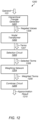
- computer system 1500 includes analog/mixed-signal circuits 1501 , processor circuit 1502 , memory circuit 1503 , and input/output circuits 1504 , each of which is coupled to communication bus 1505 .
- computer system 1500 may be a system-on-a-chip (SoC) and/or be configured for use in a desktop computer, server, or in a mobile computing application such as, e.g., a tablet, laptop computer, or wearable computing device.
- SoC system-on-a-chip
- Analog/mixed-signal circuits 1501 may include a crystal oscillator circuit, a phase-locked loop circuit, an analog-to-digital converter (ADC) circuit, and a digital-to-analog converter (DAC) circuit (all not shown). In other embodiments, analog/mixed-signal circuits 1501 may be configured to perform power management tasks with the inclusion of on-chip power supplies and voltage regulators.
- ADC analog-to-digital converter
- DAC digital-to-analog converter
- Processor circuit 1502 may, in various embodiments, be representative of a general-purpose processor that performs computational operations.
- processor circuit 1602 may be a central processing unit (CPU) such as a microprocessor, a microcontroller, an application-specific integrated circuit (ASIC), or a field-programmable gate array (FPGA).
- processor circuit 1502 is coupled to interpolation circuit 100 or multiplier circuit 400 .
- interpolation circuit 100 and multiplier circuit 400 are depicted as being directly coupled to processor circuit 1502 , in other embodiments, processor circuit 1502 may communicate with interpolation circuit 100 or multiplier circuit 400 via communication bus 1505 or any other suitable communication mechanism.
- Memory circuit 1503 may in various embodiments, include any suitable type of memory such as a Dynamic Random-Access Memory (DRAM), a Static Random-Access Memory (SRAM), a Read-Only Memory (ROM), Electrically Erasable Programmable Read-only Memory (EEPROM), or a non-volatile memory, for example. It is noted that although a single memory circuit is illustrated in FIG. 15 , in other embodiments, any suitable number of memory circuits may be employed.
- DRAM Dynamic Random-Access Memory
- SRAM Static Random-Access Memory
- ROM Read-Only Memory
- EEPROM Electrically Erasable Programmable Read-only Memory
- Input/output circuits 1504 may be configured to coordinate data transfer between computer system 1500 and one or more peripheral devices.
- peripheral devices may include, without limitation, storage devices (e.g., magnetic or optical media-based storage devices including hard drives, tape drives, CD drives, DVD drives, etc.), audio processing subsystems, or any other suitable type of peripheral devices.
- input/output circuits 1504 may be configured to implement a version of Universal Serial Bus (USB) protocol or IEEE 1394 (Firewire®) protocol.
- Input/output circuits 1504 may also be configured to coordinate data transfer between computer system 1500 and one or more devices (e.g., other computing systems or integrated circuits) coupled to computer system 1500 via a network.
- input/output circuits 1504 may be configured to perform the data processing necessary to implement an Ethernet (IEEE 802.3) networking standard such as Gigabit Ethernet or 10-Gigabit Ethernet, for example, although it is contemplated that any suitable networking standard may be implemented.
- Ethernet IEEE 802.3
- input/output circuits 1504 may be configured to implement multiple discrete network interface ports.
Landscapes
- Engineering & Computer Science (AREA)
- Physics & Mathematics (AREA)
- General Physics & Mathematics (AREA)
- Theoretical Computer Science (AREA)
- Mathematical Analysis (AREA)
- Pure & Applied Mathematics (AREA)
- Computational Mathematics (AREA)
- Mathematical Optimization (AREA)
- General Engineering & Computer Science (AREA)
- Software Systems (AREA)
- Data Mining & Analysis (AREA)
- Mathematical Physics (AREA)
- Computing Systems (AREA)
- Algebra (AREA)
- Databases & Information Systems (AREA)
- Complex Calculations (AREA)
Abstract
Description
f(x)=x(1−x) (3)
A graphical depiction of a hat function is illustrated in
from x yields two linear ramps over the intervals
respectively. The two linear ramps are illustrated in
from each of these ramps, then taking the absolute value and multiplying by four, results in the function h°2(x).
Claims (15)
Priority Applications (1)
| Application Number | Priority Date | Filing Date | Title |
|---|---|---|---|
| US17/085,971 US11636176B2 (en) | 2020-09-25 | 2020-10-30 | Interpolation method and apparatus for arithmetic functions |
Applications Claiming Priority (2)
| Application Number | Priority Date | Filing Date | Title |
|---|---|---|---|
| US202063083370P | 2020-09-25 | 2020-09-25 | |
| US17/085,971 US11636176B2 (en) | 2020-09-25 | 2020-10-30 | Interpolation method and apparatus for arithmetic functions |
Publications (2)
| Publication Number | Publication Date |
|---|---|
| US20220100818A1 US20220100818A1 (en) | 2022-03-31 |
| US11636176B2 true US11636176B2 (en) | 2023-04-25 |
Family
ID=80821321
Family Applications (1)
| Application Number | Title | Priority Date | Filing Date |
|---|---|---|---|
| US17/085,971 Active 2041-05-29 US11636176B2 (en) | 2020-09-25 | 2020-10-30 | Interpolation method and apparatus for arithmetic functions |
Country Status (1)
| Country | Link |
|---|---|
| US (1) | US11636176B2 (en) |
Citations (7)
| Publication number | Priority date | Publication date | Assignee | Title |
|---|---|---|---|---|
| US2890829A (en) * | 1956-10-08 | 1959-06-16 | Sperry Rand Corp | Logical binary powering circuits |
| US3780278A (en) * | 1971-03-10 | 1973-12-18 | Du Pont | Binary squaring circuit |
| US20030016822A1 (en) * | 2001-03-06 | 2003-01-23 | Dent Paul W. | Recursive cryptoaccelerator and recursive VHDL design of logic circuits |
| US6748410B1 (en) | 1997-05-04 | 2004-06-08 | M-Systems Flash Disk Pioneers, Ltd. | Apparatus and method for modular multiplication and exponentiation based on montgomery multiplication |
| US8190669B1 (en) | 2004-10-20 | 2012-05-29 | Nvidia Corporation | Multipurpose arithmetic functional unit |
| US20170293471A1 (en) * | 2014-03-28 | 2017-10-12 | Universidad De Málaga | Arithmetic units and related converters |
| US9916131B2 (en) | 2013-10-02 | 2018-03-13 | The Penn State Research Foundation | Techniques and devices for performing arithmetic |
-
2020
- 2020-10-30 US US17/085,971 patent/US11636176B2/en active Active
Patent Citations (7)
| Publication number | Priority date | Publication date | Assignee | Title |
|---|---|---|---|---|
| US2890829A (en) * | 1956-10-08 | 1959-06-16 | Sperry Rand Corp | Logical binary powering circuits |
| US3780278A (en) * | 1971-03-10 | 1973-12-18 | Du Pont | Binary squaring circuit |
| US6748410B1 (en) | 1997-05-04 | 2004-06-08 | M-Systems Flash Disk Pioneers, Ltd. | Apparatus and method for modular multiplication and exponentiation based on montgomery multiplication |
| US20030016822A1 (en) * | 2001-03-06 | 2003-01-23 | Dent Paul W. | Recursive cryptoaccelerator and recursive VHDL design of logic circuits |
| US8190669B1 (en) | 2004-10-20 | 2012-05-29 | Nvidia Corporation | Multipurpose arithmetic functional unit |
| US9916131B2 (en) | 2013-10-02 | 2018-03-13 | The Penn State Research Foundation | Techniques and devices for performing arithmetic |
| US20170293471A1 (en) * | 2014-03-28 | 2017-10-12 | Universidad De Málaga | Arithmetic units and related converters |
Also Published As
| Publication number | Publication date |
|---|---|
| US20220100818A1 (en) | 2022-03-31 |
Similar Documents
| Publication | Publication Date | Title |
|---|---|---|
| Stine et al. | The symmetric table addition method for accurate function approximation | |
| Antelo et al. | High performance rotation architectures based on the radix-4 CORDIC algorithm | |
| Kota et al. | Numerical accuracy and hardware tradeoffs for CORDIC arithmetic for special-purpose processors | |
| CN112119407B (en) | Low-precision deep neural networks enabled by compensation instructions | |
| US20060059215A1 (en) | Cordic unit | |
| TWI800979B (en) | Neural network processing unit and system | |
| Naresh et al. | Design of 8-bit Dadda multiplier using gate level approximate 4: 2 compressor | |
| Fu et al. | A high-speed processor for digital sine/cosine generation and angle rotation | |
| US11636176B2 (en) | Interpolation method and apparatus for arithmetic functions | |
| Villalba et al. | Parallel compensation of scale factor for the CORDIC algorithm | |
| Poczekajlo et al. | Evaluation of new CORDIC algorithms implemented on FPGA for the Givens Rotator | |
| Meyer-Bäse et al. | A parallel CORDIC architecture dedicated to compute the Gaussian potential function in neural networks | |
| Thiruvengadam et al. | Low power approximate adder based repetitive iteration cord (LP-ARICO) algorithm for high-speed applications | |
| Li et al. | Hardware-Efficient Activation Circuit for Edge Computing: Shifter-Polynomial Approximation of Leaky ReLU | |
| Tiwari et al. | Implementation of a fast hybrid CORDIC architecture | |
| Hormigo et al. | CORDIC processor for variable-precision interval arithmetic | |
| Prasanna et al. | Efficient Square Root Computation–An Analysis | |
| Schwarzbacher13 et al. | Optimisation and implementation of the arctan function for the power domain | |
| Saha et al. | High speed multiplier using high accuracy floating point logarithmic number system | |
| Choudhary et al. | Comparative Analysis of Two Hardware-Based Square Root Computational Algorithms | |
| Jain et al. | A new approach for high performance and efficient design of CORDIC processor | |
| Poczekajlo et al. | Low Latency Recoding CORDIC Algorithm for FPGA Implementation | |
| Li et al. | An Area-Power-Efficient Multiplier-less Processing Element Design for CNN Accelerators | |
| Dai et al. | Efficient Floating-Point Divider based on Hybrid Cubic-Quadratic Goldschmidt Algorithm | |
| Hao et al. | A VLSI implementation of double precision floating-point logarithmic function |
Legal Events
| Date | Code | Title | Description |
|---|---|---|---|
| AS | Assignment |
Owner name: APPLE INC., CALIFORNIA Free format text: ASSIGNMENT OF ASSIGNORS INTEREST;ASSIGNORS:ATHAS, WILLIAM C.;NADEEM, ZAID M.;PARSHAKOVA, TETIANA;SIGNING DATES FROM 20201029 TO 20201030;REEL/FRAME:054229/0040 |
|
| FEPP | Fee payment procedure |
Free format text: ENTITY STATUS SET TO UNDISCOUNTED (ORIGINAL EVENT CODE: BIG.); ENTITY STATUS OF PATENT OWNER: LARGE ENTITY |
|
| STPP | Information on status: patent application and granting procedure in general |
Free format text: DOCKETED NEW CASE - READY FOR EXAMINATION |
|
| STPP | Information on status: patent application and granting procedure in general |
Free format text: PRE-INTERVIEW COMMUNICATION MAILED |
|
| STPP | Information on status: patent application and granting procedure in general |
Free format text: NON FINAL ACTION MAILED |
|
| STPP | Information on status: patent application and granting procedure in general |
Free format text: RESPONSE TO NON-FINAL OFFICE ACTION ENTERED AND FORWARDED TO EXAMINER |
|
| STPP | Information on status: patent application and granting procedure in general |
Free format text: NOTICE OF ALLOWANCE MAILED -- APPLICATION RECEIVED IN OFFICE OF PUBLICATIONS |
|
| STCF | Information on status: patent grant |
Free format text: PATENTED CASE |