US11626441B2 - Optical module - Google Patents
Optical module Download PDFInfo
- Publication number
- US11626441B2 US11626441B2 US16/745,139 US202016745139A US11626441B2 US 11626441 B2 US11626441 B2 US 11626441B2 US 202016745139 A US202016745139 A US 202016745139A US 11626441 B2 US11626441 B2 US 11626441B2
- Authority
- US
- United States
- Prior art keywords
- apertures
- pixels
- lens array
- micro lens
- group
- Prior art date
- Legal status (The legal status is an assumption and is not a legal conclusion. Google has not performed a legal analysis and makes no representation as to the accuracy of the status listed.)
- Active, expires
Links
Images


Classifications
-
- H01L27/14627—
-
- G—PHYSICS
- G02—OPTICS
- G02B—OPTICAL ELEMENTS, SYSTEMS OR APPARATUS
- G02B19/00—Condensers, e.g. light collectors or similar non-imaging optics
- G02B19/0033—Condensers, e.g. light collectors or similar non-imaging optics characterised by the use
- G02B19/0076—Condensers, e.g. light collectors or similar non-imaging optics characterised by the use for use with a detector
-
- G—PHYSICS
- G02—OPTICS
- G02B—OPTICAL ELEMENTS, SYSTEMS OR APPARATUS
- G02B3/00—Simple or compound lenses
- G02B3/0006—Arrays
- G02B3/0037—Arrays characterized by the distribution or form of lenses
- G02B3/0056—Arrays characterized by the distribution or form of lenses arranged along two different directions in a plane, e.g. honeycomb arrangement of lenses
-
- H01L27/14623—
-
- H—ELECTRICITY
- H10—SEMICONDUCTOR DEVICES; ELECTRIC SOLID-STATE DEVICES NOT OTHERWISE PROVIDED FOR
- H10F—INORGANIC SEMICONDUCTOR DEVICES SENSITIVE TO INFRARED RADIATION, LIGHT, ELECTROMAGNETIC RADIATION OF SHORTER WAVELENGTH OR CORPUSCULAR RADIATION
- H10F39/00—Integrated devices, or assemblies of multiple devices, comprising at least one element covered by group H10F30/00, e.g. radiation detectors comprising photodiode arrays
- H10F39/10—Integrated devices
- H10F39/12—Image sensors
- H10F39/18—Complementary metal-oxide-semiconductor [CMOS] image sensors; Photodiode array image sensors
-
- H—ELECTRICITY
- H10—SEMICONDUCTOR DEVICES; ELECTRIC SOLID-STATE DEVICES NOT OTHERWISE PROVIDED FOR
- H10F—INORGANIC SEMICONDUCTOR DEVICES SENSITIVE TO INFRARED RADIATION, LIGHT, ELECTROMAGNETIC RADIATION OF SHORTER WAVELENGTH OR CORPUSCULAR RADIATION
- H10F39/00—Integrated devices, or assemblies of multiple devices, comprising at least one element covered by group H10F30/00, e.g. radiation detectors comprising photodiode arrays
- H10F39/80—Constructional details of image sensors
- H10F39/805—Coatings
- H10F39/8057—Optical shielding
-
- H—ELECTRICITY
- H10—SEMICONDUCTOR DEVICES; ELECTRIC SOLID-STATE DEVICES NOT OTHERWISE PROVIDED FOR
- H10F—INORGANIC SEMICONDUCTOR DEVICES SENSITIVE TO INFRARED RADIATION, LIGHT, ELECTROMAGNETIC RADIATION OF SHORTER WAVELENGTH OR CORPUSCULAR RADIATION
- H10F39/00—Integrated devices, or assemblies of multiple devices, comprising at least one element covered by group H10F30/00, e.g. radiation detectors comprising photodiode arrays
- H10F39/80—Constructional details of image sensors
- H10F39/806—Optical elements or arrangements associated with the image sensors
- H10F39/8063—Microlenses
Definitions
- the present disclosure relates to an optical module, and to an optical module including an image sensor and micro lens array.
- An optical module can include an optical structure arranged on a complementary metal-oxide-semiconductor (CMOS) image sensor (CIS) to receive or collect optical information (e.g. fingerprint image).
- CMOS complementary metal-oxide-semiconductor
- CIS complementary metal-oxide-semiconductor image sensor
- the received optical information may include some unwanted signals (or noises, interferences, etc.) which may adversely affect detection of the object.
- an optical module includes an image sensor and micro lens array.
- the image sensor has at least one group of pixels.
- the micro lens array is disposed on the image sensor.
- the at least one group of pixels is shifted from the micro lens array in a first direction from a top view perspective.
- an optical module includes an image sensor and a micro lens array.
- the image sensor has at least one group of pixels.
- the micro lens array is disposed on the image sensor. A projection of one of the micro lens array falls on at least two of the at least one group of pixels.
- an optical module includes an image sensor and a micro lens array and an opaque layer.
- the image sensor has at least one group of pixels.
- the micro lens array is disposed on the image sensor.
- the opaque layer is disposed on the at least one group of pixels ( 80 ) and comprising a plurality of holes.
- a projection area of one lens of the micro lens array is apart from at least one of the plurality of holes.
- FIG. 1 illustrates a cross section of an optical module in accordance with some embodiments of the present disclosure.
- FIG. 2 illustrates a top view of the optical module in accordance with some embodiments of the present disclosure.
- FIG. 3 illustrates a top view of the optical module in accordance with some embodiments of the present disclosure.
- FIG. 4 illustrates a top view of the optical module in accordance with some embodiments of the present disclosure.
- FIG. 5 A to FIG. 5 C illustrate a top view of the optical module in accordance with some embodiments of the present disclosure.
- FIG. 6 illustrates a top view of the optical module in accordance with some embodiments of the present disclosure.
- FIG. 7 illustrates a top view of the optical module in accordance with some embodiments of the present disclosure.
- FIG. 8 A to FIG. 8 F illustrates a top view of an exploded view of the optical module in accordance with some embodiments of the present disclosure.
- FIG. 9 illustrates a cross section of an optical module in accordance with some embodiments of the present disclosure.
- FIG. 10 illustrates a cross section of an optical module in accordance with some embodiments of the present disclosure.
- FIG. 1 illustrates a cross section of an optical module 1 in accordance with some embodiments of the present disclosure.
- the optical module 1 includes at least one group of pixels 80 , an opaque layer 72 a , a transparent material 13 , an opaque layer 12 , a micro lens array 70 and a coating layer 70 c , 70 c also can be applied on 72 a instead of top side.
- the opaque layer 72 a is disposed on the at least one group of pixels 80 .
- the opaque layer 72 a includes a plurality of holes 72 .
- the opaque layer 12 is disposed between the at least one group of pixels 80 and the micro lens array 70 .
- the transparent material 13 may be a transparent photo resist material 13 .
- the opaque layer 12 includes a plurality of apertures 74 .
- the coating layer 70 c is disposed on the micro lens array 70 .
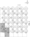
- FIG. 2 illustrates a top view of the optical module 1 in accordance with some embodiments of the present disclosure.
- the at least one group of pixels 80 is shifted from the micro lens array 70 in a first direction from a top view perspective.
- the first direction may be the X direction.
- the at least one group of pixels 80 is shifted from the micro lens array 70 in a second direction from a top view perspective.
- the second direction may be the Y direction.
- the first direction is in perpendicular to the second direction.
- At least one lens of the micro lens array 70 is shifted from a geometrical central axis of one corresponding pixel of the pixels 80 (such as the region III).
- the area of the pixel of the region III is partially covered by a projection of four lenses.
- the at least one aperture 74 is adjacent to the peripheral of one lens of the micro lens array 70 and is shifted from a geometrical central axis of the lens of the micro lens array 70 .
- a projection of one lens of the micro lens array 70 falls on the aperture 74 in the pixel of the region I.
- a projection area of one lens (such as the lens in the region I) of the micro lens array 70 is apart from at least one hole 72 (such as the hole in the region I).
- At least one of the plurality of holes 72 is adjacent to the peripheral of one lens of the micro lens array 70 and is shifted from a geometrical central axis of the lens of the micro lens array 70 . In some embodiments, a projection of one lens of the micro lens array 70 falls one of the plurality of holes 72 in the pixel of the region I. In some embodiments, at least one of the plurality of holes 72 is shifted from one aperture 74 of the opaque layer 12 .
- a projection of one of the micro lens array 70 falls on at least two of the at least one group of pixels 80 . In some embodiments, a projection of one of the micro lens array 70 falls on at least three of the at least one group of pixels 80 . In some embodiments, a projection of one of the micro lens array 70 falls on at least four of the at least one group of pixels 80 .
- an incident light passes through one lens of the micro lens array 70 (such as the lens falls on the regions I and IV), an aperture 74 (such as the aperture falls on the region I) adjacent to the peripheral of the lens of the micro lens array 70 and one of the plurality of holes 72 (such as the a hole falls on the region I) adjacent to the peripheral of the lens of the micro lens array 70 .
- at least one of the plurality of holes 72 is disposed between two adjacent lens of the micro lens array 70 .
- FIG. 3 illustrates a top view of the optical module 1 in accordance with some embodiments of the present disclosure.
- a projection of the aperture 74 of the opaque layer 12 falls on at least two of the at least one group of pixels 80 .
- One of the plurality of holes 72 is disposed between three of the micro lens array 70 .
- a projection of one lens of the micro lens array 70 falls on one aperture 74 .
- a projection of one lens of the micro lens array 70 falls on two apertures 74 . (such as this embodiment, this arrangement can detect the different four directions well, but the utilization of pixels is low)
- FIG. 4 illustrates a top view of the optical module 1 in accordance with some embodiments of the present disclosure.
- a projection of one of the micro lens array 70 falls on at least four of the at least one group of pixels 80 .
- a projection of one lens of the micro lens array 70 falls on three apertures 74 and three different incident lights respectively pass through three different apertures 74 .
- three different incident lights respectively three different holes 72 . (such as this embodiment, this arrangement can detect three different directions only to keep high utilization of pixels)
- FIG. 5 A to FIG. 5 C illustrate a top view of the optical module 1 in accordance with some embodiments of the present disclosure.
- a projection of one lens of the micro lens array 70 falls on two pixels (such as regions I and III).
- a projection of one lens of the micro lens array 70 falls on four pixels (such as regions I, II, III and IV).
- a projection of one lens of the micro lens array 70 falls on one aperture 74 .
- a projection of one lens of the micro lens array 70 falls on two apertures 74 .
- a projection of one lens of the micro lens array 70 falls on three apertures 74 .
- the parameter CP is the minimum length from the hole 72 to the edge of the pixel 80 .
- the parameter R is the radius of one lens of the micro lens array 70 .
- the parameter CL is the length from the hole 72 to the edge of the lens of the micro lens array 70 .
- the parameter P is the length of one edge of the pixel 80 .
- the parameter R is less than or equal to a half of the parameter P.
- a projection of one lens of the micro lens array 70 is contact with the peripheral of the apertures 74 .
- the distance between the geometrical central axis of one lens of the micro lens array 70 and the geometrical central axis of the apertures 74 is larger than the radius of the apertures 74 .
- the peripheral of the apertures 74 is apart from a geometrical central axis of one lens of the micro lens array 70 .
- the geometrical central axis of the apertures 74 is apart from geometrical central axis of one lens of the micro lens array 70 .
- the length of the pixel 80 , the lens of the micro lens array 70 and the related position of the holes 72 are selected in accordance with the following equations.
- CP+CL+R+CP P R ⁇ 2 ⁇ P/ 2
- the parameter R is less than or equal to a half of the parameter P multiplied by ⁇ 2.
- the length of the pixel 80 , the lens of the micro lens array 70 and the related position of the holes 72 are selected in accordance with the following equations. (the second equation below refers to the direction from the pixel regions I to III).
- a projection of one lens of the micro lens array 70 falls in the area of the aperture 74 .
- FIG. 6 illustrates a top view of the optical module 1 in accordance with some embodiments of the present disclosure.
- a projection of one lens of the micro lens array 70 falls on a portion of the four apertures 74 .
- a projection of one lens of the micro lens array 70 falls on a portion of each of four apertures 74 .
- FIG. 7 illustrates a top view of the optical module 1 in accordance with some embodiments of the present disclosure.
- the four regions I to IV of the pixels have two combination designs. A set of the four regions I to IV is aligned with another set of the four regions I to IV. In some embodiments, a set of the four regions I to IV is shifted from another set of the four regions I to IV.
- FIG. 8 A illustrates a top view of an exploded view of the optical module 1 in accordance with some embodiments of the present disclosure.
- the holes 72 are disposed as a line (slash).
- One hole 72 is disposed in one pixel 80 .
- FIG. 8 B illustrates a top view of an exploded view of the optical module 1 in accordance with some embodiments of the present disclosure.
- one aperture 74 is disposed in one pixel 80 .
- a projection of some of the apertures 74 fall on one pixel 80 .
- a projection of some of the apertures 74 fall on two pixels 80 .
- FIG. 8 C illustrates a top view of an exploded view of the optical module 1 in accordance with some embodiments of the present disclosure.
- a projection of one lens of the micro lens array 70 falls on four pixels.
- the pixel is partially covered by a projection of four lenses.
- FIG. 8 D illustrates a top view of an exploded view of the optical module 1 in accordance with some embodiments of the present disclosure.
- a projection of one of the apertures 74 is apart from one hole 72 .
- FIG. 8 E illustrates a top view of an exploded view of the optical module 1 in accordance with some embodiments of the present disclosure.
- a projection of one lens of the micro lens array 70 is apart from one hole 72 .
- FIG. 8 F illustrates a top view of an exploded view of the optical module 1 in accordance with some embodiments of the present disclosure.
- a projection of one lens of the micro lens array 70 falls on one or two apertures 74 .
- a projection of one lens of the micro lens array 70 do not falls on an aperture 74 , such as the lens depicted as the dot line in the pixel region II.
- FIG. 9 illustrates a cross section of an optical module 2 in accordance with some embodiments of the present disclosure.
- the optical module 2 includes an image sensor 10 , an opaque layer 12 , a light path 40 and an illuminated target as finger 60 .
- the image sensor 10 includes at least one group of pixels 80 .
- the image sensor 10 includes a plurality of CISs.
- the image sensor 10 includes at least one group of pixels 80 .
- the micro lens array 70 is disposed on the image sensor 10 .
- the opaque layer 72 a includes a plurality of apertures 74 .
- the light path 40 may be a cone path for receiving the incident light.
- the illuminated light source 50 may be an organic light-emitting diode (OLED).
- OLED organic light-emitting diode
- FIG. 10 illustrates a cross section of an optical module 3 in accordance with some embodiments of the present disclosure.
- the optical module 3 includes an image sensor 10 , an opaque layer 121 and a micro lens array 122 .
- the incident light 901 is illuminated on the micro lens array 122 .
- the incident light 901 passes through the the micro lens array 121 and is refracted.
- the incident light 901 passes through the opaque layer 121 and is illuminated on the image sensor 10 .
- the terms “approximately,” “substantially,” “substantial” and “about” are used to describe and account for small variations. When used in conjunction with an event or circumstance, the terms can refer to instances in which the event or circumstance occurs precisely as well as instances in which the event or circumstance occurs to a close approximation.
- the terms can refer to a range of variation less than or equal to ⁇ 10% of that numerical value, such as less than or equal to ⁇ 5%, less than or equal to ⁇ 4%, less than or equal to ⁇ 3%, less than or equal to ⁇ 2%, less than or equal to ⁇ 1%, less than or equal to ⁇ 0.5%, less than or equal to ⁇ 0.1%, or less than or equal to ⁇ 0.05%.
- two numerical values can be deemed to be “substantially” or “about” the same if a difference between the values is less than or equal to ⁇ 10% of an average of the values, such as less than or equal to ⁇ 5%, less than or equal to ⁇ 4%, less than or equal to ⁇ 3%, less than or equal to ⁇ 2%, less than or equal to ⁇ 1%, less than or equal to ⁇ 0.5%, less than or equal to ⁇ 0.1%, or less than or equal to ⁇ 0.05%.
- a component provided “on” or “over” another component can encompass cases where the former component is directly on (e.g., in physical contact with) the latter component, as well as cases where one or more intervening components are located between the former component and the latter component.
Landscapes
- Physics & Mathematics (AREA)
- General Physics & Mathematics (AREA)
- Optics & Photonics (AREA)
- Transforming Light Signals Into Electric Signals (AREA)
- Optical Elements Other Than Lenses (AREA)
- Lenses (AREA)
- Solid State Image Pick-Up Elements (AREA)
- Studio Devices (AREA)
Abstract
Description
CP+R+CL+CP=P
R≤P/2
CP+CL+R+CP=P
R≤√2×P/2
2R+2CL−P=2CP
P≤2R+2CL≤2P
Claims (9)
Priority Applications (3)
| Application Number | Priority Date | Filing Date | Title |
|---|---|---|---|
| US16/745,139 US11626441B2 (en) | 2020-01-16 | 2020-01-16 | Optical module |
| TW109146607A TWI861329B (en) | 2020-01-16 | 2020-12-29 | Optical module |
| CN202110040025.4A CN113140580A (en) | 2020-01-16 | 2021-01-13 | Optical module |
Applications Claiming Priority (1)
| Application Number | Priority Date | Filing Date | Title |
|---|---|---|---|
| US16/745,139 US11626441B2 (en) | 2020-01-16 | 2020-01-16 | Optical module |
Publications (2)
| Publication Number | Publication Date |
|---|---|
| US20210225917A1 US20210225917A1 (en) | 2021-07-22 |
| US11626441B2 true US11626441B2 (en) | 2023-04-11 |
Family
ID=76810261
Family Applications (1)
| Application Number | Title | Priority Date | Filing Date |
|---|---|---|---|
| US16/745,139 Active 2041-03-14 US11626441B2 (en) | 2020-01-16 | 2020-01-16 | Optical module |
Country Status (3)
| Country | Link |
|---|---|
| US (1) | US11626441B2 (en) |
| CN (1) | CN113140580A (en) |
| TW (1) | TWI861329B (en) |
Families Citing this family (2)
| Publication number | Priority date | Publication date | Assignee | Title |
|---|---|---|---|---|
| US11626441B2 (en) * | 2020-01-16 | 2023-04-11 | Advanced Semiconductor Engineering, Inc. | Optical module |
| WO2024158986A1 (en) * | 2023-01-25 | 2024-08-02 | Meta Platforms Technologies, Llc | Perspective-correct passthrough architectures for head-mounted displays |
Citations (8)
| Publication number | Priority date | Publication date | Assignee | Title |
|---|---|---|---|---|
| US9793308B2 (en) * | 2011-04-22 | 2017-10-17 | Commissariat à l'énergie atomique et aux énergies alternatives | Imager integrated circuit and stereoscopic image capture device |
| US10115753B2 (en) * | 2015-02-16 | 2018-10-30 | Samsung Electronics Co., Ltd. | Image sensor including pixels having plural photoelectric converters configured to convert light of different wavelengths and imaging apparatus including the same |
| CN110473887A (en) | 2018-08-21 | 2019-11-19 | 神盾股份有限公司 | Optical sensor, optical sensor system and its manufacturing method |
| US10627549B2 (en) * | 2015-07-31 | 2020-04-21 | Sony Semiconductor Solutions Corporation | Stacked lens structure, method of manufacturing the same, and electronic apparatus |
| US20200259979A1 (en) * | 2018-10-04 | 2020-08-13 | Samsung Electronics Co., Ltd. | Image sensor and image sensing method |
| US10892289B2 (en) * | 2017-04-17 | 2021-01-12 | Samsung Electronics Co., Ltd. | Optical sensors including a light-impeding pattern |
| US20210225917A1 (en) * | 2020-01-16 | 2021-07-22 | Advanced Semiconductor Engineering, Inc. | Optical module |
| US20210333441A1 (en) * | 2018-07-19 | 2021-10-28 | Isorg | Optical system and process for manufacturing same |
-
2020
- 2020-01-16 US US16/745,139 patent/US11626441B2/en active Active
- 2020-12-29 TW TW109146607A patent/TWI861329B/en active
-
2021
- 2021-01-13 CN CN202110040025.4A patent/CN113140580A/en active Pending
Patent Citations (8)
| Publication number | Priority date | Publication date | Assignee | Title |
|---|---|---|---|---|
| US9793308B2 (en) * | 2011-04-22 | 2017-10-17 | Commissariat à l'énergie atomique et aux énergies alternatives | Imager integrated circuit and stereoscopic image capture device |
| US10115753B2 (en) * | 2015-02-16 | 2018-10-30 | Samsung Electronics Co., Ltd. | Image sensor including pixels having plural photoelectric converters configured to convert light of different wavelengths and imaging apparatus including the same |
| US10627549B2 (en) * | 2015-07-31 | 2020-04-21 | Sony Semiconductor Solutions Corporation | Stacked lens structure, method of manufacturing the same, and electronic apparatus |
| US10892289B2 (en) * | 2017-04-17 | 2021-01-12 | Samsung Electronics Co., Ltd. | Optical sensors including a light-impeding pattern |
| US20210333441A1 (en) * | 2018-07-19 | 2021-10-28 | Isorg | Optical system and process for manufacturing same |
| CN110473887A (en) | 2018-08-21 | 2019-11-19 | 神盾股份有限公司 | Optical sensor, optical sensor system and its manufacturing method |
| US20200259979A1 (en) * | 2018-10-04 | 2020-08-13 | Samsung Electronics Co., Ltd. | Image sensor and image sensing method |
| US20210225917A1 (en) * | 2020-01-16 | 2021-07-22 | Advanced Semiconductor Engineering, Inc. | Optical module |
Non-Patent Citations (2)
| Title |
|---|
| Office Action from corresponding Taiwanese Patent Application No. 109146607, dated Jan. 30, 2023, 10 pages. |
| Search Report with English translation for corresponding Taiwanese Patent Application No. 109146607, dated Jan. 30, 2023, 2 pages. |
Also Published As
| Publication number | Publication date |
|---|---|
| TW202129987A (en) | 2021-08-01 |
| TWI861329B (en) | 2024-11-11 |
| US20210225917A1 (en) | 2021-07-22 |
| CN113140580A (en) | 2021-07-20 |
Similar Documents
| Publication | Publication Date | Title |
|---|---|---|
| US7897903B2 (en) | Image detection system of optical channels arranged next to one another | |
| US10386484B2 (en) | Optical apparatus and light sensitive device with micro-lens | |
| US5063602A (en) | Image correlation calculation apparatus | |
| US20200226342A1 (en) | Image module and biometric device using the same | |
| US11626441B2 (en) | Optical module | |
| KR20220073835A (en) | Method and electronic device for authenticating image acquisition optical structures and biometric features | |
| CN111427183B (en) | Display panel and display device | |
| US20210063674A1 (en) | Lens module, optical lens, and electronic device | |
| US20210124893A1 (en) | Optical fingerprint sensors | |
| KR20240113276A (en) | Image sensor and electronic apparatus including the image sensor | |
| US11200397B2 (en) | Fingerprint identification assembly, display substrate, display panel and fingerprint identification method | |
| US20180293422A1 (en) | Optical Fingerprint Module | |
| US7929212B2 (en) | Image sensor having micro lenses arranged in different ratios according to left side and right side ratios | |
| US9955053B2 (en) | Image-capturing assembly and array lens units thereof | |
| US9673242B2 (en) | Image sensor with micro lens including a plurality of layers each of different thickness | |
| US20200011655A1 (en) | Marker mounting unit | |
| US20190293841A1 (en) | Marker | |
| CN214540788U (en) | Optical fingerprint identification module | |
| DE112022002971T5 (en) | Optical element and image reading device | |
| TWI843391B (en) | Biometric verification device | |
| US20220328540A1 (en) | Image reading device | |
| KR100769724B1 (en) | Optical axis inspection method and vignetting detection method of camera module | |
| CN112257679A (en) | Fingerprint detection device, fingerprint detection device control method and electronic device | |
| US7002750B2 (en) | Image capturing device | |
| US20220333911A1 (en) | Distance sensing apparatus |
Legal Events
| Date | Code | Title | Description |
|---|---|---|---|
| FEPP | Fee payment procedure |
Free format text: ENTITY STATUS SET TO UNDISCOUNTED (ORIGINAL EVENT CODE: BIG.); ENTITY STATUS OF PATENT OWNER: LARGE ENTITY |
|
| STPP | Information on status: patent application and granting procedure in general |
Free format text: DOCKETED NEW CASE - READY FOR EXAMINATION |
|
| AS | Assignment |
Owner name: ADVANCED SEMICONDUCTOR ENGINEERING, INC., TAIWAN Free format text: ASSIGNMENT OF ASSIGNORS INTEREST;ASSIGNOR:HO, HSIN-YING;REEL/FRAME:053489/0925 Effective date: 20200508 |
|
| STPP | Information on status: patent application and granting procedure in general |
Free format text: NON FINAL ACTION MAILED |
|
| STPP | Information on status: patent application and granting procedure in general |
Free format text: RESPONSE TO NON-FINAL OFFICE ACTION ENTERED AND FORWARDED TO EXAMINER |
|
| STPP | Information on status: patent application and granting procedure in general |
Free format text: FINAL REJECTION MAILED |
|
| STPP | Information on status: patent application and granting procedure in general |
Free format text: NOTICE OF ALLOWANCE MAILED -- APPLICATION RECEIVED IN OFFICE OF PUBLICATIONS |
|
| STCF | Information on status: patent grant |
Free format text: PATENTED CASE |