US11609463B2 - Display device - Google Patents
Display device Download PDFInfo
- Publication number
- US11609463B2 US11609463B2 US17/723,468 US202217723468A US11609463B2 US 11609463 B2 US11609463 B2 US 11609463B2 US 202217723468 A US202217723468 A US 202217723468A US 11609463 B2 US11609463 B2 US 11609463B2
- Authority
- US
- United States
- Prior art keywords
- light
- shielding wall
- groove
- insulating film
- inorganic insulating
- Prior art date
- Legal status (The legal status is an assumption and is not a legal conclusion. Google has not performed a legal analysis and makes no representation as to the accuracy of the status listed.)
- Active, expires
Links
Images


Classifications
-
- G—PHYSICS
- G02—OPTICS
- G02F—OPTICAL DEVICES OR ARRANGEMENTS FOR THE CONTROL OF LIGHT BY MODIFICATION OF THE OPTICAL PROPERTIES OF THE MEDIA OF THE ELEMENTS INVOLVED THEREIN; NON-LINEAR OPTICS; FREQUENCY-CHANGING OF LIGHT; OPTICAL LOGIC ELEMENTS; OPTICAL ANALOGUE/DIGITAL CONVERTERS
- G02F1/00—Devices or arrangements for the control of the intensity, colour, phase, polarisation or direction of light arriving from an independent light source, e.g. switching, gating or modulating; Non-linear optics
- G02F1/01—Devices or arrangements for the control of the intensity, colour, phase, polarisation or direction of light arriving from an independent light source, e.g. switching, gating or modulating; Non-linear optics for the control of the intensity, phase, polarisation or colour
- G02F1/13—Devices or arrangements for the control of the intensity, colour, phase, polarisation or direction of light arriving from an independent light source, e.g. switching, gating or modulating; Non-linear optics for the control of the intensity, phase, polarisation or colour based on liquid crystals, e.g. single liquid crystal display cells
- G02F1/133—Constructional arrangements; Operation of liquid crystal cells; Circuit arrangements
- G02F1/136—Liquid crystal cells structurally associated with a semi-conducting layer or substrate, e.g. cells forming part of an integrated circuit
- G02F1/1362—Active matrix addressed cells
- G02F1/136209—Light shielding layers, e.g. black matrix, incorporated in the active matrix substrate, e.g. structurally associated with the switching element
-
- G—PHYSICS
- G02—OPTICS
- G02F—OPTICAL DEVICES OR ARRANGEMENTS FOR THE CONTROL OF LIGHT BY MODIFICATION OF THE OPTICAL PROPERTIES OF THE MEDIA OF THE ELEMENTS INVOLVED THEREIN; NON-LINEAR OPTICS; FREQUENCY-CHANGING OF LIGHT; OPTICAL LOGIC ELEMENTS; OPTICAL ANALOGUE/DIGITAL CONVERTERS
- G02F1/00—Devices or arrangements for the control of the intensity, colour, phase, polarisation or direction of light arriving from an independent light source, e.g. switching, gating or modulating; Non-linear optics
- G02F1/01—Devices or arrangements for the control of the intensity, colour, phase, polarisation or direction of light arriving from an independent light source, e.g. switching, gating or modulating; Non-linear optics for the control of the intensity, phase, polarisation or colour
- G02F1/13—Devices or arrangements for the control of the intensity, colour, phase, polarisation or direction of light arriving from an independent light source, e.g. switching, gating or modulating; Non-linear optics for the control of the intensity, phase, polarisation or colour based on liquid crystals, e.g. single liquid crystal display cells
- G02F1/133—Constructional arrangements; Operation of liquid crystal cells; Circuit arrangements
- G02F1/1333—Constructional arrangements; Manufacturing methods
- G02F1/1334—Constructional arrangements; Manufacturing methods based on polymer dispersed liquid crystals, e.g. microencapsulated liquid crystals
-
- G—PHYSICS
- G02—OPTICS
- G02F—OPTICAL DEVICES OR ARRANGEMENTS FOR THE CONTROL OF LIGHT BY MODIFICATION OF THE OPTICAL PROPERTIES OF THE MEDIA OF THE ELEMENTS INVOLVED THEREIN; NON-LINEAR OPTICS; FREQUENCY-CHANGING OF LIGHT; OPTICAL LOGIC ELEMENTS; OPTICAL ANALOGUE/DIGITAL CONVERTERS
- G02F1/00—Devices or arrangements for the control of the intensity, colour, phase, polarisation or direction of light arriving from an independent light source, e.g. switching, gating or modulating; Non-linear optics
- G02F1/01—Devices or arrangements for the control of the intensity, colour, phase, polarisation or direction of light arriving from an independent light source, e.g. switching, gating or modulating; Non-linear optics for the control of the intensity, phase, polarisation or colour
- G02F1/13—Devices or arrangements for the control of the intensity, colour, phase, polarisation or direction of light arriving from an independent light source, e.g. switching, gating or modulating; Non-linear optics for the control of the intensity, phase, polarisation or colour based on liquid crystals, e.g. single liquid crystal display cells
- G02F1/133—Constructional arrangements; Operation of liquid crystal cells; Circuit arrangements
- G02F1/1333—Constructional arrangements; Manufacturing methods
- G02F1/1343—Electrodes
- G02F1/134309—Electrodes characterised by their geometrical arrangement
-
- G—PHYSICS
- G02—OPTICS
- G02F—OPTICAL DEVICES OR ARRANGEMENTS FOR THE CONTROL OF LIGHT BY MODIFICATION OF THE OPTICAL PROPERTIES OF THE MEDIA OF THE ELEMENTS INVOLVED THEREIN; NON-LINEAR OPTICS; FREQUENCY-CHANGING OF LIGHT; OPTICAL LOGIC ELEMENTS; OPTICAL ANALOGUE/DIGITAL CONVERTERS
- G02F1/00—Devices or arrangements for the control of the intensity, colour, phase, polarisation or direction of light arriving from an independent light source, e.g. switching, gating or modulating; Non-linear optics
- G02F1/01—Devices or arrangements for the control of the intensity, colour, phase, polarisation or direction of light arriving from an independent light source, e.g. switching, gating or modulating; Non-linear optics for the control of the intensity, phase, polarisation or colour
- G02F1/13—Devices or arrangements for the control of the intensity, colour, phase, polarisation or direction of light arriving from an independent light source, e.g. switching, gating or modulating; Non-linear optics for the control of the intensity, phase, polarisation or colour based on liquid crystals, e.g. single liquid crystal display cells
- G02F1/133—Constructional arrangements; Operation of liquid crystal cells; Circuit arrangements
- G02F1/136—Liquid crystal cells structurally associated with a semi-conducting layer or substrate, e.g. cells forming part of an integrated circuit
- G02F1/1362—Active matrix addressed cells
- G02F1/136227—Through-hole connection of the pixel electrode to the active element through an insulation layer
-
- G—PHYSICS
- G02—OPTICS
- G02F—OPTICAL DEVICES OR ARRANGEMENTS FOR THE CONTROL OF LIGHT BY MODIFICATION OF THE OPTICAL PROPERTIES OF THE MEDIA OF THE ELEMENTS INVOLVED THEREIN; NON-LINEAR OPTICS; FREQUENCY-CHANGING OF LIGHT; OPTICAL LOGIC ELEMENTS; OPTICAL ANALOGUE/DIGITAL CONVERTERS
- G02F1/00—Devices or arrangements for the control of the intensity, colour, phase, polarisation or direction of light arriving from an independent light source, e.g. switching, gating or modulating; Non-linear optics
- G02F1/01—Devices or arrangements for the control of the intensity, colour, phase, polarisation or direction of light arriving from an independent light source, e.g. switching, gating or modulating; Non-linear optics for the control of the intensity, phase, polarisation or colour
- G02F1/13—Devices or arrangements for the control of the intensity, colour, phase, polarisation or direction of light arriving from an independent light source, e.g. switching, gating or modulating; Non-linear optics for the control of the intensity, phase, polarisation or colour based on liquid crystals, e.g. single liquid crystal display cells
- G02F1/133—Constructional arrangements; Operation of liquid crystal cells; Circuit arrangements
- G02F1/136—Liquid crystal cells structurally associated with a semi-conducting layer or substrate, e.g. cells forming part of an integrated circuit
- G02F1/1362—Active matrix addressed cells
- G02F1/136286—Wiring, e.g. gate line, drain line
-
- G—PHYSICS
- G02—OPTICS
- G02F—OPTICAL DEVICES OR ARRANGEMENTS FOR THE CONTROL OF LIGHT BY MODIFICATION OF THE OPTICAL PROPERTIES OF THE MEDIA OF THE ELEMENTS INVOLVED THEREIN; NON-LINEAR OPTICS; FREQUENCY-CHANGING OF LIGHT; OPTICAL LOGIC ELEMENTS; OPTICAL ANALOGUE/DIGITAL CONVERTERS
- G02F1/00—Devices or arrangements for the control of the intensity, colour, phase, polarisation or direction of light arriving from an independent light source, e.g. switching, gating or modulating; Non-linear optics
- G02F1/01—Devices or arrangements for the control of the intensity, colour, phase, polarisation or direction of light arriving from an independent light source, e.g. switching, gating or modulating; Non-linear optics for the control of the intensity, phase, polarisation or colour
- G02F1/13—Devices or arrangements for the control of the intensity, colour, phase, polarisation or direction of light arriving from an independent light source, e.g. switching, gating or modulating; Non-linear optics for the control of the intensity, phase, polarisation or colour based on liquid crystals, e.g. single liquid crystal display cells
- G02F1/133—Constructional arrangements; Operation of liquid crystal cells; Circuit arrangements
- G02F1/136—Liquid crystal cells structurally associated with a semi-conducting layer or substrate, e.g. cells forming part of an integrated circuit
- G02F1/1362—Active matrix addressed cells
- G02F1/1368—Active matrix addressed cells in which the switching element is a three-electrode device
-
- H—ELECTRICITY
- H10—SEMICONDUCTOR DEVICES; ELECTRIC SOLID-STATE DEVICES NOT OTHERWISE PROVIDED FOR
- H10D—INORGANIC ELECTRIC SEMICONDUCTOR DEVICES
- H10D30/00—Field-effect transistors [FET]
- H10D30/60—Insulated-gate field-effect transistors [IGFET]
- H10D30/67—Thin-film transistors [TFT]
- H10D30/6704—Thin-film transistors [TFT] having supplementary regions or layers in the thin films or in the insulated bulk substrates for controlling properties of the device
- H10D30/6723—Thin-film transistors [TFT] having supplementary regions or layers in the thin films or in the insulated bulk substrates for controlling properties of the device having light shields
-
- H—ELECTRICITY
- H10—SEMICONDUCTOR DEVICES; ELECTRIC SOLID-STATE DEVICES NOT OTHERWISE PROVIDED FOR
- H10D—INORGANIC ELECTRIC SEMICONDUCTOR DEVICES
- H10D86/00—Integrated devices formed in or on insulating or conducting substrates, e.g. formed in silicon-on-insulator [SOI] substrates or on stainless steel or glass substrates
- H10D86/40—Integrated devices formed in or on insulating or conducting substrates, e.g. formed in silicon-on-insulator [SOI] substrates or on stainless steel or glass substrates characterised by multiple TFTs
- H10D86/421—Integrated devices formed in or on insulating or conducting substrates, e.g. formed in silicon-on-insulator [SOI] substrates or on stainless steel or glass substrates characterised by multiple TFTs having a particular composition, shape or crystalline structure of the active layer
- H10D86/423—Integrated devices formed in or on insulating or conducting substrates, e.g. formed in silicon-on-insulator [SOI] substrates or on stainless steel or glass substrates characterised by multiple TFTs having a particular composition, shape or crystalline structure of the active layer comprising semiconductor materials not belonging to the Group IV, e.g. InGaZnO
-
- H—ELECTRICITY
- H10—SEMICONDUCTOR DEVICES; ELECTRIC SOLID-STATE DEVICES NOT OTHERWISE PROVIDED FOR
- H10D—INORGANIC ELECTRIC SEMICONDUCTOR DEVICES
- H10D86/00—Integrated devices formed in or on insulating or conducting substrates, e.g. formed in silicon-on-insulator [SOI] substrates or on stainless steel or glass substrates
- H10D86/40—Integrated devices formed in or on insulating or conducting substrates, e.g. formed in silicon-on-insulator [SOI] substrates or on stainless steel or glass substrates characterised by multiple TFTs
- H10D86/441—Interconnections, e.g. scanning lines
-
- H—ELECTRICITY
- H10—SEMICONDUCTOR DEVICES; ELECTRIC SOLID-STATE DEVICES NOT OTHERWISE PROVIDED FOR
- H10D—INORGANIC ELECTRIC SEMICONDUCTOR DEVICES
- H10D86/00—Integrated devices formed in or on insulating or conducting substrates, e.g. formed in silicon-on-insulator [SOI] substrates or on stainless steel or glass substrates
- H10D86/40—Integrated devices formed in or on insulating or conducting substrates, e.g. formed in silicon-on-insulator [SOI] substrates or on stainless steel or glass substrates characterised by multiple TFTs
- H10D86/60—Integrated devices formed in or on insulating or conducting substrates, e.g. formed in silicon-on-insulator [SOI] substrates or on stainless steel or glass substrates characterised by multiple TFTs wherein the TFTs are in active matrices
-
- G—PHYSICS
- G02—OPTICS
- G02F—OPTICAL DEVICES OR ARRANGEMENTS FOR THE CONTROL OF LIGHT BY MODIFICATION OF THE OPTICAL PROPERTIES OF THE MEDIA OF THE ELEMENTS INVOLVED THEREIN; NON-LINEAR OPTICS; FREQUENCY-CHANGING OF LIGHT; OPTICAL LOGIC ELEMENTS; OPTICAL ANALOGUE/DIGITAL CONVERTERS
- G02F1/00—Devices or arrangements for the control of the intensity, colour, phase, polarisation or direction of light arriving from an independent light source, e.g. switching, gating or modulating; Non-linear optics
- G02F1/01—Devices or arrangements for the control of the intensity, colour, phase, polarisation or direction of light arriving from an independent light source, e.g. switching, gating or modulating; Non-linear optics for the control of the intensity, phase, polarisation or colour
- G02F1/13—Devices or arrangements for the control of the intensity, colour, phase, polarisation or direction of light arriving from an independent light source, e.g. switching, gating or modulating; Non-linear optics for the control of the intensity, phase, polarisation or colour based on liquid crystals, e.g. single liquid crystal display cells
- G02F1/133—Constructional arrangements; Operation of liquid crystal cells; Circuit arrangements
- G02F1/1333—Constructional arrangements; Manufacturing methods
- G02F1/1335—Structural association of cells with optical devices, e.g. polarisers or reflectors
- G02F1/1336—Illuminating devices
- G02F1/133615—Edge-illuminating devices, i.e. illuminating from the side
-
- G—PHYSICS
- G02—OPTICS
- G02F—OPTICAL DEVICES OR ARRANGEMENTS FOR THE CONTROL OF LIGHT BY MODIFICATION OF THE OPTICAL PROPERTIES OF THE MEDIA OF THE ELEMENTS INVOLVED THEREIN; NON-LINEAR OPTICS; FREQUENCY-CHANGING OF LIGHT; OPTICAL LOGIC ELEMENTS; OPTICAL ANALOGUE/DIGITAL CONVERTERS
- G02F2201/00—Constructional arrangements not provided for in groups G02F1/00 - G02F7/00
- G02F2201/50—Protective arrangements
- G02F2201/501—Blocking layers, e.g. against migration of ions
Definitions
- Embodiments described herein relate generally to a display device.
- a display device comprising a first transparent substrate, a second transparent substrate, a liquid crystal layer containing a polymer-dispersed liquid crystal sealed between the first transparent substrate and the second transparent substrate, and at least one light-emitting part facing at least one side surface of the first and second transparent substrates, is described.
- FIG. 1 is a plan view showing an example of a display device DSP of an embodiment.
- FIG. 2 is a plan view showing an area in the vicinity of a light-emitting module 100 .
- FIG. 3 is a cross-sectional view showing a configuration example of a display panel PNL shown in FIG. 1 .
- FIG. 5 is a plan view showing an example of a display area DA.
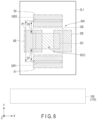
- FIG. 8 is a diagram for explaining Configuration Example 2 including a switching element SW.
- FIG. 11 is a diagram for explaining Configuration Example 3 including a switching element SW.
- FIG. 12 is a plan view showing an example of a display area DA.
- FIG. 20 is a cross-sectional view of a first substrate SUB 1 including a switching element SW and a first light-shielding wall 51 along line A-A′ shown in FIG. 19 .
- FIG. 21 is a cross-sectional view of the first substrate SUB 1 including the switching element SW along line B-B′ shown in FIG. 19 .
- FIG. 22 is a plan view showing of an example of a display area DA.
- FIG. 23 is a cross-sectional view of a first substrate SUB 1 including a switching element SW, a first light-shielding wall 51 , and a second light-shielding wall 52 along line A-A′ shown in FIG. 22 .
- FIG. 24 is a cross-sectional view of the first substrate SUB 1 including the switching element SW along line B-B′ shown in FIG. 22 .
- FIG. 25 is a plan view showing an example of a display area DA.
- FIG. 26 is a cross-sectional view of a first substrate SUB 1 including a switching element SW along line B-B′ shown in FIG. 25 .
- FIG. 27 is a cross-sectional view of a display device DSP.
- a display device comprises: a first substrate comprising a first transparent substrate, a scanning line disposed on the first transparent substrate, a first inorganic insulating film disposed on the scanning line, a signal line disposed on the first inorganic insulating film and intersecting the scanning line, a switching element provided with an oxide semiconductor disposed on the first inorganic insulating film and electrically connected to the scanning line and the signal line, a pixel electrode electrically connected to the switching element, and a first light-shielding wall; a second substrate comprising a second transparent substrate having a side surface, and a common electrode facing the pixel electrode; a liquid crystal layer disposed between the first substrate and the second substrate and containing a polymer-dispersed liquid crystal; and a light-emitting module disposed along the side surface, wherein the first inorganic insulating film, in planer view, includes a first groove formed between the oxide semiconductor and the light-emitting module, and the first light-shielding
- the display panel PNL comprises a first substrate SUB 1 , a second substrate SUB 2 , a liquid crystal layer LC containing polymer-dispersed liquid crystal, and a sealant SL.
- the first substrate SUB 1 and the second substrate SUB 2 are formed in a flat plate shape along an X-Y plane.
- the first substrate SUB 1 and the second substrate SUB 2 overlap each other in planar view.
- An area where the first substrate SUB 1 and the second substrate SUB 2 overlap includes a display area DA where images are displayed.
- the side surfaces 102 and 202 , the side surfaces 103 and 203 , and the side surfaces 104 and 204 overlap each other in planar view; however, they do not necessarily have to overlap.
- the side surface 201 does not overlap the side surface 101 , and is located between the side surface 101 and the display area DA.
- the first substrate SUB 1 has an extended portion Ex between the side surface 101 and the side surface 201 .
- the extended portion Ex corresponds to a portion of the first substrate SUB 1 that extends in the second direction Y from a portion overlapping the second substrate SUB 2 , and does not overlap the second substrate SUB 2 .
- the display panel PNL is formed in a rectangular shape extending in the first direction X.
- the side surfaces 101 and 102 and the side surfaces 201 and 202 are the side surfaces along the long side of the display panel PNL
- the side surfaces 103 and 104 and the side surfaces 203 and 204 are the side surfaces along the short side of the display panel PNL.
- the display panel PNL may be formed in a rectangular shape extending in the second direction Y, or in a square shape, or in any other polygonal shape, or in any other shape such as a circular shape or an elliptical shape.
- the light-emitting module 100 overlaps the extended portion Ex and is disposed along the side surface 201 of the second transparent substrate 20 .
- the sealant SL adheres the first substrate SUB 1 and the second substrate SUB 2 . Furthermore, the sealant SL is formed in the shape of a rectangular frame and surrounds the liquid crystal layer LC between the first substrate SUB 1 and the second substrate SUB 2 .
- the liquid crystal layer LC includes a polymer 31 and a liquid crystal molecule 32 .
- the polymer 31 is a liquid crystalline polymer.
- the polymer 31 is formed in the form of stripes extending along the first direction X and is arranged in the second direction Y.
- the liquid crystal molecule 32 is dispersed in gaps of the polymer 31 , and the long axis thereof is initially aligned along the first direction X.
- Each of the polymer 31 and liquid crystal molecule 32 has optical anisotropy or refractive index anisotropy. The responsiveness of the polymer 31 to electric fields is lower than that of liquid crystal molecule 32 to electric fields.
- the alignment direction of the polymer 31 hardly changes with or without an electric field.
- the alignment direction of the liquid crystal molecule 32 changes in response to the electric field when in a state where a voltage higher than or equal to a threshold is applied to the liquid crystal layer LC.
- the optical axes of the polymer 31 and liquid crystal molecule 32 are substantially parallel to each other, and light incident on the liquid crystal layer LC is almost completely transmitted through the liquid crystal layer LC (transparent state).
- the alignment direction of the liquid crystal molecules 32 changes, and the optical axes of the polymer 31 and liquid crystal molecules 32 intersect each other. Therefore, the light incident on the liquid crystal layer LC is scattered within the liquid crystal layer LC (scattered state).
- FIG. 2 is a plan view showing an area in the vicinity of the light-emitting module 100 .
- the light-emitting module 100 comprises a plurality of light-emitting elements 110 and a light guide 120 .
- the plurality of light-emitting elements 110 are arranged along the first direction X.
- the light guide 120 is formed in the form of a rod extending in the first direction X.
- the light guide 120 is located between the sealant SL and the light-emitting elements 110 .
- the display area DA comprises a plurality of pixels PX arranged in a matrix in the first direction X and the second direction Y. These pixels PX are shown by dotted lines in the drawing. Furthermore, each of the pixels PX comprises a pixel electrode PE shown by a solid square in the drawing.
- each pixel PX comprises a switching element SW.
- the switching element SW is, for example, configured by a thin-film transistor (TFT), and is electrically connected to a scanning line G and a signal line S.
- the scanning line G is electrically connected to the switching element SW in each of the pixels PX arranged in the first direction X.
- the signal line S is electrically connected to the switching element SW in each of the pixels PX arranged in the second direction Y.
- the pixel electrode PE is electrically connected to the switching element SW.
- a common electrode CE and a power supply line CL are disposed over the display area DA and its peripheral areas.
- a predetermined voltage Vcom is applied to the common electrode CE.
- Each of the pixel electrodes PE faces the common electrode CE in the third direction Z.
- the liquid crystal layer LC (in particular, the liquid crystal molecules 32 ) is driven by an electric field generated between the pixel electrode PE and the common electrode CE.
- a capacitance CS is formed, for example, between the power supply line CL and the pixel electrode PE.
- FIG. 3 is a cross-sectional view showing a configuration example of the display panel PNL shown in FIG. 1 .
- the switching element SW comprises an oxide semiconductor SC, a gate electrode GE, a source electrode SE, and a drain electrode DE.
- the gate electrode GE is electrically connected to the scanning line G.
- the oxide semiconductor SC overlaps the gate electrode GE.
- the source electrode SE is in contact with the oxide semiconductor SC and is electrically connected to the signal line S.
- the drain electrode DE is in contact with the oxide semiconductor SC and is electrically connected to the pixel electrode PE.
- the source electrode SE and the drain electrode DE are arranged at intervals in the first direction X.
- an area between the source electrode SE and the drain electrode DE corresponds to a channel SCC.
- the oxide semiconductor SC has a width W 1 in the first direction X.
- the channel SCC has a width W 11 in the first direction X.
- the width W 11 is smaller than the width W 1 (W 11 ⁇ W 1 ).
- a first light-shielding wall 51 is disposed in a manner filling the entire first groove GR 1 .
- the first light-shielding wall 51 extends in the first direction X.
- the first light-shielding wall 51 has a width W 13 in the first direction X.
- the width W 13 of the first light-shielding wall 51 is larger than the width W 12 of the first groove GR 1 (W 13 >W 12 ), and the width W 13 is larger than the width W 11 (W 13 >W 11 ).
- the width W 13 of the first light-shielding wall 51 may be smaller than the width W 12 of the first groove GR 1 (W 12 >W 13 ).
- the relationship that the width W 13 of the first light-shielding wall 51 is larger than the width W 11 (W 13 >W 11 ) remains unchanged.
- a plurality of scanning lines G each extend in the first direction X.
- a plurality of signal lines S each extend in the second direction Y and intersect the plurality of scanning lines G.
- the pixel PX corresponds to an area surrounded by two adjacent scanning lines G and two adjacent signal lines S.
- the switching element SW is located near the intersection of the scanning line G and the signal line S. Alternatively, the switching element SW may be disposed in a manner to overlap the intersection of the scanning line G and the signal line S.
- the first light-shielding wall 51 or the first groove GR 1 is located between the two adjacent scanning lines G.
- the scanning line GA is a scanning line located on a side close to the light-emitting module 100 , and is located between the scanning line GB and the light-emitting module 100 . Focusing on the first light-shielding wall 51 and the first groove GR 1 located between the scanning line GA and the scanning line GB, these first light-shielding wall 51 and first groove GR 1 are close to the scanning line GB (the scanning line on the far side from the light-emitting module 100 ).
- the distance between the first light-shielding wall 51 and the scanning line GB is smaller than the distance between the first light-shielding wall 51 and the scanning line GA.
- the distance between the first groove GR 1 and the scanning line GB is smaller than the distance between the first groove GR 1 and the scanning line GA.
- a pitch of the first light-shielding walls 51 (or the first grooves GR 1 ) arranged in the second direction Y is equivalent to a pitch of the pixel electrodes PE arranged in the second direction Y (hereinafter referred to as a pixel pitch), and is also equivalent to a pitch of the scanning lines G arranged in the second direction Y.
- the interval between the oxide semiconductor SC and the first light-shielding wall 51 (or the first groove GR 1 ) is smaller than the pixel pitch in the second direction Y and smaller than the pitch of the scanning lines G.
- FIG. 6 is a cross-sectional view of the first substrate SUB 1 including the switching element SW and the first light-shielding wall 51 along line A-A′ shown in FIG. 5 .
- FIG. 7 is a cross-sectional view of the first substrate SUB 1 including the switching element SW along line B-B′ shown in FIG. 5 .
- the scanning line G and the gate electrode GE are disposed on the main surface 10 B of the first transparent substrate 10 .
- the first inorganic insulating film IL 1 is disposed on the main surface 10 B and is also disposed on the scanning line G and the gate electrode GE.
- the oxide semiconductor SC including the channel SCC is disposed on the first inorganic insulating film IL 1 .
- the signal line S and the source electrode SE are disposed on the first inorganic insulating film IL 1 and intersect the scanning line G.
- the drain electrode DE is disposed on the first inorganic insulating film IL 1 .
- the source electrode SE and the drain electrode DE are in contact with the oxide semiconductor SC, respectively.
- the source electrode SE and the drain electrode DE are formed of the same material. In the oxide semiconductor SC, an area in contact with the source electrode SE and the drain electrode DE has a lower resistance than the channel SCC.
- the first groove GR 1 penetrates to the first transparent substrate 10 .
- the first light-shielding wall 51 is disposed in the first groove GR 1 and is in contact with the first transparent substrate 10 .
- a portion filled in the first groove GR 1 corresponds to a portion that blocks the light propagating through the first inorganic insulating film IL 1 .
- the first light-shielding wall 51 is located in the same layer as the source electrode SE and the drain electrode DE, and is formed of the same material as the source electrode SE and the drain electrode DE.
- a lower light-shielding wall integrally formed with the scanning line G may be disposed directly under the first groove GR 1 , as described later in FIG. 15 to FIG. 17 .
- a second inorganic insulating film IL 2 is disposed on the first inorganic insulating film IL 1 .
- the second inorganic insulating film IL 2 is also disposed on the signal line S, the source electrode SE, the drain electrode DE, the channel SCC of the oxide semiconductor SC, and the first light-shielding wall 51 .
- upper layers above the second inorganic insulating film IL 2 are not shown; however, for example, an organic insulating film is disposed on the second inorganic insulating film IL 2 , and these organic insulating film and second inorganic insulating film IL 2 correspond to the insulating film 11 shown in FIG. 3 .
- the scanning line G, the gate electrode GE, the signal line S, the source electrode SE, and the drain electrode DE are made of, for example, metal materials such as aluminum (Al), titanium (Ti), molybdenum (M), tungsten (W), silver (Ag), copper (Cu), and chromium (Cr), or an alloy combining these metal materials.
- metal materials such as aluminum (Al), titanium (Ti), molybdenum (M), tungsten (W), silver (Ag), copper (Cu), and chromium (Cr), or an alloy combining these metal materials.
- the first light-shielding wall 51 is formed of the same material as the signal line S, etc., and is configured by, for example, a titanium-based material/aluminum-based material/titanium-based material stacked layer body. Note that the material used to form the first light-shielding wall 51 is not limited to the above example. From the viewpoint of suppressing stray light due to reflection, it is desirable that the first light-shielding wall 51 is formed of a material with low reflectivity such as titanium, molybdenum, and tungsten.
- Each of the first inorganic insulating film IL 1 and the second inorganic insulating film IL 2 may be a single layer body or a stacked layer body. However, it is desirable that the first inorganic insulating film IL 1 and the second inorganic insulating film IL 2 include an oxide layer in contact with the oxide semiconductor SC. Such an oxide layer supplies oxygen to the oxide semiconductor SC and promotes oxidation or high resistance of the oxide semiconductor SC.
- the second inorganic insulating film IL 2 has a silicon oxide layer as the lower layer (the layer in contact with the channel SCC) and a silicon nitride layer as the upper layer.
- the lower layer is thicker than the upper layer.
- the thickness of the lower layer is about 300 nm
- the thickness of the upper layer is about 100 nm
- the total thickness of the second inorganic insulating film IL 2 is about 400 nm.
- FIG. 8 is a diagram for explaining Configuration Example 2 including the switching element SW.
- a first inorganic insulating film IL 1 has a second groove GR 2 .
- the second groove GR 2 extends in the first direction X and is almost parallel to a first groove GR 1 .
- An oxide semiconductor SC is located between the first groove GR 1 and the second groove GR 2 in the second direction Y.
- the second groove GR 2 has the same width as the first groove GR 1 .
- a channel SCC faces the second groove GR 2 and the second light-shielding wall 52 in the second direction Y.
- An interval D 2 along the second direction Y between the oxide semiconductor SC and the second groove GR 2 is equivalent to the interval D 1 , and is, for example, 1 to 25 ⁇ m.
- FIG. 9 is a plan view showing an example of the display area DA. Here, only a main part included in the first substrate SUB 1 is shown.
- the first light-shielding wall 51 (or the first groove GR 1 ) and the second light-shielding wall 52 (or the second groove GR 2 ) are located between two adjacent scanning lines G.
- these second light-shielding wall 52 and second groove GR 2 are close to the scanning line GA (the scanning line on a side close to the light-emitting module 100 ).
- the distance between the second light-shielding wall 52 and the scanning line GB is greater than the distance between the second light-shielding wall 52 and the scanning line GA.
- the distance between the second groove GR 2 and the scanning line GB is greater than the distance between the second groove GR 2 and the scanning line GA.
- first light-shielding wall 51 is located between the second light-shielding wall 52 and the scanning line GB in the second direction Y
- second light-shielding wall 52 is located between the scanning line GA and the first light-shielding wall 51 in the second direction Y.
- a pitch between the first light-shielding wall 51 and the second light-shielding wall 52 between the scanning line GA and the scanning line GB is larger than a pitch between the first light-shielding wall 51 and the second light-shielding wall 52 sandwiching the scanning line GA.
- a pitch of the second light-shielding walls 52 (or the second grooves GR 2 ) arranged in the second direction Y is equivalent to a pixel pitch in the second direction Y, and is also equivalent to a pitch of the scanning lines G arranged in the second direction Y.
- An interval between the oxide semiconductor SC and the second light-shielding wall 52 (or the second groove GR 2 ) is smaller than the pixel pitch in the second direction Y and smaller than the pitch of the scanning lines G.
- FIG. 10 is a cross-sectional view of the first substrate SUB 1 including the switching element SW, the first light-shielding wall 51 , and the second light-shielding wall 52 along line A-A′ shown in FIG. 9 .
- the cross section along line B-B′ shown in FIG. 9 is as shown in FIG. 7 ; therefore, the drawing thereof is omitted.
- each of the first groove GR 1 and the second groove GR 2 penetrates to the first transparent substrate 10 .
- the second light-shielding wall 52 is disposed in the second groove GR 2 and is in contact with the first transparent substrate 10 .
- a portion filled in the second groove GR 2 corresponds to a portion that blocks the light propagating through the first inorganic insulating film IL 1 .
- the second light-shielding wall 52 is located in the same layer as the source electrode SE and the drain electrode DE, and is formed of the same material as the source electrode SE and the drain electrode DE.
- a second inorganic insulating film IL 2 is disposed on the second light-shielding wall 52 .
- FIG. 11 is a diagram for explaining Configuration Example 3 including the switching element SW.
- a second inorganic insulating film IL 2 has a first through hole TH 1 that overlaps a first groove GR 1 .
- the first through hole TH 1 extends in the first direction X and has a width equivalent to that of the first groove GR 1 .
- the upper light-shielding wall 511 is disposed in a manner filling the entire first through hole TH 1 , and overlaps a first light-shielding wall 51 .
- the upper light-shielding wall 511 extends in the first direction X and has a width equivalent to that of the first light-shielding wall 51 .
- FIG. 12 is a plan view showing an example of the display area DA. Here, only a main part included in the first substrate SUB 1 is shown.
- a connecting electrode CN overlaps the scanning line G.
- the connecting electrode CN and the drain electrode DE are arranged in the first direction X.
- the metal layer M overlaps the scanning line G and extends in the first direction X.
- the metal layer M also overlaps a part of the signal line S, the oxide semiconductor SC, a part of the drain electrode DE, and the connecting electrode CN.
- the first light-shielding wall 51 is integrally formed with the signal line S.
- the upper light-shielding wall 511 overlaps the first light-shielding wall 51 and the signal line S.
- the upper light-shielding wall 511 is separated from the metal layer M.
- the upper light-shielding wall 511 (or the first through hole TH 1 ) is located between two adjacent scanning lines G in the same manner as the first light-shielding wall 51 described in Configuration Example 1. For example, focusing on the first light-shielding wall 51 and the first groove GR 1 located between scanning lines GA and GB, these upper light-shielding wall 511 and first through hole TH 1 are close to the scanning line GB.
- a pitch of the upper light-shielding walls 511 (or the first through holes TH 1 ) arranged in the second direction Y is equivalent to a pixel pitch in the second direction Y, and is also equivalent to a pitch of the scanning lines G.
- an illumination light emitted from the light-emitting module 100 travels along the second direction Y as shown by the dotted arrows, and is blocked by the first light-shielding wall 51 and the upper light-shielding wall 511 in the vicinity of the switching element SW. This prevents the illumination light from reaching the switching element SW, especially the oxide semiconductor SC.
- the first through hole TH 1 is formed directly above the first groove GR 1 and penetrates to the first light-shielding wall 51 .
- the upper light-shielding wall 511 is disposed in the first through hole TH 1 and is in contact with the first light-shielding wall 51 .
- a portion filled in the first through hole TH 1 corresponds to a portion that blocks the light propagating through the second inorganic insulating film IL 2 .
- the metal layer M is disposed on the second inorganic insulating film IL 2 and is located directly above the channel SCC. Furthermore, the metal layer M extends directly above the connecting electrode CN, is disposed in a contact hole CH 2 that penetrates the second inorganic insulating film IL 2 , and is in contact with the connecting electrode CN. As a result, the metal layer M is electrically connected to the scanning line G.
- the metal layer M is located in the same layer as the upper light-shielding wall 511 , and is formed of the same material as the upper light-shielding wall 511 .
- the upper light-shielding wall 511 and the metal layer M are configured, for example, by a molybdenum-based material/aluminum-based material/molybdenum-based material stacked layer body.
- the materials used to form the upper light-shielding wall 511 are not limited to the above example. From the viewpoint of suppressing stray light due to reflection, it is desirable that the upper light-shielding wall 511 be formed of a material with low reflectivity such as titanium, molybdenum, or tungsten.
- the upper light-shielding wall 511 is in contact with the first light-shielding wall 51 which is integrated with the signal line S, and is electrically connected to the signal line S. Therefore, the upper light-shielding wall 511 is separated from the metal layer M electrically connected to the scanning line G.
- the light propagating through the first inorganic insulating film IL 1 is blocked by the first light-shielding wall 51 .
- the light propagating through the second inorganic insulating film IL 2 is blocked by the upper light-shielding wall 511 . Therefore, the same effect as described above can be obtained.
- FIG. 15 is a diagram for explaining a modified example including the switching element SW.
- the lower light-shielding wall 512 overlaps a first light-shielding wall 51 and an upper light-shielding wall 511 .
- the lower light-shielding wall 512 extends in the first direction X.
- the lower light-shielding wall 512 is separated from a gate electrode GE.
- a first through hole TH 1 is formed directly above the first groove GR 1 and penetrates to the first light-shielding wall 51 .
- the upper light-shielding wall 511 is disposed in the first through hole TH 1 and is in contact with the first light-shielding wall 51 .
- the stacked layered body of the lower light-shielding wall 512 , the first light-shielding wall 51 , and the upper light-shielding wall 511 is configured to block the illumination light from the light-emitting module.
- One end portion of the first light-shielding wall 51 extending in the first direction X faces a source electrode SE in the second direction Y. Furthermore, the other end portion of the first light-shielding wall 51 faces a drain electrode DE in the second direction Y.
- the channel SCC and the metal layer M face the first light-shielding wall 51 in the second direction Y.
- the first light-shielding wall 51 is separated from the signal line S.
- the signal line S meanders so as to avoid the first light-shielding wall 51 .
- the first light-shielding wall 51 is separated from the metal layer M.
- a pitch of the first light-shielding walls 51 arranged in the second direction Y is equivalent to a pixel pitch in the second direction Y, and is also equivalent to a pitch of the scanning lines G.
- an illumination light emitted from the light-emitting module 100 travels along the second direction Y as shown by the dotted arrows, and is blocked by the first light-shielding wall 51 in the vicinity of the switching element SW. This prevents the illumination light from reaching the switching element SW, especially the oxide semiconductor SC.
- FIG. 20 is a cross-sectional view of the first substrate SUB 1 including the switching element SW and the first light-shielding wall 51 along line A-A′ shown in FIG. 19 .
- FIG. 21 is a cross-sectional view of the first substrate SUB 1 including the switching element SW along line B-B′ shown in FIG. 19 .
- the first through hole TH 1 is formed directly above the first groove GR 1 .
- the first groove GR 1 and the first through hole TH 1 penetrate to the first transparent substrate 10 .
- the first light-shielding wall 51 is disposed in the first groove GR 1 and the first through hole TH 1 , and is in contact with the first transparent substrate 10 .
- a portion filled in the first groove GR 1 corresponds to a portion that blocks the light propagating through a first inorganic insulating film IL 1
- a portion filled in the first through hole TH 1 corresponds to a portion that blocks the light propagating through the second inorganic insulating film IL 2 .
- the first inorganic insulating film IL 1 may be penetrated continuously with the second inorganic insulating film IL 2 so that the second inorganic insulating film IL 2 and the first inorganic insulating film IL 1 are collectively opened by the first through hole TH 1 .
- the metal layer M is disposed on the second inorganic insulating film IL 2 and is located directly above the channel SCC.
- the metal layer M extends directly above the scanning line G, is disposed in a contact hole CH 1 penetrating through the first inorganic insulating film IL 1 and a contact hole CH 2 penetrating through the second inorganic insulating film IL 2 , and is in contact with the scanning line G.
- the metal layer M is electrically connected to the scanning line G.
- the metal layer M is located in the same layer as the first light-shielding wall 51 , and is formed of the same material as the first light-shielding wall 51 .
- the first inorganic insulating film IL 1 may be penetrated continuously with the second inorganic insulating film IL 2 so that the second inorganic insulating film IL 2 and the first inorganic insulating film IL 1 are collectively opened by the contact hole CH 2 .
- the first light-shielding wall 51 is separated from the signal line S. For this reason, the first light-shielding wall 51 may be connected to the metal layer M electrically connected to the scanning line G.
- the same effect as described above can be obtained.
- FIG. 22 is a plan view showing an example of the display area DA. Here, only a main part included in the first substrate SUB 1 is shown.
- the oxide semiconductor SC is located between the first groove GR 1 (first through hole TH 1 ) and the second groove GR 2 (second through hole TH 2 ) in the second direction Y. In addition, the oxide semiconductor SC is located between a signal line S and the third groove GR 3 (third through hole TH 3 ) in the first direction X.
- a pitch between the first light-shielding wall 51 (or the first groove GR 1 ) and the second light-shielding wall 52 (or the second groove GR 2 ) sandwiching one oxide semiconductor SC is smaller than a pixel pitch in the second direction Y and smaller than a pitch of the scanning lines G.
- the first light-shielding wall 51 is disposed in the first groove GR 1 and the first through hole TH 1 , and is in contact with the first transparent substrate 10 .
- the second light-shielding wall 52 is disposed in the second groove GR 2 and the second through hole TH 2 , and is in contact with the first transparent substrate 10 .
- the first light-shielding wall 51 and the second light-shielding wall 52 are separated from the metal layer M.
- the same effect as described above can be obtained.
- FIG. 25 is a plan view showing an example of the display area DA. Here, only a main part included in the first substrate SUB 1 is shown.
- first groove GR 1 and the first through hole TH 1 overlap each other
- a second groove GR 2 and a second through hole TH 2 overlap each other
- a third groove GR 3 and a third through hole TH 3 overlap each other
- a fourth groove GR 4 and a fourth through hole TH 4 overlap each other.
- the first groove GR 1 , the first through hole TH 1 , the second groove GR 2 , and the second through hole TH 2 extend in the first direction X, respectively.
- the third groove GR 3 , the third through hole TH 3 , the fourth groove GR 4 , and the fourth through hole TH 4 extend in the second direction Y.
- the oxide semiconductor SC is located between the first groove GR 1 (first through hole TH 1 ) and the second groove GR 2 (second through hole TH 2 ) in the second direction Y.
- the oxide semiconductor SC is located between the third groove GR 3 (third through hole TH 3 ) and the fourth groove GR 4 (fourth through hole TH 4 ) in the first direction X.
- the metal layer M and the auxiliary metal layer AM overlap the scanning line G.
- the metal layer M further overlaps a part of the signal line S, the oxide semiconductor SC, and a part of the drain electrode DE.
- the metal layer M is disposed on the third groove GR 3 and the third through hole TH 3 .
- the auxiliary metal layer AM is separated from the metal layer M. Note that the auxiliary metal layer AM may be connected to the metal layer M.
- the auxiliary metal layer AM is disposed in the fourth groove GR 4 and the fourth through hole TH 4 .
- a pitch between the first light-shielding wall 51 (or the first groove GR 1 ) and the second light-shielding wall 52 (or the second groove GR 2 ) sandwiching one oxide semiconductor SC is smaller than a pixel pitch in the second direction Y and smaller than a pitch of the scanning lines G.
- a pitch between the third and fourth grooves GR 3 and GR 4 sandwiching one oxide semiconductor SC is smaller than the pixel pitch in the first direction X and smaller than a pitch of the signal lines S.
- the light traveling along the first direction X due to scattering or reflection is also blocked in the vicinity of the switching element SW. This prevents the illumination light from reaching the switching element SW, especially the oxide semiconductor SC.
- FIG. 26 is a cross-sectional view of the first substrate SUB 1 including the switching element SW along line B-B′ shown in FIG. 25 .
- the cross section of the first substrate SUB 1 including the switching element SW, the first light-shielding wall 51 , and the second light-shielding wall 52 along line A-A′ shown in FIG. 25 is as shown in FIG. 23 ; therefore, the drawing thereof is omitted.
- a portion filled in the third groove GR 3 corresponds to a portion that blocks the light propagating through the first inorganic insulating film IL 1
- a portion filled in the third through hole TH 3 corresponds to a portion that blocks the light propagating through the second inorganic insulating film IL 2
- a portion filled in the fourth groove GR 4 corresponds to a portion that blocks the light propagating through the first inorganic insulating film IL 1
- a portion filled in the fourth through hole TH 4 corresponds to a portion that blocks the light propagating through the second inorganic insulating film IL 2 .
- the same effect as described above can be obtained.
- FIG. 27 is a cross-sectional view of the display device DSP. Only a main part of the display panel PNL is shown in a simplified form.
- the display panel PNL comprises a third transparent substrate 30 .
- a main surface (inner surface) 30 A of the third transparent substrate 30 faces the main surface 20 B of the second transparent substrate 20 in the third direction Z.
- An adhesive layer AD adheres the second transparent substrate 20 and the third transparent substrate 30 .
- the third transparent substrate 30 is, for example, a glass substrate, but may also be an insulating substrate such as a plastic substrate.
- the third transparent substrate 30 has a refractive index equivalent to that of the first transparent substrate 10 and the second transparent substrate 20 .
- the adhesive layer AD has a refractive index equivalent to that of each of the second transparent substrate 20 and the third transparent substrate 30 .
- a side surface 301 of the third transparent substrate 30 is located directly above a side surface 201 of the second transparent substrate 20 .
- the light-emitting element 110 of the light-emitting module 100 is electrically connected to a wiring substrate F and is disposed between the first substrate SUB 1 and the wiring substrate F in the third direction Z.
- the light guide 120 is disposed between the light-emitting element 110 and the side surface 201 , and between the light-emitting element 110 and the side surface 301 in the second direction Y.
- the light guide 120 is adhered to the wiring substrate F by an adhesive layer AD 1 and to the first substrate SUB 1 by an adhesive layer AD 2 .
- the light-emitting element 110 emits the light L 1 toward the light guide 120 .
- the light L 1 emitted from the light-emitting element 110 propagates along the direction of the arrow indicating the second direction Y, is transmitted through the light guide 120 , is incident on the second transparent substrate 20 from the side surface 201 , and is incident on the third transparent substrate 30 from the side surface 301 .
- the light L 1 incident on the second transparent substrate 20 and the third transparent substrate 30 propagates inside the display panel PNL while being repeatedly reflected.
- the light L 1 incident on the liquid crystal layer LC to which no voltage is applied is transmitted through the liquid crystal layer LC with little scattering.
- the light L 1 incident on the liquid crystal layer LC to which the voltage is applied is scattered by the liquid crystal layer LC.
- the display device DSP is observable from the main surface 10 A side of the first transparent substrate 10 and from a main surface 30 B side of the third transparent substrate 30 .
- the display device DSP is observed from the main surface 10 A side or the main surface 30 B side, the background of the display device DSP can be observed through the display device DSP.
- the switching element SW of each pixel PX comprises a transparent oxide semiconductor SC, and the transmittance can also be improved by omitting the light-shielding layer overlapping the oxide semiconductor SC in the third direction Z.
Landscapes
- Physics & Mathematics (AREA)
- Nonlinear Science (AREA)
- Chemical & Material Sciences (AREA)
- General Physics & Mathematics (AREA)
- Crystallography & Structural Chemistry (AREA)
- Mathematical Physics (AREA)
- Optics & Photonics (AREA)
- Engineering & Computer Science (AREA)
- Microelectronics & Electronic Packaging (AREA)
- Dispersion Chemistry (AREA)
- Liquid Crystal (AREA)
- Geometry (AREA)
- Devices For Indicating Variable Information By Combining Individual Elements (AREA)
Abstract
Description
Claims (16)
Applications Claiming Priority (3)
| Application Number | Priority Date | Filing Date | Title |
|---|---|---|---|
| JP2021072049A JP7570969B2 (en) | 2021-04-21 | 2021-04-21 | Display device |
| JP2021-072049 | 2021-04-21 | ||
| JPJP2021-072049 | 2021-04-21 |
Publications (2)
| Publication Number | Publication Date |
|---|---|
| US20220342264A1 US20220342264A1 (en) | 2022-10-27 |
| US11609463B2 true US11609463B2 (en) | 2023-03-21 |
Family
ID=83695192
Family Applications (1)
| Application Number | Title | Priority Date | Filing Date |
|---|---|---|---|
| US17/723,468 Active 2042-04-19 US11609463B2 (en) | 2021-04-21 | 2022-04-19 | Display device |
Country Status (2)
| Country | Link |
|---|---|
| US (1) | US11609463B2 (en) |
| JP (1) | JP7570969B2 (en) |
Cited By (1)
| Publication number | Priority date | Publication date | Assignee | Title |
|---|---|---|---|---|
| US12347380B2 (en) | 2023-03-24 | 2025-07-01 | Samsung Display Co., Ltd. | Display apparatus |
Citations (3)
| Publication number | Priority date | Publication date | Assignee | Title |
|---|---|---|---|---|
| US20020089617A1 (en) * | 1999-04-16 | 2002-07-11 | Tamaki Fukata | Liquid crystal display |
| US20180031758A1 (en) | 2016-08-01 | 2018-02-01 | Japan Display Inc. | Display apparatus |
| JP2020091400A (en) | 2018-12-05 | 2020-06-11 | 株式会社ジャパンディスプレイ | Display |
Family Cites Families (2)
| Publication number | Priority date | Publication date | Assignee | Title |
|---|---|---|---|---|
| JP6901382B2 (en) | 2017-11-29 | 2021-07-14 | パナソニック液晶ディスプレイ株式会社 | Liquid crystal display panel |
| JP7237633B2 (en) | 2019-02-14 | 2023-03-13 | 株式会社ジャパンディスプレイ | Display device |
-
2021
- 2021-04-21 JP JP2021072049A patent/JP7570969B2/en active Active
-
2022
- 2022-04-19 US US17/723,468 patent/US11609463B2/en active Active
Patent Citations (5)
| Publication number | Priority date | Publication date | Assignee | Title |
|---|---|---|---|---|
| US20020089617A1 (en) * | 1999-04-16 | 2002-07-11 | Tamaki Fukata | Liquid crystal display |
| US20180031758A1 (en) | 2016-08-01 | 2018-02-01 | Japan Display Inc. | Display apparatus |
| JP2018021974A (en) | 2016-08-01 | 2018-02-08 | 株式会社ジャパンディスプレイ | Display |
| JP2020091400A (en) | 2018-12-05 | 2020-06-11 | 株式会社ジャパンディスプレイ | Display |
| US20210286226A1 (en) | 2018-12-05 | 2021-09-16 | Japan Display Inc. | Display device |
Cited By (1)
| Publication number | Priority date | Publication date | Assignee | Title |
|---|---|---|---|---|
| US12347380B2 (en) | 2023-03-24 | 2025-07-01 | Samsung Display Co., Ltd. | Display apparatus |
Also Published As
| Publication number | Publication date |
|---|---|
| JP2022166675A (en) | 2022-11-02 |
| JP7570969B2 (en) | 2024-10-22 |
| US20220342264A1 (en) | 2022-10-27 |
Similar Documents
| Publication | Publication Date | Title |
|---|---|---|
| US12013613B2 (en) | Display device | |
| US12411374B2 (en) | Display device including a liquid crystal layer including polymers and liquid crystal molecules and switching between a scattering state and a transmitting state | |
| US12392955B2 (en) | Display device | |
| US12001107B2 (en) | Display device | |
| US12025899B2 (en) | Display device | |
| US11809049B2 (en) | Display device | |
| US20240094585A1 (en) | Display device | |
| US11703735B2 (en) | Display device | |
| US11609463B2 (en) | Display device | |
| US11977305B2 (en) | Display device | |
| US12345982B2 (en) | Display device | |
| US20220035189A1 (en) | Display device |
Legal Events
| Date | Code | Title | Description |
|---|---|---|---|
| AS | Assignment |
Owner name: JAPAN DISPLAY INC., JAPAN Free format text: ASSIGNMENT OF ASSIGNORS INTEREST;ASSIGNOR:HANADA, AKIHIRO;REEL/FRAME:059631/0213 Effective date: 20220322 |
|
| FEPP | Fee payment procedure |
Free format text: ENTITY STATUS SET TO UNDISCOUNTED (ORIGINAL EVENT CODE: BIG.); ENTITY STATUS OF PATENT OWNER: LARGE ENTITY |
|
| STPP | Information on status: patent application and granting procedure in general |
Free format text: NON FINAL ACTION MAILED |
|
| STPP | Information on status: patent application and granting procedure in general |
Free format text: RESPONSE TO NON-FINAL OFFICE ACTION ENTERED AND FORWARDED TO EXAMINER |
|
| STPP | Information on status: patent application and granting procedure in general |
Free format text: NOTICE OF ALLOWANCE MAILED -- APPLICATION RECEIVED IN OFFICE OF PUBLICATIONS |
|
| STCF | Information on status: patent grant |
Free format text: PATENTED CASE |
|
| AS | Assignment |
Owner name: MAGNOLIA WHITE CORPORATION, JAPAN Free format text: ASSIGNMENT OF ASSIGNORS INTEREST;ASSIGNOR:JAPAN DISPLAY INC.;REEL/FRAME:072130/0313 Effective date: 20250625 Owner name: MAGNOLIA WHITE CORPORATION, JAPAN Free format text: ASSIGNMENT OF ASSIGNOR'S INTEREST;ASSIGNOR:JAPAN DISPLAY INC.;REEL/FRAME:072130/0313 Effective date: 20250625 |