US11569380B2 - Semiconductor structure - Google Patents

Semiconductor structure Download PDF

Info

Publication number
US11569380B2
US11569380B2 US17/366,053 US202117366053A US11569380B2 US 11569380 B2 US11569380 B2 US 11569380B2 US 202117366053 A US202117366053 A US 202117366053A US 11569380 B2 US11569380 B2 US 11569380B2
Authority
US
United States
Prior art keywords
salicide
semiconductor structure
corners
overlapping region
gate structure
Prior art date
Legal status (The legal status is an assumption and is not a legal conclusion. Google has not performed a legal analysis and makes no representation as to the accuracy of the status listed.)
Active
Application number
US17/366,053
Other versions
US20230006062A1 (en
Inventor
Wei-Hsuan Chang
Ming-Hua Tsai
Chin-Chia Kuo
Current Assignee (The listed assignees may be inaccurate. Google has not performed a legal analysis and makes no representation or warranty as to the accuracy of the list.)
United Microelectronics Corp
Original Assignee
United Microelectronics Corp
Priority date (The priority date is an assumption and is not a legal conclusion. Google has not performed a legal analysis and makes no representation as to the accuracy of the date listed.)
Filing date
Publication date
Application filed by United Microelectronics Corp filed Critical United Microelectronics Corp
Priority to US17/366,053 priority Critical patent/US11569380B2/en
Assigned to UNITED MICROELECTRONICS CORP. reassignment UNITED MICROELECTRONICS CORP. ASSIGNMENT OF ASSIGNORS INTEREST (SEE DOCUMENT FOR DETAILS). Assignors: TSAI, MING-HUA, CHANG, WEI-HSUAN, KUO, CHIN-CHIA
Publication of US20230006062A1 publication Critical patent/US20230006062A1/en
Application granted granted Critical
Publication of US11569380B2 publication Critical patent/US11569380B2/en
Active legal-status Critical Current
Anticipated expiration legal-status Critical

Links

Images

Classifications

    • HELECTRICITY
    • H10SEMICONDUCTOR DEVICES; ELECTRIC SOLID-STATE DEVICES NOT OTHERWISE PROVIDED FOR
    • H10DINORGANIC ELECTRIC SEMICONDUCTOR DEVICES
    • H10D62/00Semiconductor bodies, or regions thereof, of devices having potential barriers
    • H10D62/10Shapes, relative sizes or dispositions of the regions of the semiconductor bodies; Shapes of the semiconductor bodies
    • H10D62/124Shapes, relative sizes or dispositions of the regions of semiconductor bodies or of junctions between the regions
    • H10D62/126Top-view geometrical layouts of the regions or the junctions
    • HELECTRICITY
    • H10SEMICONDUCTOR DEVICES; ELECTRIC SOLID-STATE DEVICES NOT OTHERWISE PROVIDED FOR
    • H10DINORGANIC ELECTRIC SEMICONDUCTOR DEVICES
    • H10D30/00Field-effect transistors [FET]
    • H10D30/60Insulated-gate field-effect transistors [IGFET]
    • H10D30/601Insulated-gate field-effect transistors [IGFET] having lightly-doped drain or source extensions, e.g. LDD IGFETs or DDD IGFETs 
    • H10D30/605Insulated-gate field-effect transistors [IGFET] having lightly-doped drain or source extensions, e.g. LDD IGFETs or DDD IGFETs  having significant overlap between the lightly-doped extensions and the gate electrode
    • H01L29/7836
    • H01L29/458
    • HELECTRICITY
    • H10SEMICONDUCTOR DEVICES; ELECTRIC SOLID-STATE DEVICES NOT OTHERWISE PROVIDED FOR
    • H10DINORGANIC ELECTRIC SEMICONDUCTOR DEVICES
    • H10D30/00Field-effect transistors [FET]
    • H10D30/01Manufacture or treatment
    • H10D30/021Manufacture or treatment of FETs having insulated gates [IGFET]
    • H10D30/0212Manufacture or treatment of FETs having insulated gates [IGFET] using self-aligned silicidation
    • HELECTRICITY
    • H10SEMICONDUCTOR DEVICES; ELECTRIC SOLID-STATE DEVICES NOT OTHERWISE PROVIDED FOR
    • H10DINORGANIC ELECTRIC SEMICONDUCTOR DEVICES
    • H10D30/00Field-effect transistors [FET]
    • H10D30/60Insulated-gate field-effect transistors [IGFET]
    • HELECTRICITY
    • H10SEMICONDUCTOR DEVICES; ELECTRIC SOLID-STATE DEVICES NOT OTHERWISE PROVIDED FOR
    • H10DINORGANIC ELECTRIC SEMICONDUCTOR DEVICES
    • H10D30/00Field-effect transistors [FET]
    • H10D30/60Insulated-gate field-effect transistors [IGFET]
    • H10D30/67Thin-film transistors [TFT]
    • H10D30/6729Thin-film transistors [TFT] characterised by the electrodes
    • H10D30/6737Thin-film transistors [TFT] characterised by the electrodes characterised by the electrode materials
    • HELECTRICITY
    • H10SEMICONDUCTOR DEVICES; ELECTRIC SOLID-STATE DEVICES NOT OTHERWISE PROVIDED FOR
    • H10DINORGANIC ELECTRIC SEMICONDUCTOR DEVICES
    • H10D30/00Field-effect transistors [FET]
    • H10D30/60Insulated-gate field-effect transistors [IGFET]
    • H10D30/67Thin-film transistors [TFT]
    • H10D30/674Thin-film transistors [TFT] characterised by the active materials
    • H10D30/6741Group IV materials, e.g. germanium or silicon carbide
    • H10D30/6743Silicon

Definitions

  • the present invention relates to the field of semiconductor manufacturing processes, in particular to a semiconductor structure including salicide layer.
  • Field effect transistors are important electronic devices in the fabrication of integrated circuits, and as the size of the semiconductor device shrinks, fabrications of the transistors and interconnects have to be improved for fabricating transistors with smaller sizes and higher quality.
  • contact plugs are often utilized for interconnection purposes, in which the contact plugs are composed of conducting metals such as tungsten or copper to electrically connect the gate, source, and drain to upper level interconnect layers.
  • the contact plugs are composed of conducting metals such as tungsten or copper to electrically connect the gate, source, and drain to upper level interconnect layers.
  • salicide layers are often formed over the surface of the gate structure and the source/drain region to improve the Ohmic contact between the contact plugs and the gate structure and the source/drain region.
  • a self-align salicide (salicide) process has been widely utilized to fabricate the salicide layers.
  • the salicide process after forming a salicide block (SAB) layer over non-salicide regions that are defined by a layout pattern according to a design rule provided from clients, includes steps of disposing a metal layer comprised of cobalt, titanium, or nickel on a source/drain region and a gate structure, and performing a rapid thermal process (RTP), thus the metal layer reacts with the silicon contained within the gate structure and the source/drain region to form a metal salicide.
  • SAB salicide block
  • FIG. 1 shows a top view of a transistor device.
  • a substrate 10 is provided, on which an active area AA is defined, a gate structure 12 spans the active area AA, the active areas AA on both sides of the gate structure 12 are defined as source regions 14 and drain regions 16 , respectively, and a plurality of contact structures 22 are located on and electrically connected to the source regions 14 and drain regions 16 .
  • a salicide layer 20 can be formed on the source region 14 and the drain region 16 .
  • the applicant has found that when salicide layer 20 is formed on the whole source region 14 and drain region 16 , leakage current is easily generated at the interface between gate structure 12 and active area AA (especially at the corner A, the corner B, the corner C and the corner D shown in FIG. 1 ), which affects the device performance.
  • a semiconductor structure in one aspect of the present invention, includes a substrate, and an active area is defined thereon, a gate structure spanning the active area, wherein the overlapping range of the gate structure and the active area is defined as an overlapping region, and the overlapping region includes four corners, and at least one salicide block covering the four corners of the overlapping region.
  • the present invention is characterized in that the shape of salicide block is designed so that salicide block covers at least the corners at the interface of the gate structure and the active area, but does not cover the long sides of both sides of the gate structure.
  • the salicide layer formed later will not cover the corners at the interface of the gate structure and the active area, which can prevent the leakage current of the gate structure from flowing into the salicide layer. Therefore, the semiconductor structure with salicide layer of the present invention has the advantages of preventing leakage current, improving product yield, and being compatible with the existing process.
  • FIG. 1 shows a top view of a conventional transistor device.
  • FIG. 2 - 3 shows a top view of a semiconductor structure according to the first preferred embodiment of the present invention.
  • FIG. 4 shows a top view of a semiconductor structure according to another embodiment of the present invention.
  • FIG. 5 shows a top view of a semiconductor structure according to another embodiment of the present invention.
  • FIG. 2 - 3 shows a top view of a semiconductor structure according to the first preferred embodiment of the present invention.
  • a substrate 10 such as a silicon substrate, is provided, on which an active area (AA) and a shallow trench isolation (STI) surrounding the active area are formed.
  • the active area AA comprises the same material as the silicon substrate, and the shallow trench isolation STI comprises an insulating layer (such as silicon oxide).
  • a gate structure 12 is formed on the substrate 10 , with spacers 13 beside the gate structure 12 , and the active areas AA on both sides of the gate structure 12 are defined as a source region 14 and a drain region 16 , respectively.
  • the gate structure described here is not limited to polysilicon gate or metal gate, and the spacer 13 is an insulating material such as silicon oxide or silicon nitride. Until this step, it is similar to the structure described in the prior art (please refer to FIG. 1 ), in which the substrate 10 , the active area AA, the shallow trench isolation STI, the gate structure 12 , the source region 14 , the drain region 16 and other components described here belong to the conventional technology in this field, and are not described in detail here.
  • the overlapping range between the gate structure 12 and the active area AA is defined as an overlapping region OR, and the overlapping region OR includes four corners (corner A, corner B, corner C and corner D).
  • the overlapping region OR includes four corners (corner A, corner B, corner C and corner D).
  • the salicide layer located at corner A-D is easy to generate leakage current.
  • the Ohmic resistance cannot be reduced.
  • a salicide block (SAB) 19 is formed to cover at least the corners A to D.
  • a salicide process is performed to form a salicide layer 20 in the region except the salicide block 19 .
  • the salicide process mentioned above comprises forming a metal layer (such as cobalt, titanium, or nickel, etc.) and performing a heating step (RTP).
  • RTP heating step
  • the salicide block 19 is designed to cover at least the corners A to D of the overlapping region OR. As shown in FIG. 2 , the formed salicide block 19 has four patterns separated from each other, each of which is a rectangular pattern, covering one of the corners A to D respectively. In addition, in this embodiment, the total area of salicide block 19 is less than 1/10 of the total area of source region 14 and drain region 16 , but it is not limited to this. Besides, the salicide block formed in the present invention can be formed together with other salicide block processes (for example, in the original process, salicide block was formed on devices such as resistors and I/O regions), so the salicide block formed in the present invention does not use additional steps.
  • a salicide process is performed. As shown in FIG. 3 , the salicide layer 20 is formed on the source region 14 and the drain region 16 , but it is not formed at the corner A-D. Then, a contact structure 22 is formed on the salicide layer 20 .
  • the salicide layer 20 in this embodiment can reduce the interface resistance between the source region 14 /the drain region 16 and the contact structure 22 , but it is not located at the corner A-D, so the probability of leakage current caused by salicide being located at the corner can be reduced.
  • the salicide layer 20 in this embodiment does not cover the corners A-D, it will be located beside the long sides of the gate structure 12 , that is, adjacent to the two long sides of the overlapping region OR. In other words, the salicide layer 20 in this embodiment directly contacts the spacer 13 on both sides of the middle part of the gate structure 12 . According to the observation results of the applicant, when the salicide layer 20 is adjacent to the long sides of the gate structure 12 , the control effect of the gate structure on electrical properties is better.
  • the shape of the salicide block 19 can be changed, so that salicide layer 20 with different shapes can be produced.
  • the following paragraphs will illustrate different shapes of salicide layer in different embodiments of the present invention. To simplify the description, the following description will detail the dissimilarities among the different embodiments and the identical features will not be redundantly described. In order to compare the differences between the embodiments easily, the identical components in each of the following embodiments are marked with identical symbols.
  • a salicide block 19 A has a different shape from the salicide block 19 shown in FIG. 2 .
  • the salicide block 19 A in this embodiment includes two patterns separated from each other, one pattern covering two corners (such as corner A and corner B) of the overlapping region OR, and the other pattern covering the other two corners (such as corner C and corner D) of the overlapping region OR, the two patterns are rectangular shape patterns, but not limited to this.
  • the shape of the salicide block is changed, so the shape of the salicide layer formed later will also be changed.
  • the salicide layer in this embodiment still does not cover the corner A-D, thus reducing the probability of leakage current.
  • a salicide block 19 B has a different shape from the salicide block 19 shown in FIG. 2 .
  • salicide block 19 B includes a frame shape pattern covering the four corners of the overlapping region, but it is not limited to this.
  • the shape of the salicide block is changed, so the shape of the salicide layer formed later will also be changed.
  • the salicide layer in this embodiment still does not cover the corner A-D, thus reducing the probability of leakage current.
  • a semiconductor structure in one aspect of the present invention, includes a substrate, and an active area is defined thereon, a gate structure spanning the active area, wherein the overlapping range of the gate structure and the active area is defined as an overlapping region, and the overlapping region includes four corners, and at least one salicide block covering the four corners of the overlapping region.
  • the overlapping region includes two long sides, and the salicide block does not cover a middle part of the two long sides.
  • the salicide block includes four patterns separated from each other, and wherein the four patterns covers the four corners of the overlapping region respectively.
  • the four patterns are rectangular shape patterns.
  • the salicide block comprises two patterns separated from each other, one pattern covering two corners of the overlapping region and the other pattern covering the other two corners of the overlapping region.
  • the two patterns are rectangular shape patterns.
  • the salicide block includes a pattern covering the four corners of the overlapping region.
  • the pattern is a frame shape pattern.
  • the active area on both sides of the gate structure is defined as a source/drain region, and further comprising at least one contact structure located on the source/drain region.
  • the present invention further comprising at least one salicide layer disposed on the source/drain region, wherein the salicide layer does not overlap with the four corners of the overlapping region.
  • the area of each salicide block is less than 1/10 of the area of the source/drain region.
  • parts of the salicide layer directly contacts the two spacers which is disposed on both sides of the gate structure in a middle part of the gate structure.
  • the present invention is characterized in that the shape of salicide block is designed so that salicide block covers at least the corners at the interface of the gate structure and the active area, but does not cover the long sides of both sides of the gate structure.
  • the salicide layer formed later will not cover the corners at the interface of the gate structure and the active area, which can prevent the leakage current of the gate structure from flowing into the salicide layer. Therefore, the semiconductor structure with salicide layer of the present invention has the advantages of preventing leakage current, improving product yield, and being compatible with the existing process.

Landscapes

  • Insulated Gate Type Field-Effect Transistor (AREA)

Abstract

A semiconductor structure is provided, and the semiconductor structure includes a substrate, and an active area is defined thereon, a gate structure spanning the active area, wherein the overlapping range of the gate structure and the active area is defined as an overlapping region, and the overlapping region includes four corners, and at least one salicide block covering the four corners of the overlapping region.

Description

BACKGROUND OF THE INVENTION 1. Field of the Invention
The present invention relates to the field of semiconductor manufacturing processes, in particular to a semiconductor structure including salicide layer.
2. Description of the Prior Art
Field effect transistors are important electronic devices in the fabrication of integrated circuits, and as the size of the semiconductor device shrinks, fabrications of the transistors and interconnects have to be improved for fabricating transistors with smaller sizes and higher quality.
Conventionally, after forming the transistors, contact plugs are often utilized for interconnection purposes, in which the contact plugs are composed of conducting metals such as tungsten or copper to electrically connect the gate, source, and drain to upper level interconnect layers. Furthermore, salicide layers are often formed over the surface of the gate structure and the source/drain region to improve the Ohmic contact between the contact plugs and the gate structure and the source/drain region. For example, a self-align salicide (salicide) process has been widely utilized to fabricate the salicide layers. The salicide process, after forming a salicide block (SAB) layer over non-salicide regions that are defined by a layout pattern according to a design rule provided from clients, includes steps of disposing a metal layer comprised of cobalt, titanium, or nickel on a source/drain region and a gate structure, and performing a rapid thermal process (RTP), thus the metal layer reacts with the silicon contained within the gate structure and the source/drain region to form a metal salicide.
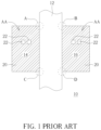
As mentioned above, the salicide is utilized to reduce contact resistance of diffusion regions in typical logic circuits. However, the applicant found that if salicide is excessively formed, it will easily lead to leakage current of the device. For example, FIG. 1 shows a top view of a transistor device. In the device shown in FIG. 1 , a substrate 10 is provided, on which an active area AA is defined, a gate structure 12 spans the active area AA, the active areas AA on both sides of the gate structure 12 are defined as source regions 14 and drain regions 16, respectively, and a plurality of contact structures 22 are located on and electrically connected to the source regions 14 and drain regions 16. Generally, in order to reduce the resistance between the contact structure 22 and the source region 14/the drain region 16, a salicide layer 20 can be formed on the source region 14 and the drain region 16. However, the applicant has found that when salicide layer 20 is formed on the whole source region 14 and drain region 16, leakage current is easily generated at the interface between gate structure 12 and active area AA (especially at the corner A, the corner B, the corner C and the corner D shown in FIG. 1 ), which affects the device performance.
Therefore, there is a need for an improved semiconductor structure to solve the above problems.
SUMMARY OF THE INVENTION
In one aspect of the present invention, a semiconductor structure is provided, and the semiconductor structure includes a substrate, and an active area is defined thereon, a gate structure spanning the active area, wherein the overlapping range of the gate structure and the active area is defined as an overlapping region, and the overlapping region includes four corners, and at least one salicide block covering the four corners of the overlapping region.
To sum up, the present invention is characterized in that the shape of salicide block is designed so that salicide block covers at least the corners at the interface of the gate structure and the active area, but does not cover the long sides of both sides of the gate structure. In this way, the salicide layer formed later will not cover the corners at the interface of the gate structure and the active area, which can prevent the leakage current of the gate structure from flowing into the salicide layer. Therefore, the semiconductor structure with salicide layer of the present invention has the advantages of preventing leakage current, improving product yield, and being compatible with the existing process.
These and other objectives of the present invention will no doubt become obvious to those of ordinary skill in the art after reading the following detailed description of the preferred embodiment that is illustrated in the various Figures and drawings.
BRIEF DESCRIPTION OF THE DRAWINGS
FIG. 1 shows a top view of a conventional transistor device.
FIG. 2-3 shows a top view of a semiconductor structure according to the first preferred embodiment of the present invention.
FIG. 4 shows a top view of a semiconductor structure according to another embodiment of the present invention.
FIG. 5 shows a top view of a semiconductor structure according to another embodiment of the present invention.
DETAILED DESCRIPTION
To provide a better understanding of the present invention to users skilled in the technology of the present invention, preferred embodiments are detailed as follows. The preferred embodiments of the present invention are illustrated in the accompanying drawings with numbered elements to clarify the contents and the effects to be achieved.
Please note that the figures are only for illustration and the figures may not be to scale. The scale may be further modified according to different design considerations. When referring to the words “up” or “down” that describe the relationship between components in the text, it is well known in the art and should be clearly understood that these words refer to relative positions that can be inverted to obtain a similar structure, and these structures should therefore not be precluded from the scope of the claims in the present invention.
Please refer to FIG. 2-3 . FIG. 2-3 shows a top view of a semiconductor structure according to the first preferred embodiment of the present invention. As shown in FIG. 2 , in this embodiment, a substrate 10, such as a silicon substrate, is provided, on which an active area (AA) and a shallow trench isolation (STI) surrounding the active area are formed. The active area AA comprises the same material as the silicon substrate, and the shallow trench isolation STI comprises an insulating layer (such as silicon oxide). Then, a gate structure 12 is formed on the substrate 10, with spacers 13 beside the gate structure 12, and the active areas AA on both sides of the gate structure 12 are defined as a source region 14 and a drain region 16, respectively. The gate structure described here is not limited to polysilicon gate or metal gate, and the spacer 13 is an insulating material such as silicon oxide or silicon nitride. Until this step, it is similar to the structure described in the prior art (please refer to FIG. 1 ), in which the substrate 10, the active area AA, the shallow trench isolation STI, the gate structure 12, the source region 14, the drain region 16 and other components described here belong to the conventional technology in this field, and are not described in detail here.
Here, the overlapping range between the gate structure 12 and the active area AA is defined as an overlapping region OR, and the overlapping region OR includes four corners (corner A, corner B, corner C and corner D). As mentioned in the prior art paragraph, if salicide layer is directly and completely formed on the source region 14 and the drain region 16, salicide layer will also be formed at the corners (corners A to D) where the gate structure 12 overlaps with the active area AA. According to the applicant's observation, the salicide layer located at corner A-D is easy to generate leakage current. However, if the salicide layer is not formed on the source region 14 and the drain region 16, the Ohmic resistance cannot be reduced. Therefore, it is an object of the present invention that no salicide layer is formed at the corners (corners A to D) where the gate structure 12 overlaps with the active area AA, but salicide layer is still formed on the surfaces of the rest of the source region 14/the drain region 16. In order to achieve the above purpose, as shown in FIG. 2 , after the source region 14 and the drain region 16 are formed, a salicide block (SAB) 19 is formed to cover at least the corners A to D. Then, a salicide process is performed to form a salicide layer 20 in the region except the salicide block 19. The salicide process mentioned above comprises forming a metal layer (such as cobalt, titanium, or nickel, etc.) and performing a heating step (RTP). The above salicide step belongs to the conventional technology in the field, and is not described in detail here.
It is worth noting that in the present invention, the salicide block 19 is designed to cover at least the corners A to D of the overlapping region OR. As shown in FIG. 2 , the formed salicide block 19 has four patterns separated from each other, each of which is a rectangular pattern, covering one of the corners A to D respectively. In addition, in this embodiment, the total area of salicide block 19 is less than 1/10 of the total area of source region 14 and drain region 16, but it is not limited to this. Besides, the salicide block formed in the present invention can be formed together with other salicide block processes (for example, in the original process, salicide block was formed on devices such as resistors and I/O regions), so the salicide block formed in the present invention does not use additional steps.
Then, a salicide process is performed. As shown in FIG. 3 , the salicide layer 20 is formed on the source region 14 and the drain region 16, but it is not formed at the corner A-D. Then, a contact structure 22 is formed on the salicide layer 20. The salicide layer 20 in this embodiment can reduce the interface resistance between the source region 14/the drain region 16 and the contact structure 22, but it is not located at the corner A-D, so the probability of leakage current caused by salicide being located at the corner can be reduced.
In addition, it is worth noting that although the salicide layer 20 in this embodiment does not cover the corners A-D, it will be located beside the long sides of the gate structure 12, that is, adjacent to the two long sides of the overlapping region OR. In other words, the salicide layer 20 in this embodiment directly contacts the spacer 13 on both sides of the middle part of the gate structure 12. According to the observation results of the applicant, when the salicide layer 20 is adjacent to the long sides of the gate structure 12, the control effect of the gate structure on electrical properties is better.
In other embodiments of the present invention, the shape of the salicide block 19 can be changed, so that salicide layer 20 with different shapes can be produced. The following paragraphs will illustrate different shapes of salicide layer in different embodiments of the present invention. To simplify the description, the following description will detail the dissimilarities among the different embodiments and the identical features will not be redundantly described. In order to compare the differences between the embodiments easily, the identical components in each of the following embodiments are marked with identical symbols.
In another embodiment of the present invention, as shown in FIG. 4 , a salicide block 19A has a different shape from the salicide block 19 shown in FIG. 2 . Furthermore, the salicide block 19A in this embodiment includes two patterns separated from each other, one pattern covering two corners (such as corner A and corner B) of the overlapping region OR, and the other pattern covering the other two corners (such as corner C and corner D) of the overlapping region OR, the two patterns are rectangular shape patterns, but not limited to this. In this embodiment, the shape of the salicide block is changed, so the shape of the salicide layer formed later will also be changed. However, it can be understood that the salicide layer in this embodiment still does not cover the corner A-D, thus reducing the probability of leakage current.
In another embodiment of the present invention, as shown in FIG. 5 , a salicide block 19B has a different shape from the salicide block 19 shown in FIG. 2 . Furthermore, in this embodiment, salicide block 19B includes a frame shape pattern covering the four corners of the overlapping region, but it is not limited to this. In this embodiment, the shape of the salicide block is changed, so the shape of the salicide layer formed later will also be changed. However, it can be understood that the salicide layer in this embodiment still does not cover the corner A-D, thus reducing the probability of leakage current.
In one aspect of the present invention, a semiconductor structure is provided, and the semiconductor structure includes a substrate, and an active area is defined thereon, a gate structure spanning the active area, wherein the overlapping range of the gate structure and the active area is defined as an overlapping region, and the overlapping region includes four corners, and at least one salicide block covering the four corners of the overlapping region.
In some embodiment of the present invention, the overlapping region includes two long sides, and the salicide block does not cover a middle part of the two long sides.
In some embodiment of the present invention, the salicide block includes four patterns separated from each other, and wherein the four patterns covers the four corners of the overlapping region respectively.
In some embodiment of the present invention, the four patterns are rectangular shape patterns.
In some embodiment of the present invention, the salicide block comprises two patterns separated from each other, one pattern covering two corners of the overlapping region and the other pattern covering the other two corners of the overlapping region.
In some embodiment of the present invention, the two patterns are rectangular shape patterns.
In some embodiment of the present invention, the salicide block includes a pattern covering the four corners of the overlapping region.
In some embodiment of the present invention, the pattern is a frame shape pattern.
In some embodiment of the present invention, further comprising two spacers disposed on both sides of the gate structure, and the salicide block contacts part of the spacers and covers part of the active area.
In some embodiment of the present invention, the active area on both sides of the gate structure is defined as a source/drain region, and further comprising at least one contact structure located on the source/drain region.
In some embodiment of the present invention, further comprising at least one salicide layer disposed on the source/drain region, wherein the salicide layer does not overlap with the four corners of the overlapping region.
In some embodiment of the present invention, the area of each salicide block is less than 1/10 of the area of the source/drain region.
In some embodiment of the present invention, parts of the salicide layer directly contacts the two spacers which is disposed on both sides of the gate structure in a middle part of the gate structure.
To sum up, the present invention is characterized in that the shape of salicide block is designed so that salicide block covers at least the corners at the interface of the gate structure and the active area, but does not cover the long sides of both sides of the gate structure. In this way, the salicide layer formed later will not cover the corners at the interface of the gate structure and the active area, which can prevent the leakage current of the gate structure from flowing into the salicide layer. Therefore, the semiconductor structure with salicide layer of the present invention has the advantages of preventing leakage current, improving product yield, and being compatible with the existing process.
Those skilled in the art will readily observe that numerous modifications and alterations of the device and method may be made while retaining the teachings of the invention. Accordingly, the above disclosure should be construed as limited only by the metes and bounds of the appended claims.

Claims (12)

What is claimed is:
1. A semiconductor structure, comprising:
a substrate, and an active area is defined thereon;
a gate structure spanning the active area, wherein the overlapping range of the gate structure and the active area is defined as an overlapping region, and the overlapping region includes four corners;
at least one salicide block covering the four corners of the overlapping region; and
two spacers disposed on both sides of the gate structure, wherein the salicide block contacts part of the two spacers and covers part of the active area, and the remaining part of the two spacers does not contact the salicide block.
2. The semiconductor structure according to claim 1, wherein the overlapping region comprises two long sides, and the salicide block does not cover a middle part of the two long sides.
3. The semiconductor structure according to claim 1, wherein the salicide block comprises four patterns separated from each other, and wherein the four patterns covers the four corners of the overlapping region respectively.
4. The semiconductor structure according to claim 3, wherein the four patterns are rectangular shape patterns.
5. The semiconductor structure according to claim 1, wherein the salicide block comprises two patterns separated from each other, one pattern covering two corners of the overlapping region and the other pattern covering the other two corners of the overlapping region.
6. The semiconductor structure according to claim 5, wherein the two patterns are rectangular shape patterns.
7. The semiconductor structure according to claim 1, wherein the salicide block comprises a pattern covering the four corners of the overlapping region.
8. The semiconductor structure according to claim 7, wherein the pattern is a frame shape pattern.
9. The semiconductor structure according to claim 1, wherein the active area on both sides of the gate structure is defined as a source/drain region, and further comprising at least one contact structure located on the source/drain region.
10. The semiconductor structure according to claim 9, further comprising at least one salicide layer disposed on the source/drain region, wherein the salicide layer does not overlap with the four corners of the overlapping region.
11. The semiconductor structure according to claim 9, wherein the area of each salicide block is less than 1/10 of the area of the source/drain region.
12. The semiconductor structure according to claim 9, wherein parts of the salicide layer directly contacts the two spacers which is disposed on both sides of the gate structure in a middle part of the gate structure.
US17/366,053 2021-07-02 2021-07-02 Semiconductor structure Active US11569380B2 (en)

Priority Applications (1)

Application Number Priority Date Filing Date Title
US17/366,053 US11569380B2 (en) 2021-07-02 2021-07-02 Semiconductor structure

Applications Claiming Priority (1)

Application Number Priority Date Filing Date Title
US17/366,053 US11569380B2 (en) 2021-07-02 2021-07-02 Semiconductor structure

Publications (2)

Publication Number Publication Date
US20230006062A1 US20230006062A1 (en) 2023-01-05
US11569380B2 true US11569380B2 (en) 2023-01-31

Family

ID=84786283

Family Applications (1)

Application Number Title Priority Date Filing Date
US17/366,053 Active US11569380B2 (en) 2021-07-02 2021-07-02 Semiconductor structure

Country Status (1)

Country Link
US (1) US11569380B2 (en)

Families Citing this family (1)

* Cited by examiner, † Cited by third party
Publication number Priority date Publication date Assignee Title
WO2025071961A1 (en) * 2023-09-26 2025-04-03 Cirrus Logic International Semiconductor Ltd. Transistor structures for minimizing subthreshold hump effect

Citations (6)

* Cited by examiner, † Cited by third party
Publication number Priority date Publication date Assignee Title
US20100044768A1 (en) * 2008-08-22 2010-02-25 Actel Corporation Reduced-edge radiation-tolerant non-volatile transistor memory cells
US7932581B2 (en) 2009-05-12 2011-04-26 Mediatek Inc. Lateral bipolar junction transistor
US20150137233A1 (en) * 2013-11-21 2015-05-21 Microsemi SoC Corporation High voltage device fabricated using low-voltage processes
US9184283B2 (en) 2012-01-17 2015-11-10 Globalfoundries Singapore Pte. Ltd. High voltage device
US9406812B1 (en) 2015-01-12 2016-08-02 Synopsys, Inc. Asymmetric dense floating gate nonvolatile memory with decoupled capacitor
US20200090981A1 (en) * 2018-09-15 2020-03-19 TallannQuest LLC DBA Apogee Semiconductor Devices and Methods for Radiation Hardening Integrated Circuits Using Shallow Trench Isolation

Patent Citations (6)

* Cited by examiner, † Cited by third party
Publication number Priority date Publication date Assignee Title
US20100044768A1 (en) * 2008-08-22 2010-02-25 Actel Corporation Reduced-edge radiation-tolerant non-volatile transistor memory cells
US7932581B2 (en) 2009-05-12 2011-04-26 Mediatek Inc. Lateral bipolar junction transistor
US9184283B2 (en) 2012-01-17 2015-11-10 Globalfoundries Singapore Pte. Ltd. High voltage device
US20150137233A1 (en) * 2013-11-21 2015-05-21 Microsemi SoC Corporation High voltage device fabricated using low-voltage processes
US9406812B1 (en) 2015-01-12 2016-08-02 Synopsys, Inc. Asymmetric dense floating gate nonvolatile memory with decoupled capacitor
US20200090981A1 (en) * 2018-09-15 2020-03-19 TallannQuest LLC DBA Apogee Semiconductor Devices and Methods for Radiation Hardening Integrated Circuits Using Shallow Trench Isolation

Also Published As

Publication number Publication date
US20230006062A1 (en) 2023-01-05

Similar Documents

Publication Publication Date Title
US9660022B2 (en) Semiconductive device with a single diffusion break and method of fabricating the same
TWI426568B (en) Semiconductor power component and manufacturing method thereof
US11916141B2 (en) Method for fabricating shield gate MOSFET
KR101113904B1 (en) Semiconductor device
US5894160A (en) Method of forming a landing pad structure in an integrated circuit
US11380627B1 (en) Radiofrequency device
US11367727B2 (en) Memory structure
US8759178B2 (en) Method for manufacturing semiconductor device and semiconductor device
US7485925B2 (en) High voltage metal oxide semiconductor transistor and fabricating method thereof
US11569380B2 (en) Semiconductor structure
KR20070055729A (en) Structure of Semiconductor Device Having Dummy Gate and Manufacturing Method Thereof
KR101095739B1 (en) Semiconductor element and method of forming the same
JP2025069116A (en) Standard Cell Structure
US12426353B2 (en) Semiconductor structure
CN118231470A (en) LDMOS device and method for manufacturing the same
US8664063B2 (en) Method of producing a semiconductor device and semiconductor device
US12484248B2 (en) Source/drain contact at tight cell boundary
US20240339509A1 (en) Forming source/drain contact in a tight tip-to-tip space
JP7599067B2 (en) Standard Cell Structure
US20240355878A1 (en) Integrated circuit devices including stacked transistors and methods of forming the same
US20250151342A1 (en) Full and half single diffusion break with stacked fet
US20250191974A1 (en) Semiconductor device and method for fabricating the same
US20250040168A1 (en) Self-aligned gate contact over locally raised gate
US20260011641A1 (en) Backside via to power rail via connection
US6175132B1 (en) Semiconductor memory device and method of fabricating the same

Legal Events

Date Code Title Description
AS Assignment

Owner name: UNITED MICROELECTRONICS CORP., TAIWAN

Free format text: ASSIGNMENT OF ASSIGNORS INTEREST;ASSIGNORS:CHANG, WEI-HSUAN;TSAI, MING-HUA;KUO, CHIN-CHIA;SIGNING DATES FROM 20210630 TO 20210701;REEL/FRAME:056740/0584

FEPP Fee payment procedure

Free format text: ENTITY STATUS SET TO UNDISCOUNTED (ORIGINAL EVENT CODE: BIG.); ENTITY STATUS OF PATENT OWNER: LARGE ENTITY

STCF Information on status: patent grant

Free format text: PATENTED CASE