US11564665B2 - Ultrasonic probe, ultrasonic diagnostic device, and manufacturing method of ultrasonic probe - Google Patents
Ultrasonic probe, ultrasonic diagnostic device, and manufacturing method of ultrasonic probe Download PDFInfo
- Publication number
- US11564665B2 US11564665B2 US16/801,355 US202016801355A US11564665B2 US 11564665 B2 US11564665 B2 US 11564665B2 US 202016801355 A US202016801355 A US 202016801355A US 11564665 B2 US11564665 B2 US 11564665B2
- Authority
- US
- United States
- Prior art keywords
- channel
- channels
- ultrasonic probe
- level
- output
- Prior art date
- Legal status (The legal status is an assumption and is not a legal conclusion. Google has not performed a legal analysis and makes no representation as to the accuracy of the status listed.)
- Active, expires
Links
- 239000000523 sample Substances 0.000 title claims abstract description 107
- 238000004519 manufacturing process Methods 0.000 title claims abstract description 17
- 230000005540 biological transmission Effects 0.000 claims abstract description 96
- 230000008859 change Effects 0.000 claims abstract description 22
- 230000004044 response Effects 0.000 claims abstract description 14
- 238000007689 inspection Methods 0.000 claims description 67
- 238000012360 testing method Methods 0.000 claims description 41
- 230000007547 defect Effects 0.000 abstract description 5
- 238000010998 test method Methods 0.000 description 38
- 238000000034 method Methods 0.000 description 31
- 238000010586 diagram Methods 0.000 description 30
- 238000012545 processing Methods 0.000 description 29
- 230000002950 deficient Effects 0.000 description 16
- 238000004092 self-diagnosis Methods 0.000 description 16
- 230000000694 effects Effects 0.000 description 14
- 238000005259 measurement Methods 0.000 description 13
- 230000008569 process Effects 0.000 description 13
- 230000002093 peripheral effect Effects 0.000 description 10
- 238000005516 engineering process Methods 0.000 description 3
- 239000011159 matrix material Substances 0.000 description 3
- 238000004904 shortening Methods 0.000 description 3
- 230000015556 catabolic process Effects 0.000 description 2
- 239000000470 constituent Substances 0.000 description 2
- 238000001514 detection method Methods 0.000 description 2
- 238000013507 mapping Methods 0.000 description 2
- 230000004913 activation Effects 0.000 description 1
- 230000009286 beneficial effect Effects 0.000 description 1
- 238000004364 calculation method Methods 0.000 description 1
- 238000004891 communication Methods 0.000 description 1
- 238000006731 degradation reaction Methods 0.000 description 1
- 230000004069 differentiation Effects 0.000 description 1
- 230000017525 heat dissipation Effects 0.000 description 1
- 230000020169 heat generation Effects 0.000 description 1
- 238000009413 insulation Methods 0.000 description 1
- 229910052751 metal Inorganic materials 0.000 description 1
- 239000002184 metal Substances 0.000 description 1
- 150000002739 metals Chemical class 0.000 description 1
- 238000012986 modification Methods 0.000 description 1
- 230000004048 modification Effects 0.000 description 1
- 210000000056 organ Anatomy 0.000 description 1
- 230000003252 repetitive effect Effects 0.000 description 1
- 230000000630 rising effect Effects 0.000 description 1
- 239000004065 semiconductor Substances 0.000 description 1
- 238000003860 storage Methods 0.000 description 1
- 230000002123 temporal effect Effects 0.000 description 1
Images


Classifications
-
- A—HUMAN NECESSITIES
- A61—MEDICAL OR VETERINARY SCIENCE; HYGIENE
- A61B—DIAGNOSIS; SURGERY; IDENTIFICATION
- A61B8/00—Diagnosis using ultrasonic, sonic or infrasonic waves
- A61B8/58—Testing, adjusting or calibrating the diagnostic device
-
- A—HUMAN NECESSITIES
- A61—MEDICAL OR VETERINARY SCIENCE; HYGIENE
- A61B—DIAGNOSIS; SURGERY; IDENTIFICATION
- A61B8/00—Diagnosis using ultrasonic, sonic or infrasonic waves
- A61B8/58—Testing, adjusting or calibrating the diagnostic device
- A61B8/585—Automatic set-up of the device
-
- G—PHYSICS
- G01—MEASURING; TESTING
- G01H—MEASUREMENT OF MECHANICAL VIBRATIONS OR ULTRASONIC, SONIC OR INFRASONIC WAVES
- G01H3/00—Measuring characteristics of vibrations by using a detector in a fluid
- G01H3/005—Testing or calibrating of detectors covered by the subgroups of G01H3/00
-
- G—PHYSICS
- G01—MEASURING; TESTING
- G01N—INVESTIGATING OR ANALYSING MATERIALS BY DETERMINING THEIR CHEMICAL OR PHYSICAL PROPERTIES
- G01N29/00—Investigating or analysing materials by the use of ultrasonic, sonic or infrasonic waves; Visualisation of the interior of objects by transmitting ultrasonic or sonic waves through the object
- G01N29/22—Details, e.g. general constructional or apparatus details
- G01N29/24—Probes
-
- G—PHYSICS
- G01—MEASURING; TESTING
- G01N—INVESTIGATING OR ANALYSING MATERIALS BY DETERMINING THEIR CHEMICAL OR PHYSICAL PROPERTIES
- G01N29/00—Investigating or analysing materials by the use of ultrasonic, sonic or infrasonic waves; Visualisation of the interior of objects by transmitting ultrasonic or sonic waves through the object
- G01N29/34—Generating the ultrasonic, sonic or infrasonic waves, e.g. electronic circuits specially adapted therefor
- G01N29/341—Generating the ultrasonic, sonic or infrasonic waves, e.g. electronic circuits specially adapted therefor with time characteristics
-
- H01L41/042—
-
- H—ELECTRICITY
- H10—SEMICONDUCTOR DEVICES; ELECTRIC SOLID-STATE DEVICES NOT OTHERWISE PROVIDED FOR
- H10N—ELECTRIC SOLID-STATE DEVICES NOT OTHERWISE PROVIDED FOR
- H10N30/00—Piezoelectric or electrostrictive devices
- H10N30/80—Constructional details
- H10N30/802—Circuitry or processes for operating piezoelectric or electrostrictive devices not otherwise provided for, e.g. drive circuits
-
- G—PHYSICS
- G01—MEASURING; TESTING
- G01N—INVESTIGATING OR ANALYSING MATERIALS BY DETERMINING THEIR CHEMICAL OR PHYSICAL PROPERTIES
- G01N2291/00—Indexing codes associated with group G01N29/00
- G01N2291/10—Number of transducers
- G01N2291/106—Number of transducers one or more transducer arrays
Definitions
- the present invention relates to an ultrasonic probe, an ultrasonic diagnostic device, and a manufacturing method of the ultrasonic probe, and particularly relates to a matrix probe.
- PTL 1 discloses an ultrasonic probe in which a vibrator, a pulser that supplies a pulse signal to the vibrator, and a signal reception unit that receives an ultrasonic echo via the vibrator are provided for each channel, and a test control unit is provided.
- the test control unit generates a sine wave that is a test signal, and transmits the test signal to the signal reception unit via an FET in the pulser.
- An ultrasonic probe (1 Dimension (D) probe) in the related art controls a transmission direction of a transmission ultrasonic signal by giving a delay to a transmission signal applied to each of vibrators arranged side by side in a strip shape.
- the 1D probe can acquire an ultrasonic image by giving a delay to each reception signal from a target and adding up the reception signals.
- the 1D probe can only control a direction of a target of transmission and reception in one dimension.
- the number of the vibrators may exceed 10,000 channels. Further, it is necessary to mount the micro-beamformers individually on the vibrators. Along with this, the manufacturing process becomes complicated, and as a result, a short circuit failure easily occurs between adjacent channels in the manufacturing process. On the other hand, in the 2D probe, since signals are averaged for transmission and reception, even when a short circuit failure occurs in apart of the channels, the image is hardly affected.
- the invention has been made in view of the above circumstances, and an object thereof is to provide an ultrasonic probe, an ultrasonic diagnostic device, and a manufacturing method of the ultrasonic probe, which are capable of reducing a product defect rate.
- An ultrasonic probe includes a plurality of channels.
- Each of the plurality of channels includes a vibrator that is configured to output an ultrasonic wave, and a transmission circuit unit that is configured to change an output in response to an input transmission signal and cause the vibrator to output the ultrasonic wave by driving the vibrator with the output.
- the transmission circuit unit includes a stop signal holding circuit that holds a stop signal when the stop signal is input in advance, and selects whether to change the output in response to the transmission signal based on whether the stop signal is held.
- the product defect rate can be reduced.
- FIG. 1 is a schematic diagram illustrating an example of a configuration example of a main part and an example of a test method, of an ultrasonic probe according to a first embodiment of the invention.
- FIG. 2 is a sequence graph illustrating an example of transmission signals transmitted to respective channels and an example of current change of an ammeter in FIG. 1 .
- FIGS. 3 A and 3 B are schematic diagrams illustrating an arrangement configuration example of a plurality of channels, and an example of a test pattern thereof.
- FIG. 4 is a schematic diagram illustrating a configuration example of a main part of an ultrasonic probe corresponding to FIG. 3 A .
- FIG. 5 is a sequence graph illustrating an example of transmission signals transmitted to the respective channels and an example of current change of an ammeter in FIGS. 3 B and 4 .
- FIG. 6 is a schematic diagram illustrating an example of an ultrasonic probe test method using the test pattern in FIG. 3 B .
- FIG. 7 is a flowchart illustrating an example of processing contents at the time when the test method of FIG. 6 is implemented with a test process in FIG. 24 .
- FIG. 8 is a sequence graph illustrating an example of measurement results of a power source current based on FIGS. 6 and 7 .
- FIG. 9 is diagram in which the measurement result in FIG. 8 is mapped.
- FIG. 10 is a schematic diagram illustrating a configuration example of a control circuit in FIG. 1 .
- FIG. 11 is a circuit diagram illustrating a detailed configuration example of the control circuit in FIG. 10 .
- FIG. 12 is a sequence graph illustrating an operation example of the control circuit in FIG. 11 .
- FIG. 13 is a schematic diagram illustrating an example of a test method for an ultrasonic probe according to a second embodiment of the invention.
- FIG. 14 is a sequence graph illustrating examples of current change of an ammeter in a case where the test method in FIG. 13 is used.
- FIG. 15 is a flowchart illustrating an example of processing contents at the time when the test method of FIG. 13 is implemented with the test process in FIG. 24 .
- FIG. 16 is a schematic diagram illustrating an example of a test method in an ultrasonic probe according to a third embodiment of the invention.
- FIG. 17 is a schematic diagram illustrating an example of a test method in a case where there is a short-circuited channel in FIG. 16 .
- FIG. 18 is a flowchart illustrating an example of processing contents at the time when the test methods of FIGS. 16 and 17 are implemented with the test process in FIG. 24 .
- FIG. 19 is a schematic diagram illustrating an example of a test method in an ultrasonic probe according to a fourth embodiment of the invention.
- FIG. 20 is a schematic diagram illustrating an example of a test method in a case where there is a short-circuited channel in FIG. 19 .
- FIG. 21 is a schematic diagram illustrating an example of a test method in an ultrasonic probe according to a fifth embodiment of the invention.
- FIG. 22 is a schematic diagram illustrating a configuration example of an ultrasonic diagnostic device according to the first embodiment of the invention.
- FIG. 23 is a schematic diagram illustrating a configuration example of an ultrasonic probe in FIG. 22 .
- FIG. 24 is a flowchart illustrating an example of a main process in a manufacturing method of the ultrasonic probe according to the first embodiment of the invention.
- description may be divided into a plurality of sections or embodiments if necessary for convenience, unless particularly specified, these embodiments are not independent with each other, but in a relationship in which one embodiment is a variation, detailed description, supplementary description, or the like of a part or all of another embodiment.
- these parameters are not limited to specific numbers, and the values may be equal to or greater than or equal to or less than these specific numbers, unless particularly specified or unless otherwise apparently limited to specific numbers in principle.
- constituent elements including element steps and the like
- constituent elements are not necessarily essential, unless particularly specified or considered to be apparently essential in principle.
- shape, positional relationships, and the like of the constituent elements and the like substantially approximate or similar shapes and the like are included therein, unless particularly specified or considered to be apparently excluded in principle. The same also applies to the numerical values and the ranges described above.
- FIG. 22 is a schematic diagram illustrating a configuration example of an ultrasonic diagnostic device according to a first embodiment of the invention.
- An ultrasonic diagnostic device 100 of FIG. 22 includes an ultrasonic probe PB, an ultrasonic diagnostic device body 101 that is connected to the ultrasonic probe PB via a cable 105 and performs power source supply and control for the ultrasonic probe PB, and a display 102 .
- the ultrasonic probe PB is, for example, a matrix probe (2D probe), and includes a vibrator module UM including both a transducer unit VU and a control Integrated Circuit (IC) 106 for controlling the transducer unit VU.
- the control IC 106 is configured with, for example, one semiconductor chip.
- the ultrasonic diagnostic device body 101 includes a self-diagnosis unit 103 , a power source circuit 104 , and an image processing unit (not shown).
- the self-diagnosis unit 103 performs a test on the ultrasonic probe PB, which will be described in detail below.
- the power source circuit 104 generates a power source (for example, several volts to ⁇ several tens of volts) of the control IC 106 disposed in the ultrasonic probe PB.
- the image processing unit performs image processing on a signal from the ultrasonic probe PB, and displays a processing result thereof on the display 102 or the like.
- the ultrasonic diagnostic device body 101 includes, for example, a Central Processor Unit (CPU) that performs control over the entire device including the ultrasonic probe PB, a Digital Signal Processor (DSP), a storage device, a communication interface, and a user interface, as actual hardware.
- CPU Central Processor Unit
- DSP Digital Signal Processor
- the self-diagnosis unit 103 is implemented by program processing or the like using the CPU, and the image processing unit is implemented by the DSP or the like.
- the user interface is, for example, a keyboard, a mouse, or a touch panel on the display 102 .
- FIG. 23 is a schematic diagram illustrating a configuration example of the ultrasonic probe PB in FIG. 22 .
- the ultrasonic probe PB includes a plurality of channels. Each of the plurality of channels includes a vibrator 2 that outputs an ultrasonic wave, and a channel control unit (micro-beamformer) 110 that controls the vibrator 2 .
- the ultrasonic probe PB includes a transducer unit VU and the control IC 106 .
- the transducer unit VU vibrators 2 as many as the channels are formed.
- channel control units 110 as many as the channels are formed in a manner corresponding to the respective vibrators 2 .
- Each channel is disposed two-dimensionally in a row direction (X) and a column direction (Y), and in this example, the channels are arranged in n rows and m columns.
- the transducer unit VU is disposed, for example, in an upper part (in a height direction (Z)) of the control IC 106 in actual implementation.
- the vibrator 2 in the transducer unit VU and the channel control unit 110 in the control IC 106 are connected to each other by a wiring line LN in each channel.
- the channel control unit 110 includes a transmission circuit 1 , a reception circuit 111 , and a control circuit 9 .
- the control circuit 9 outputs a transmission signal to the transmission circuit 1 in response to an instruction from the ultrasonic diagnostic device body 101 , and outputs a reception signal from the reception circuit 111 to the ultrasonic diagnostic device body 101 .
- the transmission circuit 1 changes an output in response to a transmission signal input via the control circuit 9 , and causes the vibrator 2 to output an ultrasonic wave by driving the vibrator 2 with the output.
- the reception circuit 111 receives a reflection waveform from a target via the vibrator 2 , and outputs a reception signal to the control circuit 9 .
- the control circuit 9 includes a variable delay circuit 91 .
- the variable delay circuit 91 appropriately controls a delay time (phase) of the transmission signal to the transmission circuit 1 and a delay time (phase) of the reception signal from the reception circuit 111 . At this time, by setting an appropriate delay time (phase) to each variable delay circuit 91 of the plurality of channels, it is possible to control a direction of the target in two dimensions.
- the control IC 106 includes a row peripheral circuit 115 , a column peripheral circuit 116 , and a memory 120 .
- the row peripheral circuit 115 controls the channel control units 110 on a row basis via n sets of row control signals 117 .
- the column peripheral circuit 116 controls the channel control units 110 on a column basis via m sets of column control signals 118 .
- Each of the control signals ( 117 , 118 ) includes a selection signal for selecting a specific channel, a setting signal for setting a delay time of each channel, and the like.
- the memory 120 stores setting information 121 in which a channel to be stopped (a channel as an input target of a stop signal) is set, which will be described in detail below.
- FIG. 24 is a flowchart illustrating an example of a main process in a manufacturing method of the ultrasonic probe according to the first embodiment of the invention.
- various manufacturing devices manufacture a transducer unit VU in which the vibrators 2 of the plurality of channels are formed (step S 401 ).
- the transducer unit VU and a previously manufactured control IC 106 are prepared, and a vibrator module UM is assembled by wiring the vibrator 2 and the channel control unit 110 for each of the plurality of channels (step S 402 ).
- the vibrator module UM and a cable are connected, and the ultrasonic probe PB is assembled (step S 403 ).
- an inspection device which will be described in detail below, uses a transmission signal for test to test the ultrasonic probe PB so as to determine the setting information 121 shown in FIG. 23 (step S 404 ).
- a short circuit failure may occur between adjacent channels.
- a 2D probe that includes over 10000 channels, since a large number of the channels are arranged at a high density, the probability that a short circuit failure occurs increases.
- the ultrasonic probe PB in which a short circuit failure has occurred is regarded as a defective product. At this time, since it is regarded as a defective product after an assembling process of step 403 , a cost loss is increased. Therefore, it is beneficial to use a method of the embodiments described below.
- FIG. 1 is a schematic diagram illustrating an example of a configuration example of a main part and an example of a test method, of an ultrasonic probe according to a first embodiment of the invention.
- the ultrasonic probe includes a plurality of channels (three channels CH 1 to CH 3 for simplification of description), and each channel includes the vibrator 2 and a transmission circuit unit 8 .
- the transmission circuit unit 8 includes the transmission circuit 1 and the control circuit 9 that are shown in FIG. 23 , changes an output in response to an input transmission signal TX, and causes the vibrator 2 to output an ultrasonic wave by driving the vibrator 2 with the output.
- the control circuit 9 transmits a transmission signal TX of an “H” level or an “L” level to the transmission circuit 1 in response to an instruction from the ultrasonic diagnostic device body 101 (see FIG. 22 ).
- the transmission circuit 1 includes a pre-driver 3 and a driver 4 .
- a pulse circuit system that outputs discrete values of “H”/“L”, a linear circuit system that outputs a continuous wave such as a sine wave, and the like are generally known.
- a case where a pulse circuit system is used is described as an example, and alternatively other circuit systems may be used.
- the pre-driver 3 changes an output of the driver 4 by driving the driver 4 in response to the transmission signal TX input via the control circuit 9 .
- the output of the driver 4 is also the “H” level
- the transmission signal TX is at the “L” level
- the output of the driver 4 is also at the “L” level.
- the driver 4 causes the vibrator 2 to output an ultrasonic wave by driving the vibrator 2 with the changed output.
- the transmission signal TX (and the output of the driver 4 ) is not limited to two values of “H” level/“L” level, and alternatively may be three values of the “H” level (positive voltage level)/a 0 V level/the “L” level (negative voltage level).
- the driver 4 of each of the channels CH 1 to CH 3 is connected to a positive high-voltage power source 5 and to a negative high-voltage power source 7 , which are common power sources.
- An ammeter 6 that measures a power source current is connected between the common power source (positive high-voltage power source 5 in this example) and the driver 4 .
- the common power source and the ammeter 6 are mounted in the power source circuit 104 (see FIG. 22 ) of the ultrasonic diagnostic device body 101 or mounted in an inspection device.
- the ultrasonic probe PB after shipment of the ultrasonic probe PB, the ultrasonic probe PB can be tested via the cable 105 by using the self-diagnosis unit 103 (see FIG. 22 ) of the ultrasonic diagnostic device body 101 .
- the self-diagnosis unit 103 is provided such that the ultrasonic probe PB can be continuously used even in this case.
- the common power source and the ammeter 6 are mounted in the power source circuit 104 (see FIG. 22 ) of the ultrasonic diagnostic device body 101 .
- the ultrasonic probe PB is tested by using an inspection device. In this case, the common power source and the ammeter 6 are mounted in the inspection device.
- a short circuit failure occurs between a channel CH 2 and a channel CH 3 .
- the output of the driver 4 of the channel CH 2 is set to an “H” level
- an output of the channel CH 3 is set to an “L” level.
- control circuit 9 holds operation availability information that is for selecting (presence/absence of output change) whether or not to change the output of the corresponding transmission circuit 1 in response to the transmission signal TX.
- the control circuit 9 holds operation availability information of the absence of the output change when a stop signal STP is input. Accordingly, in the example of FIG. 1 , by inputting the stop signal STP to the control circuit 9 of the channels (referred to as short-circuited channel) CH 2 and CH 3 in which there is a short circuit failure, actual operations of the short-circuited channels CH 2 and CH 3 can be stopped. As a result, the ultrasonic probe PB in which a short circuit failure occurred may be handled as a non-defective product.
- the control circuit 9 that holds the operation availability information of the absence of the output change, for example, fixes the output of the corresponding transmission circuit 1 to a 0 V level or the like.
- the control circuit 9 may perform control so as not to generate a potential difference between the outputs of the transmission circuits 1 of the short-circuited channels, for example, such that both the outputs of the transmission circuits 1 of the short-circuited channels are fixed to the “H” level or the “L” level.
- the control circuit 9 may control the output of the transmission circuit 1 of the short-circuited channel to high impedance.
- FIG. 2 is a sequence graph illustrating an example of transmission signals transmitted to respective channels and an example of current change of an ammeter in FIG. 1 .
- a short circuit current I short occurs when output logic of the short-circuited channel is inverted.
- the channel CH 2 is at the “H” level and the channel CH 3 is at the “L” level is shown, but this case is the same as a case where the channel CH 2 is at the “L” level and the channel CH 3 is at the “H” level. That is, by performing control such that a potential difference occurs between the short-circuited channels, a short circuit failure can be detected.
- a logic level of the transmission signal TX may be set such that a potential difference occurs between the short-circuited channels, and in a linear transmission circuit, a voltage level of the transmission signal may be adjusted such that a potential difference occurs between the short-circuited channels.
- a resistance value R short of the short circuit resistor 10 in FIG. 1 can be represented by Expression (1).
- R short I short /( V OH ⁇ V OL ) (1)
- a resistance threshold which causes problems to reliability, heat dissipation or the like, is set in advance, and it is possible to determine whether or not to stop the channel based on a comparison between the resistance threshold and the resistance value R short of Expression (1).
- the ammeter 6 is connected to the positive high-voltage power source 5 , and detection is performed with an observation channel set to the “H” level and a short-circuited target channel set to “L” level.
- the ammeter 6 may be connected to the negative high-voltage power source 7 , and the detection may be performed with the observation channel set to the “L” level and the short-circuited target channel set to the “H” level.
- the outputs of the transmission circuits 1 of the short-circuited channels may be set to the “H” level/0 V level or the “L” level/0 V level.
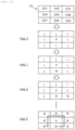
- FIGS. 3 ( a ) and 3 ( b ) are schematic diagrams illustrating an arrangement configuration example of a plurality of channels, and an example of a test pattern thereof.
- FIG. 4 is a schematic diagram illustrating a configuration example of a main part of an ultrasonic probe corresponding to FIG. 3 ( a ) .
- FIG. 5 is a sequence graph illustrating an example of transmission signals transmitted to the respective channels and an example of current change of an ammeter in FIGS. 3 ( b ) and 4 .
- nine channels CH 1 to CH 9 are arranged in three rows and three columns. As shown in FIG.
- each of the channels CH 1 to CH 9 includes the vibrator 2 and the transmission circuit unit 8 that are similar to those in the case of FIG. 1 .
- the ammeter 6 is connected to the positive high-voltage power source 5 as in the case of FIG. 1 .
- a case where a channel CH 5 is set as an observation channel is assumed.
- a test pattern as shown in FIG. 3 ( b ) is set by using the transmission signals TX for test transmitted to the respective channels shown in FIG. 4 .
- an output level of the transmission circuit 1 of the observation channel CH 5 is set to the “H” level
- output levels of eight channels (adjacent channels) CH 1 to CH 4 and CH 6 to CH 9 arranged adjacent to the observation channel are all set to the “L” level.
- a short circuit current I short flows when only the transmission signal TX of the observation channel CH 5 is at the “H” level, and no short circuit current I short flows when the transmission signal TX of the observation channel CH 5 is at the same “L” level as those of the adjacent channels CH 1 to CH 4 and CH 6 to CH 9 .
- FIG. 6 is a schematic diagram illustrating an example of a test method of an ultrasonic probe using the test pattern shown in FIG. 3 ( b ) .
- FIG. 7 is a flowchart illustrating an example of processing contents at the time of implementing the test method of FIG. 6 in the test process (step S 404 ) of FIG. 24 .
- FIG. 6 illustrates an example in which channels are arranged in 8 (A to H) rows and 10 ( 1 to 10 ) columns. In FIG.
- an inspection device generally uses the transmission signals TX for test to change respective output levels of the transmission circuit units 8 of a plurality of channels, and identifies a channel (that is, a channel to which a stop signal STP is to be input) in which a short circuit failure occurs by detecting change in a power source current flowing through the common power source.
- the inspection device sets setting information 121 (operation availability information for each of the plurality of channels) that is stored in the memory 120 in FIG. 23 .
- the inspection device uses the transmission signal TX for test to set the output level of the observation channel to the “H” level and all the output levels of the other channels including the adjacent channel to the “L” level (step S 102 ). Accordingly, a state, in which a potential difference in the output levels of the transmission circuits 1 is generated between the observation channel and the adjacent channel, is constructed. In this state, the inspection device measures a power source current of the common power source by using the ammeter 6 (step S 103 ), and stores a measurement result thereof (step S 104 ).
- the inspection device determines presence or absence of an unmeasured observation channel (step S 105 ), and when there is an unmeasured observation channel, changes the observation channel such that the unmeasured observation channel is selected and returns the process to processing of step S 102 (step S 106 ). Further, the inspection device repeats the processing of steps S 102 to S 104 until there is no unmeasured observation channel (steps S 105 and S 106 ).
- the observation channel is moved in an order of column 1 row A, column 1 row B . . . column 1 row H, column 2 row A, column 2 row B . . . column 10 row 10 .
- the inspection device executes the flow of FIG. 7
- the self-diagnosis unit 103 of the ultrasonic diagnostic device body 101 executes the flow in FIG. 7 at a stage after the ultrasonic probe PB is connected to the ultrasonic diagnostic device body 101 .
- FIG. 8 is a sequence graph illustrating an example of a measurement result of the power source current based on FIGS. 6 and 7 .
- FIG. 9 is a diagram in which the measurement result in FIG. 8 is mapped.
- FIG. 6 it is assumed that a channel of column 2 row C (C 2 ) and a channel of column 3 row D (D 3 ) are short-circuited, and a channel of column 7 row E (E 7 ) and a channel of column 8 row E (E 8 ) are short-circuited.
- a power source current measured by the ammeter 6 exceeds a predetermined current threshold Ith.
- the current threshold Ith can be determined, for example, by converting a predetermined short circuit resistance threshold into a current based on Expression (1).
- the inspection device compares the measured power source current with the current threshold Ith for each observation channel, determines an observation channel (C 2 , D 3 , E 7 and E 8 in this example) with a power source current exceeding the current threshold Ith as a short-circuited channel, and as shown in FIG. 9 , maps the short-circuited channel into a two-dimensional pattern. As a result, the inspection device (or a user thereof) can recognize that a short circuit occurs in the channels adjacent to each other, as indicated by reference numerals 20 .
- FIG. 10 is a schematic diagram illustrating a configuration example of the control circuit in FIG. 1 .
- a short-circuited channel is identified as illustrated in FIGS. 8 and 9 , an operation of the short-circuited channel is stopped, and the ultrasonic probe PB including the short-circuited channel can be regarded as a non-defective product.
- the inspection device determines whether the number of short-circuited channels with respect to a total number of channels is equal to or less than a predetermined ratio (for example, several percent), or whether an occurrence density of the short-circuited channels for each predetermined region is equal to or less than a predetermined density.
- a predetermined ratio for example, several percent
- the inspection device determines an ultrasonic probe PB as a non-defective product in a case where the number of the short-circuited channels is equal to or less than the predetermined ratio or in a case where the occurrence density of the short-circuited channels is equal to or less than the predetermined density, and determines the ultrasonic probe PB as a defective product in other cases.
- a method of stopping the operation of the short-circuited channel in an ultrasonic probe PB that is determined as a non-defective product will be described.
- the control circuit 9 shown in FIG. 10 includes a stop signal holding circuit 30 and an operation determination circuit 31 .
- the stop signal holding circuit 30 holds a stop signal STP (in other words, operation availability information) when the stop signal STP is input in advance.
- the stop signal holding circuit 30 outputs the held stop signal STP to the operation determination circuit 31 in response to an enable signal EN.
- the enable signal EN is issued at a stage when input of the stop signals STP to all the short-circuited channels is completed.
- the operation determination circuit 31 selects whether or not to change the output in response to the transmission signals TX, based on the output from the stop signal holding circuit 30 (that is, based on presence and absence of held stop signal STP).
- FIG. 11 is a circuit diagram illustrating a detailed configuration example of the control circuit of FIG. 10 .
- FIG. 12 is a sequence graph illustrating an operation example of the control circuit of FIG. 11 .
- a row selection signal X_ON [n] a column selection signal Y_ON [m]
- a transmission ON signal TX_ON are input into the stop signal holding circuit 30 as the stop signals STP.
- the row selection signal X_ON [n] and the column selection signal Y_ON [m] are input from the row peripheral circuit 115 and the column peripheral circuit 116 in FIG. 23 , respectively.
- the transmission ON signal TX_ON is commonly input into all the channels.
- the channel to which the stop signal STP is to be input is determined according to the row selection signal X_ON [n] and the column selection signal Y_ON [m]. That is, by setting one of n row selection signals and one of m column selection signals to the “H” level, one corresponding channel is selected.
- the “H” level is input into data input (D) of a flip-flop 43 via an AND operational circuit 41 .
- the column selection signal Y_ON [m] is input into another AND operational circuit 42 , and an inverted signal of the transmission ON signal TX_ON is further input into the AND operational circuit 42 .
- An output of the AND operational circuit 42 is at the “L” level when the transmission ON signal TX_ON is at the “H” level, and is at the “H” level when the transmission ON signal TX_ON is at the “L” level. Therefore, when the transmission ON signal TX_ON is changed from the “H” level to the “L” level, the output of the AND operational circuit 42 is shifted from the “L” level to the “H” level, which is a clock input (CK) of the flip-flop 43 .
- the flip-flop 43 holds the data input (D) at a rising edge of the clock input (CK) and transmits the data input (D) to output (Q).
- n channels corresponding to the column selection signal Y_ON [m] are selected by first controlling one column selection signal Y_ON [m] to be at the “H” level. Further, by controlling a single or a plurality of row selection signals X_ON [n] to be at the “H” level, a single or a plurality of channels corresponding to the short-circuited channel are selected from the n channels. Further, by changing the transmission ON signal TX_ON from the “H” level to the “L” level in a selection period, the output (Q) of the flip-flop 43 of the short-circuited channel is set to the “H” level.
- the output (Q) of the flip-flop 43 is set to the “L” level since the row selection signal X_ON [n] is at the “L” level.
- the clock input (CK) to the flip-flop 43 is not performed since the column selection signal Y_ON [m] is at the “L” level. Therefore, by performing such processing while sequentially setting the column selection signal Y_ON [m] corresponding to a presence part of the short-circuited channel to the “H” level, it is possible to hold the stop signal STP only in the short-circuited channel.
- the AND operational circuit 44 outputs an output of the flip-flop 43 to the operation determination circuit 31 when the enable signal EN is at the “H” level.
- the operation determination circuit 31 for example, outputs the “L” level regardless of the transmission signal TX when the output of the AND operational circuit 44 , which is an AND operational circuit, is at the “H” level, and outputs the transmission signal TX when the output of the AND operational circuit 44 is at the “L” level. Accordingly, when the stop signal holding circuit 30 holds the stop signal STP (that is, when the output of the AND operational circuit 44 is of the “H” level), the output of the control circuit 9 can be fixed to the “L” level, and an operation of a channel can be stopped.
- the inspection device identifies a short-circuited channel through the flow of FIG. 7 , and writes information on the short-circuited channel (that is, the setting information 121 in FIG. 23 ) into the memory 120 of FIG. 23 .
- the ultrasonic diagnostic device body 101 supplies power to the ultrasonic probe PB when the ultrasonic probe PB is connected, and thereafter reads the setting information 121 from the memory 120 of the ultrasonic probe PB.
- the information on the short-circuited channel (that is, the setting information 121 in FIG. 23 ) is written into the memory 120 of FIG. 23
- the following method may be used. That is, the information on the short-circuited channel may be written into a nonvolatile memory provided in the ultrasonic probe PB (not shown), and at the time of actual use, the ultrasonic diagnostic device body 101 may read the information on the short-circuited channel and write the information on the short-circuited channel into the memory 120 of the ultrasonic probe PB.
- the ultrasonic diagnostic device body 101 issues an instruction to the ultrasonic probe PB.
- the instruction is for inputting a stop signal STP to a channel serving as an input target of the stop signal STP.
- the ultrasonic diagnostic device body 101 outputs, for example, an address signal for identifying a channel to be an input target of a stop signal STP, a transmission on signal TX_ON, and an enable signal EN to the ultrasonic probe PB.
- the transmission ON signal TX_ON and the enable signal EN are commonly transmitted to the control circuits 9 of all the channels.
- the address signal is input into the row peripheral circuit 115 and the column peripheral circuit 116 of FIG. 23 .
- the row peripheral circuit 115 and the column peripheral circuit 116 assert a row selection signal X_ON [n] and a column selection signal Y_ON [m], which are corresponding to the address signal, to the “H” level, respectively. Accordingly, a sequence as shown in FIG. 12 is executed. After all the input of the stop signal STP is completed, the ultrasonic diagnostic device body 101 outputs the enable signal EN.
- the self-diagnosis unit 103 executes the flow of FIG. 7 installed on a program in advance, for example, at the time of activation of the ultrasonic diagnostic device 100 or when instructed by a user. Further, when a channel serving as an input target of a stop signal STP is identified through the flow of FIG. 7 , the self-diagnosis unit 103 issues an instruction to the ultrasonic probe PB. The instruction is for inputting the stop signal STP to the identified channel.
- the row selection signal X_ON [n] and the column selection signal Y_ON [m] are used.
- Wiring lines (for example, address wiring lines) of the row selection signal X_ON [n] and the column selection signal Y_ON [m] are originally provided to control each channel during normal operation. Therefore, two wiring lines corresponding to the transmission ON signal TX_ON and the enable signal EN may be added substantially to the control IC 106 .
- an ultrasonic probe PB that is originally defective can be regarded as a non-defective product, so that a defective product rate can be reduced.
- the self-diagnosis unit 103 in the ultrasonic diagnostic device body 101 , it is also possible to relieve product defect of the ultrasonic probe PB due to temporal degradation or the like.
- an application example to a 2D probe is illustrated here, it is needless to say that application to a 1D probe or the like is also possible.
- FIG. 13 is a schematic diagram illustrating an example of the test method for an ultrasonic probe according to the second embodiment of the invention.
- channels CH 1 to CH 9 are arranged in three rows and three columns, and a channel CH 5 among the channels CH 1 to CH 9 is an observation channel.
- the test method is executed by an inspection device or the self-diagnosis unit 103 in the same manner as in the first embodiment, here, a case where the test method is executed by the inspection device is taken as an example.
- the inspection device controls the observation channel CH 5 to an “H” level and the other adjacent channels CH 1 to CH 4 and CH 6 to CH 9 to an “L” level.
- a short circuit current flows as described in the first embodiment.
- the inspection device changes the adjacent channels one by one from the “L” level to the “H” level.
- the channel CH 8 is changed to the “H” level
- the channel CH 9 is changed to the “H” level.
- FIG. 14 is a sequence graph illustrating examples of current change of an ammeter in a case where the test method of FIG. 13 is used.
- a case where a short circuit failure occurs between the observation channel CH 5 and the adjacent channel CH 9 is considered as case 1 .
- Step 0 when the observation channel CH 5 is at the “H” level and the adjacent channels CH 1 to CH 4 and CH 6 to CH 9 are at the “L” level, a short circuit current flows.
- Step 2 since logic of the observation channel CH 5 and that of the adjacent channel CH 9 are equal at a stage where the adjacent channel CH 9 is changed from the “L” level to the “H” level, no short circuit current flows. As a result, the adjacent channel CH 9 can be detected as a short-circuited channel.
- case 2 A case where a short circuit failure occurs between the observation channel CH 5 and the adjacent channel CH 7 is considered as case 2 .
- case 8 since the logic of the observation channel CH 5 and that of the adjacent channel CH 7 are equal at a stage where the adjacent channel CH 7 is changed from the “L” level to the “H” level, no short circuit current flows. As a result, the adjacent channel CH 7 can be detected as a short-circuited channel.
- case 3 A case where short circuit failures occur at two parts, between the observation channel CH 5 and the adjacent channel CH 7 , and between the observation channel CH 5 and the adjacent channel CH 9 , is considered as case 3 .
- the short circuit current is not zero but at an intermediate level determined by a ratio of short circuit resistance.
- the short circuit current is zero.
- FIG. 15 is a flowchart illustrating an example of processing contents at the time when the test method in FIG. 13 is implemented in the test process (step S 404 ) in FIG. 24 .
- the inspection device first sets an output level of the transmission circuit 1 of the observation channel to the “H” level, and sets output levels of the transmission circuits 1 of the other channels to the “L” level (step S 201 ). Subsequently, the inspection device measures the power source current using the ammeter 6 (step S 202 ).
- the inspection device selects one of the adjacent channels, changes an output level of the transmission circuit 1 thereof from the “L” level to the “H” level (step S 203 ), and measures the power source current (step S 204 ). Thereafter, the inspection device repeats the processing of steps S 203 and S 204 until there is no adjacent channel (step S 205 ).
- an order in which the adjacent channels are changed from the “L” level to the “H” level is counterclockwise, it is needless to say that the invention is not limited thereto, and other orders may be used.
- operation stop processing is performed using the method described in the first embodiment.
- the inspection device searches for the adjacent channel between which and the observation channel a short circuit failure occurs, while changing the adjacent channels, between which and the observation channel a potential difference is generated, one by one with the observation channel as reference. Accordingly, in addition to obtaining various effects similar to those of the first embodiment, it is possible to detect a short circuit failure between the observation channel and the adjacent channel without performing mapping. That is, for example, the power source current may exceed a current threshold due to a factor other than a short circuit failure between adjacent channels. In this case, the ultrasonic probe PB may not be regarded as a non-defective product. When the method of the second embodiment is used, differentiation thereof can be directly performed.
- FIG. 16 is a schematic diagram illustrating an example of the test method for an ultrasonic probe according to the third embodiment of the invention.
- a case where a test is performed on channels of eight rows (A to H) and ten columns ( 1 to 10 ) is taken as an example.
- the test method is executed by an inspection device or the self-diagnosis unit 103 in the same manner as in the first embodiment, here, a case where the test method is executed by the inspection device is taken as an example.
- Step 1 the inspection device, taking eight channels (rows A to H) of the same column as observation channels, measures a power source current in a state where output levels of the transmission circuits 1 thereof are controlled to be at an “H” level and all output levels of the other channels are controlled to be at an “L” level. Further, while the inspection device moves the observation channels column by column in units of the observation channels (that is, eight channels arranged in the same column), the inspection device controls output level of each channel to be the same, and measures the power source current each time the observation channels are moved.
- the inspection device taking ten channels (columns 1 to 10 ) of the same row as observation channels, measures the power source current in a state where output levels of the transmission circuits 1 thereof are controlled to be the “H” level and all output levels of the other channels are controlled to be the “L” level. Further, the inspection device moves the observation channels row by row in units of the observation channels (that is, ten channels arranged in the same row), while the inspection device controls output level of each channel to be the same, and measures the power source current each time the observation channels are moved.
- FIG. 17 is a schematic diagram illustrating an example of a test method in a case where there is a short-circuited channel in FIG. 16 .
- a case where a channel of row F column 3 (F 3 ) and a channel of row F column 4 (F 4 ) are short-circuited channels will be described as an example.
- Step 1 when measurement of the power source current is performed while the observation channel is being moved in units of columns from the first column, a short circuit current flows when the observation channels are those in the third column (that is, when each channel in the third column is of the “H” level and the other channels are of the “L” level). Accordingly, it is determined that there is a short-circuited channel in the third column.
- the inspection device measures the current current while changing the eight channels (rows A to H) present in the third column from the “H” level to the “L” level one by one. At this time, when the channel of row F is changed to the “L” level, no short circuit current flows. Accordingly, it is determined that the channel of “F 3 ” is a short-circuited channel. Thereafter, in “Step 1 - 3 ”, if the short-circuited channel identifying processing described in the second embodiment is performed using the channel of “F 3 ” as the observation channel, it is determined that a short circuit failure occurs between the channel of “F 3 ” and the channel of “F 4 ”.
- FIG. 18 is a flowchart illustrating an example of processing contents at the time when the test methods of FIGS. 16 and 17 are implemented in the test process (step S 404 ) in FIG. 24 .
- the inspection device first selects a column to be set as an observation channel (step S 301 ). Subsequently, the inspection device sets output levels of the transmission circuits 1 of the selected observation channel column to the “H” level and output levels of the other channels to the “L” level (step S 302 ), and measures the power source current using the ammeter 6 in this state (step S 303 ).
- the inspection device determines presence or absence of a short circuit failure based on a measurement result of the power source current (step S 304 ).
- the inspection device shifts the process to step S 310 , and when there is a short circuit failure, the inspection device shifts the process to step S 305 .
- the inspection device changes row n of a target column, in which a short circuit failure is detected, to the “L” level in step S 305 , and in this state, measures the current current in step S 306 .
- the inspection device adds the row (n) to be changed to the “L” level (step S 308 ), and repeats the processing of steps S 305 and S 306 (step S 307 ).
- step S 307 when there is change in the measurement result of the current current in step S 307 , the inspection device executes the short-circuited channel identifying processing shown in FIG. 15 , taking the row n of the target column as the observation channel (step S 309 ). Thereafter, in step S 310 , the inspection device determines presence and absence of an unmeasured column, and when there is an unmeasured column, the inspection device repeats executing the processing of steps S 301 to S 309 while moving the column (step S 311 ).
- step S 310 when there is no unmeasured column in step S 310 , the inspection device executes processing similar to that in steps S 301 to S 310 , taking a row as observation channel instead of a column (steps S 401 to S 410 ).
- test is performed first in units of columns, it is needless to say that the test may be performed first in units of rows.
- the specific method of the short-circuited channel identifying processing in steps S 309 and S 409 is not limited to that shown in FIG. 15 , and alternatively other methods may be used.
- operation stop processing is performed using the method described in the first embodiment.
- FIG. 19 is a schematic diagram illustrating an example of a test method for an ultrasonic probe according to a fourth embodiment of the invention.
- a case where a test is performed on channels of eight rows (A to H) and ten columns ( 1 to 10 ) is taken as an example.
- the test method is executed by an inspection device or the self-diagnosis unit 103 in a similar manner as in the first embodiment, here, a case where the test method is executed by the inspection device is taken as an example.
- the inspection device measures a current current while controlling an output level of the transmission circuit 1 , in units of a plurality of channels arranged in a staggered pattern.
- the inspection device divides all the channels into units UT, with four channels adjacent in a row direction and a column direction as one unit UT. Further, as illustrated in “Step 1 ”, the inspection device, controls an output level of one specific channel in the unit UT to be an “H” level and all the other channels to be an “L” level, and measures the current current in a state where the entire channel is set in a test pattern of a staggered pattern. Thereafter, in “Step 2 ” to “Step 4 ”, the inspection device measures the current current while changing clockwise the channel in the unit UT to be the one specific channel. Accordingly, when there is no short-circuited channel, the test can be completed by performing measurement of the current current four times.
- FIG. 20 is a schematic diagram illustrating an example of the test method in a case where there is a short-circuited channel in FIG. 19 .
- a short circuit failure occurs between a channel of row D column 3 (D 3 ) and a channel of row E column 2 (E 2 ).
- E 2 row E column 2
- the inspection device measures the power source current in a state where only one unit UT in the entire channel is set to a logic level of “Step 2 ”. Further, the inspection device measures the current current while sequentially moving the single unit UT in a column direction (or a row direction). As a result, the inspection device detects a short circuit current when the current current is measured at a unit UT including the channel of “D 3 ”, and thus can identify the channel of “D 3 ” as a short-circuited channel.
- the inspection device can identify the channel of “E 2 ” as another short-circuited channel by executing the short-circuited channel identifying processing of FIG. 15 , taking the channel of “D 3 ” as the observation channel.
- operation stop processing is performed using the method described in the first embodiment.
- FIG. 21 is a schematic diagram illustrating an example of a test method for an ultrasonic probe according to a fifth embodiment of the invention.
- a case where a test is performed on channels of eight rows (A to H) and ten columns ( 1 to 10 ) is taken as an example.
- the test method is executed by an inspection device or the self-diagnosis unit 103 in the same manner as in the first embodiment, here, a case where the test method is executed by the inspection device is taken as an example.
- the inspection device measures a current current in a state where an output level of each channel located in an odd-numbered column is set to an “H” level and an output level of each channel located in an even-numbered column is set to an “L” level.
- the inspection device measures the current current in a state where the output level of each channel located in the even-numbered column is set to the “H” level and the output level of each channel located in the odd-numbered column is set to the “L” level.
- Step 2 - 2 the inspection device measures the current current in a state where the output level of each channel located in an even-numbered row is set to the “H” level and the output level of each channel located in an odd-numbered row is set to the “L” level. Subsequently, in “Step 2 - 2 ”, the inspection device measures the current current in a state where the output level of each channel located in the even-numbered row is set to the “H” level and the output level of each channel located in the odd-numbered row is set to the “L” level.
- the test can be completed by performing measurement of the current current four times.
- a short circuit current is detected, for example, it is possible to identify the short-circuited channel by using the same method as that in the case of FIG. 17 .
- a short-circuited channel may be identified, with either the odd-numbered column (odd-numbered row) or even-numbered column (even-numbered row) as target.
- operation stop processing is performed using the method described in the first embodiment.
- the ultrasonic diagnostic device body 101 reads the setting information 121 from the memory 120 of the ultrasonic probe PB, and issues an instruction to the ultrasonic probe PB based on the setting information 121 .
- the instruction is for inputting a stop signal STP to a channel serving as an input target of the stop signal STP.
- the ultrasonic probe PB itself reads the setting information 121 from the memory 120 and inputs the stop signal STP to the transmission circuit 1 of the ultrasonic probe PB based on the read setting information 121 .
Landscapes
- Health & Medical Sciences (AREA)
- Life Sciences & Earth Sciences (AREA)
- Physics & Mathematics (AREA)
- General Health & Medical Sciences (AREA)
- Pathology (AREA)
- General Physics & Mathematics (AREA)
- Chemical & Material Sciences (AREA)
- Analytical Chemistry (AREA)
- Biochemistry (AREA)
- Immunology (AREA)
- Biophysics (AREA)
- Nuclear Medicine, Radiotherapy & Molecular Imaging (AREA)
- Radiology & Medical Imaging (AREA)
- Engineering & Computer Science (AREA)
- Biomedical Technology (AREA)
- Heart & Thoracic Surgery (AREA)
- Medical Informatics (AREA)
- Molecular Biology (AREA)
- Surgery (AREA)
- Animal Behavior & Ethology (AREA)
- Public Health (AREA)
- Veterinary Medicine (AREA)
- Ultra Sonic Daignosis Equipment (AREA)
Abstract
Description
R short =I short/(V OH −V OL) (1)
- 1 transmission circuit
- 2 vibrator
- 5 positive high-voltage power source
- 6 ammeter
- 7 negative high-voltage power source
- 8 transmission circuit unit
- 9 control circuit
- 30 stop signal holding circuit
- 101 ultrasonic diagnostic device
- 103 self-diagnosis unit
- 105 cable
- 106 control IC
- 120 memory
- 121 setting information
- CH channel
- LN wiring line
- PB ultrasonic probe
- STP stop signal
- TX transmission signal
- VU transducer unit
Claims (4)
Applications Claiming Priority (3)
| Application Number | Priority Date | Filing Date | Title |
|---|---|---|---|
| JP2019054886A JP7105207B2 (en) | 2019-03-22 | 2019-03-22 | Ultrasonic probe, ultrasonic diagnostic apparatus, and method for manufacturing ultrasonic probe |
| JP2019-054886 | 2019-03-22 | ||
| JPJP2019-054886 | 2019-03-22 |
Publications (2)
| Publication Number | Publication Date |
|---|---|
| US20200300817A1 US20200300817A1 (en) | 2020-09-24 |
| US11564665B2 true US11564665B2 (en) | 2023-01-31 |
Family
ID=72513642
Family Applications (1)
| Application Number | Title | Priority Date | Filing Date |
|---|---|---|---|
| US16/801,355 Active 2041-06-05 US11564665B2 (en) | 2019-03-22 | 2020-02-26 | Ultrasonic probe, ultrasonic diagnostic device, and manufacturing method of ultrasonic probe |
Country Status (2)
| Country | Link |
|---|---|
| US (1) | US11564665B2 (en) |
| JP (1) | JP7105207B2 (en) |
Families Citing this family (2)
| Publication number | Priority date | Publication date | Assignee | Title |
|---|---|---|---|---|
| KR102888556B1 (en) * | 2020-03-24 | 2025-11-21 | 삼성메디슨 주식회사 | Ultrasonic probe, ultrasonic imaging device and controlling method thereof |
| US20250244208A1 (en) * | 2024-01-30 | 2025-07-31 | Saudi Arabian Oil Company | Method and apparatus for testing the health of a proximity vibration sensory loop |
Citations (15)
| Publication number | Priority date | Publication date | Assignee | Title |
|---|---|---|---|---|
| US5027821A (en) * | 1988-06-17 | 1991-07-02 | Kabushiki Kaisha Toshiba | Ultrasonic imaging apparatus |
| US6225729B1 (en) * | 1997-12-01 | 2001-05-01 | Hitachi Medical Corporation | Ultrasonic probe and ultrasonic diagnostic apparatus using the probe |
| JP2002159492A (en) | 2000-11-27 | 2002-06-04 | Aloka Co Ltd | Ultrasonic diagnostic equipment and element testing method |
| JP2004174227A (en) | 2002-09-30 | 2004-06-24 | Fuji Photo Film Co Ltd | Ultrasonic search unit and ultrasonic transmitter/receiver using the same |
| JP2004229979A (en) | 2003-01-31 | 2004-08-19 | Aloka Co Ltd | Ultrasonic diagnostic apparatus and ultrasonic probe |
| US20060145059A1 (en) | 2005-01-04 | 2006-07-06 | Warren Lee | Isolation of short-circuited sensor cells for high-reliability operation of sensor array |
| US20080225639A1 (en) | 2007-03-14 | 2008-09-18 | Kabushiki Kaisha Toshiba | Ultrasonic imaging apparatus |
| JP2009261611A (en) | 2008-04-24 | 2009-11-12 | Konica Minolta Medical & Graphic Inc | Ultrasonic diagnostic apparatus and method |
| US7766838B2 (en) * | 2002-04-17 | 2010-08-03 | Hitachi Medical Corporation | Ultrasonic probe in body cavity |
| US8727994B2 (en) * | 2010-12-14 | 2014-05-20 | Samsung Electronics Co., Ltd. | Cell and channel of ultrasonic transducer, and ultrasonic transducer including the same |
| US20150157299A1 (en) | 2013-12-06 | 2015-06-11 | Siemens Medical Solutions Usa, Inc. | Sub-performing transducer element detection for medical ultrasound |
| US9089874B2 (en) * | 2007-12-13 | 2015-07-28 | Hitachi Medical Corporation | Ultrasonic diagnostic apparatus and ultrasonic probe |
| US20170176581A1 (en) | 2015-12-21 | 2017-06-22 | Samsung Electronics Co., Ltd. | Ultrasonic image apparatus and control method thereof |
| JP2018068363A (en) | 2016-10-24 | 2018-05-10 | キヤノン株式会社 | Ultrasonic probe and subject information acquisition apparatus using the same |
| US10390794B2 (en) * | 2012-08-07 | 2019-08-27 | Canon Medical Systems Corporation | Ultrasound diagnostic apparatus and ultrasound probe |
-
2019
- 2019-03-22 JP JP2019054886A patent/JP7105207B2/en active Active
-
2020
- 2020-02-26 US US16/801,355 patent/US11564665B2/en active Active
Patent Citations (18)
| Publication number | Priority date | Publication date | Assignee | Title |
|---|---|---|---|---|
| US5027821A (en) * | 1988-06-17 | 1991-07-02 | Kabushiki Kaisha Toshiba | Ultrasonic imaging apparatus |
| US6225729B1 (en) * | 1997-12-01 | 2001-05-01 | Hitachi Medical Corporation | Ultrasonic probe and ultrasonic diagnostic apparatus using the probe |
| JP2002159492A (en) | 2000-11-27 | 2002-06-04 | Aloka Co Ltd | Ultrasonic diagnostic equipment and element testing method |
| US7766838B2 (en) * | 2002-04-17 | 2010-08-03 | Hitachi Medical Corporation | Ultrasonic probe in body cavity |
| JP2004174227A (en) | 2002-09-30 | 2004-06-24 | Fuji Photo Film Co Ltd | Ultrasonic search unit and ultrasonic transmitter/receiver using the same |
| US20040220463A1 (en) | 2002-09-30 | 2004-11-04 | Fuji Photo Film Co., Ltd. | Ultrasonic probe and ultrasonic transmitting and receiving apparatus using the same |
| JP2004229979A (en) | 2003-01-31 | 2004-08-19 | Aloka Co Ltd | Ultrasonic diagnostic apparatus and ultrasonic probe |
| US20060145059A1 (en) | 2005-01-04 | 2006-07-06 | Warren Lee | Isolation of short-circuited sensor cells for high-reliability operation of sensor array |
| JP2006343315A (en) | 2005-01-04 | 2006-12-21 | General Electric Co <Ge> | Isolation of shorted sensor cells for reliable operation of sensor arrays |
| US20080225639A1 (en) | 2007-03-14 | 2008-09-18 | Kabushiki Kaisha Toshiba | Ultrasonic imaging apparatus |
| JP2008220753A (en) | 2007-03-14 | 2008-09-25 | Toshiba Corp | Ultrasonic diagnostic apparatus and ultrasonic probe |
| US9089874B2 (en) * | 2007-12-13 | 2015-07-28 | Hitachi Medical Corporation | Ultrasonic diagnostic apparatus and ultrasonic probe |
| JP2009261611A (en) | 2008-04-24 | 2009-11-12 | Konica Minolta Medical & Graphic Inc | Ultrasonic diagnostic apparatus and method |
| US8727994B2 (en) * | 2010-12-14 | 2014-05-20 | Samsung Electronics Co., Ltd. | Cell and channel of ultrasonic transducer, and ultrasonic transducer including the same |
| US10390794B2 (en) * | 2012-08-07 | 2019-08-27 | Canon Medical Systems Corporation | Ultrasound diagnostic apparatus and ultrasound probe |
| US20150157299A1 (en) | 2013-12-06 | 2015-06-11 | Siemens Medical Solutions Usa, Inc. | Sub-performing transducer element detection for medical ultrasound |
| US20170176581A1 (en) | 2015-12-21 | 2017-06-22 | Samsung Electronics Co., Ltd. | Ultrasonic image apparatus and control method thereof |
| JP2018068363A (en) | 2016-10-24 | 2018-05-10 | キヤノン株式会社 | Ultrasonic probe and subject information acquisition apparatus using the same |
Non-Patent Citations (1)
| Title |
|---|
| Japanese-language Office Action issued in Japanese Application No. 2019-054886 dated Mar. 15, 2022 with English translation (eight (8) pages). |
Also Published As
| Publication number | Publication date |
|---|---|
| JP2020151350A (en) | 2020-09-24 |
| US20200300817A1 (en) | 2020-09-24 |
| JP7105207B2 (en) | 2022-07-22 |
Similar Documents
| Publication | Publication Date | Title |
|---|---|---|
| US10969432B2 (en) | System-on-chip for at-speed test of logic circuit and operating method thereof | |
| US20180364303A1 (en) | Apparatuses including test segment circuits and methods for testing the same | |
| US11564665B2 (en) | Ultrasonic probe, ultrasonic diagnostic device, and manufacturing method of ultrasonic probe | |
| CN112462353B (en) | Ultrasonic radar testing method, device, system and equipment | |
| US20020039032A1 (en) | Testing method and testing device for semiconductor integrated circuits | |
| US9612276B2 (en) | Test device and test system including the same | |
| US10319865B2 (en) | Pressure detecting apparatus and method of driving the same | |
| US20120163108A1 (en) | Non-volatile memory device and electronic apparatus | |
| EP2829883A1 (en) | Switching loss measurement and plot in test and measurement instrument | |
| CN100578664C (en) | Redundant control circuit and semiconductor storage device using the redundant control circuit | |
| US11422201B1 (en) | Devices and methods for voltage supply monitoring | |
| US7952381B2 (en) | Semiconductor device | |
| JPH1065104A (en) | Semiconductor integrated circuit | |
| WO2023028984A1 (en) | Methods and systems for automatic waveform analysis | |
| US8341477B2 (en) | Test board having a plurality of test modules and a test system having the same | |
| US20210158771A1 (en) | Driving circuit, display module, and mobile body | |
| JPWO2011048723A1 (en) | Semiconductor integrated circuit for driving display panel, driving module for display panel, and display device | |
| US20140077814A1 (en) | Method and system for testing matrices and method for controlling voltage clocks | |
| US7202688B2 (en) | Output buffer circuit having signal path used for testing and integrated circuit and test method including the same | |
| JP2002318551A (en) | Device and method for inspecting pixel of active matrix type display | |
| CN114113971A (en) | Integrated circuit and test method thereof | |
| US7495979B2 (en) | Method and system for in-situ parametric SRAM diagnosis | |
| KR20240031782A (en) | Test board and test method for semiconductor device using the same | |
| CN115808665A (en) | Self-diagnosis method and system of echo amplification circuit, switching method and liquid level gauge | |
| CN114171098A (en) | Abnormal word line testing method and device, memory and memory system |
Legal Events
| Date | Code | Title | Description |
|---|---|---|---|
| AS | Assignment |
Owner name: HITACHI, LTD., JAPAN Free format text: ASSIGNMENT OF ASSIGNORS INTEREST;ASSIGNORS:YAZAKI, TORU;IGARASHI, YUTAKA;HAYASHI, YOSHIHIRO;AND OTHERS;REEL/FRAME:051937/0427 Effective date: 20200212 |
|
| FEPP | Fee payment procedure |
Free format text: ENTITY STATUS SET TO UNDISCOUNTED (ORIGINAL EVENT CODE: BIG.); ENTITY STATUS OF PATENT OWNER: LARGE ENTITY |
|
| STPP | Information on status: patent application and granting procedure in general |
Free format text: APPLICATION DISPATCHED FROM PREEXAM, NOT YET DOCKETED |
|
| STPP | Information on status: patent application and granting procedure in general |
Free format text: DOCKETED NEW CASE - READY FOR EXAMINATION |
|
| AS | Assignment |
Owner name: FUJIFILM HEALTHCARE CORPORATION, JAPAN Free format text: ASSIGNMENT OF ASSIGNORS INTEREST;ASSIGNOR:HITACHI, LTD.;REEL/FRAME:058472/0063 Effective date: 20211203 |
|
| STPP | Information on status: patent application and granting procedure in general |
Free format text: NON FINAL ACTION MAILED |
|
| STPP | Information on status: patent application and granting procedure in general |
Free format text: RESPONSE TO NON-FINAL OFFICE ACTION ENTERED AND FORWARDED TO EXAMINER |
|
| STPP | Information on status: patent application and granting procedure in general |
Free format text: NOTICE OF ALLOWANCE MAILED -- APPLICATION RECEIVED IN OFFICE OF PUBLICATIONS |
|
| STPP | Information on status: patent application and granting procedure in general |
Free format text: PUBLICATIONS -- ISSUE FEE PAYMENT VERIFIED |
|
| STCF | Information on status: patent grant |
Free format text: PATENTED CASE |
|
| AS | Assignment |
Owner name: FUJIFILM CORPORATION, JAPAN Free format text: MERGER;ASSIGNOR:FUJIFILM HEALTHCARE CORPORATION;REEL/FRAME:070607/0722 Effective date: 20240701 |
|
| AS | Assignment |
Owner name: FUJIFILM CORPORATION, JAPAN Free format text: MERGER;ASSIGNOR:FUJIFILM HEALTHCARE CORPORATION;REEL/FRAME:069818/0566 Effective date: 20240701 |