US11544838B2 - Systems and methods of high-resolution review for semiconductor inspection in backend and wafer level packaging - Google Patents
Systems and methods of high-resolution review for semiconductor inspection in backend and wafer level packaging Download PDFInfo
- Publication number
- US11544838B2 US11544838B2 US16/826,193 US202016826193A US11544838B2 US 11544838 B2 US11544838 B2 US 11544838B2 US 202016826193 A US202016826193 A US 202016826193A US 11544838 B2 US11544838 B2 US 11544838B2
- Authority
- US
- United States
- Prior art keywords
- light
- sample
- image
- light source
- processor
- Prior art date
- Legal status (The legal status is an assumption and is not a legal conclusion. Google has not performed a legal analysis and makes no representation as to the accuracy of the status listed.)
- Active, expires
Links
Images


Classifications
-
- G—PHYSICS
- G01—MEASURING; TESTING
- G01N—INVESTIGATING OR ANALYSING MATERIALS BY DETERMINING THEIR CHEMICAL OR PHYSICAL PROPERTIES
- G01N21/00—Investigating or analysing materials by the use of optical means, i.e. using sub-millimetre waves, infrared, visible or ultraviolet light
- G01N21/84—Systems specially adapted for particular applications
- G01N21/88—Investigating the presence of flaws or contamination
- G01N21/8806—Specially adapted optical and illumination features
-
- G—PHYSICS
- G01—MEASURING; TESTING
- G01N—INVESTIGATING OR ANALYSING MATERIALS BY DETERMINING THEIR CHEMICAL OR PHYSICAL PROPERTIES
- G01N21/00—Investigating or analysing materials by the use of optical means, i.e. using sub-millimetre waves, infrared, visible or ultraviolet light
- G01N21/84—Systems specially adapted for particular applications
- G01N21/88—Investigating the presence of flaws or contamination
- G01N21/95—Investigating the presence of flaws or contamination characterised by the material or shape of the object to be examined
- G01N21/9501—Semiconductor wafers
-
- G—PHYSICS
- G01—MEASURING; TESTING
- G01N—INVESTIGATING OR ANALYSING MATERIALS BY DETERMINING THEIR CHEMICAL OR PHYSICAL PROPERTIES
- G01N21/00—Investigating or analysing materials by the use of optical means, i.e. using sub-millimetre waves, infrared, visible or ultraviolet light
- G01N21/84—Systems specially adapted for particular applications
- G01N21/88—Investigating the presence of flaws or contamination
- G01N21/95—Investigating the presence of flaws or contamination characterised by the material or shape of the object to be examined
- G01N21/956—Inspecting patterns on the surface of objects
- G01N21/95684—Patterns showing highly reflecting parts, e.g. metallic elements
-
- G—PHYSICS
- G02—OPTICS
- G02B—OPTICAL ELEMENTS, SYSTEMS OR APPARATUS
- G02B21/00—Microscopes
- G02B21/06—Means for illuminating specimens
- G02B21/08—Condensers
- G02B21/14—Condensers affording illumination for phase-contrast observation
-
- G—PHYSICS
- G02—OPTICS
- G02B—OPTICAL ELEMENTS, SYSTEMS OR APPARATUS
- G02B21/00—Microscopes
- G02B21/16—Microscopes adapted for ultraviolet illumination ; Fluorescence microscopes
-
- G—PHYSICS
- G02—OPTICS
- G02B—OPTICAL ELEMENTS, SYSTEMS OR APPARATUS
- G02B21/00—Microscopes
- G02B21/33—Immersion oils, or microscope systems or objectives for use with immersion fluids
-
- G—PHYSICS
- G02—OPTICS
- G02B—OPTICAL ELEMENTS, SYSTEMS OR APPARATUS
- G02B21/00—Microscopes
- G02B21/36—Microscopes arranged for photographic purposes or projection purposes or digital imaging or video purposes including associated control and data processing arrangements
- G02B21/365—Control or image processing arrangements for digital or video microscopes
- G02B21/367—Control or image processing arrangements for digital or video microscopes providing an output produced by processing a plurality of individual source images, e.g. image tiling, montage, composite images, depth sectioning, image comparison
-
- G—PHYSICS
- G06—COMPUTING OR CALCULATING; COUNTING
- G06T—IMAGE DATA PROCESSING OR GENERATION, IN GENERAL
- G06T7/00—Image analysis
- G06T7/0002—Inspection of images, e.g. flaw detection
- G06T7/0004—Industrial image inspection
- G06T7/0006—Industrial image inspection using a design-rule based approach
-
- H01L21/67288—
-
- H—ELECTRICITY
- H10—SEMICONDUCTOR DEVICES; ELECTRIC SOLID-STATE DEVICES NOT OTHERWISE PROVIDED FOR
- H10P—GENERIC PROCESSES OR APPARATUS FOR THE MANUFACTURE OR TREATMENT OF DEVICES COVERED BY CLASS H10
- H10P72/00—Handling or holding of wafers, substrates or devices during manufacture or treatment thereof
- H10P72/06—Apparatus for monitoring, sorting, marking, testing or measuring
- H10P72/0616—Monitoring of warpages, curvatures, damages, defects or the like
-
- H—ELECTRICITY
- H10—SEMICONDUCTOR DEVICES; ELECTRIC SOLID-STATE DEVICES NOT OTHERWISE PROVIDED FOR
- H10P—GENERIC PROCESSES OR APPARATUS FOR THE MANUFACTURE OR TREATMENT OF DEVICES COVERED BY CLASS H10
- H10P74/00—Testing or measuring during manufacture or treatment of wafers, substrates or devices
- H10P74/20—Testing or measuring during manufacture or treatment of wafers, substrates or devices characterised by the properties tested or measured, e.g. structural or electrical properties
- H10P74/203—Structural properties, e.g. testing or measuring thicknesses, line widths, warpage, bond strengths or physical defects
-
- G—PHYSICS
- G01—MEASURING; TESTING
- G01N—INVESTIGATING OR ANALYSING MATERIALS BY DETERMINING THEIR CHEMICAL OR PHYSICAL PROPERTIES
- G01N21/00—Investigating or analysing materials by the use of optical means, i.e. using sub-millimetre waves, infrared, visible or ultraviolet light
- G01N21/84—Systems specially adapted for particular applications
- G01N21/88—Investigating the presence of flaws or contamination
- G01N21/8806—Specially adapted optical and illumination features
- G01N2021/8845—Multiple wavelengths of illumination or detection
-
- G—PHYSICS
- G06—COMPUTING OR CALCULATING; COUNTING
- G06T—IMAGE DATA PROCESSING OR GENERATION, IN GENERAL
- G06T2207/00—Indexing scheme for image analysis or image enhancement
- G06T2207/10—Image acquisition modality
- G06T2207/10141—Special mode during image acquisition
- G06T2207/10152—Varying illumination
-
- G—PHYSICS
- G06—COMPUTING OR CALCULATING; COUNTING
- G06T—IMAGE DATA PROCESSING OR GENERATION, IN GENERAL
- G06T2207/00—Indexing scheme for image analysis or image enhancement
- G06T2207/30—Subject of image; Context of image processing
- G06T2207/30108—Industrial image inspection
- G06T2207/30148—Semiconductor; IC; Wafer
Definitions
- This disclosure relates to wafer defect review.
- WLP backend and wafer level package
- UV visible, ultraviolet
- DUV deep ultraviolet
- DOI defect-of-interest
- NA numerical aperture
- the design rule is shrinking to 1 ⁇ m and the roadmap exists to 0.4 ⁇ m.
- the defect size in such design rules may be 0.2 ⁇ m.
- the previously-mentioned review methods currently cannot, due to physical limitations of wavelength over NA (where NA is limited to be less than or equal to 1.0), provide the image quality needed for detection and classification purposes in such design rules.
- UV or DUV may damage the wafer, so the wavelength may be limited to the visible range.
- SEM Scanning electron microscopy
- a review system is provided in a first embodiment.
- the review system comprises a stage having the sample disposed thereon; a light source configured to emit a beam of light toward the sample; a detector configured to detect a portion of the beam of light reflected by the sample; a plurality of objectives; and a processor in electronic communication with the detector.
- the processor is configured to perform a review of defects on the sample.
- the sample is a wafer level packaging wafer or a backend wafer.
- the review system further includes an immersion subsystem that includes a fluid supply unit and a fluid removal unit; the light source includes a plurality of light-emitting diodes configured to form illumination patterns for differential phase contrast; and/or the light source includes a white light source that emits ultraviolet or deep ultraviolet wavelengths.
- the light source can include the plurality of light-emitting diodes.
- the light-emitting diodes may be colored.
- the light source can include a relay lens.
- the relay lens can be configured to image the beam of light reflected by the sample to the detector through at least one of the objectives.
- the detector can convert the light beam from the relay lens into an image using a frame grabber module.
- the frame grabber module can be synchronized with the stage.
- the light source can be the white light source.
- the light source can further include a color filter and a spatial filter.
- the processor can be further configured to generate an intensity image and a phase image.
- the intensity image and the phase image can be generated as a function of height.
- the processor can be further configured to generate a composite image from the intensity image and the phase image.
- the review system includes the immersion subsystem, the light source is the white light source, and the system includes the plurality of light-emitting diodes.
- An inspection system can include the review system of the first embodiment.
- a method is provided in a second embodiment.
- the method comprises directing a beam of light toward a sample on a stage.
- the sample is a wafer level packaging wafer or a backend wafer.
- the beam of light reflected from the sample is received at a detector.
- a processor Using a processor, a review of defects on the sample is performed.
- One or more of the following also occurs.
- a fluid is supplied between the sample and an optical objective by an immersion subsystem that includes a fluid supply unit.
- an illumination pattern is formed with the beam of light for differential phase contrast.
- the beam of light is at ultraviolet or deep ultraviolet wavelengths.
- the beam of light can be generated by a plurality of light-emitting diodes.
- the light-emitting diodes can be colored.
- the method can include imaging the beam of light reflected by the sample through at least one objective to the detector using a relay lens.
- the beam of light from the relay lens can be converted into an image using a frame grabber module.
- the frame grabber module can be synchronized with the stage.
- the light source can be the white light source.
- the light source further can include a color filter and a spatial filter.
- the method can further include generating, using the processor, an intensity image and a phase image.
- the intensity image and the phase image are generated as a function of height.
- a composite image can be generated from the intensity image and the phase image.
- the method includes the supplying the fluid, forming the illumination pattern for the differential phase contrast, and the beam of light being at the ultraviolet or deep ultraviolet wavelengths.
- FIG. 1 illustrates an embodiment of a system in accordance with the present disclosure
- FIG. 2 illustrates a further embodiment of a system in accordance with the present disclosure.
- FIG. 3 illustrates an embodiment of a method in accordance with the present disclosure.
- the systems and methods disclosed herein can provide review support for aWLP and BE applications.
- embodiments can 1) apply immersion technology to review and classify defects, 2) apply differential phase contrast (DPC) technology to review and classify defects, 3) apply focus scan with DPC technology to review and classify defects, 4) apply polarization control to an illumination source and tube-lens with a quantitative modeling algorithm for DPC, or 5) use one or more of the techniques 1) through 4) with ultraviolet (UV) or deep ultraviolet (DUV) to review and classify defects.
- the system can be configured for different applications. For example, the system can combine DUV and immersion with DPC for one application, visible wavelength with immersion and DPC for another application, and visible wavelength with DPC and focus scan for yet another application. These different applications can be performed in the same review system.
- Use of one or more of the techniques 1) through 4) may depend on the size and material of the defect and/or can involve a balance against the speed of performance. If the defect is large (e.g., 1 ⁇ m) and the material on wafer is DUV compatible, then DUV or immersion DUV may be used. If the defect size is large (e.g., 1 ⁇ m) and the material is UV/DUV incompatible, then immersion vis imaging can be used. If more resolution is needed, DPC may be needed, though this is slightly slower. For small defects (e.g., 0.4 ⁇ m), immersion DUV applied through focus scan DPC can be used. In general, for finding broken/short Cu-lines, DUV and immersion may be more useful. For organic defects on Cu lines/surfaces, the DPC and through focus scan may provide more value.
- the semiconductor industry is moving into 2 ⁇ m. Previously, the defect size was approximately 2 ⁇ m to 5 ⁇ m, and a high NA dry optical microscope met the application requirements. More semiconductor manufacturers are moving move to 2 ⁇ m or less than 2 ⁇ m design rules.
- the embodiments disclosed herein can be used by semiconductor manufacturers that need improved throughput or cannot afford multiple scanning electron microscope steps for such defects.
- Embodiments disclosed herein can be configured for the needs of a semiconductor manufacturer. Performance, speed, and cost can be balanced.
- the system 100 includes optical based subsystem 101 (i.e., an optical review tool).
- the optical based subsystem 101 is configured for generating optical based output for a sample 102 by directing light to (or scanning light over) and detecting light from the sample 102 .
- the sample 102 includes a wafer, constructed wafer, or wafers that are bonded.
- the wafer may include any wafer known in the art, such as an aWLP or BE wafer.
- optical based subsystem 101 includes an illumination subsystem configured to direct light to sample 102 .
- the illumination subsystem includes at least one light source.
- the illumination subsystem includes light source 103 .
- the illumination subsystem is configured to direct the light to the sample 102 at one or more angles of incidence, which may include one or more oblique angles and/or one or more normal angles.
- light from light source 103 is directed through optical element 104 and then lens 105 to sample 102 at an normal angle of incidence.
- the oblique angle of incidence may include any suitable oblique angle of incidence, which may vary depending on, for instance, characteristics of the sample 102 .
- the optical based subsystem 101 may be configured to direct the light to the sample 102 at different angles of incidence at different times.
- the optical based subsystem 101 may be configured to alter one or more characteristics of one or more elements of the illumination subsystem such that the light can be directed to the sample 102 at an angle of incidence that is different from that shown in FIG. 1 .
- the optical based subsystem 101 may be configured to move light source 103 , optical element 104 , lens 105 , and optical objective 110 such that the light is directed to the sample 102 at a different angle of incidence or an oblique (or near normal) angle of incidence.
- An illumination beam at oblique angle of incident also can be done via outside of the objective lens 110 , as shown with optional second light source 116 .
- a scan mechanism can change the distance between the sample 102 and objective lens 110 .
- Various images or other data can be taken at a pre-determined position or positions.
- the optical based subsystem 101 may be configured to direct light to the sample 102 at more than one angle of incidence at the same time.
- the illumination subsystem may include more than one illumination channel.
- One of the illumination channels may include light source 103 , through optical element 104 , and lens 105 as shown in FIG. 1 and another of the illumination channels (not shown) may include similar elements (or not similar lenses such as illuminating outside the objective lens 110 ), which may be configured differently (such as wavelength polarization) or the same, or may include at least a light source and possibly one or more other components such as those described further herein.
- one or more characteristics e.g., wavelength, polarization, etc.
- characteristics e.g., wavelength, polarization, etc.
- the illumination subsystem may include only one light source (e.g., light source 103 shown in FIG. 1 ) and light from the light source may be separated into different optical paths (e.g., based on wavelength, polarization, etc.) by one or more optical elements (not shown) of the illumination subsystem. Light in each of the different optical paths may then be directed to the sample 102 .
- Multiple illumination channels may be configured to direct light to the sample 102 at the same time or at different times (e.g., when different illumination channels are used to sequentially illuminate the specimen). In another instance, the same illumination channel may be configured to direct light to the sample 102 with different characteristics at different times.
- optical element 104 may be configured as a spectral filter and the properties of the spectral filter can be changed in a variety of different ways (e.g., by swapping out the spectral filter) such that different wavelengths of light can be directed to the sample 102 at different times.
- the illumination subsystem may have any other suitable configuration known in the art for directing the light having different or the same characteristics to the sample 102 at different or the same angles of incidence sequentially or simultaneously.
- the system 100 also can include an optional second light source 116 and light conditioning optics 117 .
- the second light source 116 can provide an oblique illumination channel.
- the detection channel is shown positioned in the plane of the paper and the illumination subsystem is also shown positioned in the plane of the paper. Therefore, in this embodiment, the detection channel is positioned in (e.g., centered in) the plane of incidence. However, one or more of the detection channels may be positioned out of the plane of incidence.
- each of the detection channels included in the optical based subsystem 101 may be configured to detect scattered light. Therefore, the optical based subsystem 101 shown in FIG. 1 may be configured for dark field (DF) output generation for specimens 102 . However, the optical based subsystem 101 may also or alternatively include detection channel(s) that are configured for bright field (BF) output generation for specimens 102 . In other words, the optical based subsystem 101 may include at least one detection channel that is configured to detect light specularly reflected from the sample 102 . Therefore, the optical based subsystems 101 described herein may be configured for only DF, only BF, or both DF and BF imaging. Although each of the collectors is shown in FIG. 1 as a single refractive optical element, it is to be understood that each of the collectors may include one or more refractive optical die(s) and/or one or more reflective optical element(s).
- the detector 109 may include charge coupled devices (CCDs), time delay integration (TDI) cameras, and any other suitable detectors known in the art.
- the detector may also include non-imaging detectors or imaging detectors. In this manner, if the detectors with multiple detection channels are non-imaging detectors, each of the detectors may be configured to detect certain characteristics of the scattered light such as intensity but may not be configured to detect such characteristics as a function of position within the imaging plane.
- the output that is generated by each of the detectors included in each of the detection channels of the optical based subsystem may be signals or data, but not image signals or image data.
- a processor such as processor 114 may be configured to generate images of the sample 102 from the non-imaging output of the detectors.
- the detectors may be configured as imaging detectors that are configured to generate imaging signals or image data. Therefore, the optical based subsystem may be configured to generate optical images or other optical based output described herein in a number of ways.
- the light source 103 may include any suitable light source.
- the light source 103 includes multiple light-emitting diodes (LEDs) configured to form an illumination pattern for DPC.
- the LEDs are in a 32 ⁇ 32 array with a discrete grid pattern.
- the LEDs are in a 4-8 ring shape with 16 LEDs in each ring.
- Each LED can be treated as a coherent point source.
- the LEDs can be activated in a radius of a half-circle. The radius of the LED array can vary.
- the light source 103 includes a white light source that emits from visible to UV and DUV wavelengths, such as Xe lamps.
- the light source 103 in this example also can be one or more LEDs.
- the light source 103 can further include a color filter and spatial filter.
- the white light source can provide DUV wavelengths.
- the color filter can be fixed in a wheel or can be a variable filter.
- the spatial filter can be programmable pin-holes or blinks.
- UV LEDs that provide center wavelength around 355 nm or approximately 388 nm.
- Visible LEDs can be 435 nm, 530 nm and 635 nm. Other wavelengths are possible.
- Xe lamps with color filters may be used for DUV.
- the light source 103 includes a plurality of LEDs.
- the LEDs in this example are colored.
- the light source 103 also may include a polarized light source and/or a tube lens.
- the optical based subsystem 101 can have multiple objectives. Some objectives work in dry conditions and other objectives work with immersion using various NA and field of view (FoV). The objectives can be changed or selected for a particular receipt using, for example, a motorized turret, which may be rotational or linear staged.
- a motorized turret which may be rotational or linear staged.
- Lens 105 Light from optical element 104 may be focused onto sample 102 by lens 105 .
- lens 105 is shown in FIG. 1 as a single refractive optical element, it is to be understood that, in practice, lens 105 may include a number of refractive and/or reflective optical elements that in combination focus the light from the optical element to the specimen.
- the illumination subsystem shown in FIG. 1 and described herein may include any other suitable optical elements (not shown). Examples of such optical elements include, but are not limited to, polarizing component(s), spectral filter(s), spatial filter(s), reflective optical element(s), apodizer(s), beam splitter(s) (such as beam splitter 113 ), aperture(s), and the like, which may include any such suitable optical elements known in the art.
- the optical based subsystem 101 may be configured to alter one or more of the elements of the illumination subsystem based on the type of illumination to be used for generating the optical based output.
- the light from the optical element 104 can be imaged on the back focal plane of the objective.
- the images of the light reflected from the sample 102 can be taken with pre-programmed illumination patterns.
- the images of the light reflected from the sample 102 are taken at different relative distance between the sample 102 and the objective 110 .
- the light source 103 (or lens 105 of the illumination subsystem) includes a relay lens (e.g., a tube lens).
- the relay lens can be configured to image the beam of light reflected by the sample through at least one of the objectives to the detector 109 , such as the objective 110 .
- the optical based subsystem 101 may also include a scanning subsystem configured to cause the light to be scanned over the sample 102 .
- the optical based subsystem 101 may include stage 106 on which sample 102 is disposed during optical based output generation.
- the scanning subsystem may include any suitable mechanical and/or robotic assembly (that includes stage 106 ) that can be configured to move the sample 102 such that the light can be scanned over the sample 102 .
- the optical based subsystem 101 may be configured such that one or more optical elements of the optical based subsystem 101 perform some scanning of the light over the sample 102 .
- the light may be scanned over the sample 102 in any suitable fashion such as in a serpentine-like path or in a spiral path.
- the optical based subsystem 101 includes an immersion subsystem 111 , which can include a fluid supply unit and a fluid removal unit.
- a fluid is provided between the sample 102 and the optical objective 110 .
- the fluid may have a refractive index higher than air.
- the fluid may be water, which has a refractive index of approximately 1.4, or another liquid compatible with the sample 102 .
- alcohol or oil may be used as the fluid.
- the fluid has a refractive index greater than 1.5.
- the equivalent NA is larger than 1.0, which can avoid UV or DUV light damage to the sample 102 .
- the system is configured in a way such that there is a clean liquid supplier 118 to the gap (e.g., a needle or nozzle) and a liquid remover 119 (e.g., a vacuum). Additional details are disclosed in U.S. Pat. No. 7,436,527, which is incorporated by reference in its entirety.
- the gap may be the separation distance h depicted in FIG. 2 between the end surface of the optical objective 110 and the surface of the sample 102 .
- the gap may be an air gap or vacuum.
- the fluid 112 occupies the gap between the optical objective 110 and the sample 102 .
- the gap between the optical objective 110 and the sample 102 may be completely filled with air or liquid.
- the fluid is contained in the fluid supply unit of the immersion subsystem 111 .
- the fluid can be pumped to a bottom surface of optical objective 110 .
- Fluid can be is forced through into the volume between the optical objective 110 and the sample 102 using the liquid supplier 118 .
- Residual fluid can be dried off with the liquid remover 119 .
- the liquid can return to the immersion subsystem 111 . Therefore, the system is configured to generate flow of the liquid between the surfaces of the optical objective 110 and the sample 102 during review. Additional details are disclosed in U.S. Pat. No. 7,130,037, which is incorporated by reference in its entirety.
- the light source 103 can include a plurality of light-emitting diodes.
- the light source 103 can be a white light source.
- FIG. 1 is provided herein to generally illustrate a configuration of an optical based subsystem 101 that may be included in the system embodiments described herein or that may generate optical based output that is used by the system embodiments described herein.
- the optical based subsystem 101 configuration described herein may be altered to optimize the performance of the optical based subsystem 101 as is normally performed when designing a commercial output acquisition system.
- the systems described herein may be implemented using an existing system (e.g., by adding functionality described herein to an existing system).
- the methods described herein may be provided as optional functionality of the system (e.g., in addition to other functionality of the system).
- the system described herein may be designed as a completely new system.
- the processor 114 may be coupled to the components of the system 100 in any suitable manner (e.g., by one or more transmission media, which may include wired and/or wireless transmission media) such that the processor 114 can receive output.
- the processor 114 may be configured to perform a number of functions using the output.
- the system 100 can receive instructions or other information from the processor 114 .
- the processor 114 and/or the electronic data storage unit 115 optionally may be in electronic communication with a wafer inspection tool, a wafer metrology tool, or a wafer review tool (not illustrated) to receive additional information or send instructions.
- the processor 114 and/or the electronic data storage unit 115 can be in electronic communication with an SEM.
- the system 100 is part of an inspection system.
- the processor 114 can be configured to generate an intensity image and a phase image.
- the intensity image and the phase image can be generated as a function of height.
- an algorithm can use those images as input, and after all the data processed via the algorithm, intensity and phase images can be generated.
- the processor 114 can be further configured to generate a composite image from the intensity image and the phase image. This can be performed with additional images with different relative distance between the sample and objective lens.
- phase imaging can be performed with intensity image using DPC.
- the phase image can improve the image quality using phase-contrast and partial coherence illumination. Separately taking the phase and intensity images can be performed.
- the phase information can assist with review of thin transparent materials, such as photoresist, polybenzoxazole (PBO), or the like, on a metal used for aWLP or BE like copper.
- Two images can be captured to implement DPC with an array of LEDs: one with a half circle of LEDs on and one with the other half circle on.
- the array can be circular or another pattern that enables the two half circle activation regions.
- the two images can be used to compute the phase contrast image.
- Quantitative phase can be recovered by deconvolving the DPC image using the calculated transfer function. Because of the flexible patterning of the LED array, DPC measurements can be implemented in real-time and along arbitrary axes of asymmetry with a minimal number of mechanical parts.
- a focus scan with DPC-configuration can provide height information of the structure on the sample 102 under review.
- the height information improves the images quality due to defocus because results of structure height on sample are often taller than the depth of focus of the high NA objective.
- the height information also can provide method to measure the height of the features on the sample 102 , taking advantages of the high NA by, for example, immersion and/or short wavelengths. 2D intensity is typically measured in a single image.
- the sample 102 can be scanned and images can be captured at many focus planes to build up a 3D intensity measurement.
- DPC microscopy can use asymmetric illumination for phase contrast.
- four images can be captured with rotated half-circle source patterns.
- the dynamic source switching is achieved using, for example, a programmable LED array.
- Polarization control can be performed on the light source 102 and tube-lens.
- the focused light can no longer be treated as scale waves, but its vector property may need to be considered per electromagnetic wave theory.
- the vector characteristics of light is not considered in references of DPC where quantitative modeling of light propagation may be required. So polarization of light may need to be controlled in the system and/or modelled in DPC algorithm.
- the detector 109 converts the light beam from the relay lens into an image using a frame grabber module, which may be part of or run on the processor 114 .
- the frame grabber module can be synchronized with movement of the stage 106 or a scan lens. Digitized images from the frame grabber can be stored in the electronic data storage unit 115 . In an instance, the detector 109 converts the light from a relay lens into digitized images using the frame grabber.
- the processor 114 may be part of various systems, including a personal computer system, image computer, mainframe computer system, workstation, network appliance, internet appliance, or other device.
- the subsystem(s) or system(s) may also include any suitable processor known in the art, such as a parallel processor, CPU, or GPU.
- the subsystem(s) or system(s) may include a platform with high-speed processing and software, either as a standalone or a networked tool.
- the processor 114 and electronic data storage unit 115 may be disposed in or otherwise part of the system 100 or another device.
- the processor 114 and electronic data storage unit 115 may be part of a standalone control unit or in a centralized quality control unit. Multiple processors 114 or electronic data storage units 115 may be used.
- the processor 114 may be implemented in practice by any combination of hardware, software, and firmware. Also, its functions as described herein may be performed by one unit, or divided up among different components, each of which may be implemented in turn by any combination of hardware, software and firmware. Program code or instructions for the processor 114 to implement various methods and functions may be stored in readable storage media, such as a memory in the electronic data storage unit 115 or other memory.
- the different subsystems may be coupled to each other such that images, data, information, instructions, etc. can be sent between the subsystems.
- one subsystem may be coupled to additional subsystem(s) by any suitable transmission media, which may include any suitable wired and/or wireless transmission media known in the art.
- Two or more of such subsystems may also be effectively coupled by a shared computer-readable storage medium (not shown).
- the processor 114 may be configured to perform a number of functions using the output of the system 100 or other output. For instance, the processor 114 may be configured to send the output to an electronic data storage unit 115 or another storage medium. The processor 114 may be further configured as described herein.
- the different subsystems may be coupled to each other such that images, data, information, instructions, etc. can be sent between the subsystems.
- one subsystem may be coupled to additional subsystem(s) by any suitable transmission media, which may include any suitable wired and/or wireless transmission media known in the art.
- Two or more of such subsystems may also be effectively coupled by a shared computer-readable storage medium (not shown).
- the processor 114 may be configured according to any of the embodiments described herein.
- the processor 114 also may be configured to perform other functions or additional steps using the output of the system 100 or using images or data from other sources.
- the processor 114 can analyze the images when all desired images are generated.
- the output of the analysis can be an intensity image and a phase image, which may be as function of heights.
- the results can be further processed, for example, to make a composite image.
- the analyzed results can be stored for documentation (such as in the electronic data storage unit 115 ), fed into other algorithms for training (such as to train a deep learning module for classifying defects), and/or displayed for a user.
- the carrier medium may include a storage medium such as a read-only memory, a random access memory, a magnetic or optical disk, a non-volatile memory, a solid state memory, a magnetic tape, and the like.
- a carrier medium may include a transmission medium such as a wire, cable, or wireless transmission link.
- the system 100 can provide high enough resolution for aWLP and BE sample, such as silicon vias, through-silicon via (TSV), copper micro-bumps, or contact pads. Other samples can be in a redistribution layer (RDL) on substrate (e.g., glass, blank Si wafer, or wafer with function dies typically). If multiple layers are made, each layer has Cu for conductivity, and isolation material such as PBO or polyimide (PI).
- RDL redistribution layer
- substrate e.g., glass, blank Si wafer, or wafer with function dies typically. If multiple layers are made, each layer has Cu for conductivity, and isolation material such as PBO or polyimide (PI).
- PI polyimide
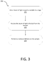
- FIG. 3 illustrates an embodiment of a method 200 .
- the method 200 includes directing a beam of light toward a sample on a stage at 201 .
- the sample is an aWLP wafer or a BE wafer.
- the beam of light reflected from the sample is received at a detector at 202 .
- a review of defects on the sample is performed at 203 using information from the detector.
- the method 200 includes at least one of: supplying a fluid between the sample and an optical objective by an immersion subsystem that includes a fluid supply unit; forming an illumination pattern for differential phase contrast with the beam of light; or the beam of light being at ultraviolet or deep ultraviolet wavelengths.
- the beam of light is generated by a plurality of LEDs.
- the LEDs may be colored.
- the beam of light reflected by the sample is imaged through at least one of the objectives to the detector using a relay lens.
- the beam of light from the relay lens can be converted into an image using a frame grabber module of the detector.
- the frame grabber module can be synchronized with the stage.
- the light source is the white light source.
- the light source further includes a color filter and a spatial filter.
- the method 200 includes generating, using the processor, an intensity image and a phase image.
- the intensity image and the phase image are generated as a function of height.
- the method 200 can further include generating, using the processor, a composite image from the intensity image and the phase image.
- the method 200 includes supplying the fluid, the beam of light forms the illumination pattern for the differential phase contrast, and the beam of light is at the ultraviolet or deep ultraviolet wavelengths.
- the embodiments described herein can be used for review and/or classification of defects on samples in an aWLP or BE.
- Immersion technology to review and classify defects, DPC technology to review and classify defects, focus scan with DPC technology to review and classify defects, polarization control to an illumination source and tube-lens with a quantitative modeling algorithm for DPC, or use one or more of these techniques with UV or DUV to review and classify defects can improve review and/or classification of defects on samples in a aWLP or BE.
Landscapes
- Physics & Mathematics (AREA)
- Chemical & Material Sciences (AREA)
- General Physics & Mathematics (AREA)
- Analytical Chemistry (AREA)
- Engineering & Computer Science (AREA)
- Optics & Photonics (AREA)
- Multimedia (AREA)
- General Health & Medical Sciences (AREA)
- Health & Medical Sciences (AREA)
- Life Sciences & Earth Sciences (AREA)
- Biochemistry (AREA)
- Immunology (AREA)
- Pathology (AREA)
- Computer Vision & Pattern Recognition (AREA)
- Oil, Petroleum & Natural Gas (AREA)
- Quality & Reliability (AREA)
- Theoretical Computer Science (AREA)
- Investigating Materials By The Use Of Optical Means Adapted For Particular Applications (AREA)
- Testing Or Measuring Of Semiconductors Or The Like (AREA)
Abstract
Description
Claims (14)
Priority Applications (6)
| Application Number | Priority Date | Filing Date | Title |
|---|---|---|---|
| US16/826,193 US11544838B2 (en) | 2020-03-21 | 2020-03-21 | Systems and methods of high-resolution review for semiconductor inspection in backend and wafer level packaging |
| PCT/US2020/027881 WO2021194515A1 (en) | 2020-03-21 | 2020-04-13 | Systems and methods of high-resolution review for semiconductor inspection in backend and wafer level packaging |
| EP20927161.8A EP4121747B1 (en) | 2020-03-21 | 2020-04-13 | Systems and methods of high-resolution review for semiconductor inspection in backend and wafer level packaging |
| KR1020227036679A KR102889865B1 (en) | 2020-03-21 | 2020-04-13 | High-resolution review system and method for semiconductor inspection in back-end and wafer-level packaging |
| CN202080098036.1A CN115244389B (en) | 2020-03-21 | 2020-04-13 | System and method for high resolution inspection of semiconductor inspection in back-end and wafer level packaging |
| TW110100730A TWI878427B (en) | 2020-03-21 | 2021-01-08 | Systems and methods of high-resolution review for semiconductor inspection in backend and wafer level packaging |
Applications Claiming Priority (1)
| Application Number | Priority Date | Filing Date | Title |
|---|---|---|---|
| US16/826,193 US11544838B2 (en) | 2020-03-21 | 2020-03-21 | Systems and methods of high-resolution review for semiconductor inspection in backend and wafer level packaging |
Publications (2)
| Publication Number | Publication Date |
|---|---|
| US20210295495A1 US20210295495A1 (en) | 2021-09-23 |
| US11544838B2 true US11544838B2 (en) | 2023-01-03 |
Family
ID=77748289
Family Applications (1)
| Application Number | Title | Priority Date | Filing Date |
|---|---|---|---|
| US16/826,193 Active 2040-09-19 US11544838B2 (en) | 2020-03-21 | 2020-03-21 | Systems and methods of high-resolution review for semiconductor inspection in backend and wafer level packaging |
Country Status (6)
| Country | Link |
|---|---|
| US (1) | US11544838B2 (en) |
| EP (1) | EP4121747B1 (en) |
| KR (1) | KR102889865B1 (en) |
| CN (1) | CN115244389B (en) |
| TW (1) | TWI878427B (en) |
| WO (1) | WO2021194515A1 (en) |
Families Citing this family (2)
| Publication number | Priority date | Publication date | Assignee | Title |
|---|---|---|---|---|
| KR20230048655A (en) * | 2021-10-05 | 2023-04-12 | 삼성전자주식회사 | Method of inspecting a wafer and apparatus for performing the same |
| CN119317938A (en) * | 2022-06-21 | 2025-01-14 | 株式会社日立高新技术 | Unsuitable detection device and unsuitable detection method |
Citations (22)
| Publication number | Priority date | Publication date | Assignee | Title |
|---|---|---|---|---|
| US6222936B1 (en) | 1998-02-03 | 2001-04-24 | Advanced Micro Devices, Inc. | Apparatus and method for reducing defects in a semiconductor lithographic process |
| US20020122174A1 (en) * | 2001-03-01 | 2002-09-05 | Akira Hamamatsu | .Apparatus and method for inspecting defects |
| US6495818B1 (en) * | 1998-07-21 | 2002-12-17 | The Institute For Technology Development | Microscopic hyperspectral imaging scanner |
| US6566671B1 (en) | 1999-06-17 | 2003-05-20 | Hitachi, Ltd. | Microscopic defect inspection apparatus and method thereof, as well as positional shift calculation circuit therefor |
| US20040262529A1 (en) * | 2003-01-29 | 2004-12-30 | Minoru Yoshida | Pattern defect inspection method and its apparatus |
| US20050264802A1 (en) | 2004-05-31 | 2005-12-01 | Yukihiro Shibata | Method and apparatus for inspecting defects and a system for inspecting defects |
| US7050223B1 (en) | 1999-07-09 | 2006-05-23 | Leica Microsystems Semiconductor Gmbh | DUV-capable microscope objective with parfocal IR focus |
| US7130037B1 (en) | 2003-01-09 | 2006-10-31 | Kla-Tencor Technologies Corp. | Systems for inspecting wafers and reticles with increased resolution |
| US20070280526A1 (en) | 2006-05-30 | 2007-12-06 | Irfan Malik | Determining Information about Defects or Binning Defects Detected on a Wafer after an Immersion Lithography Process is Performed on the Wafer |
| US7436527B2 (en) | 2004-03-04 | 2008-10-14 | Kla-Tencor Corporation | Systems and methods for immersion metrology |
| WO2009149103A1 (en) | 2008-06-03 | 2009-12-10 | Jeong Hwan J | Interferometric defect detection and classification |
| US20100219327A1 (en) | 2009-03-01 | 2010-09-02 | Arbore Mark A | High speed quantum efficiency measurement apparatus utilizing solid state lightsource |
| US20110141272A1 (en) * | 2008-09-30 | 2011-06-16 | Sachio Uto | Apparatus and method for inspecting an object surface defect |
| US20110164806A1 (en) * | 2007-08-22 | 2011-07-07 | Camtek Ltd. | Method and system for low cost inspection |
| US20120268738A1 (en) * | 2011-04-21 | 2012-10-25 | Jeffrey Drue David | Construction of Reference Spectra with Variations in Environmental Effects |
| US8488102B2 (en) | 2004-03-18 | 2013-07-16 | Taiwan Semiconductor Manufacturing Company, Ltd. | Immersion fluid for immersion lithography, and method of performing immersion lithography |
| US20130228684A1 (en) | 2005-08-12 | 2013-09-05 | Ebara Corporation | Detector and inspecting apparatus |
| US9809898B2 (en) | 2013-06-26 | 2017-11-07 | Lam Research Corporation | Electroplating and post-electrofill systems with integrated process edge imaging and metrology systems |
| US20180284032A1 (en) * | 2017-04-03 | 2018-10-04 | Samsung Electronics Co., Ltd. | Method of testing an object and apparatus for performing the same |
| US20180374738A1 (en) * | 2017-06-23 | 2018-12-27 | Samsung Electronics Co., Ltd. | Chip mounting apparatus and method using the same |
| US20190318948A1 (en) * | 2018-04-12 | 2019-10-17 | Taiwan Semiconductor Manufacturing Co., Ltd. | Wafer-level inspection using on-valve inspection detectors |
| US10563973B2 (en) * | 2016-03-28 | 2020-02-18 | Kla-Tencor Corporation | All surface film metrology system |
Family Cites Families (15)
| Publication number | Priority date | Publication date | Assignee | Title |
|---|---|---|---|---|
| JP3956942B2 (en) * | 1998-09-18 | 2007-08-08 | 株式会社日立製作所 | Defect inspection method and apparatus |
| JP2003149169A (en) * | 2001-11-16 | 2003-05-21 | Tokyo Seimitsu Co Ltd | Wafer defect examining device |
| WO2004072629A1 (en) * | 2003-02-17 | 2004-08-26 | Nanyang Technological University | System and method for inspection of silicon wafers |
| JP2005083800A (en) * | 2003-09-05 | 2005-03-31 | Hitachi Ltd | Defect inspection method and defect inspection apparatus |
| JP4875936B2 (en) * | 2006-07-07 | 2012-02-15 | 株式会社日立ハイテクノロジーズ | Foreign object / defect detection method and foreign object / defect inspection device |
| JP2009156687A (en) * | 2007-12-26 | 2009-07-16 | Hoya Corp | Defect inspection device of photomask, defect inspection method of photomask, and manufacturing method of photomask |
| JP5301293B2 (en) * | 2009-01-08 | 2013-09-25 | 株式会社日立ハイテクノロジーズ | Defect inspection apparatus and method |
| JP4716148B1 (en) * | 2010-03-30 | 2011-07-06 | レーザーテック株式会社 | Inspection apparatus, defect classification method, and defect detection method |
| US9864184B2 (en) * | 2012-10-30 | 2018-01-09 | California Institute Of Technology | Embedded pupil function recovery for fourier ptychographic imaging devices |
| WO2014164929A1 (en) * | 2013-03-11 | 2014-10-09 | Kla-Tencor Corporation | Defect detection using surface enhanced electric field |
| JP2014238534A (en) * | 2013-06-10 | 2014-12-18 | シャープ株式会社 | Inspection apparatus for light control film and manufacturing apparatus for light control film |
| CN110082900B (en) | 2013-08-22 | 2022-05-13 | 加州理工学院 | Variable Illumination Fourier Overlay Correlation Imaging Apparatus, System, and Method |
| SG11201607864SA (en) * | 2014-05-19 | 2016-10-28 | Univ California | Fourier ptychographic microscopy with multiplexed illumination |
| CN107111118B (en) | 2014-12-22 | 2019-12-10 | 加州理工学院 | EPI illumination Fourier ptychographic imaging for thick samples |
| JP6904414B2 (en) * | 2017-03-31 | 2021-07-14 | 株式会社ニコン | Liquid supply device, objective lens holding device, microscope, and liquid supply method |
-
2020
- 2020-03-21 US US16/826,193 patent/US11544838B2/en active Active
- 2020-04-13 KR KR1020227036679A patent/KR102889865B1/en active Active
- 2020-04-13 EP EP20927161.8A patent/EP4121747B1/en active Active
- 2020-04-13 WO PCT/US2020/027881 patent/WO2021194515A1/en not_active Ceased
- 2020-04-13 CN CN202080098036.1A patent/CN115244389B/en active Active
-
2021
- 2021-01-08 TW TW110100730A patent/TWI878427B/en active
Patent Citations (22)
| Publication number | Priority date | Publication date | Assignee | Title |
|---|---|---|---|---|
| US6222936B1 (en) | 1998-02-03 | 2001-04-24 | Advanced Micro Devices, Inc. | Apparatus and method for reducing defects in a semiconductor lithographic process |
| US6495818B1 (en) * | 1998-07-21 | 2002-12-17 | The Institute For Technology Development | Microscopic hyperspectral imaging scanner |
| US6566671B1 (en) | 1999-06-17 | 2003-05-20 | Hitachi, Ltd. | Microscopic defect inspection apparatus and method thereof, as well as positional shift calculation circuit therefor |
| US7050223B1 (en) | 1999-07-09 | 2006-05-23 | Leica Microsystems Semiconductor Gmbh | DUV-capable microscope objective with parfocal IR focus |
| US20020122174A1 (en) * | 2001-03-01 | 2002-09-05 | Akira Hamamatsu | .Apparatus and method for inspecting defects |
| US7130037B1 (en) | 2003-01-09 | 2006-10-31 | Kla-Tencor Technologies Corp. | Systems for inspecting wafers and reticles with increased resolution |
| US20040262529A1 (en) * | 2003-01-29 | 2004-12-30 | Minoru Yoshida | Pattern defect inspection method and its apparatus |
| US7436527B2 (en) | 2004-03-04 | 2008-10-14 | Kla-Tencor Corporation | Systems and methods for immersion metrology |
| US8488102B2 (en) | 2004-03-18 | 2013-07-16 | Taiwan Semiconductor Manufacturing Company, Ltd. | Immersion fluid for immersion lithography, and method of performing immersion lithography |
| US20050264802A1 (en) | 2004-05-31 | 2005-12-01 | Yukihiro Shibata | Method and apparatus for inspecting defects and a system for inspecting defects |
| US20130228684A1 (en) | 2005-08-12 | 2013-09-05 | Ebara Corporation | Detector and inspecting apparatus |
| US20070280526A1 (en) | 2006-05-30 | 2007-12-06 | Irfan Malik | Determining Information about Defects or Binning Defects Detected on a Wafer after an Immersion Lithography Process is Performed on the Wafer |
| US20110164806A1 (en) * | 2007-08-22 | 2011-07-07 | Camtek Ltd. | Method and system for low cost inspection |
| WO2009149103A1 (en) | 2008-06-03 | 2009-12-10 | Jeong Hwan J | Interferometric defect detection and classification |
| US20110141272A1 (en) * | 2008-09-30 | 2011-06-16 | Sachio Uto | Apparatus and method for inspecting an object surface defect |
| US20100219327A1 (en) | 2009-03-01 | 2010-09-02 | Arbore Mark A | High speed quantum efficiency measurement apparatus utilizing solid state lightsource |
| US20120268738A1 (en) * | 2011-04-21 | 2012-10-25 | Jeffrey Drue David | Construction of Reference Spectra with Variations in Environmental Effects |
| US9809898B2 (en) | 2013-06-26 | 2017-11-07 | Lam Research Corporation | Electroplating and post-electrofill systems with integrated process edge imaging and metrology systems |
| US10563973B2 (en) * | 2016-03-28 | 2020-02-18 | Kla-Tencor Corporation | All surface film metrology system |
| US20180284032A1 (en) * | 2017-04-03 | 2018-10-04 | Samsung Electronics Co., Ltd. | Method of testing an object and apparatus for performing the same |
| US20180374738A1 (en) * | 2017-06-23 | 2018-12-27 | Samsung Electronics Co., Ltd. | Chip mounting apparatus and method using the same |
| US20190318948A1 (en) * | 2018-04-12 | 2019-10-17 | Taiwan Semiconductor Manufacturing Co., Ltd. | Wafer-level inspection using on-valve inspection detectors |
Non-Patent Citations (7)
| Title |
|---|
| Chen et al., 3D Differential Phase Contrast Microscopy, Biomedial Optics Express, vol. 7, No. 10, 3940-3950, 2016. |
| Chen et al., 3D Differential Phase Contrast Microscopy, Quantitative Phase Imaging II, Proc. of SPIE, vol. 9718, 971826, 2016. |
| Hillmann et al., DUV Water Immersion Technology Extends Linearity First Results from the New 65nm Node CD Metrology System LWM500 WI, 21st Euro. Mask and Lithography Conf., Proc. of SPIE, vol. 5835, 2005. |
| KLA-Tencor, "KLA-Tencor Introduces Wafer Inspection and Review Systems," Silicon Semiconductor, Jul. 12, 2016. |
| Tian & Waller, Quantitative Differential Phase Contrast Imaging in an LED Array Microscope, Optics Express, vol. 23, No. 9, 11394, 2015. |
| Vollrath, Ultra-High-Resolution DUV Microscope Optics for Semiconductor Applications, Proc. of SPIE 58650E, 2005. |
| WIPO, ISR for PCT/US2020/027881, dated Dec. 4, 2020. |
Also Published As
| Publication number | Publication date |
|---|---|
| US20210295495A1 (en) | 2021-09-23 |
| CN115244389A (en) | 2022-10-25 |
| EP4121747A1 (en) | 2023-01-25 |
| KR102889865B1 (en) | 2025-11-21 |
| EP4121747B1 (en) | 2026-02-18 |
| TW202136754A (en) | 2021-10-01 |
| KR20220156076A (en) | 2022-11-24 |
| EP4121747A4 (en) | 2024-04-17 |
| TWI878427B (en) | 2025-04-01 |
| CN115244389B (en) | 2025-08-19 |
| WO2021194515A1 (en) | 2021-09-30 |
Similar Documents
| Publication | Publication Date | Title |
|---|---|---|
| US10801953B2 (en) | Semiconductor metrology based on hyperspectral imaging | |
| US12288318B2 (en) | Ultra-micro defect detection apparatus and detection method thereof | |
| JP5487196B2 (en) | A split field inspection system using a small catadioptric objective. | |
| TWI721993B (en) | Methods and apparatus for measuring height on a semiconductor wafer | |
| US9305341B2 (en) | System and method for measurement of through silicon structures | |
| US20140132948A1 (en) | Apparatus and Method for Optical Metrology with Optimized System Parameters | |
| KR20210107149A (en) | Methods and systems for inspection of semiconductor structures with automatically generated defect features | |
| CN110609039A (en) | An optical detection device and method thereof | |
| KR20190049890A (en) | Defect marking for semiconductor wafer inspection | |
| CN109690238B (en) | Speed Enhancement for Chroma Confocal Metrology | |
| CN106772923B (en) | Automatic focusing method and system based on inclined slit | |
| TW201409021A (en) | Inspection system for inspecting the surface defects of the specimen and the method thereof | |
| KR20220031687A (en) | Methods and systems for optical surface defect material characterization | |
| US7746459B2 (en) | Systems configured to inspect a wafer | |
| US20250076216A1 (en) | Method and apparatus for detecting defects in a package | |
| US11544838B2 (en) | Systems and methods of high-resolution review for semiconductor inspection in backend and wafer level packaging | |
| KR20260057330A (en) | Method and apparatus for detecting defects within a package | |
| WO2025048721A1 (en) | System and method for die inspections |
Legal Events
| Date | Code | Title | Description |
|---|---|---|---|
| FEPP | Fee payment procedure |
Free format text: ENTITY STATUS SET TO UNDISCOUNTED (ORIGINAL EVENT CODE: BIG.); ENTITY STATUS OF PATENT OWNER: LARGE ENTITY |
|
| AS | Assignment |
Owner name: KLA CORPORATION, CALIFORNIA Free format text: ASSIGNMENT OF ASSIGNORS INTEREST;ASSIGNOR:LI, SHIFANG;REEL/FRAME:052923/0989 Effective date: 20200526 |
|
| STPP | Information on status: patent application and granting procedure in general |
Free format text: DOCKETED NEW CASE - READY FOR EXAMINATION |
|
| STPP | Information on status: patent application and granting procedure in general |
Free format text: NON FINAL ACTION MAILED |
|
| STPP | Information on status: patent application and granting procedure in general |
Free format text: RESPONSE TO NON-FINAL OFFICE ACTION ENTERED AND FORWARDED TO EXAMINER |
|
| STPP | Information on status: patent application and granting procedure in general |
Free format text: FINAL REJECTION MAILED |
|
| STPP | Information on status: patent application and granting procedure in general |
Free format text: RESPONSE AFTER FINAL ACTION FORWARDED TO EXAMINER |
|
| STPP | Information on status: patent application and granting procedure in general |
Free format text: ADVISORY ACTION MAILED |
|
| STPP | Information on status: patent application and granting procedure in general |
Free format text: NOTICE OF ALLOWANCE MAILED -- APPLICATION RECEIVED IN OFFICE OF PUBLICATIONS |
|
| STPP | Information on status: patent application and granting procedure in general |
Free format text: PUBLICATIONS -- ISSUE FEE PAYMENT VERIFIED |
|
| STCF | Information on status: patent grant |
Free format text: PATENTED CASE |