US11539012B2 - Organic light-emitting device - Google Patents
Organic light-emitting device Download PDFInfo
- Publication number
- US11539012B2 US11539012B2 US16/944,248 US202016944248A US11539012B2 US 11539012 B2 US11539012 B2 US 11539012B2 US 202016944248 A US202016944248 A US 202016944248A US 11539012 B2 US11539012 B2 US 11539012B2
- Authority
- US
- United States
- Prior art keywords
- group
- substituted
- sensitizer
- unsubstituted
- organic light
- Prior art date
- Legal status (The legal status is an assumption and is not a legal conclusion. Google has not performed a legal analysis and makes no representation as to the accuracy of the status listed.)
- Active, expires
Links
Images


Classifications
-
- H—ELECTRICITY
- H10—SEMICONDUCTOR DEVICES; ELECTRIC SOLID-STATE DEVICES NOT OTHERWISE PROVIDED FOR
- H10K—ORGANIC ELECTRIC SOLID-STATE DEVICES
- H10K85/00—Organic materials used in the body or electrodes of devices covered by this subclass
- H10K85/30—Coordination compounds
- H10K85/341—Transition metal complexes, e.g. Ru(II)polypyridine complexes
- H10K85/346—Transition metal complexes, e.g. Ru(II)polypyridine complexes comprising platinum
-
- H01L51/5004—
-
- H01L51/0087—
-
- H01L51/5016—
-
- H01L51/5024—
-
- H01L51/5056—
-
- H01L51/5072—
-
- H—ELECTRICITY
- H10—SEMICONDUCTOR DEVICES; ELECTRIC SOLID-STATE DEVICES NOT OTHERWISE PROVIDED FOR
- H10K—ORGANIC ELECTRIC SOLID-STATE DEVICES
- H10K50/00—Organic light-emitting devices
- H10K50/10—OLEDs or polymer light-emitting diodes [PLED]
- H10K50/11—OLEDs or polymer light-emitting diodes [PLED] characterised by the electroluminescent [EL] layers
- H10K50/12—OLEDs or polymer light-emitting diodes [PLED] characterised by the electroluminescent [EL] layers comprising dopants
- H10K50/121—OLEDs or polymer light-emitting diodes [PLED] characterised by the electroluminescent [EL] layers comprising dopants for assisting energy transfer, e.g. sensitization
-
- H—ELECTRICITY
- H10—SEMICONDUCTOR DEVICES; ELECTRIC SOLID-STATE DEVICES NOT OTHERWISE PROVIDED FOR
- H10K—ORGANIC ELECTRIC SOLID-STATE DEVICES
- H10K50/00—Organic light-emitting devices
- H10K50/10—OLEDs or polymer light-emitting diodes [PLED]
- H10K50/14—Carrier transporting layers
- H10K50/15—Hole transporting layers
-
- H—ELECTRICITY
- H10—SEMICONDUCTOR DEVICES; ELECTRIC SOLID-STATE DEVICES NOT OTHERWISE PROVIDED FOR
- H10K—ORGANIC ELECTRIC SOLID-STATE DEVICES
- H10K50/00—Organic light-emitting devices
- H10K50/10—OLEDs or polymer light-emitting diodes [PLED]
- H10K50/14—Carrier transporting layers
- H10K50/16—Electron transporting layers
-
- H—ELECTRICITY
- H10—SEMICONDUCTOR DEVICES; ELECTRIC SOLID-STATE DEVICES NOT OTHERWISE PROVIDED FOR
- H10K—ORGANIC ELECTRIC SOLID-STATE DEVICES
- H10K85/00—Organic materials used in the body or electrodes of devices covered by this subclass
- H10K85/40—Organosilicon compounds, e.g. TIPS pentacene
-
- H—ELECTRICITY
- H10—SEMICONDUCTOR DEVICES; ELECTRIC SOLID-STATE DEVICES NOT OTHERWISE PROVIDED FOR
- H10K—ORGANIC ELECTRIC SOLID-STATE DEVICES
- H10K85/00—Organic materials used in the body or electrodes of devices covered by this subclass
- H10K85/60—Organic compounds having low molecular weight
- H10K85/649—Aromatic compounds comprising a hetero atom
- H10K85/657—Polycyclic condensed heteroaromatic hydrocarbons
- H10K85/6572—Polycyclic condensed heteroaromatic hydrocarbons comprising only nitrogen in the heteroaromatic polycondensed ring system, e.g. phenanthroline or carbazole
-
- H—ELECTRICITY
- H10—SEMICONDUCTOR DEVICES; ELECTRIC SOLID-STATE DEVICES NOT OTHERWISE PROVIDED FOR
- H10K—ORGANIC ELECTRIC SOLID-STATE DEVICES
- H10K2101/00—Properties of the organic materials covered by group H10K85/00
- H10K2101/10—Triplet emission
-
- H—ELECTRICITY
- H10—SEMICONDUCTOR DEVICES; ELECTRIC SOLID-STATE DEVICES NOT OTHERWISE PROVIDED FOR
- H10K—ORGANIC ELECTRIC SOLID-STATE DEVICES
- H10K2101/00—Properties of the organic materials covered by group H10K85/00
- H10K2101/30—Highest occupied molecular orbital [HOMO], lowest unoccupied molecular orbital [LUMO] or Fermi energy values
-
- H—ELECTRICITY
- H10—SEMICONDUCTOR DEVICES; ELECTRIC SOLID-STATE DEVICES NOT OTHERWISE PROVIDED FOR
- H10K—ORGANIC ELECTRIC SOLID-STATE DEVICES
- H10K2101/00—Properties of the organic materials covered by group H10K85/00
- H10K2101/40—Interrelation of parameters between multiple constituent active layers or sublayers, e.g. HOMO values in adjacent layers
-
- H—ELECTRICITY
- H10—SEMICONDUCTOR DEVICES; ELECTRIC SOLID-STATE DEVICES NOT OTHERWISE PROVIDED FOR
- H10K—ORGANIC ELECTRIC SOLID-STATE DEVICES
- H10K2101/00—Properties of the organic materials covered by group H10K85/00
- H10K2101/90—Multiple hosts in the emissive layer
-
- H—ELECTRICITY
- H10—SEMICONDUCTOR DEVICES; ELECTRIC SOLID-STATE DEVICES NOT OTHERWISE PROVIDED FOR
- H10K—ORGANIC ELECTRIC SOLID-STATE DEVICES
- H10K59/00—Integrated devices, or assemblies of multiple devices, comprising at least one organic light-emitting element covered by group H10K50/00
- H10K59/30—Devices specially adapted for multicolour light emission
- H10K59/32—Stacked devices having two or more layers, each emitting at different wavelengths
Definitions
- One or more embodiments provide an organic light-emitting device including a host, a dopant, and a sensitizer.
- Organic light-emitting devices are self-emission devices that produce full-color images, and also have wide viewing angles, high contrast ratios, short response times, and excellent characteristics in terms of brightness, driving voltage, and response speed, compared to devices in the art.
- an organic light-emitting device includes an anode, a cathode, and an organic layer between the anode and the cathode, wherein the organic layer includes an emission layer.
- a hole transport region may be between the anode and the emission layer, and an electron transport region may be between the emission layer and the cathode.
- Holes provided from the anode may move toward the emission layer through the hole transport region, and electrons provided from the cathode may move toward the emission layer through the electron transport region.
- the holes and the electrons recombine in the emission layer to produce excitons. These excitons transit from an excited state to a ground state, thereby generating light.
- One or more embodiments provide an organic light-emitting device including a certain host, a certain dopant, and a certain sensitizer.
- an organic light-emitting device including a first electrode, a second electrode, and an organic layer between the first electrode and the second electrode,
- the organic layer includes an emission layer
- the emission layer includes a host, a dopant, and a sensitizer
- the sensitizer includes ruthenium (Ru), palladium (Pd), rhenium (Re), osmium (Os), or platinum (Pt), and
- ⁇ E ST (S) is a difference between a lowest excitation singlet energy level and a lowest excitation triplet energy level of the sensitizer
- HOMO(D) is a highest occupied molecular orbital (HOMO) energy level of the dopant
- HOMO(S) is a HOMO energy level of the sensitizer.
- an organic light-emitting device including a first electrode, a second electrode, m emission units located between the first electrode and the second electrode and including at least one emission layer,
- m ⁇ 1 charge generating layers located between two adjacent emission units among the m emission units and including an n-type charge generating layer and a p-type charge generating layer
- n is an integer of 2 or more
- a maximum emission wavelength of light emitted from at least one emission unit among the m emission units is different from a maximum emission wavelength of light emitted from at least one emission unit among the remaining emission units
- the emission layer includes a host, a dopant, and a sensitizer, and
- the dopant and the sensitizer satisfy the Conditions 1 and 2 described above.
- an organic light-emitting device including a first electrode, a second electrode, and m emission layers between the first electrode and the second electrode,
- n is an integer of 2 or more
- a maximum emission wavelength of light emitted from at least one emission layer among the m emission layers is different from a maximum emission wavelength of light emitted from at least one emission layer among the remaining emission layers
- the emission layer includes a host, a dopant, and a sensitizer, and
- the dopant and the sensitizer satisfy Conditions 1 and 2 described above.
- FIG. 1 shows a schematic cross-sectional view of an organic light-emitting device according to an exemplary embodiment
- FIG. 2 shows a diagram schematically illustrating energy transfer in an emission layer of an organic light-emitting device according to an exemplary embodiment
- FIG. 3 is a schematic cross-sectional view of an organic light-emitting device according to another exemplary embodiment.
- FIG. 4 is a schematic cross-sectional view of an organic light-emitting device according to another exemplary embodiment.
- relative terms such as “lower” or “bottom” and “upper” or “top,” may be used herein to describe one element's relationship to another element as illustrated in the Figures It will be understood that relative terms are intended to encompass different orientations of the device in addition to the orientation depicted in the Figures
- the exemplary term “lower,” can therefore, encompasses both an orientation of “lower” and “upper,” depending on the particular orientation of the figure
- elements described as “below” or “beneath” other elements would then be oriented “above” the other elements
- the exemplary terms “below” or “beneath” can, therefore, encompass both an orientation of above and below.
- “About” or “approximately” as used herein is inclusive of the stated value and means within an acceptable range of deviation for the particular value as determined by one of ordinary skill in the art, considering the measurement in question and the error associated with measurement of the particular quantity (i.e., the limitations of the measurement system). For example, “about” can mean within one or more standard deviations, or within ⁇ 30%, 20%, 10% or 5% of the stated value.
- Exemplary embodiments are described herein with reference to cross section illustrations that are schematic illustrations of idealized embodiments As such, variations from the shapes of the illustrations as a result, for example, of manufacturing techniques and/or tolerances, are to be expected Thus, embodiments described herein should not be construed as limited to the particular shapes of regions as illustrated herein but are to include deviations in shapes that result, for example, from manufacturing. For example, a region illustrated or described as flat may, typically, have rough and/or nonlinear features Moreover, sharp angles that are illustrated may be rounded Thus, the regions illustrated in the figures are schematic in nature and their shapes are not intended to illustrate the precise shape of a region and are not intended to limit the scope of the present claims.
- FIG. 1 is a schematic view of an organic light-emitting device 10 according to an exemplary embodiment.
- a structure and a manufacturing method of an organic light-emitting device according to an example of the present disclosure will be described with reference to FIG. 1 .
- the organic light-emitting device 10 of FIG. 1 includes a first electrode 11 , a second electrode 19 facing the first electrode 11 , and an organic layer 10 A between the first electrode 11 and the second electrode 19 .
- the organic layer 10 A includes an emission layer 15 , a hole transport region 12 is located between the first electrode 11 and the emission layer 15 , and an electron transport region 17 is located between the emission layer 15 and the second electrode 19 .
- a substrate may be additionally located under the first electrode 11 or above the second electrode 19 .
- the substrate any substrate that is used in organic light-emitting devices available in the art may be used, and the substrate may be a glass substrate or a transparent plastic substrate, each having excellent mechanical strength, thermal stability, transparency, surface smoothness, ease of handling, and water resistance.
- the first electrode 11 may be formed by depositing or sputtering a material for forming the first electrode 11 on the substrate.
- the first electrode 11 may be an anode.
- the material for forming the first electrode 11 may be a material with a high work function to facilitate hole injection.
- the first electrode 11 may be a reflective electrode, a semi-transmissive electrode, or a transmissive electrode.
- a material for forming a first electrode may be indium tin oxide (ITO), indium zinc oxide (IZO), tin oxide (SnO 2 ), zinc oxide (ZnO), or any combinations thereof, but embodiments of the present disclosure are not limited thereto.
- a material for forming a first electrode may be magnesium (Mg), silver (Ag), aluminum (Al), aluminum-lithium (Al—Li), calcium (Ca), magnesium-indium (Mg—In), magnesium-silver (Mg—Ag), or any combinations thereof, but embodiments of the present disclosure are not limited thereto.
- the first electrode 11 may have a single-layered structure or a multi-layered structure including two or more layers.
- the emission layer 15 includes a host, a dopant, and a sensitizer.
- the emission layer 15 emits fluorescent light. That is, the dopant is a material that may emit fluorescent light. The emission layer 15 emitting the fluorescent light is clearly distinguished from an emission layer emitting phosphorescent light.
- the emission layer 15 may include a host, a dopant, and a sensitizer,
- ⁇ E ST (S) is a difference between a lowest excitation singlet energy level and a lowest excitation triplet energy level of the sensitizer
- HOMO(D) is a highest occupied molecular orbital (HOMO) energy level of the dopant
- HOMO(S) is a HOMO energy level of the sensitizer.
- Each of the lowest excitation singlet energy level and the lowest excitation triplet energy level of the sensitizer is evaluated by using a DFT method of a Gaussian 09 program which is structurally optimized at B3LYP/6-31G(d,p) level.
- Each of the HOMO energy levels of the dopant and the sensitizer is a value calculated from a reduction onset potential measured by using cyclic voltammetry (CV).
- stability of the sensitizer in particular, stability at the lowest excitation triplet energy level, may be ensured. Accordingly, stability of an organic light-emitting device including the sensitizer may be improved, and roll-off characteristics may be improved.
- the lifespan of an organic light-emitting device may be improved.
- the dopant may have a relatively high hole trap characteristic.
- the hole trap characteristic of the dopant may be improved, thereby allowing holes to be well transmitted from the dopant to the sensitizer. Accordingly, an organic light-emitting device may be controlled not to emit light in a certain region in an emission layer, and thus the deterioration of the dopant due to high exciton energy is suppressed.
- the organic light-emitting device may have improved lifespan characteristics.
- the organic light-emitting device may further satisfy Condition 1-1 below: 0.2 eV ⁇ E ST ( S ) ⁇ 0.4 eV. ⁇ Condition 1-1>
- ⁇ E ST (S) is a difference between a lowest excitation singlet energy level and a lowest excitation triplet energy level of the sensitizer.
- the sensitizer necessarily includes an atom such as Pt, and thus the full width at half maximum of the sensitizer may be relatively small. Accordingly, color reproducibility of the organic light-emitting device may be improved.
- the sensitizer may satisfy Condition 3 below: T 1 ( S ) ⁇ 2.63 eV. ⁇ Condition 3>
- T 1 (S) is the lowest triplet excitation energy level of the sensitizer.
- the sensitizer may further satisfy Condition 4 below: HOMO( S ) ⁇ 6.0 eV. ⁇ Condition 4>
- HOMO(S) is a HOMO energy level of the sensitizer.
- 75% of triplet excitons formed in the host are transmitted to a sensitizer via Dexter energy transfer, and the energy of 25% of singlet excitons formed in the host are transferred to a singlet and triplet of the sensitizer.
- the energy transferred to the singlet intersystem crosses to the triplet, and then the triplet energy of the sensitizer is transferred to a dopant via Forster energy transfer.
- both singlet excitons and triplet excitons, generated in an emission layer, are transmitted to a dopant, and thus an organic light-emitting device with improved efficiency may be obtained.
- the organic light-emitting device since an organic light-emitting device in which energy loss is significantly reduced may be obtained, the organic light-emitting device may have improved lifespan characteristics.
- An amount of the sensitizer in the emission layer may be selected within the range of 5 wt % to 50 wt %. When the amount of the sensitizer is within this range, efficient energy transfer in an emission layer may be achieved, and an organic light-emitting device with high efficiency and long lifespan may be implemented.
- the host, the dopant, and the sensitizer may further satisfy Condition 6 below: T 1 ( H ) ⁇ T 1 ( S ) ⁇ S 1 ( D ). ⁇ Condition 6>
- T 1 (H) is a lowest excitation triplet energy level of the host
- S 1 (D) is a lowest excitation singlet energy level of the dopant
- T 1 (S) is a lowest excitation triplet energy level of the sensitizer.
- triplet excitons in an emission layer may be efficiently transmitted to the dopant, and thus an organic light-emitting device with improved efficiency may be obtained.
- the emission layer may consist of the host, the dopant, and the sensitizer. That is, the emission layer may not further include materials other than the host, the dopant, and the sensitizer.
- a thickness of the emission layer may be in a range of about 100 ⁇ to about 1,000 ⁇ , for example, about 200 ⁇ to about 600 ⁇ . When the thickness of the emission layer is within the range, excellent light-emission characteristics may be obtained without a substantial increase in driving voltage.
- a proportion of emission components emitted from the dopant may be 90% or more.
- the host may include no metal atoms.
- the host may include one kind of host.
- the one host may be an amphoteric host, an electron transport host, and a hole transport host, which will be described later.
- the host may include a mixture of two or more different hosts.
- the host may be a mixture of an electron transport host and a hole transport host, a mixture of two types of electron transport hosts different from each other, or a mixture of two types of hole transport hosts different from each other.
- the electron transport host and the hole transport host may be understood by referring to the related description to be disclosed herein.
- the host may include an electron transport host including at least one electron transport moiety, a hole transport host that is free of an electron transport moiety, or any combination thereof.
- the electron transport moiety used herein may be a cyano group, a ⁇ electron-deficient nitrogen-containing C 1 -C 60 cyclic group, or a group represented by one of the following formulae:
- *, *′, and *′′ are each a binding site to a neighboring atom.
- the electron transport host of the emission layer 15 may include at least one of a cyano group, a ⁇ electron-deficient nitrogen-containing C 1 -C 60 cyclic group, or any combination thereof.
- the electron transport host in the emission layer 15 may include at least one cyano group.
- the electron transport host in the emission layer 15 may include at least one cyano group, at least one ⁇ electron deficient nitrogen-containing C 1 -C 60 cyclic group, or any combination thereof.
- the host may include an electron transport host and a hole transport host, wherein the electron transport host may include at least one ⁇ electron-rich C 3 -C 60 cyclic group, at least one electron transport moiety, or any combination thereof, and the hole transport host may include at least one ⁇ electron-rich C 3 -C 60 cyclic group and may not include an electron transport moiety.
- ⁇ electron-deficient nitrogen-containing C 1 -C 60 cyclic group refers to a cyclic group having at least one *—N ⁇ *′ moiety, and for example, may be an imidazole group, a pyrazole group, a thiazole group, an isothiazole group, an oxazole group, an isoxazole group, a pyridine group, a pyrazine group, a pyridazine group, a pyrimidine group, an indazole group, a purine group, a quinoline group, an isoquinoline group, a benzoquinoline group, a phthalazine group, a naphthyridine group, a quinoxaline group, a quinazoline group, a cinnoline group, a phenanthridine group, an acridine group, a phenanthroline group, a phenazine group, a benz
- the ⁇ electron-rich C 3 -C 60 cyclic group may be a benzene group, a heptalene group, an indene group, a naphthalene group, an azulene group, an indacene group, acenaphthylene group, a fluorene group, a spiro-bifluorene group, a benzofluorene group, a dibenzofluorene group, a phenalene group, a phenanthrene group, an anthracene group, a fluoranthene group, a triphenylene group, a pyrene group, a chrysene group, a naphthacene group, a picene group, a perylene group, a pentacene group, a hexacene group, a pentacene group, a rubicene group, a corogen group, an ovalene group,
- the electron transport host may be a compound represented by Formula E-1, and
- the hole transport host may be compounds represented by Formula H-1, but embodiments of the present disclosure are not limited thereto: [Ar 301 ] xb11 -[(L 301 ) xb1 -R 301 ] xb21 . ⁇ Formula E-1>
- Ar 301 may be a substituted or unsubstituted C 5 -C 60 carbocyclic group and a substituted or unsubstituted C 1 -C 60 heterocyclic group,
- xb11 may be 1, 2, or 3,
- L 301 may each independently be a single bond, a group represented by the following formula, a substituted or unsubstituted C 5 -C 60 carbocyclic group, or a substituted or unsubstituted C 1 -C 60 heterocyclic group, and * and in the following formulae are each a binding site to a neighboring atom,
- xb1 may be an integer from 1 to 5
- R 301 may be hydrogen, deuterium, —F, —Cl, —Br, —I, a hydroxyl group, a cyano group, a nitro group, an amidino group, a hydrazine group, a hydrazone group, a substituted or unsubstituted C 1 -C 60 alkyl group, a substituted or unsubstituted C 2 -C 60 alkenyl group, a substituted or unsubstituted C 2 -C 60 alkynyl group, a substituted or unsubstituted C 1 -C 60 alkoxy group, a substituted or unsubstituted C 1 -C 60 alkylthio group, a substituted or unsubstituted C 3 -C 10 cycloalkyl group, a substituted or unsubstituted C 1 -C 10 heterocycloalkyl group, a substituted or unsubstituted C 3 -C 10
- xb21 may be an integer from 1 to 5
- Q 301 to Q 303 may each independently be a C 1 -C 10 alkyl group, a C 1 -C 10 alkoxy group, a phenyl group, a biphenyl group, a terphenyl group, or a naphthyl group, and
- Ar 301 , L 301 , and R 301 in Formula E-1 may each independently include a ⁇ electron-deficient nitrogen-containing C 1 -C 60 cyclic group;
- L 301 in Formula E-1 is a group represented by the following formulae:
- R 301 in Formula E-1 may be a cyano group, —S( ⁇ O) 2 (Q 301 ), —S( ⁇ O)(Q 301 ), —P( ⁇ O)(Q 301 )(Q 302 ), or —P( ⁇ S)(Q 301 )(Q 302 ).
- Ar 401 -(L 401 ) xd1 -(Ar 402 ) xd11 ⁇ Formula H-1>
- L 401 may be:
- xd1 may be an integer from 1 to 10, wherein when xd1 is 2 or more, two or more of L 401 (s) may be identical to or different from each other,
- Ar 401 may be a group represented by Formulae 11 or 12,
- Ar 402 may be:
- a group represented by Formula 11 or 12 a phenyl group, a naphthyl group, a fluorenyl group, a carbazolyl group, a dibenzofuranyl group, a dibenzothiophenyl group, a biphenyl group, a terphenyl group, or a triphenylenyl group; or
- CY 401 and CY 402 may each independently be a benzene group, a naphthalene group, a fluorene group, a carbazole group, a benzocarbazole group, an indolocarbazole group, a dibenzofuran group, a dibenzothiophene group, a dibenzosilole group, a benzonaphthofuran group, a benzonaphthothiophene group, or a benzonaphthosilole group,
- a 21 may be a single bond, O, S, N(R 51 ), C(R 51 )(R 52 ), or Si(R 51 )(R 52 ),
- a 22 may be a single bond, O, S, N(R 53 ), C(R 53 )(R 54 ), or Si(R 53 )(R 54 ),
- At least one A 21 , A 22 , or any combination thereof in Formula 12 is not a single bond
- R 51 to R 54 , R 60 , and R 70 may each independently be:
- a ⁇ electron-rich C 3 -C 60 cyclic group for example, a phenyl group, a naphthyl group, a fluorenyl group, a carbazolyl group, a dibenzofuranyl group, a dibenzothiophenyl group, a biphenyl group, a terphenyl group, or a triphenylenyl group;
- a ⁇ electron-rich C 3 -C 60 cyclic group for example, a phenyl group, a naphthyl group, a fluorenyl group, a carbazolyl group, a dibenzofuranyl group, a dibenzothiophenyl group, a biphenyl group, a terphenyl group, or a triphenylenyl group, each substituted with at least one deuterium, a hydroxyl group, an amino group, an amidino group, a hydrazine group, a hydrazone group, a carboxylic acid or a salt thereof, a sulfonic acid or a salt thereof, a phosphoric acid or a salt thereof, a C 1 -C 20 alkyl group, a C 1 -C 20 alkoxy group, a phenyl group, a naphthyl group, a fluorenyl group, a carbazolyl group, a dibenzofur
- e1 and e2 are each independently an integer from 0 to 10,
- Q 401 to Q 406 may each independently be hydrogen, deuterium, a hydroxyl group, an amino group, an amidino group, a hydrazine group, a hydrazone group, a carboxylic acid or a salt thereof, a sulfonic acid or a salt thereof, a phosphoric acid or a salt thereof, a phenyl group, a naphthyl group, a fluorenyl group, a carbazolyl group, a dibenzofuranyl group, a dibenzothiophenyl group, a biphenyl group, a terphenyl group, or a triphenylenyl group, and
- * indicates a binding site to a neighboring atom.
- Ar 301 and L 301 in Formula E-1 may each independently be a benzene group, a naphthalene group, a fluorene group, a spiro-bifluorene group, a benzofluorene group, a dibenzofluorene group, a phenalene group, a phenanthrene group, an anthracene group, a fluoranthene group, a triphenylene group, a pyrene group, a chrysene group, a naphthacene group, a picene group, a perylene group, a pentaphene group, an indenoanthracene group, a dibenzofuran group, a dibenzothiophene group, an imidazole group, a pyrazole group, a thiazole group, an isothiazole group, an oxazole group, an isoxazole group,
- L 301 (s) in the number of xb1 may each independently be an imidazole group, a pyrazole group, a thiazole group, an isothiazole group, an oxazole group, an isoxazole group, a pyridine group, a pyrazine group, a pyridazine group, a pyrimidine group, an indazole group, a purine group, a quinoline group, an isoquinoline group, a benzoquinoline group, a phthalazine group, a naphthyridine group, a quinoxaline group, a quinazoline group, a cinnoline group, a phenanthridine group, an acridine group, a phenanthroline group, a phenazine group, a benzimidazole group, an isobenzothiazole group, a benzoxazole group, an isobenzoxazole group
- R 301 may be hydrogen, deuterium, —F, —Cl, —Br, —I, a hydroxyl group, a cyano group, a nitro group, an amidino group, a hydrazine group, a hydrazone group, a C 1 -C 20 alkyl group, a C 1 -C 20 alkoxy group, a phenyl group, a biphenyl group, a terphenyl group, a tetraphenyl group, a naphthyl group, a cyano group-containing phenyl group, a cyano group-containing biphenyl group, a cyano group-containing terphenyl group, a cyano group-containing tetraphenyl group, a cyano group-containing naphthyl group, a pyridinyl group, a phenylpyridinyl group, a diphenylpyridinyl group,
- Q 31 to Q 33 may each independently be a C 1 -C 10 alkyl group, a C 1 -C 10 alkoxy group, a phenyl group, a biphenyl group, a terphenyl group, and a naphthyl group, but embodiments of the present disclosure are not limited thereto.
- Ar 301 may be a benzene group, a naphthalene group, a fluorene group, a spiro-bifluorene group, a benzofluorene group, a dibenzofluorene group, a phenalene group, a phenanthrene group, an anthracene group, a fluoranthene group, a triphenylene group, a pyrene group, a chrysene group, a naphthacene group, a picene group, a perylene group, a pentaphene group, an indenoanthracene group, a dibenzofuran group, or a dibenzothiophene group, each unsubstituted or substituted with at least one deuterium, —F, —CI, —Br, —I, a hydroxyl group, a cyano group, a nitro group, an amidino group,
- L 301 may be groups represented by Formulae 5-1 to 5-3 and Formulae 6-1 to 6-33:
- Z 1 may be hydrogen, deuterium, —F, —Cl, —Br, —I, a hydroxyl group, a cyano group, a nitro group, an amidino group, a hydrazine group, a hydrazone group, a C 1 -C 20 alkyl group, a C 1 -C 20 alkoxy group, a phenyl group, a biphenyl group, a terphenyl group, a naphthyl group, a cyano group-containing phenyl group, a cyano group-containing biphenyl group, a cyano group-containing terphenyl group, a cyano group-containing naphthyl group, a pyridinyl group, a phenylpyridinyl group, a diphenylpyridinyl group, a biphenylpyridinyl group, a di(biphenyl)pyridinyl group
- d4 may be 0, 1, 2, 3, or 4,
- d3 may be 0, 1, 2, or 3,
- d2 may be 0, 1, or 2
- * and *′ each indicate a binding site to a neighboring atom.
- L 301 may be groups represented by Formulae 5-2, 5-3, and 6-8 to 6-33.
- R 301 may be a cyano group or a group represented by one of Formulae 7-1 to 7-18, and at least one of Ar 402 (s) in the number of xd11 may be a group represented by one of Formulae 7-1 to 7-18, but embodiments of the present disclosure are not limited thereto:
- xb41 to xb44 may each be 0, 1, or 2, wherein xb41 in Formula 7-10 is not 0, the sum of xb41 and xb42 in Formulae 7-11 to 7-13 is not 0, the sum of xb41, xb42, and xb43 in Formulae 7-14 to 7-16 is not 0, the sum of xb41, xb42, xb43, and xb44 in Formulae 7-17 and 7-18 is not 0, and * indicates a binding site to a neighboring atom.
- Two or more Ar 301 (s) in Formula E-1 may be identical to or different from each other, two or more L 301 (s) may be identical to or different from each other, two or more L 401 (s) in Formula H-1 may be identical to or different from each other, and two or more Ar 402 (s) in Formula H-1 may be identical to or different from each other.
- the electron transport host includes i) at least one of a cyano group, a pyrimidine group, a pyrazine group, a triazine group, or any combination thereof, and ii) a triphenylene group, and the hole transport host may include a carbazole group.
- the electron transport host may include at least one cyano group.
- the electron transport host may be, for example, of Groups HE1 to HE7, but embodiments of the present disclosure are not limited thereto:
- the hole transport host may be one of Compounds H-H1 to H-H106, but embodiments of the present disclosure are not limited thereto:
- amphoteric host may be Group HEH1, but embodiments of the present disclosure are not limited thereto:
- Ph may be a phenyl group.
- the weight ratio of the electron transport host to the hole transport host may be 1:9 to 9:1, for example, 2:8 to 8:2, for example, 4:6 to 6:4, for example, 5:5.
- the hole-and-electron transport balance in the emission layer 15 may be made.
- organic light-emitting devices Since the dopant emits fluorescent light, organic light-emitting devices according to an embodiment of the present disclosure are clearly distinguished from organic light-emitting devices containing compounds that emit phosphorescent light.
- a maximum emission wavelength of an emission spectrum of the dopant may be 400 nm or more and 550 nm or less.
- the maximum emission wavelength of the emission spectrum of the dopant may be 400 nm or more and 495 nm or less, or 450 nm or more and 495 nm or less, but embodiments of the present disclosure are not limited thereto.
- the dopant may emit blue light.
- the “maximum emission wavelength” refers to a wavelength at which the emission intensity is the greatest, and may also be referred to as “a peak emission wavelength”.
- the dopant may be free of metal atoms.
- the dopant may be a condensed polycyclic compound or a styryl-based compound.
- the dopant may include one of a naphthalene-containing core, a fluorene-containing core, a spiro-bifluorene-containing core, a benzofluorene-containing core, a dibenzofluorene-containing core, a phenanthrene-containing core, an anthracene-containing core, a fluoranthene-containing core, a triphenylene-containing core, a pyrene-containing core, a chrysene-containing core, a naphthacene-containing core, a picene-containing core, a perylene-containing core, a pentaphene-containing core, an indenoanthracene-containing core, a tetracene-containing core, a bisanthracene-containing core, or a core represented by one of Formulae 501-1 to 501-18, but embodiments of the present disclosure are not limited thereto:
- the dopant may be a styryl-amine-based compound or a styryl-carbazole-based compound, but embodiments of the present disclosure are not limited thereto.
- the dopant may be a compound represented by one of Formula 501:
- Ar 501 may be:
- a naphthalene group a fluorene group, a spiro-bifluorene group, a benzofluorene group, a dibenzofluorene group, a phenanthrene group, an anthracene group, a fluoranthene group, a triphenylene group, a pyrene group, a chrysene group, a naphthacene group, a picene group, a perylene group, a pentaphene group, an indenoanthracene group, a tetracene group, a bisanthracene group, or a group represented by one of Formulae 501-1 to 501-18; or
- a naphthalene group a fluorene group, a spiro-bifluorene group, a benzofluorene group, a dibenzofluorene group, a phenanthrene group, an anthracene group, a fluoranthene group, a triphenylene group, a pyrene group, a chrysene group, a naphthacene group, a picene group, a perylene group, a pentaphene indenoanthracene group, a tetracene group, a bisanthracene group, or a group represented by Formulae 501-1 to 501-18, each substituted with at least one deuterium, —F, —Cl, —Br, —I, a hydroxyl group, a cyano group, a nitro group, an amino group, an amidino group, a hydrazine group, a hydr
- L 501 to L 503 may each independently be a substituted or unsubstituted C 3 -C 10 cycloalkylene group, a substituted or unsubstituted C 1 -C 10 heterocycloalkylene group, a substituted or unsubstituted C 3 -C 10 cycloalkenylene group, a substituted or unsubstituted C 1 -C 10 heterocycloalkenylene group, a substituted or unsubstituted C 6 -C 60 arylene group, a substituted or unsubstituted C 1 -C 60 heteroarylene group, a substituted or unsubstituted divalent non-aromatic condensed polycyclic group, or a substituted or unsubstituted divalent non-aromatic condensed heteropolycyclic group,
- R 501 to R 508 may each independently be:
- a phenyl group a biphenyl group, a terphenyl group, a naphthyl group, a fluorenyl group, a spiro-bifluorenyl group, a benzofluorenyl group, a dibenzofluorenyl group, a phenanthrenyl group, an anthracenyl group, a pyrenyl group, a chrysenyl group, a pyridinyl group, a pyrazinyl group, a pyrimidinyl group, a pyridazinyl group, a quinolinyl group, an isoquinolinyl group, a quinoxalinyl group, a quinazolinyl group, a carbazole group, a triazinyl group, a dibenzofuranyl group, or a dibenzothiophenyl group; or
- a phenyl group a biphenyl group, a terphenyl group, a naphthyl group, a fluorenyl group, a spiro-bifluorenyl group, a benzofluorenyl group, a dibenzofluorenyl group, a phenanthrenyl group, an anthracenyl group, a pyrenyl group, a chrysenyl group, a pyridinyl group, a pyrazinyl group, a pyrimidinyl group, a pyridazinyl group, a quinolinyl group, an isoquinolinyl group, a quinoxalinyl group, a quinazolinyl group, a carbazolyl group, a triazinyl group, a dibenzofuranyl group, or a dibenzothiophenyl group, each substituted with at least one deuterium,
- xd1 to xd3 may each independently be 0, 1, 2, or 3, and
- xd4 may be 0, 1, 2, 3, 4, 5, or 6.
- Ar 501 may be:
- a naphthalene group a fluorene group, a spiro-bifluorene group, a benzofluorene group, a dibenzofluorene group, a phenanthrene group, an anthracene group, a fluoranthene group, a triphenylene group, a pyrene group, a chrysene group, a naphthacene group, a picene group, a perylene group, a pentaphene group, an indenoanthracene group, a tetracene group, a bisanthracene group, or a group represented by one of Formulae 501-1 to 501-18; or
- a naphthalene group a fluorene group, a spiro-bifluorene group, a benzofluorene group, a dibenzofluorene group, a phenanthrene group, an anthracene group, a fluoranthene group, a triphenylene group, a pyrene group, a chrysene group, a naphthacene group, a picene group, a perylene group, a pentaphene group, an indenoanthracene group, a tetracene group, a bisanthracene group, or a group represented by one of Formula 501-1 to 501-18, each substituted with at least one deuterium, —F, —Cl, —Br, —I, a hydroxyl group, a cyano group, a nitro group, an amino group, an amidino group, a hydrazine group,
- L 501 to L 503 are the same as described in connection with L 21 ,
- xd1 to xd3 may each independently be 0, 1, or 2, and
- xd4 may be 0, 1, 2, or 3, but embodiments of the present disclosure are not limited thereto.
- the dopant may include a compound represented by one of Formulae 502-1 to 502-5:
- X 51 may be N or C-[(L 501 ) xd1 -R 501 ], X 52 may be N or C-[(L 502 ) xd2 -R 502 ], X 53 may be N or C-[(L 503 ) xd3 -R 503 ], X 54 may be N or C-[(L 504 ) xd4 -R 504 ], X 55 may be N or C-[(L 505 ) xd5 -R 505 ], X 56 may be N or C-[(L 506 ) xd6 -R 506 ], X 57 may be N or C-[(L 507 ) xd7 -R 507 ], and X 58 may be N or C-[(L 508 ) xd8 -R 508 ],
- L 501 to L 508 are each the same as described in connection with L 501 in Formula 501,
- xd1 to xd8 are each the same as described in connection with xd1 in Formula 501,
- R 501 to R 508 may each independently be:
- a phenyl group a biphenyl group, a terphenyl group, a naphthyl group, a fluorenyl group, a spiro-bifluorenyl group, a benzofluorenyl group, a dibenzofluorenyl group, a phenanthrenyl group, an anthracenyl group, a pyrenyl group, a chrysenyl group, a pyridinyl group, a pyrazinyl group, a pyrimidinyl group, a pyridazinyl group, a quinolinyl group, an isoquinolinyl group, a quinoxalinyl group, a quinazolinyl group, a carbazole group, a triazinyl group, a dibenzofuranyl group, or a dibenzothiophenyl group; or
- a phenyl group a biphenyl group, a terphenyl group, a naphthyl group, a fluorenyl group, a spiro-bifluorenyl group, a benzofluorenyl group, a dibenzofluorenyl group, a phenanthrenyl group, an anthracenyl group, a pyrenyl group, a chrysenyl group, a pyridinyl group, a pyrazinyl group, a pyrimidinyl group, a pyridazinyl group, a quinolinyl group, an isoquinolinyl group, a quinoxalinyl group, a quinazolinyl group, a carbazolyl group, a triazinyl group, a dibenzofuranyl group, or a dibenzothiophenyl group, each substituted with at least one deuterium,
- xd11 and xd12 may each independently be an integer from 0 to 5
- R 501 to R 504 may optionally be linked together to form a saturated or unsaturated ring
- R 505 to R 508 may optionally be linked together to form a saturated or unsaturated ring.
- the dopant may include a compound represented by Formula 503:
- X 501 may be N, B, P( ⁇ )(R 504 ), or P( ⁇ S)(R 504 ),
- Y 501 to Y 502 may each independently be O, S, N(R 505 ), B(R 505 ), C(R 505 )(R 506 ), or Si(R 505 )(R 506 ),
- k501 may be 0 or 1, wherein, when k501 is 0, —(Y 501 ) k501 — may not exist,
- a 501 to A 503 may each independently be a C 5 -C 30 carbocyclic group or a C 1 -C 30 heterocyclic group,
- L 501 to L 503 are the same as described in connection with L 501 in Formula 501,
- xd1 to xd are the same as described in connection with xd1 in Formula 501,
- R 501 to R 506 may each independently be hydrogen, deuterium, —F, —Cl, —Br, —I, a hydroxyl group, a cyano group, a nitro group, an amino group, an amidino group, a hydrazine group, a hydrazone group, a carboxylic acid group or a salt thereof, a sulfonic acid group or a salt thereof, a phosphoric acid group or a salt thereof, a substituted or unsubstituted C 1 -C 60 alkyl group, a substituted or unsubstituted C 2 -C 60 alkenyl group, a substituted or unsubstituted C 2 -C 60 alkynyl group, a substituted or unsubstituted C 1 -C 60 alkoxy group, a substituted or unsubstituted C 1 -C 60 alkylthio group, a substituted or unsubstituted C 3 -C
- xd11 and xd12 may each independently be an integer from 0 to 5, and
- Q 1 to Q 3 , Q 21 to Q 23 , and Q 31 to Q 33 may each be independently hydrogen, deuterium, —F, —Cl, —Br, —I, a hydroxyl group, a cyano group, a nitro group, an amidino group, a hydrazino group, a hydrazono group, a C 1 -C 60 alkyl group, a C 2 -C 60 alkenyl group, a C 2 -C 60 alkynyl group, a C 1 -C 60 alkoxy group, a C 1 -C 60 alkylthio group, a C 3 -C 10 cycloalkyl group, a C 1 -C 10 heterocycloalkyl group, a C 3 -C 10 cycloalkenyl group, a C 1 -C 10 heterocycloalkenyl group, a C 6 -C 60 aryl group, a C 6 -C 60 aryloxy group
- the dopant may include at least one compound, for example, of the following Compounds FD(1) to FD(16) and FD1 to FD24:
- the amount of the dopant in the emission layer may be about 0.01 wt % to about 15 wt %, but embodiments of the present disclosure are not limited thereto.
- the sensitizer may include ruthenium (Ru), palladium (Pd), rhenium (Re), osmium (Os), or platinum (Pt).
- the sensitizer may be a phosphorescent dopant compound.
- the sensitizer may include a metal (M 11 ) ruthenium (Ru), palladium (Pd), rhenium (Re), osmium (Os), or platinum (Pt), and an organic ligand (L 11 ), and L 11 and M 11 may form 1, 2, 3, or 4 cyclometallated ring(s).
- the sensitizer may include an organometallic compound represented by Formula 101: M 11 (L 11 ) n11 (L 12 ) n12 . ⁇ Formula 101>
- M 11 is ruthenium (Ru), palladium (Pd), rhenium (Re), osmium (Os), or platinum (Pt),
- L 11 is a ligand represented by one of Formulae 1-1 to 1-4,
- L 12 may be a monodentate ligand or a bidentate ligand
- n11 may be 1,
- n12 may be 0, 1, or 2
- a 1 to A 4 may each independently be a substituted or unsubstituted C 5 -C 30 carbocyclic group, a substituted or unsubstituted C 1 -C 30 heterocyclic group, or a non-cyclic group,
- Y 11 to Y 14 may each independently be a chemical bond, O, S, N(R 91 ), B(R 91 ), P(R 91 ), or C(R 91 )(R 92 ),
- T 1 to T 4 may each independently be a single bond, a double bond, *—N(R 93 )—*′, *—B(R 93 )—*′, *—P(R 93 )—*′, *—C(R 93 )(R 94 )—*′, *—Si(R 93 )(R 94 )—*′, *—Ge(R 93 )(R 94 )—*′, *—S—*′, *—Se—*′, *—O—*′, *—C( ⁇ O)—*, *—S( ⁇ O)—*′, *—S( ⁇ O) 2 —*′, *—C(R 93 ) ⁇ *′, * ⁇ C(R 93 )—*′, *—C(R 93 ) ⁇ C(R 94 )—*′, *—C( ⁇ S)—*′, or *—C ⁇ C—*′,
- a substituent of the substituted C 5 -C 30 carbocyclic group, a substituent of the substituted C 1 -C 30 heterocyclic group, and R 91 to R 94 may each independently be hydrogen, deuterium, —F, —Cl, —Br, —I, —SF 5 , a hydroxyl group, a cyano group, a nitro group, an amidino group, a hydrazine group, a hydrazone group, a carboxylic acid or a salt thereof, a sulfonic acid or a salt thereof, a phosphoric acid or a salt thereof, a substituted or unsubstituted C 1 -C 60 alkyl group, a substituted or unsubstituted C 2 -C 60 alkenyl group, a substituted or unsubstituted C 2 -C 60 alkynyl group, a substituted or unsubstituted C 1 -C 60 alkoxy group,
- * 1 , * 2 , * 3 , and * 4 each indicate a binding site to M 11 .
- Q 1 to Q 3 may each independently be hydrogen, deuterium, —F, —Cl, —Br, —I, a hydroxyl group, a cyano group, a nitro group, an amidino group, a hydrazine group, a hydrazone group, a C 1 -C 60 alkyl group, a C 2 -C 60 alkenyl group, a C 2 -C 60 alkynyl group, a C 1 -C 60 alkoxy group, a substituted or unsubstituted C 1 -C 60 alkylthio group, a C 3 -C 10 cycloalkyl group, a C 1 -C 10 heterocycloalkyl group, a C 3 -C 10 cycloalkenyl group, a C 1 -C 10 heterocycloalkenyl group, a C 6 -C 60 aryl group, a C 7 -C 60 alkyl aryl group, a C 6
- the sensitizer may be Groups I to VI, but embodiments of the present disclosure are not limited thereto:
- the hole transport region 12 may be located between the first electrode 11 and the emission layer 15 of the organic light-emitting device 10 .
- the hole transport region 12 may have a single-layered structure or a multi-layered structure.
- the hole transport region 12 may have a hole injection layer, a hole transport layer, a hole injection layer/hole transport layer structure, a hole injection layer/first hole transport layer/second hole transport layer structure, a hole transport layer/middle layer structure, a hole injection layer/hole transport layer/middle layer structure, a hole transport layer/electron blocking layer, or hole injection layer/hole transport layer/electron blocking layer structure, but embodiments of the present disclosure are not limited thereto.
- the hole transport region 12 may include any compound having hole transport properties.
- the hole transport region 12 may include an amine-based compound.
- the hole transport region 12 may include at least one of a compound represented by Formula 201 to a compound represented by Formula 205, but embodiments of the present disclosure are not limited thereto:
- L 201 to L 209 may each independently be *—O—*′, *—S—*′, a substituted or unsubstituted C 5 -C 60 carbocyclic group, or a substituted or unsubstituted C 1 -C 60 heterocyclic group,
- xa1 to xa9 may each independently be an integer from 0 to 5, and
- R 201 to R 206 may each independently be a substituted or unsubstituted C 3 -C 10 cycloalkyl group, a substituted or unsubstituted C 1 -C 10 heterocycloalkyl group, a substituted or unsubstituted C 3 -C 10 cycloalkenyl group, a substituted or unsubstituted C 1 -C 10 heterocycloalkenyl group, a substituted or unsubstituted C 6 -C 60 aryl group, a substituted or unsubstituted C 6 -C 60 aryloxy group, a substituted or unsubstituted C 6 -C 60 arylthio group, a substituted or unsubstituted C 1 -C 60 heteroaryl group, a substituted or unsubstituted monovalent non-aromatic condensed polycyclic group, or a substituted or unsubstituted monovalent non-aromatic condensed heteropol
- L 201 to L 209 may be a benzene group, a heptalene group, an indene group, a naphthalene group, an azulene group, a heptalene group, an indacene group, an acenaphthylene group, a fluorene group, a spiro-bifluorene group, a benzofluorene group, a dibenzofluorene group, a phenalene group, a phenanthrene group, an anthracene group, a fluoranthene group, a triphenylene group, a pyrene group, a chrysene group, a naphthacene group, a picene group, a perylene group, a pentacene group, a hexacene group, a pentacene group, a rubicene group, a corogen group, an ovalene
- xa1 to xa9 may each independently be 0, 1, or 2, and
- R 201 to R 206 may each independently be a phenyl group, a biphenyl group, a terphenyl group, a pentalenyl group, an indenyl group, a naphthyl group, an azulenyl group, a heptalenyl group, an indacenyl group, an acenaphthyl group, a fluorenyl group, a spiro-bifluorenyl group, a benzofluorenyl group, a dibenzofluorenyl group, a phenalenyl group, a phenanthrenyl group, an anthracenyl group, a fluoranthenyl group, a triphenylenyl group, a pyrenyl group, a chrysenyl group, a naphthacenyl group, a picenyl group, a perylenyl group, a penta
- Q 11 to Q 13 and Q 31 to Q 33 may each independently be a C 1 -C 10 alkyl group, a C 1 -C 10 alkoxy group, a phenyl group, a biphenyl group, a terphenyl group, or a naphthyl group.
- the hole transport region 12 may include a carbazole-containing amine-based compound.
- the hole transport region 12 may include a carbazole-containing amine-based compound or a carbazole-free amine-based compound.
- the carbazole-containing amine-based compound may be, for example, of compounds represented by Formula 201 including a carbazole group and further including at least one of a dibenzofuran group, a dibenzothiophene group, a fluorene group, a spiro-bifluorene group, an indenocarbazole group, an indolocarbazole group, a benzofurocarbazole group, a benzothienocarbazole group, or any combination thereof.
- Formula 201 including a carbazole group and further including at least one of a dibenzofuran group, a dibenzothiophene group, a fluorene group, a spiro-bifluorene group, an indenocarbazole group, an indolocarbazole group, a benzofurocarbazole group, a benzothienocarbazole group, or any combination thereof.
- the carbazole-free amine-based compound may be, for example, of compounds represented by Formula 201 which do not include a carbazole group and which include at least one a dibenzofuran group, a dibenzothiophene group, a fluorene group, a spiro-bifluorene group, an indenocarbazole group, an indolocarbazole group, a benzofurocarbazole group, a benzothienocarbazole group, or any combination thereof.
- Formula 201 which do not include a carbazole group and which include at least one a dibenzofuran group, a dibenzothiophene group, a fluorene group, a spiro-bifluorene group, an indenocarbazole group, an indolocarbazole group, a benzofurocarbazole group, a benzothienocarbazole group, or any combination thereof.
- the hole transport region 12 may include at least one compound represented by Formulae 201, 202, or any combination thereof.
- the hole transport region 12 may include at least one of the compounds represented by Formulae 201-1, 202-1, 201-2, or any combination thereof, but embodiments of the present disclosure are not limited thereto:
- L 201 to L 203 , L 205 , xa1 to xa3, xa5, R 201 , and R 202 are the same as described herein, and R 211 to R 213 are each independently hydrogen, deuterium, —F, —Cl, —Br, —I, a hydroxyl group, a cyano group, a nitro group, an amidino group, a hydrazine group, a hydrazone group, a C 1 -C 20 alkyl group, a C 1 -C 20 alkoxy group, a phenyl group, a biphenyl group, a terphenyl group, a phenyl group substituted with a C 1 -C 10 alkyl group, or a phenyl group substituted with —F, a naphthyl group, a fluorenyl group, a spiro-bifluoren
- the hole transport region 12 may include at least one of Compounds HT1 to HT39, but embodiments of the present disclosure are not limited thereto.
- hole transport region 12 of the organic light-emitting device 10 may further include a p-dopant.
- the hole transport region 12 may have a matrix (for example, at least one of the compounds represented by Formulae 201 to 205) and a p-dopant included in the matrix.
- the p-dopant may be uniformly or non-uniformly doped in the hole transport region 12 .
- a lowest unoccupied molecular orbital (LUMO) energy level of the p-dopant may be ⁇ 3.5 eV or less.
- the p-dopant may include at least one of a quinone derivative, a metal oxide, a cyano group-containing compound, or any combination thereof, but embodiments of the present disclosure are not limited thereto.
- the p-dopant may include at least one of:
- a quinone derivative such as tetracyanoquinodimethane (TCNQ), 2,3,5,6-tetrafluoro-7,7,8,8-tetracyanoquinodimethane (F4-TCNQ), or F6-TCNNQ;
- a metal oxide such as tungsten oxide or molybdenum oxide
- R 221 to R 223 may each independently be a substituted or unsubstituted C 3 -C 10 cycloalkyl group, a substituted or unsubstituted C 1 -C 10 heterocycloalkyl group, a substituted or unsubstituted C 3 -C 10 cycloalkenyl group, a substituted or unsubstituted C 1 -C 10 heterocycloalkenyl group, a substituted or unsubstituted C 6 -C 60 aryl group, a substituted or unsubstituted C 1 -C 60 heteroaryl group, a substituted or unsubstituted monovalent non-aromatic condensed polycyclic group, and a substituted or unsubstituted monovalent non-aromatic condensed heteropolycyclic group, and at least one of R 221 to R 223 may have at least one of a cyano group, —F, —Cl, —Br, —I
- the hole transport region 12 may have a thickness of about 100 ⁇ to about 10,000 ⁇ , for example, about 400 ⁇ to about 2,000 ⁇ , and the emission layer 15 may have a thickness of about 100 ⁇ to about 3,000 ⁇ , for example, about 300 ⁇ to about 1,000 ⁇ .
- the thickness of each of the hole transport region 12 and the emission layer 15 is within these ranges described above, satisfactory hole transportation characteristics and/or luminescent characteristics may be obtained without a substantial increase in driving voltage.
- the electron transport region 17 is placed between the emission layer 15 and the second electrode 19 of the organic light-emitting device 10 .
- the electron transport region 17 may have a single-layered structure or a multi-layered structure.
- the electron transport region 17 may have an electron transport layer, an electron transport layer/electron injection layer structure, a buffer layer/electron transport layer structure, a hole blocking layer/electron transport layer structure, a buffer layer/electron transport layer/electron injection layer structure, or a hole blocking layer/electron transport layer/electron injection layer structure, but embodiments of the present disclosure are not limited thereto.
- the electron transport region 17 may further include an electron control layer.
- the electron transport region 17 may include known electron transport materials.
- the electron transport region 17 may include a metal-free compound containing at least one ⁇ electron-deficient nitrogen-containing C 1 -C 60 cyclic group.
- the ⁇ electron-deficient nitrogen-containing C 1 -C 60 cyclic group is the same as described above.
- the electron transport region 17 may include a compound represented by Formula 601: [Ar 601 ] xe11 -[(L 601 ) xe1 -R 601 ] xe21 .
- Formula 601 [Ar 601 ] xe11 -[(L 601 ) xe1 -R 601 ] xe21 .
- Ar 601 and L 601 may each independently be a substituted or unsubstituted C 5 -C 60 carbocyclic group or a substituted or unsubstituted C 1 -C 60 heterocyclic group,
- xe11 may be 1, 2, or 3,
- xe1 may be an integer from 0 to 5
- R 601 may be a substituted or unsubstituted C 3 -C 10 cycloalkyl group, a substituted or unsubstituted C 1 -C 10 heterocycloalkyl group, a substituted or unsubstituted C 3 -C 10 cycloalkenyl group, a substituted or unsubstituted C 1 -C 10 heterocycloalkenyl group, a substituted or unsubstituted C 6 -C 60 aryl group, a substituted or unsubstituted C 6 -C 60 aryloxy group, a substituted or unsubstituted C 6 -C 60 arylthio group, a substituted or unsubstituted C 1 -C 60 heteroaryl group, a substituted or unsubstituted monovalent non-aromatic condensed polycyclic group, a substituted or unsubstituted monovalent non-aromatic condensed heteropolycyclic group, —
- Q 601 to Q 603 may each independently be a C 1 -C 10 alkyl group, a C 1 -C 10 alkoxy group, a phenyl group, a biphenyl group, a terphenyl group, or a naphthyl group, and
- xe21 may be an integer from 1 to 5.
- At least one of Ar 601 (s) in the number of xe11 and R 601 (s) in the number of xe21 may include the ⁇ electron-deficient nitrogen-containing C 1 -C 60 cyclic group.
- ring Ar 601 and L 601 in Formula 601 may each independently be a benzene group, a naphthalene group, a fluorene group, a spiro-bifluorene group, a benzofluorene group, a dibenzofluorene group, a phenalene group, a phenanthrene group, an anthracene group, a fluoranthene group, a triphenylene group, a pyrene group, a chrysene group, a naphthacene group, a picene group, a perylene group, a pentaphene group, an indenoanthracene group, a dibenzofuran group, a dibenzothiophene group, a carbazole group, an imidazole group, a pyrazole group, a thiazole group, an isothiazole group, an oxazole group
- Q 31 to Q 33 may each independently be a C 1 -C 10 alkyl group, a C 1 -C 10 alkoxy group, a phenyl group, a biphenyl group, a terphenyl group, or a naphthyl group.
- xe11 in Formula 601 is 2 or more, two or more Ar 601 (s) may be linked to each other via a single bond.
- Ar 601 in Formula 601 may be an anthracene group.
- the compound represented by Formula 601 may be represented by Formula 601-1:
- X 614 may be N or C(R 614 ), X 615 may be N or C(R 615 ), X 616 may be N or C(R 616 ), at least one of X 614 to X 616 may be N,
- L 611 to L 613 may each independently be the same as described in connection with the L 601 ,
- xe611 to xe613 may each independently be the same as described in connection with xe1,
- R 611 to R 613 may each independently be the same as described in connection with R 601 , and
- R 614 to R 616 may each independently be hydrogen, deuterium, —F, —Cl, —Br, —I, a hydroxyl group, a cyano group, a nitro group, an amidino group, a hydrazino group, a hydrazono group, a C 1 -C 20 alkyl group, a C 1 -C 20 alkoxy group, a phenyl group, a biphenyl group, a terphenyl group, or a naphthyl group.
- xe1 and xe611 to xe613 in Formulae 601 and 601-1 may each independently be 0, 1, or 2.
- R 601 and R 611 to R 613 in Formulae 601 and 601-1 may each independently be: a phenyl group, a biphenyl group, a terphenyl group, a naphthyl group, a fluorenyl group, a spiro-bifluorenyl group, a benzofluorenyl group, a dibenzofluorenyl group, a phenanthrenyl group, an anthracenyl group, a fluoranthenyl group, a triphenylenyl group, a pyrenyl group, a chrysenyl group, a perylenyl group, a pentaphenyl group, a hexacenyl group, a pentacenyl group, a thiophenyl group, a furanyl group, a carbazolyl group, an indolyl group, an isoindolyl
- the electron transport region 17 may include at least one compound of Compounds ET1 to ET36, but embodiments of the present disclosure are not limited thereto:
- the electron transport region 17 may include at least one of 2,9-dimethyl-4,7-diphenyl-1,10-phenanthroline (BCP), 4,7-dphenyl-1,10-phenanthroline (Bphen), Alq 3 , BAlq, 3-(biphenyl-4-yl)-5-(4-tert-butylphenyl)-4-phenyl-4H-1,2,4-triazole (TAZ), NTAZ, or any combination thereof:
- Thicknesses of the buffer layer, the hole blocking layer, and the electron control layer may each independently be in a range of about 20 ⁇ to about 1,000 ⁇ , for example, about 30 ⁇ to about 300 ⁇ . When the thicknesses of the buffer layer, the hole blocking layer, and the electron control layer are within these ranges, excellent hole blocking characteristics or electron control characteristics may be obtained without a substantial increase in driving voltage.
- a thickness of the electron transport layer may be in a range of about 100 ⁇ to about 1,000 ⁇ , for example, about 150 ⁇ to about 500 ⁇ . When the thickness of the electron transport layer is within the range described above, the electron transport layer may have satisfactory electron transport characteristics without a substantial increase in driving voltage.
- the electron transport region 17 (for example, the electron transport layer in the electron transport region 17 ) may further include, in addition to the materials described above, a metal-containing material.
- the metal-containing material may include at least one of an alkali metal complex, an alkaline earth-metal complex, or any combination thereof.
- the alkali metal complex may include a metal ion such as a Li ion, a Na ion, a K ion, a Rb ion, or a Cs ion
- the alkaline earth-metal complex may include a metal ion such as a Be ion, a Mg ion, a Ca ion, a Sr ion, or a Ba ion.
- a ligand coordinated with the metal ion of the alkali metal complex or the alkaline earth-metal complex may be a hydroxy quinoline, a hydroxy isoquinoline, a hydroxy benzoquinoline, a hydroxy acridine, a hydroxy phenanthridine, a hydroxy phenyloxazole, a hydroxy phenylthiazole, a hydroxy diphenyloxadiazole, a hydroxy diphenylthiadiazole, a hydroxy phenylpyridine, a hydroxy phenylbenzimidazole, a hydroxy phenylbenzothiazole, a bipyridine, a phenanthroline, and a cyclopentadiene, but embodiments of the present disclosure are not limited thereto.
- the metal-containing material may include a Li complex.
- the Li complex may include, for example, Compound ET-D1 (lithium 8-hydroxyquinolate, LiQ) or ET-D2.
- the electron transport region 17 may include an electron injection layer that facilitates injection of electrons from the second electrode 19 .
- the electron injection layer may directly contact the second electrode 19 .
- the electron injection layer may have i) a single-layered structure including a single layer including a single material, ii) a single-layered structure including a single layer including a plurality of different materials, or iii) a multi-layered structure having a plurality of layers including a plurality of different materials.
- the electron injection layer may include an alkali metal, an alkaline earth metal, a rare earth metal, an alkali metal compound, an alkaline earth metal compound, a rare earth metal compound, an alkali metal complex, an alkaline earth-metal complex, a rare earth metal complex, or any combination thereof.
- the alkali metal may be Li, Na, K, Rb, or Cs. In one or more embodiments, the alkali metal may be Li, Na, or Cs. In one or more embodiments, the alkali metal may be Li or Cs, but embodiments of the present disclosure are not limited thereto.
- the alkaline earth metal may be Mg, Ca, Sr, or Ba.
- the rare earth metal may be Sc, Y, Ce, Tb, Yb, or Gd.
- the alkali metal compound, the alkaline earth-metal compound, or the rare earth metal compound may be an oxide or a halide (for example, fluorides, chlorides, bromides, or iodides) of the alkali metal, the alkaline earth-metal, or the rare earth metal.
- a halide for example, fluorides, chlorides, bromides, or iodides
- the alkali metal compound may be an alkali metal oxide, such as Li 2 O, Cs 2 O, or K 2 O, or an alkali metal halide, such as LiF, NaF, CsF, KF, LiI, NaI, CsI, or KI.
- the alkali metal compound may be LiF, Li 2 O, NaF, LiI, NaI, CsI, or KI, but embodiments of the present disclosure are not limited thereto.
- the alkaline earth metal compound may be BaO, SrO, CaO, Ba x Sr 1-x O (0 ⁇ x ⁇ 1), or Ba x Ca 1-x O (0 ⁇ x ⁇ 1). In one or more embodiments, the alkaline earth metal compound may be BaO, SrO, or CaO, but embodiments of the present disclosure are not limited thereto.
- the rare earth metal compound may be YbF 3 , ScF 3 , ScO 3 , Y 2 O 3 , Ce 2 O 3 , GdF 3 , or TbF 3 .
- the rare earth metal compound may be YbF 3 , ScF 3 , TbF 3 , YbI 3 , ScI 3 , or TbI 3 , but embodiments of the present disclosure are not limited thereto.
- the alkali metal complex, the alkaline earth-metal complex, and the rare earth metal complex may include an ion of alkali metal, alkaline earth-metal, or rare earth metal as described above, and a ligand coordinated with a metal ion of the alkali metal complex, the alkaline earth-metal complex, or the rare earth metal complex may be hydroxy quinoline, hydroxy isoquinoline, hydroxy benzoquinoline, hydroxy acridine, hydroxy phenanthridine, hydroxy phenyloxazole, hydroxy phenylthiazole, hydroxy diphenyloxadiazole, hydroxy diphenylthiadiazole, hydroxy phenylpyridine, hydroxy phenylbenzimidazole, hydroxy phenylbenzothiazole, bipyridine, phenanthroline, or cyclopentadiene, but embodiments of the present disclosure are not limited thereto.
- the electron injection layer may consist of an alkali metal, an alkaline earth metal, a rare earth metal, an alkali metal compound, an alkaline earth-metal compound, a rare earth metal compound, an alkali metal complex, an alkaline earth-metal complex, a rare earth metal complex, or any combinations thereof, as described above.
- the electron injection layer may further include an organic material.
- an alkali metal, an alkaline earth metal, a rare earth metal, an alkali metal compound, an alkaline earth-metal compound, a rare earth metal compound, an alkali metal complex, an alkaline earth-metal complex, a rare earth metal complex, or any combinations thereof may be homogeneously or non-homogeneously dispersed in a matrix including the organic material.
- a thickness of the electron injection layer may be in a range of about 1 ⁇ to about 100 ⁇ , for example, about 3 ⁇ to about 90 ⁇ . When the thickness of the electron injection layer is within the range described above, the electron injection layer may have satisfactory electron injection characteristics without a substantial increase in driving voltage.
- the second electrode 19 is located on the organic layer 10 A having such a structure.
- the second electrode 19 may be a cathode which is an electron injection electrode, and in this regard, a material for forming the second electrode 19 may be a metal, an alloy, an electrically conductive compound, and a combination thereof, which have a relatively low work function.
- the second electrode 19 may include at least one lithium (Li), silver (Ag), magnesium (Mg), aluminum (Al), aluminum-lithium (Al—Li), calcium (Ca), magnesium-indium (Mg—In), magnesium-silver (Mg—Ag), ITO, IZO, or any combination thereof, but embodiments of the present disclosure are not limited thereto.
- the second electrode 19 may be a transmissive electrode, a semi-transmissive electrode, or a reflective electrode.
- the second electrode 19 may have a single-layered structure having a single layer or a multi-layered structure including two or more layers.
- the organic light-emitting device 10 has been described with reference to FIG. 1 , but embodiments of the present disclosure are not limited thereto.
- FIG. 3 is a schematic cross-sectional view of an organic light-emitting device 100 according to another exemplary embodiment.
- the organic light-emitting device 100 includes a first electrode 110 , a second electrode 190 facing the first electrode 110 , and a first emission unit 151 and a second emission unit 152 which are located between the first electrode 110 and the second electrode 190 .
- a charge generating layer 141 is located between the first emission unit 151 and the second emission unit 152 , and the charge generating layer 141 includes an n-type charge generating layer 141 -N and a p-type charge generating layer 141 -P.
- the charge generating layer 141 is a layer that generates charge and supplies the charge to an adjacent emission unit, and may use a known material.
- the first emission unit 151 includes a first emission layer 151 -EM
- the second emission unit 152 includes a second emission layer 152 -EM.
- a maximum emission wavelength of light emitted from the first emission unit 151 may be different from a maximum emission wavelength of light emitted from the second emission unit 152 .
- a mixture of light emitted from the first emission unit 151 and light emitted from the second emission unit 152 may be white light, but embodiments of the present disclosure are not limited thereto.
- a hole transport region 120 is located between the first emission unit 151 and the first electrode 110 , and the second emission unit 152 includes a first hole transport region 121 located on the side of the first electrode 110 .
- An electron transport region 170 is located between the second emission unit 152 and the second electrode 190 , and the first emission unit 151 includes a first electron transport region 171 located between the charge generating layer 141 and the first emission layer 151 -EM.
- the first emission layer 151 -EM may include a host, a dopant, and a sensitizer, and the dopant and the sensitizer may satisfy Conditions 1 and 2.
- the second emission layer 152 -EM may include a host, a dopant, and a sensitizer, and the dopant and the sensitizer may satisfy Conditions 1 and 2.
- first electrode 110 and the second electrode 190 in FIG. 3 are the same as described in connection with the first electrode 11 and the second electrode 19 in FIG. 1 .
- the organic light emitting device 100 including the first emission unit 151 and the second emission unit 152 each being an emission layer including a host, a dopant, and a sensitizer, as described in the present specification, has been described.
- one of the first emission unit 151 and the second emission unit 152 of the organic light emitting device 100 of FIG. 3 may be replaced with any known emission unit or may include three or more emission units.
- FIG. 4 is a schematic cross-sectional view of an organic light-emitting device 200 according to another exemplary embodiment.
- the organic light-emitting device 200 includes a first electrode 210 , a second electrode 290 facing the first electrode 210 , and a first emission layer 251 and a second emission layer 252 which are stacked between the first electrode 210 and the second electrode 290 .
- a maximum emission wavelength of light emitted from the first emission layer 251 may be different from a maximum emission wavelength of light emitted from the second emission layer 252 .
- a mixture of light emitted from the first emission layer 251 and light emitted from the second emission layer 252 may be white light, but embodiments of the present disclosure are not limited thereto.
- a hole transport region 220 is located between the first emission layer 251 and the first electrode 210 , and an electron transport region 270 is located between the second emission layer 252 and the second electrode 290 .
- the first emission layer 251 may include a host, a dopant, and a sensitizer, and the dopant and the sensitizer may satisfy Conditions 1 and 2.
- the second emission layer 252 may include a host, a dopant, and a sensitizer, and the dopant and the sensitizer may satisfy Conditions 1 and 2.
- first electrode 210 Descriptions of the first electrode 210 , the hole transport region 220 , and the second electrode 290 in FIG. 4 are the same as described in connection with the first electrode 11 , the hole transport region 12 , and the second electrode 19 in FIG. 1 , respectively.
- a description of the electron transport region 270 in FIG. 4 is the same as described in connection with the electron transport region 17 in FIG. 1 .
- the organic light emitting device 200 including the first emission layer 251 and the second emission layer 252 , each including a host, a dopant, and a sensitizer, as described in the present specification, has been described.
- one of the first emission layer 251 and the second emission layer 252 of FIG. 4 may be replaced with any known emission layer, may include three or more emission layers, or may further include a middle layer between neighboring emission layers.
- transition metal of Period 1 of the Periodic Table of Elements refers to an element of Period 4 and the d-block of the Periodic Table of Elements, and non-limiting examples thereof include scandium (Sc), titanium (Ti), vanadium (V), chromium (Cr), manganese (Mn), iron (Fe), cobalt (Co), nickel (Ni), copper (Cu), and zinc (Zn).
- transition metal of Period 2 of the Periodic Table of Elements refers to an element of Period 5 and the d-block of the Periodic Table of Elements, and non-limiting examples thereof include yttrium (Y), zirconium (Zr), niobium (Nb), molybdenum (Mo), technetium (Tc), ruthenium (Ru), rhodium (Rh), palladium (Pd), silver (Ag), and cadmium (Cd).
- transition metal of Period 3 of the Periodic Table of Elements refers to an element of Period 6 and the d-block and the f-block of the Periodic Table of Elements, and non-limiting examples thereof include lanthanum (La), samarium (Sm), europium (Eu), terbium (Tb), thulium (Tm), ytterbium (Yb), lutetium (Lu), hafnium (Hf), tantalum (Ta), tungsten (W), rhenium (Re), osmium (Os), iridium (Ir), platinum (Pr), gold (Au), and mercury (Hg).
- C 1 -C 60 alkyl group refers to a linear or branched saturated aliphatic hydrocarbon monovalent group having 1 to 60 carbon atoms, and examples thereof include a methyl group, an ethyl group, a propyl group, an isobutyl group, a sec-butyl group, a tert-butyl group, a pentyl group, an isoamyl group, and a hexyl group.
- C 1 -C 60 alkylene group used herein refers to a divalent group having the same structure as that of the C 1 -C 60 alkyl group.
- C 1 -C 60 alkoxy group used herein refers to a monovalent group represented by —OA 101 (wherein A 101 is the C 1 -C 60 alkyl group), and examples thereof include a methoxy group, an ethoxy group, and an isopropyloxy group.
- C 1 -C 60 alkylthio group used herein refers to a monovalent group represented by —SA 104 (wherein A 104 is the C 1 -C 60 alkyl group), and examples thereof include a methylthio group, an ethylthio group, and an isopropylthio group.
- C 2 -C 60 alkenyl group refers to a hydrocarbon group formed by substituting at least one carbon-carbon double bond in the middle or at the terminus of the C 2 -C 60 alkyl group, and examples thereof include an ethanol group, a propenyl group, and a butenyl group.
- C 2 -C 60 alkenylene group used herein refers to a divalent group having the same structure as that of the C 2 -C 60 alkenyl group.
- C 2 -C 60 alkynyl group refers to a hydrocarbon group formed by substituting at least one carbon-carbon triple bond in the middle or at the terminus of the C 2 -C 60 alkyl group, and examples thereof include an ethynyl group, and a propynyl group.
- C 2 -C 60 alkynylene group refers to a divalent group having the same structure as that of the C 2 -C 60 alkynyl group.
- C 3 -C 10 cycloalkyl group refers to a monovalent saturated hydrocarbon monocyclic group having 3 to 10 carbon atoms, and examples thereof include a cyclopropyl group, a cyclobutyl group, a cyclopentyl group, a cyclohexyl group, and a cycloheptyl group.
- C 3 -C 10 cycloalkylene group refers to a divalent group having the same structure as that of the C 3 -C 10 cycloalkyl group.
- C 1 -C 10 heterocycloalkyl group refers to a monovalent saturated monocyclic group having at least one N, O, P, Si, B, Se, Ge, S, or any combination thereof as a ring-forming atom and 1 to 10 carbon atoms, and non-limiting examples thereof include a tetrahydrofuranyl group, and a tetrahydrothiophenyl group.
- C 1 -C 10 heterocycloalkylene group refers to a divalent group having the same structure as the C 1 -C 10 heterocycloalkyl group.
- C 3 -C 10 cycloalkenyl group refers to a monovalent monocyclic group that has 3 to 10 carbon atoms and at least one carbon-carbon double bond in the ring thereof and no aromaticity, and non-limiting examples thereof include a cyclopentenyl group, a cyclohexenyl group, and a cycloheptenyl group.
- C 3 -C 10 cycloalkenylene group refers to a divalent group having the same structure as the C 3 -C 10 cycloalkenyl group.
- C 1 -C 10 heterocycloalkenyl group refers to a monovalent monocyclic group that has at least one N, O, P, Si, B, Se, Ge, S, or any combination thereof as a ring-forming atom, 1 to 10 carbon atoms, and at least one double bond in its ring.
- Examples of the C 1 -C 10 heterocycloalkenyl group are a 2,3-dihydrofuranyl group and a 2,3-dihydrothiophenyl group.
- C 1 -C 10 heterocycloalkenylene group refers to a divalent group having the same structure as the C 1 -C 10 heterocycloalkenyl group.
- C 6 -C 60 aryl group refers to a monovalent group having a carbocyclic aromatic system having 6 to 60 carbon atoms
- C 6 -C 60 arylene group refers to a divalent group having a carbocyclic aromatic system having 6 to 60 carbon atoms.
- Non-limiting examples of the C 6 -C 60 aryl group include a phenyl group, a naphthyl group, an anthracenyl group, a phenanthrenyl group, a pyrenyl group, and a chrysenyl group.
- the C 6 -C 60 aryl group and the C 6 -C 60 arylene group each include two or more rings, the rings may be fused to each other.
- C 1 -C 60 heteroaryl group refers to a monovalent group having a heterocyclic aromatic system that has at least one N, O, P, Si, B, Se, Ge, S, or any combination thereof as a ring-forming atom, and 1 to 60 carbon atoms.
- C 1 -C 60 heteroarylene group refers to a divalent group having a carbocyclic aromatic system that has at least one N, O, P, B, Se, Ge, S, or any combination thereof as a ring-forming atom, and 1 to 60 carbon atoms.
- Examples of the C 1 -C 60 heteroaryl group include a pyridinyl group, a pyrimidinyl group, a pyrazinyl group, a pyridazinyl group, a triazinyl group, a quinolinyl group, and an isoquinolinyl group.
- the C 1 -C 60 heteroaryl group and the C 1 -C 60 heteroarylene group each include two or more rings, the rings may be fused to each other.
- C 6 -C 60 aryloxy group refers to —OA 102 (wherein A 102 is the C 6 -C 60 aryl group), and a C 6 -C 60 arylthio group used herein indicates —SA 103 (wherein A 103 is the C 6 -C 60 aryl group).
- the term “monovalent non-aromatic condensed polycyclic group” used herein refers to a monovalent group in which two or more rings are condensed with each other, only carbon is used as a ring-forming atom (for example, the number of carbon atoms may be 8 to 60) and the whole molecule is a non-aromaticity group.
- Examples of the monovalent non-aromatic condensed polycyclic group include a fluorenyl group.
- divalent non-aromatic condensed polycyclic group” as used herein refers to a divalent group having the same structure as the monovalent non-aromatic condensed polycyclic group.
- the term “monovalent non-aromatic condensed heteropolycyclic group” as used herein refers to a monovalent group having two or more rings condensed to each other, N, O, P, Si, B, Se, Ge, S, or any combination thereof other than carbon atoms (for example, having 1 to 60 carbon atoms), as a ring-forming atom, and no aromaticity in its entire molecular structure.
- Examples of the monovalent non-aromatic condensed heteropolycyclic group include a carbazolyl group.
- divalent non-aromatic condensed heteropolycyclic group refers to a divalent group having the same structure as the monovalent non-aromatic condensed heteropolycyclic group.
- C 5 -C 30 carbocyclic group refers to a saturated or unsaturated cyclic group having, as a ring-forming atom, 5 to 30 carbon atoms only.
- the C 5 -C 30 carbocyclic group may be a monocyclic group or a polycyclic group and may be a monovalent, divalent, trivalent, tetravalent, pentavalent, or hexavalent group, depending on the formula structure.
- C 1 -C 30 heterocyclic group refers to a saturated or unsaturated cyclic group having, as a ring-forming atom, at least one heteroatom N, O, Si, P, and S other than 1 to 30 carbon atoms.
- the C 1 -C 30 heterocyclic group may be a monocyclic group or a polycyclic group and may be a monovalent, divalent, trivalent, tetravalent, pentavalent, or hexavalent group, depending on the formula structure.
- deuterium deuterium, —F, —Cl, —Br, —I, —CD 3 , —CD 2 H, —CDH 2 , —CF 3 , —CF 2 H, —CFH 2 , a hydroxyl group, a cyano group, a nitro group, an amino group, an amidino group, a hydrazine group, a hydrazone group, a carboxylic acid or a salt thereof, a sulfonic acid or a salt thereof, a phosphoric acid or a salt thereof, a C 1 -C 60 alkyl group, a C 2 -C 60 alkenyl group, a C 2 -C 60 alkynyl group, or a C 1 -C 60 alkoxy group;
- Q 1 to Q 9 , Q 11 to Q 19 , Q 21 to Q 29 , and Q 31 to Q 39 may each independently be hydrogen, deuterium, —F, —Cl, —Br, —I, a hydroxyl group, a cyano group, a nitro group, an amino group, an amidino group, a hydrazine group, a hydrazone group, a carboxylic acid or a salt thereof, a sulfonic acid or a salt thereof, a phosphoric acid or a salt thereof, a C 1 -C 60 alkyl group, a C 2 -C 60 alkenyl group, a C 2 -C 60 alkynyl group, a C 1 -C 60 alkoxy group, a C 1 -C 60 alkylthio group, a C 3 -C 10 cycloalkyl group, a C 1 -C 10 heterocycloalkyl group, a C 3 -C 10 cyclo
- room temperature refers to a temperature of about 25° C.
- a biphenyl group, a terphenyl group, and a tetraphenyl group respectively refer to monovalent groups in which two, three, or four phenyl groups which are linked together via a single bond.
- a cyano group-containing phenyl group, a cyano group-containing biphenyl group, a cyano group-containing terphenyl group, and a cyano group-containing tetraphenyl group used herein respectively refer to a phenyl group, a biphenyl group, a terphenyl group, and a tetraphenyl group, each of which is substituted with at least one cyano group.
- a cyano group-containing phenyl group may be substituted to any position of the corresponding group
- the “cyano group-containing phenyl group, the cyano group-containing biphenyl group, the cyano group-containing terphenyl group, and the cyano group-containing tetraphenyl group” may further include substituents other than a cyano group.
- a phenyl group substituted with a cyano group, and a phenyl group substituted with a cyano group and a methyl group may all belong to “a cyano group-containing phenyl group.”
- a singlet ground-state (S 0 ) structure of a compound was optimized by using density function theory (DFT). Based on the optimized structure, a singlet excited-state energy (S 1 ) and a triplet excited-state energy (T 1 ) was calculated by using time-dependent density functional theory (TD-DFT). At this time, by using B3LYP (see Becke, A. D., J. Chem. Phys. 98, 5648 (1993), incorporated herein by reference), the singlet excited-state energy and the triplet excited-state energy were calculated. The basis sets used were LanL2DZ (see document [Roy, L. E., J. Chem. Theory Comput.
- An ITO glass substrate was cut to a size of 50 mm ⁇ 50 mm ⁇ 0.5 mm, sonicated by using acetone, isopropyl alcohol, and pure water for 15 minutes each, and then UV-ozone was irradiated for 30 minutes thereto for cleaning.
- F6-TCNNQ was deposited on an ITO electrode (anode) on the glass substrate to form a hole injection layer having a thickness of 100 ⁇
- HT1 was deposited on the hole injection layer to form a hole transport layer having a thickness of 1,260 ⁇ , and thus a hole transport region was formed.
- Compound H-H1 (a first host), H-E1 (a second host), Compound SP001 (sensitizer) (wherein, a weight ratio of the first host, the second host, and the sensitizer is 45:45:15), and Compound FD11 (dopant) (wherein, a dopant is 0.5 wt % based on the total weight of the first host, the second host, the sensitizer, and the dopant) were co-deposited on the hole transport region to form an emission layer having a thickness of 400 ⁇ .
- Compound ET17 and LiQ were co-deposited at a weight ratio of 5:5 on the emission layer to form an electron transport layer having a thickness of 360 ⁇ , LiQ was deposited on the electron transport layer to form an electron injection layer having a thickness of 5 ⁇ , and Al was formed on the electron injection layer to a thickness of 800 ⁇ , resulting in completing the manufacture of an organic light-emitting device.
- Organic light-emitting devices were manufactured in the same manner as in Example 1, except that compounds shown in Table 3 were used as a sensitizer and a dopant.
- Organic light-emitting devices were manufactured in the same manner as in Example 1, except that a first host, a second host, and a dopant were used as shown in Table 4, without using a sensitizer, in forming an emission layer.
- Example 1 100 100 0.081 457 Example 2 305.5 140.1 0.214 458 Example 3 360.3 133.6 0.205 459 Example 4 238.8 122.3 0.212 458 Example 5 432.5 141.1 8 465 Example 6 430.9 178.3 11.3 465 Example 7 1087.3 168.2 13.4 466 Example 8 2586.5 179.5 9.3 467 Example 9 1539.6 155.8 12.1 465 Example 10 2650.8 170.4 13.4 466 Example 11 1716.7 160.2 14.3 465 Comparative 6.35 137.6 33 534 Example 1X
- the organic light-emitting devices according to embodiments of the present disclosure have high efficiency and long lifespan.
Landscapes
- Chemical & Material Sciences (AREA)
- Physics & Mathematics (AREA)
- Optics & Photonics (AREA)
- Engineering & Computer Science (AREA)
- Materials Engineering (AREA)
- Crystallography & Structural Chemistry (AREA)
- Inorganic Chemistry (AREA)
- Spectroscopy & Molecular Physics (AREA)
- Electroluminescent Light Sources (AREA)
Abstract
Description
0.2 eV≤ΔE ST(S) <
|HOMO(D)−HOMO(S)|<0.5 eV. <Condition 2>
0.2 eV≤ΔE ST(S) <
|HOMO(D)−HOMO(S)|<0.5 eV. <Condition 2>
0.2 eV≤ΔE ST(S)≤0.4 eV. <Condition 1-1>
T 1(S)≥2.63 eV. <Condition 3>
HOMO(S)≥−6.0 eV. <Condition 4>
T 1(H)≥T 1(S)≥S 1(D). <Condition 6>

[Ar301]xb11-[(L301)xb1-R301]xb21. <Formula E-1>


Ar401-(L401)xd1-(Ar402)xd11 <Formula H-1>


M11(L11)n11(L12)n12. <Formula 101>


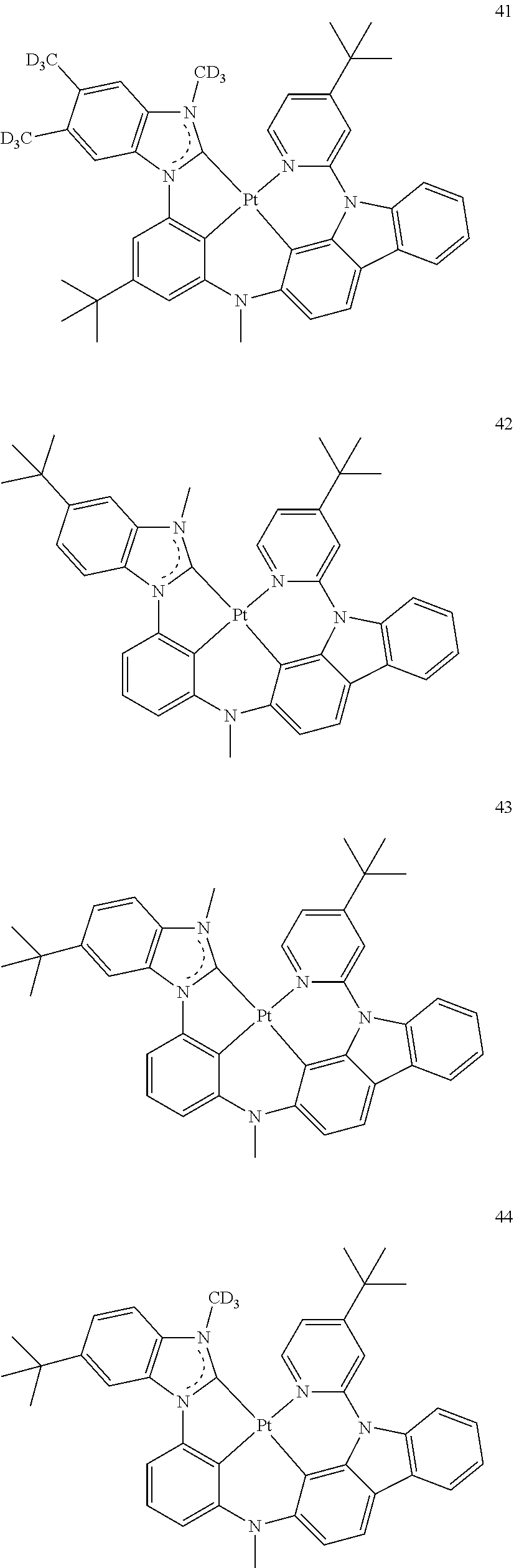


[Hole Transport Region 12]


[Ar601]xe11-[(L601)xe1-R601]xe21. <Formula 601>

—S(═O)2(Q601) or —P(═O)(Q601)(Q602),


| TABLE 1 | |||
| ΔEST | |||
| Compound | (eV) | ||
| S01 | 0.204 | ||
| S02 | 0.218 | ||
| S03 | 0.218 | ||
| PXZ-DPS | 0.028 | ||
    |
|||
| TABLE 2 | |||
| HOMO | |||
| Compounds(Sensitizer) | (eV) | ||
| S01 | −5.46 | ||
| S02 | −5.33 | ||
| S03 | −5.33 | ||
| PXZ-DPS | −5.67 | ||
| FD11 | −5.61 | ||
| FD14 | −5.55 | ||
| FD15 | −5.68 | ||
| FD16 | −5.37 | ||
| FD17 | −5.6 | ||
| FD18 | −5.63 | ||
| FD19 | −5.61 | ||
| FD20 | −5.48 | ||
| FD21 | −5.66 | ||
         |
|||
| TABLE 3 | |||||||
| | Second | Condition | 1 | Condition 2 | |||
| host | host | Sensitizer | Dopant | satisfied/unsatisfied | satisfied/unsatisfied | ||
| Example 1 | H-H104 | HE6-27 | S01 | FD14 | satisfied | satisfied | |
| Example 2 | H-H104 | HE6-27 | S01 | FD15 | satisfied | satisfied | |
| Example 3 | H-H104 | HE6-27 | S01 | FD21 | satisfied | satisfied | |
| Example 4 | H-H104 | HE6-27 | S01 | FD19 | satisfied | satisfied | |
| Example 5 | H-H104 | HE6-27 | S03 | FD20 | satisfied | satisfied | |
| Example 6 | H-H104 | HE6-27 | S03 | FD17 | satisfied | satisfied | |
| Example 7 | H-H104 | HE6-27 | S03 | FD18 | satisfied | satisfied | |
| Example 8 | H-H106 | HE6-28 | S02 | FD11 | satisfied | satisfied | |
| Example 9 | H-H106 | HE6-28 | S02 | FD16 | satisfied | satisfied | |
| Example 10 | H-H106 | HE6-28 | S02 | FD18 | satisfied | satisfied | |
| Example 11 | H-H106 | HE6-28 | S02 | FD15 | satisfied | satisfied | |
| Comparative | H-H104 | HE6-27 | PXZ-DPS | FD11 | unsatisfied | satisfied | |
| Example 1X | |||||||
    |
|||||||
| TABLE 4 | |||||
| Weight ratio | |||||
| First | Second | (First host:Second | |||
| host | host | Dopant | host:Dopant) | ||
| Comparative | H-H104 | HE6-27 | FD14 | 50:50:15 |
| Example 1F | ||||
| Comparative | H-H104 | HE6-27 | FD15 | 50:50:15 |
| Example 2F-1 | ||||
| Comparative | H-H106 | HE6-28 | FD15 | 50:50:15 |
| Example 2F-2 | ||||
| Comparative | H-H106 | HE6-28 | FD16 | 50:50:15 |
| Example 3F | ||||
| Comparative | H-H104 | HE6-27 | FD17 | 50:50:15 |
| Example 4F | ||||
| Comparative | H-H104 | HE6-27 | FD18 | 50:50:15 |
| Example 5F-1 | ||||
| Comparative | H-H106 | HE6-28 | FD18 | 50:50:15 |
| Example 5F-2 | ||||
| Comparative | H-H104 | HE6-27 | FD19 | 50:50:15 |
| Example 6F | ||||
| Comparative | H-H104 | HE6-27 | FD20 | 50:50:15 |
| Example 7F | ||||
| Comparative | H-H104 | HE6-27 | FD21 | 50:50:15 |
| Example 8F | ||||
| Comparative | H-H106 | HE6-28 | FD11 | 50:50:15 |
| Example 9F | ||||
| TABLE 5 | |||||
| Lifespan (T95) | EQE | Roll-off ratio | EL λmax | ||
| (%) | (%) | (%) | (nm) | ||
| Example 1 | 100 | 100 | 0.081 | 457 |
| Example 2 | 305.5 | 140.1 | 0.214 | 458 |
| Example 3 | 360.3 | 133.6 | 0.205 | 459 |
| Example 4 | 238.8 | 122.3 | 0.212 | 458 |
| Example 5 | 432.5 | 141.1 | 8 | 465 |
| Example 6 | 430.9 | 178.3 | 11.3 | 465 |
| Example 7 | 1087.3 | 168.2 | 13.4 | 466 |
| Example 8 | 2586.5 | 179.5 | 9.3 | 467 |
| Example 9 | 1539.6 | 155.8 | 12.1 | 465 |
| Example 10 | 2650.8 | 170.4 | 13.4 | 466 |
| Example 11 | 1716.7 | 160.2 | 14.3 | 465 |
| Comparative | 6.35 | 137.6 | 33 | 534 |
| Example 1X | ||||
| TABLE 6 | |||||
| Lifespan (T95) | EQE | Roll-off ratio | EL λmax | ||
| (%) | (%) | (%) | (nm) | ||
| Comparative | 9.90166 | 55.23702 | 38.9 | 456 |
| Example 1F | ||||
| Comparative | 99.1065 | 59.58239 | 32.7 | 460 |
| Example 2F-1 | ||||
| Comparative | 166.4175 | 61.53499 | 31.3 | 461 |
| Example 2F-2 | ||||
| Comparative | 89.90544 | 60.13544 | 32.4 | 455 |
| Example 3F | ||||
| Comparative | 174.741 | 56.87359 | 36.1 | 456 |
| Example 4F | ||||
| Comparative | 224.0848 | 55.60948 | 34.4 | 469 |
| Example 5F-1 | ||||
| Comparative | 253.8608 | 52.52822 | 29.4 | 469 |
| Example 5F-2 | ||||
| Comparative | 131.4112 | 48.90519 | 29.6 | 461 |
| Example 6F | ||||
| Comparative | 38.64871 | 51.42212 | 40.2 | 469 |
| Example 7F | ||||
| Comparative | 171.655 | 50.59819 | 28.6 | 463 |
| Example 8F | ||||
| Comparative | 206.6682 | 53.99549 | 32.8 | 474 |
| Example 9F | ||||
Claims (19)
0.2 eV≤ΔE ST(S) <Condition 1>
|HOMO(D)−HOMO(S)|<0.5 eV <Condition 2>
M11(L11)n11(L12)n12 <Formula 101>

0.2 eV≤ΔE ST(S)≤0.4 eV <Condition 1-1>
T 1(S)≥2.63 eV <Condition 3>
HOMO(S)≥−6.0 eV <Condition 4>
T 1(H)≥T 1(S)≥S 1(D) <Condition 6>
T 1(H)>T 1(S)>S 1(D) <Condition 5>


0.2 eV≤ΔE ST(S) <Condition 1>
|HOMO(D)−HOMO(S)|<0.5 eV <Condition 2>
0.2 eV≤ΔE ST(S) <Condition 1>
|HOMO(D)−HOMO(S)|<0.5 eV <Condition 2>
Applications Claiming Priority (2)
| Application Number | Priority Date | Filing Date | Title |
|---|---|---|---|
| KR10-2019-0157676 | 2019-11-29 | ||
| KR1020190157676A KR20210067752A (en) | 2019-11-29 | 2019-11-29 | Organic light emitting device |
Publications (2)
| Publication Number | Publication Date |
|---|---|
| US20210167311A1 US20210167311A1 (en) | 2021-06-03 |
| US11539012B2 true US11539012B2 (en) | 2022-12-27 |
Family
ID=76091172
Family Applications (1)
| Application Number | Title | Priority Date | Filing Date |
|---|---|---|---|
| US16/944,248 Active 2040-11-06 US11539012B2 (en) | 2019-11-29 | 2020-07-31 | Organic light-emitting device |
Country Status (2)
| Country | Link |
|---|---|
| US (1) | US11539012B2 (en) |
| KR (1) | KR20210067752A (en) |
Families Citing this family (1)
| Publication number | Priority date | Publication date | Assignee | Title |
|---|---|---|---|---|
| KR20240019643A (en) | 2022-08-04 | 2024-02-14 | 삼성전자주식회사 | Display apparatus |
Citations (11)
| Publication number | Priority date | Publication date | Assignee | Title |
|---|---|---|---|---|
| KR20160100961A (en) | 2013-12-20 | 2016-08-24 | 바스프 에스이 | Highly efficient oled devices with very short decay times |
| KR20160101519A (en) | 2015-02-17 | 2016-08-25 | 서울대학교산학협력단 | Organic light-emitting device comprising delayed fluorescent host, phosphorescent dopant and fluorescent dopant |
| US20160329512A1 (en) * | 2013-03-29 | 2016-11-10 | Kyushu University National University Corporation | Organic electroluminescent device |
| KR20170055535A (en) | 2014-09-16 | 2017-05-19 | 시노라 게엠베하 | Light―emitting layer suitable for bright luminescence |
| US20170271610A1 (en) * | 2016-03-18 | 2017-09-21 | Semiconductor Energy Laboratory Co., Ltd. | Light-emitting element, display device, electronic device, and lighting device |
| JP2017197481A (en) | 2016-04-28 | 2017-11-02 | コニカミノルタ株式会社 | π-CONJUGATED COMPOUND, ORGANIC ELECTROLUMINESCENT ELEMENT MATERIAL, LIGHT-EMITTING MATERIAL, CHARGE TRANSPORT MATERIAL, LUMINESCENT THIN FILM, ORGANIC ELECTROLUMINESCENT ELEMENT, DISPLAY DEVICE, AND LIGHTING DEVICE |
| KR20180014738A (en) | 2015-06-03 | 2018-02-09 | 유디씨 아일랜드 리미티드 | High efficiency OLED devices with very short decay time |
| KR20200115134A (en) | 2019-03-29 | 2020-10-07 | 삼성전자주식회사 | Organic light emitting device |
| US20200321537A1 (en) | 2019-03-29 | 2020-10-08 | Samsung Electronics Co., Ltd. | Organic light-emitting device |
| US20200343469A1 (en) * | 2017-11-02 | 2020-10-29 | Semiconductor Energy Laboratory Co., Ltd. | Light-Emitting Element, Display Device, Electronic Device, and Lighting Device |
| US20210202864A1 (en) * | 2018-08-23 | 2021-07-01 | Kyushu University, National University Corporation | Organic electroluminescence element |
-
2019
- 2019-11-29 KR KR1020190157676A patent/KR20210067752A/en active Pending
-
2020
- 2020-07-31 US US16/944,248 patent/US11539012B2/en active Active
Patent Citations (15)
| Publication number | Priority date | Publication date | Assignee | Title |
|---|---|---|---|---|
| US20160329512A1 (en) * | 2013-03-29 | 2016-11-10 | Kyushu University National University Corporation | Organic electroluminescent device |
| KR20160100961A (en) | 2013-12-20 | 2016-08-24 | 바스프 에스이 | Highly efficient oled devices with very short decay times |
| US20200044165A1 (en) | 2013-12-20 | 2020-02-06 | Udc Ireland Limited | Highly efficient oled devices with very short decay times |
| KR20170055535A (en) | 2014-09-16 | 2017-05-19 | 시노라 게엠베하 | Light―emitting layer suitable for bright luminescence |
| US20170250363A1 (en) | 2014-09-16 | 2017-08-31 | Cynora Gmbh | Light-emitting layer suitable for bright luminescence |
| US10418573B2 (en) | 2015-02-17 | 2019-09-17 | Seoul National University R&Db Foundation | Organic light-emitting device comprising host, phosphorescent dopant and fluorescent dopant |
| KR20160101519A (en) | 2015-02-17 | 2016-08-25 | 서울대학교산학협력단 | Organic light-emitting device comprising delayed fluorescent host, phosphorescent dopant and fluorescent dopant |
| KR20180014738A (en) | 2015-06-03 | 2018-02-09 | 유디씨 아일랜드 리미티드 | High efficiency OLED devices with very short decay time |
| US20180182980A1 (en) | 2015-06-03 | 2018-06-28 | Udc Ireland Limited | Highly efficient oled devices with very short decay times |
| US20170271610A1 (en) * | 2016-03-18 | 2017-09-21 | Semiconductor Energy Laboratory Co., Ltd. | Light-emitting element, display device, electronic device, and lighting device |
| JP2017197481A (en) | 2016-04-28 | 2017-11-02 | コニカミノルタ株式会社 | π-CONJUGATED COMPOUND, ORGANIC ELECTROLUMINESCENT ELEMENT MATERIAL, LIGHT-EMITTING MATERIAL, CHARGE TRANSPORT MATERIAL, LUMINESCENT THIN FILM, ORGANIC ELECTROLUMINESCENT ELEMENT, DISPLAY DEVICE, AND LIGHTING DEVICE |
| US20200343469A1 (en) * | 2017-11-02 | 2020-10-29 | Semiconductor Energy Laboratory Co., Ltd. | Light-Emitting Element, Display Device, Electronic Device, and Lighting Device |
| US20210202864A1 (en) * | 2018-08-23 | 2021-07-01 | Kyushu University, National University Corporation | Organic electroluminescence element |
| KR20200115134A (en) | 2019-03-29 | 2020-10-07 | 삼성전자주식회사 | Organic light emitting device |
| US20200321537A1 (en) | 2019-03-29 | 2020-10-08 | Samsung Electronics Co., Ltd. | Organic light-emitting device |
Non-Patent Citations (16)
| Title |
|---|
| ADF2009.01, SCM, Theoretical Chemistry, Vrije Universiteit, Amsterdam, The Netherlands, 2010. |
| Ansgar Schafer, et al., Fully optimized contracted Gaussian basis sets for atoms Li to Kr, J. Chern. Phys. 97 (4), Aug. 15, 1992, 2571-2577. |
| Axel D. Becke, Density-functional thermochemistry. III. The role of exact exchange, J. Chern. Phys. 98 (7). Apr. 1, 1993. |
| D. Andrae, et al., Energy-adjusted ab initio pseudopotentials for the second and third row transition elements, Theor Chim Acta (1990) 77: 123-141. |
| E. Van Lenthe, et al., Optimized Slater-Type Basis Sets for the Elements 1-118, 2003 Wiley Periodicals, Inc. J Comput Chem 24: 1142-1156, 2003. |
| English Abstract of JP 2017-197481. |
| Erik van Lenthe, et al., Geometry optimizations in the zero order regular approximation for relativistic effects, Journal of Chemical Physics vol. 110, No. 18 May 8, 1999. |
| Fan Wang, et al., A simplified relativistic time-dependent density-functional theory formalism for the calculations of excitation energies including spin-orbit coupling effect, The Journal of Chemical Physics 123, 154102 (2005). |
| Hyun-Gu Kim, et al., Harnessing Triplet Excited States by Fluorescent Dopant Utilizing Codoped Phosphorescent Dopant in Exciplex Host for Efficient Fluorescent Organic Light Emitting Diodes, Adv. Optical Mater. 2017, 1600749 (6 pp.). |
| John P. Perdew, Department of Physics and Quantum Theory GroupT, Ulane University Density-functional approximation for the correlation energy of the inhomogeneous electron gas, Physical Review B, vol. 33, No. 12, Jun. 15, 1986. |
| Lindsay E. Roy, et al., Revised Basis Sets for the LANL Effective Core Potentials, J. Chem. Theory Comput. 2008, 4, 1029-1031. |
| R. Ahlrichs, M. Bar, M. Haser, H. Hom, and C. Colmel, Electronic Structure Calculations on Workstation Computers: The Program System Turbomole, Chem. Phys.Lett. 162, 165-169 (1989). |
| Shiyong Liu, et al., Enhanced red emission from fluorescent organic light-emitting devices utilizing a phosphorescent sensitizer, Japanese Journal of Applied Physics vol. 43, No. 4B, 2004, pp. 2320-2322. |
| Sinheui Kim, et al., Degradation of blue-phosphorescent organic light-emitting devices involves exciton-induced generation of polaron pair within emitting layers, Nature Communications, DOI: 10.1038/s41467-018-03602-4. |
| Tengxiao Liu, et al. Boosting the Efficiency of Near-Infrared Fluorescent OLEDs with an Electroluminescent Peak of Nearly 800 nm by Sensitizer-Based Cascade Energy Transfer, Adv. Funct. Mater. 2018, 1706088 (8 pp). |
| W. J. Hehre, et al., Self-Consistent Molecular Orbital Methods. XII. Further Extensions of Gaussian-Type Basis Sets for Use in Molecular Orbital Studies of Organic Molecules, J. Chem. Phys. 56, 2257 (1972); doi: 10.1063/1.1677527. |
Also Published As
| Publication number | Publication date |
|---|---|
| US20210167311A1 (en) | 2021-06-03 |
| KR20210067752A (en) | 2021-06-08 |
Similar Documents
| Publication | Publication Date | Title |
|---|---|---|
| US12415951B2 (en) | Organic light-emitting device | |
| US20200321537A1 (en) | Organic light-emitting device | |
| US20230132356A2 (en) | Organic light-emitting device | |
| US20180248127A1 (en) | Condensed cyclic compound and organic light-emitting device including the same | |
| US12297214B2 (en) | Condensed cyclic compound, organic light-emitting device including the same, and electronic apparatus including the organic light-emitting device | |
| US12063804B2 (en) | Organic light-emitting device | |
| US20230090659A1 (en) | Organic light-emitting device | |
| US11925115B2 (en) | Organic light-emitting device comprising emission layer satisfying specific singlet excitation energy level conditions | |
| US20230174560A1 (en) | Heterocyclic compound, organic light-emitting device including the same, and electronic apparatus including the organic light-emitting device | |
| US20210284906A1 (en) | Organic light-emitting device | |
| US20230165130A1 (en) | Heterocyclic compound, organic light-emitting device including the heterocyclic compound, and electronic apparatus including the organic light-emitting device | |
| US20230080626A1 (en) | Condensed cyclic compound, organic light-emitting device including the same, and electronic apparatus including the organic light-emitting device | |
| US11453628B2 (en) | Condensed cyclic compound, composition including the same, and organic light-emitting device including thin film formed from the composition | |
| US20170179204A1 (en) | Organic light-emitting device | |
| US20230081897A1 (en) | Polycyclic compound and organic light-emitting device including the same | |
| US11539012B2 (en) | Organic light-emitting device | |
| US11124533B2 (en) | Organometallic compound and organic light-emitting device including the same | |
| US12048243B2 (en) | Organic light-emitting device | |
| US12122749B2 (en) | Heterocyclic compound and organic light-emitting device comprising same | |
| US20200055886A1 (en) | Organometallic compound and organic light-emitting device including the same | |
| US20230078199A1 (en) | Composition and organic light-emitting device including the same | |
| US20230189644A1 (en) | Organic light-emitting device and apparatus including the same | |
| US20230301179A1 (en) | Heterocyclic compound, organic light-emitting device including the same, and electronic apparatus including the organic light-emitting device | |
| US12114563B2 (en) | Organic light-emitting device | |
| US11800801B2 (en) | Organic light-emitting device |
Legal Events
| Date | Code | Title | Description |
|---|---|---|---|
| FEPP | Fee payment procedure |
Free format text: ENTITY STATUS SET TO UNDISCOUNTED (ORIGINAL EVENT CODE: BIG.); ENTITY STATUS OF PATENT OWNER: LARGE ENTITY |
|
| AS | Assignment |
Owner name: SAMSUNG ELECTRONICS CO., LTD., KOREA, REPUBLIC OF Free format text: ASSIGNMENT OF ASSIGNORS INTEREST;ASSIGNORS:JEON, SOONOK;KWON, EUNSUK;KIM, SANGMO;AND OTHERS;REEL/FRAME:053392/0937 Effective date: 20200716 |
|
| STPP | Information on status: patent application and granting procedure in general |
Free format text: APPLICATION DISPATCHED FROM PREEXAM, NOT YET DOCKETED |
|
| STPP | Information on status: patent application and granting procedure in general |
Free format text: DOCKETED NEW CASE - READY FOR EXAMINATION |
|
| STPP | Information on status: patent application and granting procedure in general |
Free format text: NON FINAL ACTION MAILED |
|
| STPP | Information on status: patent application and granting procedure in general |
Free format text: RESPONSE TO NON-FINAL OFFICE ACTION ENTERED AND FORWARDED TO EXAMINER |
|
| STPP | Information on status: patent application and granting procedure in general |
Free format text: NOTICE OF ALLOWANCE MAILED -- APPLICATION RECEIVED IN OFFICE OF PUBLICATIONS |
|
| STPP | Information on status: patent application and granting procedure in general |
Free format text: NOTICE OF ALLOWANCE MAILED -- APPLICATION RECEIVED IN OFFICE OF PUBLICATIONS |
|
| STPP | Information on status: patent application and granting procedure in general |
Free format text: PUBLICATIONS -- ISSUE FEE PAYMENT RECEIVED |
|
| STPP | Information on status: patent application and granting procedure in general |
Free format text: PUBLICATIONS -- ISSUE FEE PAYMENT VERIFIED |
|
| STCF | Information on status: patent grant |
Free format text: PATENTED CASE |