US11527954B2 - Regulator circuit and front end module including the same - Google Patents
Regulator circuit and front end module including the same Download PDFInfo
- Publication number
- US11527954B2 US11527954B2 US17/210,573 US202117210573A US11527954B2 US 11527954 B2 US11527954 B2 US 11527954B2 US 202117210573 A US202117210573 A US 202117210573A US 11527954 B2 US11527954 B2 US 11527954B2
- Authority
- US
- United States
- Prior art keywords
- transistor
- output voltage
- terminal
- voltage
- output
- Prior art date
- Legal status (The legal status is an assumption and is not a legal conclusion. Google has not performed a legal analysis and makes no representation as to the accuracy of the status listed.)
- Active, expires
Links
Images


Classifications
-
- G—PHYSICS
- G05—CONTROLLING; REGULATING
- G05F—SYSTEMS FOR REGULATING ELECTRIC OR MAGNETIC VARIABLES
- G05F1/00—Automatic systems in which deviations of an electric quantity from one or more predetermined values are detected at the output of the system and fed back to a device within the system to restore the detected quantity to its predetermined value or values, i.e. retroactive systems
- G05F1/10—Regulating voltage or current
- G05F1/46—Regulating voltage or current wherein the variable actually regulated by the final control device is DC
- G05F1/56—Regulating voltage or current wherein the variable actually regulated by the final control device is DC using semiconductor devices in series with the load as final control devices
-
- H—ELECTRICITY
- H02—GENERATION; CONVERSION OR DISTRIBUTION OF ELECTRIC POWER
- H02M—APPARATUS FOR CONVERSION BETWEEN AC AND AC, BETWEEN AC AND DC, OR BETWEEN DC AND DC, AND FOR USE WITH MAINS OR SIMILAR POWER SUPPLY SYSTEMS; CONVERSION OF DC OR AC INPUT POWER INTO SURGE OUTPUT POWER; CONTROL OR REGULATION THEREOF
- H02M3/00—Conversion of DC power input into DC power output
- H02M3/02—Conversion of DC power input into DC power output without intermediate conversion into AC
- H02M3/04—Conversion of DC power input into DC power output without intermediate conversion into AC by static converters
- H02M3/10—Conversion of DC power input into DC power output without intermediate conversion into AC by static converters using discharge tubes with control electrode or semiconductor devices with control electrode
- H02M3/145—Conversion of DC power input into DC power output without intermediate conversion into AC by static converters using discharge tubes with control electrode or semiconductor devices with control electrode using devices of a triode or transistor type requiring continuous application of a control signal
- H02M3/155—Conversion of DC power input into DC power output without intermediate conversion into AC by static converters using discharge tubes with control electrode or semiconductor devices with control electrode using devices of a triode or transistor type requiring continuous application of a control signal using semiconductor devices only
-
- H—ELECTRICITY
- H03—ELECTRONIC CIRCUITRY
- H03K—PULSE TECHNIQUE
- H03K19/00—Logic circuits, i.e. having at least two inputs acting on one output; Inverting circuits
- H03K19/20—Logic circuits, i.e. having at least two inputs acting on one output; Inverting circuits characterised by logic function, e.g. AND, OR, NOR, NOT circuits
-
- H—ELECTRICITY
- H02—GENERATION; CONVERSION OR DISTRIBUTION OF ELECTRIC POWER
- H02M—APPARATUS FOR CONVERSION BETWEEN AC AND AC, BETWEEN AC AND DC, OR BETWEEN DC AND DC, AND FOR USE WITH MAINS OR SIMILAR POWER SUPPLY SYSTEMS; CONVERSION OF DC OR AC INPUT POWER INTO SURGE OUTPUT POWER; CONTROL OR REGULATION THEREOF
- H02M1/00—Details of apparatus for conversion
- H02M1/32—Means for protecting converters other than automatic disconnection
-
- H—ELECTRICITY
- H02—GENERATION; CONVERSION OR DISTRIBUTION OF ELECTRIC POWER
- H02M—APPARATUS FOR CONVERSION BETWEEN AC AND AC, BETWEEN AC AND DC, OR BETWEEN DC AND DC, AND FOR USE WITH MAINS OR SIMILAR POWER SUPPLY SYSTEMS; CONVERSION OF DC OR AC INPUT POWER INTO SURGE OUTPUT POWER; CONTROL OR REGULATION THEREOF
- H02M3/00—Conversion of DC power input into DC power output
- H02M3/02—Conversion of DC power input into DC power output without intermediate conversion into AC
- H02M3/04—Conversion of DC power input into DC power output without intermediate conversion into AC by static converters
- H02M3/10—Conversion of DC power input into DC power output without intermediate conversion into AC by static converters using discharge tubes with control electrode or semiconductor devices with control electrode
- H02M3/145—Conversion of DC power input into DC power output without intermediate conversion into AC by static converters using discharge tubes with control electrode or semiconductor devices with control electrode using devices of a triode or transistor type requiring continuous application of a control signal
- H02M3/155—Conversion of DC power input into DC power output without intermediate conversion into AC by static converters using discharge tubes with control electrode or semiconductor devices with control electrode using devices of a triode or transistor type requiring continuous application of a control signal using semiconductor devices only
- H02M3/156—Conversion of DC power input into DC power output without intermediate conversion into AC by static converters using discharge tubes with control electrode or semiconductor devices with control electrode using devices of a triode or transistor type requiring continuous application of a control signal using semiconductor devices only with automatic control of output voltage or current, e.g. switching regulators
-
- H—ELECTRICITY
- H02—GENERATION; CONVERSION OR DISTRIBUTION OF ELECTRIC POWER
- H02J—ELECTRIC POWER NETWORKS; CIRCUIT ARRANGEMENTS OR SYSTEMS FOR SUPPLYING OR DISTRIBUTING ELECTRIC POWER; SYSTEMS FOR STORING ELECTRIC ENERGY
- H02J2207/00—Details of circuit arrangements for charging or discharging batteries or supplying loads from batteries
- H02J2207/10—Control circuit supply, e.g. means for supplying power to the control circuit
Definitions
- the following description relates to a regulator circuit and a front end module including the same.
- a front-end module integrated circuit (e.g., a WiFi front-end module IC) has been developing at a rapid pace every year with the trend of miniaturization and low power consumption.
- a power management IC (PMIC) was used as a power source for the front-end module IC.
- the PMIC serves to supply a constant voltage and current.
- a method of directly using a battery of a communication device is changing without using a PMIC depending on a trend of miniaturization and low power consumption.
- a battery of the communication device may have a voltage change of, e.g., a voltage change of about 3.0 V to 4.6 V. Such a voltage change may have a significant impact on the performance of a front-end module, and may cause damage to circuits and components inside the front-end module IC.
- a regulator circuit includes: a first output voltage generator configured to include a first resistor having a first end connected to a power terminal having externally supplied power, a first transistor connected between a second end of the first resistor and a ground terminal to supply a first voltage, and a second transistor receiving the first voltage through a control terminal of the second transistor and outputting a first output voltage through a first terminal of the second transistor; and a second output voltage generator connected between the power terminal and the first output voltage generator to output a second output voltage obtained by adding a predetermined voltage into the first output voltage.
- the second output voltage generator may include: a second resistor connected between the power terminal and the first resistor; and a third transistor configured to receive a second voltage obtained by adding a voltage across the first resistor into the first voltage through a control terminal of the third transistor, and to output the second output voltage through a first terminal of the third transistor.
- a second terminal of the third transistor may be connected to the power terminal, and a first terminal of the third transistor may be connected to a second terminal of the second transistor.
- the first output voltage generator may further include a second resistor connected between the first terminal of the second transistor and the ground terminal.
- the first output voltage generator may further include a third transistor configured to have a control terminal of the third transistor connected to the control terminal of the first transistor, a first terminal of the third transistor connected to the second resistor, and a second terminal of the third transistor connected to the first terminal of the second transistor.
- a control terminal and a first terminal of the first transistor may be connected to each other, the first terminal of the first transistor may be connected to the second end of the first resistor, and a second terminal of the first transistor may be connected to the ground terminal.
- the first transistor may include a plurality of transistors having a diode-connection structure, and the plurality of transistors may supply the first voltage to the control terminal of the second transistor.
- the regulator circuit may include: a third output voltage generator configured to include a third resistor connected between the power and the second resistor; and a fourth transistor configured to receive a third voltage obtained by adding a voltage across the second resistor into the second voltage through a control terminal and to output a third output voltage through a first terminal.
- the first transistor may include a plurality of transistors having a diode-connection structure, and the plurality of transistors may supply the first voltage to the control terminal of the second transistor.
- the regulator circuit may further include a third output voltage generator configured to include a third resistor connected between the power terminal and the second resistor, and a fourth transistor configured to receive a third voltage obtained by adding a voltage across the second resistor into the second voltage through a control terminal of the fourth transistor, and output a third output voltage through a first terminal of the fourth transistor.
- a third output voltage generator configured to include a third resistor connected between the power terminal and the second resistor
- a fourth transistor configured to receive a third voltage obtained by adding a voltage across the second resistor into the second voltage through a control terminal of the fourth transistor, and output a third output voltage through a first terminal of the fourth transistor.
- the third output voltage may be higher than the second output voltage.
- the power of the power terminal may be supplied from a battery.
- a regulator circuit in another general aspect, includes a first resistor, a second resistor, a first transistor, a second transistor, a third transistor, and a third resistor.
- the first resistor is configured to have a first end connected to a power terminal.
- the second resistor is configured to have a first end connected to a second end of the first resistor.
- the first transistor connected between a second end of the second resistor and a ground terminal, is configured to supply a first voltage.
- the second transistor is configured to receive the first voltage through a control terminal, and output the first output voltage through a first terminal.
- the third transistor is configured to receive a second voltage obtained by adding a voltage across the second resistor into the first voltage through a control terminal of the third transistor, and output a second output voltage through a first terminal of the third transistor.
- the third resistor is connected between the first terminal of the second transistor and the ground terminal.
- the control terminal and a first terminal of the first transistor may be connected to each other.
- the second terminal of the third transistor may be connected to the power terminal, and the first terminal of the third transistor may be connected to a second terminal of the second transistor.
- the regulator circuit may further include a fourth transistor configured to have a control terminal connected to the control terminal of the first transistor, a first terminal connected to the third resistor, and a second terminal connected to the first terminal of the second transistor.
- the first transistor may have a diode-connection structure and may include a plurality of transistors stacked between the second end of the second resistor and the ground terminal.
- the plurality of transistors may supply the first voltage to a control terminal of the first transistor.
- the regulator circuit may further include a fourth resistor connected between the power terminal and the first resistor, and a fourth transistor configured to receive a third voltage obtained by adding a voltage across the first resistor into the second voltage through a control terminal of the fourth transistor, and output a third output voltage through a first terminal of the fourth transistor.
- the second output voltage may be higher than the first output voltage, and the third output voltage is higher than the second output voltage.
- a front-end module include a regulator and an inverter unit.
- the regulator is configured to include a first output voltage generator connected between a power terminal and a ground terminal to output a first output voltage, and a second output voltage generator connected between the power terminal and the first output voltage generator to output a second output voltage obtained by adding a predetermined voltage into the first output voltage.
- the inverter unit includes a first inverter configured to operate by receiving the first output voltage to output the first output voltage in response to an input signal, and a second inverter configured to operate by receiving the second output voltage to output the second output voltage in response to an output signal of the first inverter.
- the regulator circuit may further include a third output voltage generator connected between the power terminal and the second output voltage generator to output a third output voltage obtained by adding a predetermined voltage into the second output voltage.
- the inverter unit may further include a third inverter configured to operate by receiving the third output voltage to output the third output voltage in response to an output signal of the second inverter.
- the second output voltage may be equal to or higher than a voltage obtained by subtracting a threshold voltage of a transistor included in the third inverter from the third output voltage.
- FIG. 1 illustrates an example of a front-end module.
- FIG. 2 illustrates an example of a controller
- FIG. 3 illustrates an example of a regulator circuit.
- FIG. 4 illustrates an example of a circuit diagram showing a specific configuration of a regular circuit.
- FIG. 5 illustrates another example of a circuit diagram showing a specific configuration of a regulator circuit.
- FIG. 6 illustrates another example of a circuit diagram showing a specific configuration of a regulator circuit.
- FIG. 7 illustrates another example of a circuit diagram showing a specific configuration of a regulator circuit.
- FIG. 8 A and FIG. 8 B illustrate simulation results of the regulator circuit of FIG. 7 .
- FIG. 9 illustrates an application example of a regulator circuit.
- first,” “second,” and “third” may be used herein to describe various members, components, regions, layers, or sections, these members, components, regions, layers, or sections are not to be limited by these terms. Rather, these terms are only used to distinguish one member, component, region, layer, or section from another member, component, region, layer, or section. Thus, a first member, component, region, layer, or section referred to in examples described herein may also be referred to as a second member, component, region, layer, or section without departing from the teachings of the examples.
- spatially relative terms such as “above,” “upper,” “below,” and “lower” may be used herein for ease of description to describe one element's relationship to another element as shown in the figures. Such spatially relative terms are intended to encompass different orientations of the device in use or operation in addition to the orientation depicted in the figures. For example, if the device in the figures is turned over, an element described as being “above” or “upper” relative to another element will then be “below” or “lower” relative to the other element. Thus, the term “above” encompasses both the above and below orientations depending on the spatial orientation of the device.
- the device may also be oriented in other ways (for example, rotated 90 degrees or at other orientations), and the spatially relative terms used herein are to be interpreted accordingly.
- RF signals may include Wi-Fi (IEEE 802.11 family, etc.), WiMAX (IEEE 802.16 family, etc.), IEEE 802.20, LTE (long term evolution), Ev-DO, HSPA+, HSDPA+, HSUPA+, EDGE, GSM, GPS, GPRS, CDMA, TDMA, DECT, Bluetooth, 3G, 4G, 5G, and any other wireless and wired protocols designated thereafter, but the present invention is limited thereto.
- FIG. 1 illustrates an example of a front-end module.
- the front end module 1000 may include a controller 100 , a low noise amplifier 200 , and a switch unit 300 .
- the front-end module 1000 may receive a power VDD from an external source and be operated by the received power VDD.
- the power VDD may be supplied from a battery of a communication device in which the front-end module 1000 is mounted. That is, the front-end module 1000 may operate by receiving power VDD directly from the battery.
- the power VDD supplied from the battery may have a voltage of 3.0 to 4.6 V.
- the front-end module 1000 may be implemented as one integrated circuit (IC).
- the controller 100 serves to control the low noise amplifier 200 and the switch unit 300 .
- the controller 100 may control operations of transistors included in the low noise amplifier 200 .
- the controller 100 may control the operations of the transistors included in the switch unit 300 .
- the controller 100 may convert a voltage supplied from the power VDD into a regulating voltage to supply the regulating voltage to the low noise amplifier 200 and/or the switch unit 300 .
- the low noise amplifier 200 may amplify a received radio frequency RF under the control of the controller 100 .
- the low noise amplifier 200 may receive a regulating voltage as a bias (operation) voltage from the controller 100 .
- the switch unit 300 may include a plurality of switches, and may selectively switch a transmission RF signal and a reception RF signal under the control of the controller 100 .
- the switch unit 300 may receive a regulating voltage as a bias (operation) voltage from the controller 100 .
- FIG. 2 illustrates an example of a controller
- the controller 100 may include a regulator circuit 110 and a decoder 120 .
- the regulator circuit 110 receives the power VDD externally supplied and converts the received power VDD into a predetermined regulating voltage Vout.
- the regulating voltage Vout may be supplied to the low noise amplifier 200 and/or the switch unit 300 .
- the regulating voltage Vout may be supplied (input) to the decoder 120 .
- the regulator circuit 110 may generate and output a plurality of regulating voltages (e.g., Vout 1 and Vout 2 ) as the regulating voltage Vout.
- Vout 1 and Vout 2 regulating voltages
- the decoder 120 receives an external control bit to generate a switching signal in response to the control bit.
- the decoder 120 may output the generated switching signal to the switch unit 300 .
- the switch unit 300 may turn on or turn off a switch included therein in response to the switching signal that is inputted from the decoder 120 .
- the decoder 120 may receive a regulating voltage Vout as operating power from the regulator circuit 110 .
- the decoder 120 may include a logic circuit and an inverter, and the logic circuit and the inverter may be biased by the regulating voltage Vout. With reference to FIG. 9 below, an example in which the regulating voltage Vout is applied to an inverter chain will be described, but the regulating voltage Vout may be used as power that is supplied for other circuit elements.
- FIG. 3 illustrates an example of a regulator circuit.
- the regulator circuit 110 may include a first output voltage generator 111 and a second output voltage generator 112 .
- the first output voltage generator 111 may be connected between the power VDD and ground to generate and output the first output voltage Vout 1 .
- the first output voltage Vout 1 corresponds to a regulating voltage of the regulator circuit 110 .
- the second output voltage generator 112 may be connected between the power VDD and the first output voltage generator 111 to generate and output a second output voltage Vout 2 , a voltage obtained by adding a predetermined voltage to the first output voltage Vout.
- the second output voltage Vout 2 also corresponds to the regulating voltage of the regulator circuit 110 .
- the regulator circuit 110 may generate and output the first output voltage Vout 1 and the second output voltage Vout 2 , a plurality of regulating voltages.
- FIG. 4 illustrates an example of a circuit diagram showing a specific configuration of a regular circuit.
- the regulator circuit 110 a may include a first output voltage generator 111 a and a second output voltage generator 112 a.
- the first output voltage generator 111 a may include a transistor M 1 , a transistor M 3 , a resistor R 2 , and a resistor R 3 .
- the second output voltage generator 112 a may include a resistor R 1 and a transistor M 2 .
- a gate and a drain of the transistor M 1 are connected to each other, and a source of the transistor M 1 is connected to a ground. That is, the transistor M 1 has a diode-connection structure.
- a gate of the transistor M 3 is connected to the drain of the transistor M 1 , and a first end of the resistor R 2 is connected to the drain of the transistor M 1 and the gate of the transistor M 3 .
- the resistor R 3 is connected between a source of the transistor M 3 and the ground.
- the resistor R 1 is connected between the power VDD and a second end of the resistor R 2 .
- the gate of the transistor M 2 is connected to a contact point between the resistor R 1 and the resistor R 2 , and a drain of the transistor M 2 is connected to the power VDD.
- a source of the transistor M 2 is connected to the drain of the transistor M 3 .
- the transistors M 1 , M 2 , and M 3 may be a field effect transistor (FET), a metal oxide semiconductor field effect transistor (MOSFET), a bipolar junction transistor (BJT), or the like. Further, other transistors described below may also be a FET, a MOSFET, or a BJT.
- FET field effect transistor
- MOSFET metal oxide semiconductor field effect transistor
- BJT bipolar junction transistor
- other transistors described below may also be a FET, a MOSFET, or a BJT.
- a source voltage of the transistor M 3 corresponds to the first output voltage Vout 1
- a source voltage of the transistor M 2 corresponds to the second output voltage Vout 2
- a drain-source voltage of the transistor M 1 is represented as Vds 1
- a gate voltage of the transistor M 3 is represented as Vg 3
- a gate-source voltage of the transistor M 3 is represented as Vgs 3
- a voltage across the resistor R 2 is represented as VR 2
- a gate voltage of the transistor M 2 is represented as Vg 2
- a gate-source voltage of the transistor M 2 is represented as Vgs 2 .
- the drain-source voltage Vds 1 of the transistor M 1 corresponds to the gate voltage Vg 3 of the transistor M 3 . Accordingly, the transistor M 1 serves to supply the gate voltage of the transistor M 3 . That is, a relationship of Equation 1 below may be established.
- Vg 3 Vds 1 Equation 1:
- the first output voltage Vout 1 corresponds to a value obtained by subtracting the gate-source voltage Vgs 3 of the transistor M 3 from the gate voltage Vg 3 of the transistor M 3 . That is, a relationship of Equation 2 below may be established for the first output voltage Vout 1 .
- Vds 1 and Vgs 3 are determined depending on the design process of the transistors M 1 and M 3 .
- the second output voltage Vout 2 corresponds to a value obtained by subtracting the gate-source voltage Vgs 2 of the transistor M 2 from the gate voltage Vg 2 of the transistor M 2 .
- Vds 1 and Vgs 2 are determined depending on the design process of the transistors M 1 and M 2 . Further, in Equation 4, V R2 is determined depending on the magnitude of the current I 1 . Comparing Equation 2 and Equation 4, the second output voltage Vout 2 may have a voltage that is greater than the first output voltage Vout 1 by a predetermined voltage VR 2 ⁇ Vgs 2 +Vgs 3 .
- the first output voltage generator 111 a of the regulator circuit 110 a generates and outputs the first output voltage Vout 1 .
- the second output voltage generator 112 a of the regulator circuit 110 a generates and outputs the second output voltage Vout 2 , which is a predetermined voltage that is added into the first output voltage Vout.
- the second output voltage Vout 2 is lower than a voltage of the power VDD.
- the currents I 1 and I 2 decrease as the values of the resistors R 1 and R 2 and R 3 are larger, it may be advantageous that the values of the resistors R 1 and R 2 and the resistor R 3 are larger in order to reduce a consumption current.
- too large values of the resistors R 1 and R 2 and the resistor R 3 may delay a time when the gate voltage Vg 3 of the transistor M 3 has a normal voltage. At least one of the values of the resistors R 1 and R 2 may be greater than the value of the resistor R 3 in consideration of such transient response characteristic.
- the resistor R 3 serves to reduce a change in the transient response characteristic for the value of the first output voltage Vout 1 . Since the resistor R 3 provides a current bypass path between the first output voltage Vout 1 and the ground, it is possible to reduce a change in the transient response characteristic of the first output voltage Vout 1 .
- the first output voltage Vout 1 may vary depending on an external load (e.g., a device that receives Vout 1 ), and the resistor R 3 serves to reduce a variation of the first output voltage Vout. That is, the resistor R 3 may stabilize the first output voltage Vout 1 .
- the regulator circuit may supply a plurality of more stable regulating voltages Vout 1 and Vout 2 even when the power VDD is directly supplied from the battery.
- the power VDD supplied from the battery may have a voltage of 3.0 to 4.6 V, and a transistor included in the decoder 120 may have a drain-source breakdown voltage of 3.5 V.
- the regulator circuit may supply a plurality of regulating voltages that are lower than the drain-source breakdown voltage of the transistor. That is, the front-end module may supply a stable voltage through a regulator circuit positioned therein without an external power management IC (PMIC).
- PMIC external power management IC
- FIG. 5 illustrates another example of a circuit diagram showing a specific configuration of a regulator circuit.
- the regulator circuit 110 b may include a first output voltage generator 111 b and a second output voltage generator 112 b . Since the regulator circuit 110 b of FIG. 5 is the same except that the transistor M 4 is added into the regulator circuit 110 a of FIG. 4 , a duplicate description will be omitted.
- a gate of transistor M 4 is connected to the gate of transistor M 1 , and a drain of transistor M 4 is connected to the source of transistor M 3 .
- the resistor R 3 is connected between a source of the transistor M 4 and the ground.
- the transistor M 4 may provide a current bypass path between the first output voltage Vout 1 and the ground in addition to the resistor R 3 . That is, the transistor M 4 and the resistor R 3 serve to reduce a change in the transient response characteristic of the first output voltage Vout 1 .
- the first output voltage Vout 1 may vary depending on an external load (e.g., a device that receives Vout 1 ), and the transistor M 4 and the resistor R 3 serve to reduce a variation of the first output voltage Vout. That is, the transistor M 4 and the resistor R 3 may stabilize the first output voltage Vout 1 .
- FIG. 6 illustrates another example of a circuit diagram showing a specific configuration of a regulator circuit.
- the regulator circuit 110 c may include a first output voltage generator 111 c and a second output voltage generator 112 c . Since the regulator circuit 110 c of FIG. 6 is the same except that the transistor M 1 is replaced with transistors M 11 , M 12 , and M 13 stacked on top of each other, a duplicate description will be omitted.
- the transistor M 1 serves to supply the gate voltage Vg 3 of the transistor M 3 .
- the transistor M 3 may stack a plurality of transistors, thereby supplying the gate voltage Vg 3 of the transistor M 3 with a higher voltage.
- the regulator circuit 110 c of FIG. 6 is an example in which three transistors M 11 , M 12 , and M 13 are stacked, but two transistors or four or more transistors may be stacked depending on a design.
- a gate and a drain of the transistor M 13 are connected to each other, and a source of the transistor M 13 is connected to a ground.
- a gate and a drain of the transistor M 12 are connected to each other, and a source of the transistor M 12 is connected to the drain of the transistor M 13 .
- Agate and a drain of the transistor M 11 are connected to each other, and a source of the transistor M 11 is connected to the drain of the transistor M 12 .
- the drain of the transistor M 11 is connected to the first end of the resistor R 2 and the gate of the transistor M 3 .
- the transistors M 11 , M 12 , and M 13 each have a diode connection structure, and they are stacked between the gate of the transistor M 3 of and the ground.
- a drain-source voltage of the transistor M 11 is represented as Vds 11
- a drain-source voltage of the transistor M 12 is represented as Vds 12
- a drain-source voltage of the transistor M 13 is represented as Vds 13 . Accordingly, the gate voltage of the transistor M 3 becomes as in Equation 5 below.
- Vds is 0.52 V.
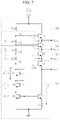
- FIG. 7 a case in which a regulator circuit generates an additional output voltage in addition to the two output voltages Vout 1 and Vout 2 will be described with reference to FIG. 7 .
- FIG. 7 as an example, a case where a regulator circuit generates four output voltages Vout 1 , Vout 2 , Vout 3 , and Vout 4 will be described, but it is possible to generate three output voltages or five or more output voltages.
- FIG. 7 illustrates another example of a circuit diagram showing a specific configuration of a regulator circuit.
- the regulator circuit 110 d may include a first output voltage generator 111 d , a second output voltage generator 112 d , a third output voltage generator 113 d , and a fourth output voltage generator 114 d.
- the first output voltage generator 111 d and the second output voltage generator 112 d of FIG. 7 are similar in structure to the first output voltage generator 111 c and the second output voltage generator 112 c in FIG. 6 , respectively, and thus a detailed description will be omitted.
- the third output voltage generator 113 d may include a resistor R 4 and a transistor M 5 .
- the fourth output voltage generator 114 d may include a resistor R 5 and a transistor M 6 .
- the drain of the resistor R 4 is connected to the first end of the resistor R 1 and the gate of the transistor M 5 .
- the drain of the resistor R 3 is connected to the first end of the resistor R 5 and the gate of the transistor M 6 .
- the gate of the transistor M 5 is connected to a contact point between the resistor R 1 and the resistor R 4 .
- the source of the transistor M 5 is connected to the drain of transistor M 2 , and the drain of transistor M 5 is connected to the source of transistor M 6 .
- the resistor R 5 is connected between the power VDD and a second end of the resistor R 4 .
- the gate of the transistor M 6 is connected to a contact point between the resistor R 4 and the resistor R 5 , and a drain of the transistor M 6 is connected to the power VDD.
- a source of the transistor M 6 is connected to the drain of the transistor M 5 .
- a source voltage of the transistor M 5 corresponds to the third output voltage Vout 3
- a source voltage of the transistor M 6 corresponds to the fourth output voltage Vout 4
- a gate voltage of the transistor M 5 is represented as Vg 5
- a gate voltage of the transistor M 6 is represented as Vg 6
- a gate-source voltage of the transistor M 5 is represented as Vgs 5
- a gate-source voltage of the transistor M 6 is represented as Vgs 6
- a voltage across the resistor R 1 is represented as V R1
- a voltage across the resistor R 4 is represented as V R4 .
- the gate voltage Vg 5 of the transistor M 5 corresponds to a value obtained by adding the voltage VR, across the resistor R 1 into the gate voltage Vg 2 of the transistor M 2 .
- the gate voltage Vg 5 of the transistor M 5 becomes as in Equation 6.
- the third output voltage Vout 3 corresponds to a value obtained by subtracting the gate-source voltage VgsS of the transistor M 5 from the gate voltage Vg 5 of the transistor M 5 .
- Equation 6 a relationship of Equation 7 may be established for third output voltage Vout 3 .
- the third output voltage Vout 3 may have a voltage that is greater than the second output voltage Vout 2 by a predetermined voltage.
- the gate voltage Vg 6 of the transistor M 6 corresponds to a value obtained by adding the voltage V R4 across the resistor R 4 to the gate voltage Vg 5 of the transistor M 5 .
- the gate voltage of the transistor M 6 becomes as in Equation 8.
- Vg 6 3 Vds+V R2 +V R1 +V R4 Equation 8:
- the fourth output voltage Vout 4 corresponds to a value obtained by subtracting the gate-source voltage Vgs 6 of the transistor M 6 from the gate voltage Vg 6 of the transistor M 6 .
- Equation 9 a relationship of Equation 9 may be established for the fourth output voltage Vout 4 .
- the fourth output voltage Vout 4 may have a voltage that is greater than the third output voltage Vout 3 by a predetermined voltage.
- the third output voltage generator 113 d may be connected between the power VDD and the second output voltage generator 112 d , to output a third output voltage Vout 3 obtained by adding a predetermined voltage to the second output voltage Vout 2 .
- the third output voltage generator 114 d may be connected between the power VDD and the third output voltage generator 113 d , to output a fourth output voltage Vout 4 obtained by adding a predetermined voltage to the third output voltage Vout 3 .
- FIG. 8 A and FIG. 8 B illustrate simulation results of the regulator circuits 110 d of FIG. 7 .
- FIG. 8 A illustrates a current I 1 +I 2 obtained by summing the current I 1 and the current 12 depending on a voltage change of the power VDD
- FIG. 8 B illustrates the first to fourth output voltages Vout 1 to Vout 4 depending on the voltage change of the power VDD.
- the value of the resistor R 5 is 300 Kohms
- the value of each of the resistors R 4 , R 1 , R 2 , and R 3 is 100 Kohms.
- the current consumption I 1 +I 2 varies from 2.1 uA to 4.5 uA.
- This consumption current represents a current for a case in which the regulator circuit 110 d is in an idle state.
- the inverter receives an output voltage from a regulator circuit
- the inverter receives an output current from the regulator circuit during a switching operation (ON ⁇ OFF).
- the inverter maintains one state of the switching operation (ON or OFF)
- the regulator circuit enters an idle state because the output current is not supplied from the regulator circuit.
- the regulator circuit has the consumption current I 1 +I 2 in a range of 2.1 uA to 4.5 uA in this standby state, which satisfies a system design specification of 10 uA or less.
- the output voltages Vout 1 to Vout 4 varies from 1.07 V-2.28 V.
- Such output voltages Vout 1 to Vout 4 correspond to a voltage that is lower than a drain-source breakdown voltage of a transistor included in the inverter. Accordingly, the inverter may not be destroyed even when the voltage is supplied from the regulator circuit.
- FIG. 9 illustrates an application example of a regulator circuit.
- the entire circuit of FIG. 9 may be included in the controller 100 of the front-end module.
- the entire circuit of FIG. 9 exemplarily shows a case where a regulator circuit 910 supplies an output voltage to an inverter included in the decoder 120 .
- the regulator circuit 910 may be any one of the regulator circuits 110 a , 110 b , 110 c , and 110 d described in FIG. 4 to FIG. 7 .
- the regulator circuit 910 is the regulator circuit 110 d of FIG. 7 that generates four output voltages.
- the regulator circuit 910 generates four output voltages Vout 1 , Vout 2 , Vout 3 , and Vout 4 as regulating voltages, to supply them to an inverter unit 920 .
- currents supplied from the regulator circuit 910 to the inverter unit 920 are represented as I 3 , I 4 , I 5 , and I 6 .
- the inverter unit 920 may include first to fifth inverters 921 , 922 , 923 , 924 , and 925 . That is, the inverter unit 920 may include an inverter chain in which a plurality of inverters are connected to each other. The inverter unit 920 may receive an input signal Vin having a low voltage to output an output signal having a high voltage. That is, each of the first to fifth inverters 921 , 922 , 923 , 924 , and 925 may output increasingly higher voltages. As an example, an input signal of the inverter unit 920 may have a low voltage as a digital signal.
- the inverter unit 920 may receive such a low voltage to output a switching signal that is a high voltage capable of driving a switch. In addition, the inverter unit 920 receives the output voltages Vout 1 , Vout 2 , Vout 3 , and Vout 4 from the regulator circuit 910 as operating power.
- the first inverter 921 may include two transistors Mp 1 and Mn 1 .
- the transistor Mp 1 may be a p-type transistor, and a source of the transistor Mp 1 receives the first output voltage Vout 1 from the regulator circuit 910 .
- the transistor Mn 1 may be an n-type transistor, and a drain of the transistor Mn 1 is connected to a drain of the transistor Mp 1 .
- a source of the transistor Mn 1 is connected to the ground, and a gate of the transistor Mp 1 and a gate of the transistor Mn 1 are connected to each other.
- An input signal Vin is applied at a contact point between the gate of the transistor Mp 1 and the gate of the transistor Mn 1 .
- the output signal Vout 1 / 0 is outputted at a contact point between the drain of the transistor Mp 1 and the drain of the transistor Mn 1 .
- the input signal Vin may be 0 V or 1.8 V. 0 V corresponds to a low level, and 1.8 V corresponds to a high level.
- the second inverter 922 may include two transistors Mp 2 and Mn 2 .
- the transistor Mp 2 may be a p-type transistor, and a source of the transistor Mp 2 receives the second output voltage Vout 2 from the regulator circuit 910 .
- the transistor Mn 2 may be an n-type transistor, and a drain of the transistor Mn 2 is connected to a drain of the transistor Mp 2 .
- a source of the transistor Mn 2 is connected to the ground, and a gate of the transistor Mp 2 and a gate of the transistor Mn 2 are connected to each other.
- the output signal Vout 1 / 0 of the first inverter 921 is applied as an input signal at a contact point between the gate of the transistor Mp 2 and the gate of the transistor Mn 2 .
- An output signal 0 /Vout 2 is outputted at a contact point between the drain of the transistor Mp 2 and the drain of the transistor Mn 2 .
- the third inverter 923 may include two transistors Mp 3 and Mn 3 .
- the transistor Mp 3 may be a p-type transistor, and a source of the transistor Mp 3 receives the third output voltage Vout 3 from the regulator circuit 910 .
- the transistor Mn 3 may be an n-type transistor, and a drain of the transistor Mn 3 is connected to a drain of the transistor Mp 3 .
- a source of the transistor Mn 3 is connected to the ground, and a gate of the transistor Mp 3 and a gate of the transistor Mn 3 are connected to each other.
- the output signal 0 /Vout 2 of the second inverter 922 is applied as an input signal at a contact point between the gate of the transistor Mp 3 and the gate of the transistor Mn 3 .
- the output signal Vout 3 / 0 is outputted at a contact point between the drain of the transistor Mp 3 and the drain of the transistor Mn 3 .
- the fourth inverter 924 may include two transistors Mp 4 and Mn 4 .
- the transistor Mp 4 may be a p-type transistor, and a source of the transistor Mp 4 receives the fourth output voltage Vout 4 from the regulator circuit 910 .
- the transistor Mn 4 may be an n-type transistor, and a drain of the transistor Mn 4 is connected to a drain of the transistor Mp 4 .
- a source of the transistor Mn 4 is connected to the ground, and a gate of the transistor Mp 4 and a gate of the transistor Mn 4 are connected to each other.
- the output signal Vout 3 / 0 of the third inverter 923 is applied as an input signal at a contact point between the gate of the transistor Mp 4 and the gate of the transistor Mn 4 .
- An output signal 0 /Vout 4 is outputted at a contact point between the drain of the transistor Mp 4 and the drain of the transistor Mn 4 .
- the fifth inverter 925 may include two transistors Mp 5 and Mn 5 .
- the transistor Mp 5 may be a p-type transistor, and a source of the transistor Mp 5 receives the fourth output voltage Vout 4 from the regulator circuit 910 .
- the transistor Mn 5 may be an n-type transistor, and a drain of the transistor Mn 5 is connected to a drain of the transistor Mp 5 .
- a source of the transistor Mn 5 is connected to the ground, and a gate of the transistor Mp 5 and a gate of the transistor Mn 5 are connected to each other.
- the output signal 0 /Vout 4 of the fourth inverter 924 is applied as an input signal at a contact point between the gate of the transistor Mp 5 and the gate of the transistor Mn 5 .
- the output signal Vout 4 / 0 is outputted at a contact point between the drain of the transistor Mp 5 and the drain of the transistor Mn 5 .
- the output signal Vout 4 / 0 of the fifth inverter 925 corresponds to a final output signal of the inverter unit 920 .
- the inverter unit 920 may include an odd number of inverters to invert the input signal Vin, and may be implemented as an inverter chain including five inverters as illustrated in FIG. 9 in order to set a voltage level of the final output signal to be high.
- the transistor Mp 1 Since the first inverter 921 receives 0 V, the transistor Mp 1 is turned on. The first inverter 921 outputs the first output voltage Vout 1 supplied from the regulator circuit 910 by turn-on of the transistor Mp 1
- the transistor Mn 2 Since the second inverter 922 receives Vout 1 , the transistor Mn 2 is turned on. The second inverter 922 outputs 0 V by turn-on of the transistor Mn 2 . Since the third inverter 923 receives 0 V, the transistor Mp 3 is turned on. The third inverter 923 outputs the third output voltage Vout 3 supplied from the regulator circuit 910 by turn-on of the transistor Mp 3 . Since the fourth inverter 924 receives Vout 3 , the transistor Mn 4 is turned on. The fourth inverter 924 outputs 0 V by turn-on of the transistor Mn 4 . In addition, since the fifth inverter 925 receives 0 V, the transistor Mp 5 is turned on. The fifth inverter 925 finally outputs the fourth output voltage Vout 4 supplied from the regulator circuit 910 by turn-on of the transistor Mp 5 .
- the transistor Mn 1 Since the first inverter 921 receives 1.8 V, the transistor Mn 1 is turned on. The first inverter 921 outputs 0 V by turn-on of the transistor Mn 1 . Since the second inverter 922 receives 0 V, the transistor Mp 2 is turned on. The second inverter 922 outputs the second output voltage Vout 2 supplied from the regulator circuit 910 by turn-on of the transistor Mp 2 . Since the third inverter 923 receives Vout 2 , the transistor Mn 3 is turned on. The third inverter 923 outputs 0 V by turn-on of the transistor Mn 3 . Since the fourth inverter 924 receives 0 V, the transistor Mp 4 is turned on.
- the fourth inverter 924 outputs the fourth output voltage Vout 4 supplied from the regulator circuit 910 by turn-on of the transistor Mn 4 .
- the fifth inverter 925 receives Vout 4 , the transistor Mn 5 is turned on.
- the fifth inverter 925 finally outputs 0 V by turn-on of the transistor Mp 5 .
- Equation 10 V out1 ⁇ V out2 ⁇ V out3 ⁇ V out4 ⁇ VDD Equation 10:
- the first output voltage Vout 1 needs to satisfy a relationship of Equation 11 in order to prevent an abnormal operation of the first inverter 921 .
- Vth_Mp 1 represents a threshold voltage of the transistor Mp 1
- Vin_max represents a maximum voltage value of the input signal Vin of the first inverter.
- Equation 11 may be equally applied to the second to fifth inverters 922 to 925 . Accordingly, the second to fourth output voltages Vout 2 to Vout 4 also need to satisfy a relationship of Equation 12 in order to prevent the abnormal operation of the second to fifth inverters 922 to 925 .
- Vth_Mp 2 , Vth_Mp 3 , and Vth_Mp 4 represent threshold voltages of the transistor Mp 2 , the transistor Mp 3 , and the transistor Mp 4 , respectively.
- the fourth output voltage Vout 4 needs to have a value that is lower than a breakdown voltage BVds for each inverter of the inverter unit 920 . Accordingly, destruction of the inverters 921 to 925 may be prevented.
- the output voltages Vout 1 to Vout 4 are varied from 1.07 V to 2.28 V. This output voltage range is a voltage that is lower than a drain-source breakdown voltage (e.g., 3.6 V) of transistors (e.g., Mp 1 and Mn 1 ) included in the inverter unit 920 . Accordingly, the inverter unit 920 may not be destroyed.
- the first to fifth inverters 921 to 925 when the first to fifth inverters 921 to 925 are in the switching operation (ON OFF), the first to fifth inverters 921 to 925 operate by receiving the currents I 3 , I 4 , I 5 , and I 6 from the regulator circuit 910 , respectively.
- the regulator circuit When the first to fifth inverters 921 to 925 maintain one state of the switching operation (ON or OFF), the regulator circuit enters an idle state because the output current is not supplied from the regulator circuit (i.e. I 3 , I 4 , I 5 , and I 6 are 0 A).
- a system design specification (10 uA or less) may be satisfied.
- destruction of an internal circuit may be prevented without a separate PMIC by converting the voltage supplied from the battery into a plurality of regulating voltages.
- current consumption in a standby state of the regulator circuit may be reduced.
- the regulator circuit may output the regulating voltages, thereby effectively driving an inverter connected to multiple stages.
Landscapes
- Engineering & Computer Science (AREA)
- Physics & Mathematics (AREA)
- Power Engineering (AREA)
- Computer Hardware Design (AREA)
- Computing Systems (AREA)
- General Engineering & Computer Science (AREA)
- Mathematical Physics (AREA)
- Electromagnetism (AREA)
- General Physics & Mathematics (AREA)
- Radar, Positioning & Navigation (AREA)
- Automation & Control Theory (AREA)
- Continuous-Control Power Sources That Use Transistors (AREA)
Abstract
Description
Vg3=Vds1 Equation 1:
Vout1=Vg3−Vgs3=Vds1−Vgs3 Equation 2:
Vg2=Vds1+V R2 Equation 3:
Vout2=Vg2−Vgs2=Vds1+V R2 −Vgs2 Equation 4:
Vg3=Vds13+Vds12+Vds11=3Vds Equation 5:
Vg5=Vds13+Vds12+Vds11+V R2 +V R1=3Vds+V R2 +V R1 Equation 6:
Vout3=Vg5−Vgs5=3Vds+V 2 +V R1 −Vgs5 Equation 7:
Vg6=3Vds+V R2 +V R1 +V R4 Equation 8:
Vout4=Vg6−Vgs6=3Vds+V R2 +V R1 +V R4− Vgs6 Equation 9:
Vout1<Vout2<Vout3<Vout4<VDD Equation 10:
Vout1−Vth_Mp1≤Vin_max Equation 11:
Vout2−Vth_Mp2≤Vout1
Vout3−Vth_Mp3≤Vout2
Vout4−Vth_Mp4≤Vout3 Equation 12:
Claims (20)
Applications Claiming Priority (2)
| Application Number | Priority Date | Filing Date | Title |
|---|---|---|---|
| KR1020200150750A KR20220064561A (en) | 2020-11-12 | 2020-11-12 | Regulator circuit and front end module including the same |
| KR10-2020-0150750 | 2020-11-12 |
Publications (2)
| Publication Number | Publication Date |
|---|---|
| US20220149726A1 US20220149726A1 (en) | 2022-05-12 |
| US11527954B2 true US11527954B2 (en) | 2022-12-13 |
Family
ID=81453811
Family Applications (1)
| Application Number | Title | Priority Date | Filing Date |
|---|---|---|---|
| US17/210,573 Active 2041-05-13 US11527954B2 (en) | 2020-11-12 | 2021-03-24 | Regulator circuit and front end module including the same |
Country Status (3)
| Country | Link |
|---|---|
| US (1) | US11527954B2 (en) |
| KR (1) | KR20220064561A (en) |
| CN (1) | CN114489204A (en) |
Citations (6)
| Publication number | Priority date | Publication date | Assignee | Title |
|---|---|---|---|---|
| KR0154822B1 (en) | 1995-07-12 | 1998-12-15 | 김광호 | The regulator system with multi-output voltage |
| KR100671591B1 (en) | 2000-04-19 | 2007-01-18 | 주식회사 하이닉스반도체 | Multiple Output Regulator |
| KR100780209B1 (en) | 2006-05-26 | 2007-11-27 | 삼성전기주식회사 | Supply voltage converter |
| US7808308B2 (en) * | 2009-02-17 | 2010-10-05 | United Microelectronics Corp. | Voltage generating apparatus |
| US9225237B2 (en) * | 2012-03-23 | 2015-12-29 | Soitec | Charge pump circuit comprising multiple—gate transistors and method of operating the same |
| US11190189B1 (en) * | 2020-08-27 | 2021-11-30 | Cadence Design Systems, Inc. | Dual path level shifter to reduce duty cycle distortion |
Family Cites Families (1)
| Publication number | Priority date | Publication date | Assignee | Title |
|---|---|---|---|---|
| JP5191671B2 (en) * | 2007-02-17 | 2013-05-08 | セイコーインスツル株式会社 | Adder and current mode switching regulator |
-
2020
- 2020-11-12 KR KR1020200150750A patent/KR20220064561A/en not_active Ceased
-
2021
- 2021-03-24 US US17/210,573 patent/US11527954B2/en active Active
- 2021-06-30 CN CN202110731581.6A patent/CN114489204A/en active Pending
Patent Citations (7)
| Publication number | Priority date | Publication date | Assignee | Title |
|---|---|---|---|---|
| KR0154822B1 (en) | 1995-07-12 | 1998-12-15 | 김광호 | The regulator system with multi-output voltage |
| KR100671591B1 (en) | 2000-04-19 | 2007-01-18 | 주식회사 하이닉스반도체 | Multiple Output Regulator |
| KR100780209B1 (en) | 2006-05-26 | 2007-11-27 | 삼성전기주식회사 | Supply voltage converter |
| US20070272988A1 (en) | 2006-05-26 | 2007-11-29 | Samsung Electro-Mechanics Co., Ltd. | Voltage regulating apparatus |
| US7808308B2 (en) * | 2009-02-17 | 2010-10-05 | United Microelectronics Corp. | Voltage generating apparatus |
| US9225237B2 (en) * | 2012-03-23 | 2015-12-29 | Soitec | Charge pump circuit comprising multiple—gate transistors and method of operating the same |
| US11190189B1 (en) * | 2020-08-27 | 2021-11-30 | Cadence Design Systems, Inc. | Dual path level shifter to reduce duty cycle distortion |
Also Published As
| Publication number | Publication date |
|---|---|
| KR20220064561A (en) | 2022-05-19 |
| US20220149726A1 (en) | 2022-05-12 |
| CN114489204A (en) | 2022-05-13 |
Similar Documents
| Publication | Publication Date | Title |
|---|---|---|
| US5821769A (en) | Low voltage CMOS logic circuit with threshold voltage control | |
| US20090184738A1 (en) | Drive circuit for reducing inductive kickback voltage | |
| US20010052623A1 (en) | Semiconductor integrated circuit | |
| US8368429B2 (en) | Hysteresis comparator | |
| JP6255062B2 (en) | RFID transponder with rectifier and voltage limiter | |
| JP2016501477A (en) | Wide common mode range transmission gate | |
| US8836380B2 (en) | Bootstrap circuit | |
| US12301223B2 (en) | Power supply switch circuit and operating method thereof | |
| US7372765B2 (en) | Power-gating system and method for integrated circuit devices | |
| US8729927B2 (en) | Cascode drive circuitry | |
| US20060097769A1 (en) | Level shift circuit and semiconductor circuit device including the level shift circuit | |
| US8957708B2 (en) | Output buffer and semiconductor device | |
| JPH1196749A (en) | Voltage level conversion circuit | |
| US8773168B2 (en) | Maximum voltage selection circuit and method and sub-selection circuit | |
| CN103269217B (en) | Output buffer | |
| US9112511B2 (en) | Low voltage level shifter for low power applications | |
| US20060012396A1 (en) | Level shifter and method thereof | |
| US11527954B2 (en) | Regulator circuit and front end module including the same | |
| US11139807B2 (en) | Buffer circuit | |
| US11750098B2 (en) | Voltage conversion circuit having self-adaptive mechanism | |
| CN118740122A (en) | Radio frequency switch and switch control circuit thereof | |
| US20210203320A1 (en) | Input circuit | |
| US8228115B1 (en) | Circuit for biasing a well from three voltages | |
| US12438546B1 (en) | Driver/inverter using lower voltage tolerant devices | |
| US20250132739A1 (en) | Power supply selection switch circuit and power amplifier module with power supply selection switch circuit |
Legal Events
| Date | Code | Title | Description |
|---|---|---|---|
| AS | Assignment |
Owner name: SAMSUNG ELECTRO-MECHANICS CO., LTD.,, KOREA, REPUBLIC OF Free format text: ASSIGNMENT OF ASSIGNORS INTEREST;ASSIGNOR:HA, SANGHOON;REEL/FRAME:055695/0235 Effective date: 20210304 |
|
| FEPP | Fee payment procedure |
Free format text: ENTITY STATUS SET TO UNDISCOUNTED (ORIGINAL EVENT CODE: BIG.); ENTITY STATUS OF PATENT OWNER: LARGE ENTITY |
|
| STPP | Information on status: patent application and granting procedure in general |
Free format text: DOCKETED NEW CASE - READY FOR EXAMINATION |
|
| STPP | Information on status: patent application and granting procedure in general |
Free format text: EX PARTE QUAYLE ACTION MAILED |
|
| STPP | Information on status: patent application and granting procedure in general |
Free format text: NOTICE OF ALLOWANCE MAILED -- APPLICATION RECEIVED IN OFFICE OF PUBLICATIONS |
|
| STPP | Information on status: patent application and granting procedure in general |
Free format text: PUBLICATIONS -- ISSUE FEE PAYMENT VERIFIED |
|
| STCF | Information on status: patent grant |
Free format text: PATENTED CASE |