US11527826B2 - Display device - Google Patents
Display device Download PDFInfo
- Publication number
- US11527826B2 US11527826B2 US17/123,614 US202017123614A US11527826B2 US 11527826 B2 US11527826 B2 US 11527826B2 US 202017123614 A US202017123614 A US 202017123614A US 11527826 B2 US11527826 B2 US 11527826B2
- Authority
- US
- United States
- Prior art keywords
- sub
- pattern
- patterns
- frequency
- main pattern
- Prior art date
- Legal status (The legal status is an assumption and is not a legal conclusion. Google has not performed a legal analysis and makes no representation as to the accuracy of the status listed.)
- Active, expires
Links
Images


Classifications
-
- H—ELECTRICITY
- H01—ELECTRIC ELEMENTS
- H01Q—ANTENNAS, i.e. RADIO AERIALS
- H01Q1/00—Details of, or arrangements associated with, antennas
- H01Q1/12—Supports; Mounting means
- H01Q1/22—Supports; Mounting means by structural association with other equipment or articles
- H01Q1/24—Supports; Mounting means by structural association with other equipment or articles with receiving set
- H01Q1/241—Supports; Mounting means by structural association with other equipment or articles with receiving set used in mobile communications, e.g. GSM
- H01Q1/242—Supports; Mounting means by structural association with other equipment or articles with receiving set used in mobile communications, e.g. GSM specially adapted for hand-held use
- H01Q1/243—Supports; Mounting means by structural association with other equipment or articles with receiving set used in mobile communications, e.g. GSM specially adapted for hand-held use with built-in antennas
-
- H—ELECTRICITY
- H01—ELECTRIC ELEMENTS
- H01Q—ANTENNAS, i.e. RADIO AERIALS
- H01Q5/00—Arrangements for simultaneous operation of antennas on two or more different wavebands, e.g. dual-band or multi-band arrangements
- H01Q5/30—Arrangements for providing operation on different wavebands
-
- G—PHYSICS
- G02—OPTICS
- G02F—OPTICAL DEVICES OR ARRANGEMENTS FOR THE CONTROL OF LIGHT BY MODIFICATION OF THE OPTICAL PROPERTIES OF THE MEDIA OF THE ELEMENTS INVOLVED THEREIN; NON-LINEAR OPTICS; FREQUENCY-CHANGING OF LIGHT; OPTICAL LOGIC ELEMENTS; OPTICAL ANALOGUE/DIGITAL CONVERTERS
- G02F1/00—Devices or arrangements for the control of the intensity, colour, phase, polarisation or direction of light arriving from an independent light source, e.g. switching, gating or modulating; Non-linear optics
- G02F1/01—Devices or arrangements for the control of the intensity, colour, phase, polarisation or direction of light arriving from an independent light source, e.g. switching, gating or modulating; Non-linear optics for the control of the intensity, phase, polarisation or colour
- G02F1/13—Devices or arrangements for the control of the intensity, colour, phase, polarisation or direction of light arriving from an independent light source, e.g. switching, gating or modulating; Non-linear optics for the control of the intensity, phase, polarisation or colour based on liquid crystals, e.g. single liquid crystal display cells
- G02F1/133—Constructional arrangements; Operation of liquid crystal cells; Circuit arrangements
- G02F1/1333—Constructional arrangements; Manufacturing methods
-
- G—PHYSICS
- G06—COMPUTING OR CALCULATING; COUNTING
- G06F—ELECTRIC DIGITAL DATA PROCESSING
- G06F3/00—Input arrangements for transferring data to be processed into a form capable of being handled by the computer; Output arrangements for transferring data from processing unit to output unit, e.g. interface arrangements
- G06F3/01—Input arrangements or combined input and output arrangements for interaction between user and computer
- G06F3/03—Arrangements for converting the position or the displacement of a member into a coded form
- G06F3/041—Digitisers, e.g. for touch screens or touch pads, characterised by the transducing means
- G06F3/044—Digitisers, e.g. for touch screens or touch pads, characterised by the transducing means by capacitive means
- G06F3/0443—Digitisers, e.g. for touch screens or touch pads, characterised by the transducing means by capacitive means using a single layer of sensing electrodes
-
- G—PHYSICS
- G06—COMPUTING OR CALCULATING; COUNTING
- G06F—ELECTRIC DIGITAL DATA PROCESSING
- G06F3/00—Input arrangements for transferring data to be processed into a form capable of being handled by the computer; Output arrangements for transferring data from processing unit to output unit, e.g. interface arrangements
- G06F3/01—Input arrangements or combined input and output arrangements for interaction between user and computer
- G06F3/03—Arrangements for converting the position or the displacement of a member into a coded form
- G06F3/041—Digitisers, e.g. for touch screens or touch pads, characterised by the transducing means
- G06F3/044—Digitisers, e.g. for touch screens or touch pads, characterised by the transducing means by capacitive means
- G06F3/0446—Digitisers, e.g. for touch screens or touch pads, characterised by the transducing means by capacitive means using a grid-like structure of electrodes in at least two directions, e.g. using row and column electrodes
-
- H01L27/3225—
-
- H01L27/323—
-
- H01L27/3244—
-
- H—ELECTRICITY
- H01—ELECTRIC ELEMENTS
- H01Q—ANTENNAS, i.e. RADIO AERIALS
- H01Q1/00—Details of, or arrangements associated with, antennas
- H01Q1/12—Supports; Mounting means
- H01Q1/22—Supports; Mounting means by structural association with other equipment or articles
- H01Q1/24—Supports; Mounting means by structural association with other equipment or articles with receiving set
- H01Q1/241—Supports; Mounting means by structural association with other equipment or articles with receiving set used in mobile communications, e.g. GSM
- H01Q1/242—Supports; Mounting means by structural association with other equipment or articles with receiving set used in mobile communications, e.g. GSM specially adapted for hand-held use
-
- H—ELECTRICITY
- H01—ELECTRIC ELEMENTS
- H01Q—ANTENNAS, i.e. RADIO AERIALS
- H01Q1/00—Details of, or arrangements associated with, antennas
- H01Q1/27—Adaptation for use in or on movable bodies
- H01Q1/273—Adaptation for carrying or wearing by persons or animals
-
- H—ELECTRICITY
- H01—ELECTRIC ELEMENTS
- H01Q—ANTENNAS, i.e. RADIO AERIALS
- H01Q1/00—Details of, or arrangements associated with, antennas
- H01Q1/36—Structural form of radiating elements, e.g. cone, spiral, umbrella; Particular materials used therewith
-
- H—ELECTRICITY
- H01—ELECTRIC ELEMENTS
- H01Q—ANTENNAS, i.e. RADIO AERIALS
- H01Q1/00—Details of, or arrangements associated with, antennas
- H01Q1/36—Structural form of radiating elements, e.g. cone, spiral, umbrella; Particular materials used therewith
- H01Q1/38—Structural form of radiating elements, e.g. cone, spiral, umbrella; Particular materials used therewith formed by a conductive layer on an insulating support
-
- H—ELECTRICITY
- H01—ELECTRIC ELEMENTS
- H01Q—ANTENNAS, i.e. RADIO AERIALS
- H01Q1/00—Details of, or arrangements associated with, antennas
- H01Q1/44—Details of, or arrangements associated with, antennas using equipment having another main function to serve additionally as an antenna, e.g. means for giving an antenna an aesthetic aspect
-
- H—ELECTRICITY
- H01—ELECTRIC ELEMENTS
- H01Q—ANTENNAS, i.e. RADIO AERIALS
- H01Q19/00—Combinations of primary active antenna elements and units with secondary devices, e.g. with quasi-optical devices, for giving the antenna a desired directional characteristic
- H01Q19/005—Patch antenna using one or more coplanar parasitic elements
-
- H—ELECTRICITY
- H01—ELECTRIC ELEMENTS
- H01Q—ANTENNAS, i.e. RADIO AERIALS
- H01Q21/00—Antenna arrays or systems
- H01Q21/06—Arrays of individually energised antenna units similarly polarised and spaced apart
- H01Q21/08—Arrays of individually energised antenna units similarly polarised and spaced apart the units being spaced along or adjacent to a rectilinear path
-
- H—ELECTRICITY
- H01—ELECTRIC ELEMENTS
- H01Q—ANTENNAS, i.e. RADIO AERIALS
- H01Q5/00—Arrangements for simultaneous operation of antennas on two or more different wavebands, e.g. dual-band or multi-band arrangements
- H01Q5/30—Arrangements for providing operation on different wavebands
- H01Q5/378—Combination of fed elements with parasitic elements
- H01Q5/385—Two or more parasitic elements
-
- H—ELECTRICITY
- H01—ELECTRIC ELEMENTS
- H01Q—ANTENNAS, i.e. RADIO AERIALS
- H01Q5/00—Arrangements for simultaneous operation of antennas on two or more different wavebands, e.g. dual-band or multi-band arrangements
- H01Q5/50—Feeding or matching arrangements for broad-band or multi-band operation
-
- H—ELECTRICITY
- H01—ELECTRIC ELEMENTS
- H01Q—ANTENNAS, i.e. RADIO AERIALS
- H01Q9/00—Electrically-short antennas having dimensions not more than twice the operating wavelength and consisting of conductive active radiating elements
- H01Q9/04—Resonant antennas
- H01Q9/0407—Substantially flat resonant element parallel to ground plane, e.g. patch antenna
- H01Q9/045—Substantially flat resonant element parallel to ground plane, e.g. patch antenna with particular feeding means
- H01Q9/0457—Substantially flat resonant element parallel to ground plane, e.g. patch antenna with particular feeding means electromagnetically coupled to the feed line
-
- H—ELECTRICITY
- H10—SEMICONDUCTOR DEVICES; ELECTRIC SOLID-STATE DEVICES NOT OTHERWISE PROVIDED FOR
- H10K—ORGANIC ELECTRIC SOLID-STATE DEVICES
- H10K59/00—Integrated devices, or assemblies of multiple devices, comprising at least one organic light-emitting element covered by group H10K50/00
-
- H—ELECTRICITY
- H10—SEMICONDUCTOR DEVICES; ELECTRIC SOLID-STATE DEVICES NOT OTHERWISE PROVIDED FOR
- H10K—ORGANIC ELECTRIC SOLID-STATE DEVICES
- H10K59/00—Integrated devices, or assemblies of multiple devices, comprising at least one organic light-emitting element covered by group H10K50/00
- H10K59/10—OLED displays
- H10K59/12—Active-matrix OLED [AMOLED] displays
- H10K59/131—Interconnections, e.g. wiring lines or terminals
-
- H—ELECTRICITY
- H10—SEMICONDUCTOR DEVICES; ELECTRIC SOLID-STATE DEVICES NOT OTHERWISE PROVIDED FOR
- H10K—ORGANIC ELECTRIC SOLID-STATE DEVICES
- H10K59/00—Integrated devices, or assemblies of multiple devices, comprising at least one organic light-emitting element covered by group H10K50/00
- H10K59/40—OLEDs integrated with touch screens
-
- G—PHYSICS
- G06—COMPUTING OR CALCULATING; COUNTING
- G06F—ELECTRIC DIGITAL DATA PROCESSING
- G06F2203/00—Indexing scheme relating to G06F3/00 - G06F3/048
- G06F2203/041—Indexing scheme relating to G06F3/041 - G06F3/045
- G06F2203/04111—Cross over in capacitive digitiser, i.e. details of structures for connecting electrodes of the sensing pattern where the connections cross each other, e.g. bridge structures comprising an insulating layer, or vias through substrate
-
- G—PHYSICS
- G06—COMPUTING OR CALCULATING; COUNTING
- G06F—ELECTRIC DIGITAL DATA PROCESSING
- G06F2203/00—Indexing scheme relating to G06F3/00 - G06F3/048
- G06F2203/041—Indexing scheme relating to G06F3/041 - G06F3/045
- G06F2203/04112—Electrode mesh in capacitive digitiser: electrode for touch sensing is formed of a mesh of very fine, normally metallic, interconnected lines that are almost invisible to see. This provides a quite large but transparent electrode surface, without need for ITO or similar transparent conductive material
-
- H—ELECTRICITY
- H10—SEMICONDUCTOR DEVICES; ELECTRIC SOLID-STATE DEVICES NOT OTHERWISE PROVIDED FOR
- H10K—ORGANIC ELECTRIC SOLID-STATE DEVICES
- H10K59/00—Integrated devices, or assemblies of multiple devices, comprising at least one organic light-emitting element covered by group H10K50/00
- H10K59/10—OLED displays
- H10K59/12—Active-matrix OLED [AMOLED] displays
Definitions
- Embodiments of the inventive concept relate to a display device capable of wideband or multiband communication.
- a display device may include various electronic modules.
- a display device may be a portable electronic device such as a smartphone or a wearable device, and the electronic modules may include an antenna module, a camera module, and a battery module.
- the electronic modules may include an antenna module, a camera module, and a battery module.
- the functionality and capability of display devices improve, the number of electronic modules included in the display device increases.
- Embodiments of the inventive concept provide a display device capable of wideband or multiband communication.
- a display device includes a display panel in which an active area including a light emitting area and a peripheral area adjacent to the active area are defined, and an antenna unit including a main pattern, a first sub-pattern, and an antenna line.
- the main pattern is disposed in the active area, transmits and/or receives a first signal, and operates at a first frequency.
- the antenna line is disposed on the display panel and extends from the main pattern.
- the first sub-pattern is disposed in the active area, is spaced apart from the main pattern in a first direction, is capacitively coupled to the main pattern, and operates at a second frequency different from the first frequency.
- the first frequency is lower than the second frequency, and a width of the main pattern in a second direction crossing the first direction is larger than a width of the first sub-pattern in the second direction.
- a surface area of the main pattern is larger than a surface area of the first sub-pattern.
- the first sub-pattern is provided in plural, and the plurality of first sub-patterns is spaced apart from one another with the main pattern disposed therebetween.
- the plurality of first sub-patterns is spaced apart in the first direction, and the plurality of first sub-patterns is symmetrical in relation to an imaginary line extending in a second direction crossing the first direction.
- the first signal is radiated from the main pattern and has a first frequency band
- a second signal radiated from the first sub-pattern has a second frequency band. A portion of the first frequency band overlaps a portion of the second frequency band.
- the first signal is radiated from the main pattern in a thickness direction of the main pattern
- the second signal is radiated from the first sub-pattern in a thickness direction of the first sub-pattern.
- the display device further includes a second sub-pattern spaced apart from the first sub-pattern in the first direction.
- the second sub-pattern operates at a third frequency different from the first frequency and the second frequency, and is capacitively coupled to the first sub-pattern.
- the second sub-pattern is spaced apart from the main pattern with the first sub-pattern disposed therebetween.
- the first frequency is higher than the second frequency and the second frequency is higher than the third frequency
- a width of the main pattern in a second direction crossing the first direction is smaller than a width of the first sub-pattern in the second direction
- the width of the first sub-pattern in the second direction is smaller than a width of the second sub-pattern in the second direction
- a width of the main pattern in the first direction is larger than a width of the first sub-pattern in the first direction, and the width of the main pattern in the first direction is larger than a width of the second sub-pattern in the first direction.
- each of the first sub-pattern and the second sub-pattern is provided in plural.
- the plurality of first sub-patterns is spaced apart from one another with the main pattern disposed therebetween, and the plurality of second sub-patterns is spaced apart from one another with the main pattern disposed therebetween.
- the plurality of first sub-patterns is symmetrical in relation to an imaginary line extending along the antenna line, and the plurality of second sub-patterns is symmetrical in relation to the imaginary line.
- the first signal is radiated from the main pattern and has a first frequency band
- a second signal radiated from the first sub-pattern has a second frequency band
- a third signal radiated from the second sub-pattern has a third frequency band.
- the first frequency band, the second frequency band, and the third frequency band are different from one another.
- the first signal is radiated from the main pattern in a thickness direction of the main pattern
- the second signal is radiated from the first sub-pattern in a thickness direction of the first sub-pattern
- the third signal is radiated from the second sub-pattern in a thickness direction of the second sub-pattern.
- the display device further includes a sensing electrode disposed on the display panel and including a plurality of first patterns disposed on a first layer and a plurality of second patterns disposed on a second layer different from the first layer.
- the main pattern and the first sub-pattern are disposed in a same layer as the plurality of first patterns or the plurality of second patterns.
- the display device further includes an input sensor disposed on the display panel and including a plurality of sensing electrodes.
- the main pattern and the first sub-pattern are disposed on the input sensor.
- the plurality of sensing electrodes overlaps the main pattern and the first sub-pattern.
- the main pattern and the first sub-pattern have a mesh structure.
- the main pattern and the first sub-pattern do not overlap the light emitting area.
- a width of the main pattern in the first direction is larger than a width of the antenna line in the first direction.
- a display device includes a display panel in which an active area including a light emitting area and a peripheral area adjacent to the active area are defined, and an antenna unit disposed on the display panel and overlapping the active area.
- the antenna unit includes a patch antenna that operates at a first frequency and includes a line portion and a patch portion having a width larger than a width of the line portion, and a plurality of first sub-patterns that operates at a second frequency different from the first frequency and are spaced apart from one another with the patch portion disposed therebetween.
- the antenna unit does not overlap the light emitting area when viewed in a plane.
- the display device further includes a sensing electrode disposed on the display panel and including a plurality of first patterns disposed on a first layer and a plurality of second patterns disposed on a second layer different from the first layer.
- the antenna unit is disposed in a same layer as the plurality of first patterns, and disposed in a different layer from the plurality of second patterns.
- the plurality of second patterns is disposed below the antenna unit, and the plurality of second patterns overlaps the antenna unit when viewed in the plane.
- the plurality of second patterns is disposed on the antenna unit, and the plurality of second patterns does not overlap the antenna unit when viewed in the plane.
- the display device further includes an input sensor disposed on the display panel and including a plurality of sensing electrodes.
- the antenna unit is disposed on the input sensor.
- the plurality of sensing electrodes overlaps the antenna unit when viewed in the plane.
- a width of the patch portion is larger than a width of each of the plurality of first sub-patterns.
- the display device further includes a plurality of second sub-patterns that operates at a third frequency different from the first frequency and the second frequency, and are spaced apart from the patch portion with the plurality of first sub-patterns respectively disposed therebetween.
- each of the plurality of second sub-patterns is spaced apart from an adjacent one of the plurality of first sub-patterns at a predetermined gap.
- a width of the patch portion is smaller than a width of each of the plurality of first sub-patterns, and the width of each of the plurality of first sub-patterns is smaller than a width of each of the plurality of second sub-patterns.
- FIG. 1 A is a perspective view of a display device according to an embodiment of the inventive concept.
- FIG. 1 B is a cross-sectional view of a display device according to an embodiment of the inventive concept.
- FIG. 2 A is a perspective view of a display device according to an embodiment of the inventive concept.
- FIG. 2 B is a cross-sectional view of a display device according to an embodiment of the inventive concept.
- FIG. 3 is a plan view of a display panel according to an embodiment of the inventive concept.
- FIG. 4 is a cross-sectional view of a display panel according to an embodiment of the inventive concept.
- FIG. 5 A is a plan view of an input sensor according to an embodiment of the inventive concept.
- FIG. 5 B is a cross-sectional view taken along line I-I′ of FIG. 5 A according to an embodiment of the inventive concept.
- FIGS. 6 A and 6 B are enlarged plan views of area AA′ of FIG. 5 A according to embodiments of the inventive concept.
- FIGS. 7 A and 7 B are cross-sectional views taken along line II-II′ of FIG. 6 A according to embodiments of the inventive concept.
- FIGS. 8 A and 8 B are graphs showing an S-parameter, according to frequency, of an antenna unit according to embodiments of the inventive concept.
- FIGS. 9 A and 9 B illustrate radiation patterns of an antenna unit according to embodiments of the inventive concept.
- FIGS. 10 A and 10 B are plan views illustrating an antenna unit according to embodiments of the inventive concept.
- FIG. 11 is a cross-sectional view taken along line III-III′ of FIG. 10 A according to an embodiment of the inventive concept.
- FIG. 12 is a graph showing an S-parameter, according to frequency, of an antenna unit according to an embodiment of the inventive concept.
- FIGS. 13 A and 13 B illustrate radiation patterns of an antenna unit according to embodiments of the inventive concept.
- FIG. 14 is an enlarged plan view of area AA′ of FIG. 5 A according to an embodiment of the inventive concept.
- FIG. 15 is a cross-sectional view of a display device according to an embodiment of the inventive concept.
- FIG. 16 is a cross-sectional view taken along line IV-IV′ of FIG. 14 according to an embodiment of the inventive concept.
- FIG. 17 is a cross-sectional view taken along line IV-IV′ of FIG. 14 according to an embodiment of the inventive concept.
- first”, “second”, etc. may be used herein to describe various elements, components, regions, layers and/or sections, these elements, components, regions, layers and/or sections should not be limited by these terms. These terms are only used to distinguish one element, component, region, layer or section from another element, component, region, layer or section. Thus, a first element, component, region, layer or section described below could be termed a second element, component, region, layer or section without departing from the teachings of the present inventive concept.
- spatially relative terms such as “beneath”, “below”, “lower”, “above”, and “upper”, may be used herein for ease of description to describe one element or feature's relationship to another element(s) or feature(s) as illustrated in the figures. Similar terms should be construed in a like manner. It will be understood that the spatially relative terms are intended to encompass different orientations of the device in use or operation in addition to the orientation depicted in the figures.
- FIG. 1 A is a perspective view of a display device according to an embodiment of the inventive concept.
- FIG. 1 B is a cross-sectional view of a display device according to an embodiment of the inventive concept.
- a display device DD may be a device that is activated according to an electrical signal.
- the display device DD may be a mobile phone, a tablet computer, a car navigation device, a game machine, or a wearable device, but is not limited thereto.
- the display device DD is exemplarily illustrated as a mobile phone.
- the display device DD may display an image IM through a display surface DD-IS.
- the display surface DD-IS may include an active area DD-AA and a peripheral area DD-NAA adjacent to the active area DD-AA.
- the active area DD-AA may be an area in which the image IM is displayed.
- the peripheral area DD-NAA may be an area in which the image IM is not displayed.
- the image IM may include a dynamic image and a still image.
- a clock window and icon images are illustrated in FIG. 1 A as an example of the image IM.
- the active area DD-AA may be parallel to a surface defined by a first direction DR 1 and a second direction DR 2 crossing the first direction DR 1 .
- a third direction DR 3 may indicate a normal direction of the active area DD-AA, that is, a thickness direction of the display device DD.
- a front surface (or a top surface) and a rear surface (or a bottom surface) of each of members or units to be described below may be distinguished by the third direction DR 3 .
- the third direction DR 3 may be a direction crossing the first direction DR 1 and the second direction DR 2 .
- the first direction DR 1 , the second direction DR 2 , and the third direction DR 3 may be orthogonal to one another.
- a surface that the first direction DR 1 and the second direction DR 2 define may be defined as a plane, and “when viewed in a plane” may refer to being viewed in the third direction DR 3 .
- the display device DD may include a display panel DP, an input sensor IS, and a window WP.
- the display panel DP may be a component that generates and displays the image IM.
- the display panel DP may be, for example, a light emitting display panel.
- the display panel DP is not particularly limited.
- the display panel DP may be an organic light emitting display panel or a quantum dot light emitting display panel.
- a light emitting layer of the organic light emitting display panel may include an organic light emitting material.
- a light emitting layer of the quantum dot light emitting display panel may include a quantum dot and/or a quantum rod.
- the display panel DP is described as an organic light emitting display panel.
- the input sensor IS may be disposed on the display panel DP.
- the input sensor IS may be formed on the display panel DP through a continuous process.
- the input sensor IS may be bonded to the display panel DP by an adhesive member.
- the adhesive member may include a typical adhesive or a typical detachable adhesive.
- the adhesive member may be a transparent adhesive member such as a Pressure Sensitive Adhesive (PSA) film, an Optically Clear Adhesive (OCA) film, or an Optically Clear Resin (OCR).
- PSA Pressure Sensitive Adhesive
- OCA Optically Clear Adhesive
- OCR Optically Clear Resin
- a sensing part SP and an antenna part AP may be defined in the input sensor IS.
- the sensing part SP may sense an external input applied from the outside.
- the external input may be a user input.
- the user input may include various types of external inputs such as, for example, a part of the user's body, light, heat, pen, and pressure. When viewed in a plane, the sensing part SP may overlap the active area DD-AA.
- the antenna part AP may transmit and/or receive a plurality of wireless communication signals, for example, a plurality of radio frequency signals.
- the plurality of radio frequency signals may respectively have frequency bands different from one another.
- the antenna part AP may be disposed adjacent to the edge of the sensing part SP.
- the antenna part AP may be provided in plurality. In this case, the antenna parts AP may be provided extending from at least two sides of the sensing part SP.
- the input sensor IS may include one sensing part SP and one to four antenna parts AP. However, this is exemplary, and the sensing part SP and the antenna part AP according to embodiments of the inventive concept are not limited thereto.
- the antenna part AP When viewed in a plane, the antenna part AP may overlap the active area DD-AA. Even when the display device DD is miniaturized or made thinner, or the surface area of the peripheral area DD-NAA is reduced, space in which the antenna part AP is to be disposed may be secured because the surface area of the active area DD-AA is secured.
- the antenna part AP may be formed simultaneously when the sensing part SP is formed. However, this is exemplary, and the antenna part AP according to embodiments of the inventive concept may be formed by a process different from that of the sensing part SP.
- the window WP may be disposed on the input sensor IS.
- the window WP may include an optically clear insulating material.
- the window WP may include glass or plastic.
- the window WP may have a multilayer structure or a single layer structure.
- the window WP may include a plurality of plastic films bonded by an adhesive, or may include a glass substrate and a plastic film bonded by an adhesive.
- FIG. 2 A is a perspective view of a display device according to an embodiment of the inventive concept.
- FIG. 2 B is a cross-sectional view of a display device according to an embodiment of the inventive concept.
- FIG. 2 A is a perspective view of a display device according to an embodiment of the inventive concept.
- FIG. 2 B is a cross-sectional view of a display device according to an embodiment of the inventive concept.
- a display device DDa may display an image IM through a display surface DD-ISa.
- the display surface DD-ISa may include an active area DD-AAa and the peripheral area DD-NAA adjacent to the active area DD-AAa.
- a first active area FA and a second active area BA bent from the first active area FA may be defined in the active area DD-AAa.
- the second active area BA may be provided in plurality.
- the second active areas BA may be provided bent from at least two sides of the first active area FA.
- the active area DD-AAa may include one first active area FA and first to fourth second active areas BA.
- this is exemplary, and the active area DD-AAa according to embodiments of the inventive concept is not limited thereto.
- the display device DDa may include a display panel DPa, an input sensor ISa, and a window WPa.
- a portion of the display panel DPa overlapping the second active area BA may be bent.
- a sensing part SPa and an antenna part APa may be defined in the input sensor ISa. When viewed in a plane, the sensing part SPa may overlap the first active area FA and a portion of the second active area BA.
- the antenna part APa may overlap another portion of the second active area BA.
- FIG. 3 is a plan view of a display panel according to an embodiment of the inventive concept.
- an active area DP-AA and a peripheral area DP-NAA adjacent to the active area DP-AA may be defined in the display panel DP.
- the active area DP-AA may be an area in which the image IM (see FIG. 1 A ) is displayed.
- a plurality of pixels PX may be arranged in the active area DP-AA.
- the peripheral area DP-NAA may be an area in which a driving circuit, a driving wire, etc. is disposed.
- Each of the plurality of pixels PX may display one of primary colors or one of mixed colors.
- the primary colors may include, for example, red, green, or blue
- the mixed colors may include various colors such as, for example, white, yellow, cyan, and magenta.
- the color the pixels PX display is not limited thereto.
- the active area DP-AA may correspond to the active area DD-AA (see FIG. 1 A ) of the display device DD (see FIG. 1 A ).
- the peripheral area DP-NAA may correspond to the peripheral area DD-NAA (see FIG. 1 A ) of the display device DD (see FIG. 1 A ).
- the display panel DP may include a base layer SUB, the plurality of pixels PX, a plurality of signal lines GL, DL, PL, and EL, a plurality of display pads PDD, and a plurality of sensing pads PDT.
- the plurality of signal lines GL, DL, PL, and EL may be disposed on the base layer SUB.
- the plurality of signal lines GL, DL, PL, and EL may be connected to the plurality of pixels PX to transmit electrical signals to the plurality of pixels PX.
- the plurality of signal lines GL, DL, PL, and EL may include a plurality of scan lines GL, a plurality of data lines DL, a plurality of power lines PL, and a plurality of light emission control lines EL.
- this is exemplary, and the configuration of the plurality of signal lines GL, DL, PL, and EL according to embodiments of the inventive concept is not limited thereto.
- the plurality of signal lines GL, DL, PL, and EL according to an embodiment of the inventive concept may further include an initialization voltage line.
- a power pattern VDD may be disposed in the peripheral area DP-NAA.
- the power pattern VDD may be connected to the plurality of power lines PL.
- the display panel DP may provide the same power signal to the plurality of pixels PX.
- the plurality of display pads PDD may be disposed in the peripheral area DP-NAA.
- the plurality of display pads PDD may include a first pad PD 1 and a second pad PD 2 .
- the first pad PD 1 may be provided in plurality.
- the plurality of first pads PD 1 may be respectively connected to the plurality of data lines DL.
- the second pad PD 2 may be connected to the power pattern VDD to be electrically connected to the plurality of power lines PL.
- the display panel DP may provide the plurality of pixels PX with electrical signals provided through the plurality of display pads PDD from the outside.
- the plurality of display pads PDD may further include pads for receiving other electrical signals in addition to the first pad PD 1 and the second pad PD 2 .
- a driving chip IC may be mounted in the peripheral area DP-NAA.
- the driving chip IC may be a timing control circuit in the form of a chip.
- the plurality of data lines DL may be electrically connected to the plurality of first pads PD 1 , respectively, through the driving chip IC.
- the driving chip IC according to embodiments of the inventive concept may be mounted on a film separate from the display panel DP. In this case, the driving chip IC may be electrically connected to the plurality of display pads PDD through the film.
- the plurality of sensing pads PDT may be disposed in the peripheral area DP-NAA.
- the plurality of sensing pads PDT may respectively be electrically connected to a plurality of sensing electrodes of the input sensor IS (see FIG. 1 B ), which will be described further below.
- the plurality of sensing pads PDT may include a plurality of first sensing pads TD 1 and a plurality of second sensing pads TD 2 .
- FIG. 4 is a cross-sectional view of a display panel according to an embodiment of the inventive concept.
- the display panel DP may include the base layer SUB, a display circuit layer DP-CL, an image implementation layer DP-OLED, and a thin film encapsulation layer TFL.
- the display circuit layer DP-CL may provide a signal for driving a light emitting element OLED included in the image implementation layer DP-OLED.
- Each of the plurality of pixels PX (see FIG. 3 ) may include a second transistor T 2 and the light emitting element OLED.
- the base layer SUB may include a synthetic resin film.
- the base layer SUB may have a multilayer structure.
- the base layer SUB may have a three-layer structure of a synthetic resin layer, an adhesive layer, and a synthetic resin layer.
- the synthetic resin layer may be a polyimide resin layer.
- the synthetic resin layer may include at least one of acrylic resin, methacrylic resin, polyisoprene, vinyl resin, epoxy resin, urethane resin, cellulose resin, siloxane resin, polyamide resin, or perylene resin.
- At least one inorganic layer may be formed on a top surface of the base layer SUB.
- the inorganic layer may include at least one of, for example, aluminum oxide, titanium oxide, silicon oxide, silicon oxynitride, zirconium oxide, or hafnium oxide.
- the inorganic layer may be formed as multiple inorganic layers.
- the multiple inorganic layers may constitute a barrier layer and/or a buffer layer.
- the display panel DP is illustrated as including a buffer layer BFL.
- the display circuit layer DP-CL may include the buffer layer BFL, a first transistor T 1 , the second transistor T 2 , a first insulating layer 10 , a second insulating layer 20 , a third insulating layer 30 , a fourth insulating layer 40 , a fifth insulating layer 50 , and a sixth insulating layer 60 .
- the buffer layer BFL may improve the bonding force between the base layer SUB and a semiconductor pattern.
- the buffer layer BFL may include, for example, a silicon oxide layer and a silicon nitride layer.
- the silicon oxide layer and the silicon nitride layer may be alternately laminated.
- the semiconductor pattern may be disposed on the buffer layer BFL.
- the semiconductor pattern may include polysilicon. However, this is exemplary, and the type of the semiconductor pattern according to embodiments of the inventive concept is not limited thereto.
- the semiconductor pattern may include amorphous silicon or metal oxide.
- the semiconductor pattern may have different electrical properties depending on whether the semiconductor pattern is doped.
- the semiconductor pattern may include a doped region and a non-doped region.
- the doped region may be doped with an N-type dopant or a P-type dopant.
- An N-type transistor may include a doped region doped with the N-type dopant, and a P-type transistor may include a doped region doped with the P-type dopant.
- the doped region has a larger conductivity than the non-doped region, and may function as an electrode or a signal line.
- the non-doped region may correspond to an active (or channel) of a transistor. That is, a portion of the semiconductor pattern may be the active of the transistor, another portion may be a source or a drain of the transistor, and another portion may be a connection electrode or a connection signal line.
- a source S 1 , an active A 1 , and a drain D 1 of the first transistor T 1 are formed from the semiconductor pattern, and a source S 2 , an active A 2 , and a drain D 2 of the second transistor T 2 are formed from the semiconductor pattern.
- the sources S 1 and S 2 , and the drains D 1 and D 2 may extend from the actives A 1 and A 2 in opposite directions.
- the first transistor T 1 may further include a gate G 1
- the second transistor T 2 may further include a gate G 2 .
- FIG. 4 illustrates a portion of a connection signal line SCL formed from the semiconductor pattern.
- the connection signal line SCL may be connected to the drain D 2 of the second transistor T 2 when viewed in a plane.
- the first insulating layer 10 may be disposed on the buffer layer BFL.
- the first insulating layer 10 may cover the first transistor T 1 and the second transistor T 2 .
- the first insulating layer 10 may be an inorganic layer and/or an organic layer, and may have a single layer structure or a multilayer structure.
- the insulating layer of the display circuit layer DP-CL to be described later may be an inorganic layer and/or an organic layer, and may have a single layer structure or a multilayer structure.
- the gates G 1 and G 2 may be disposed on the first insulating layer 10 .
- the gates G 1 and G 2 may be a portion of a metal pattern. When viewed in a plane, the gates G 1 and G 2 may respectively overlap the actives A 1 and A 2 .
- the second insulating layer 20 may be disposed on the first insulating layer 10 .
- the second insulating layer 20 may cover the gates G 1 and G 2 .
- An upper electrode UE may be disposed on the second insulating layer 20 . When viewed in a plane, the upper electrode UE may overlap the gate G 2 of the second transistor T 2 .
- the upper electrode UE may be a portion of a metal pattern. A portion of the gate G 2 and the upper electrode UE overlapping the same may define a capacitor.
- this is exemplary, and the upper electrode UE according to embodiments of the inventive concept may be omitted.
- the third insulating layer 30 may be disposed on the second insulating layer 20 .
- the third insulating layer 30 may cover the upper electrode UE.
- a first connection electrode CNE 1 may be disposed on the third insulating layer 30 .
- the first connection electrode CNE 1 may be connected to the connection signal line SCL through a contact hole CNT- 1 penetrating the first insulating layer 10 , the second insulating layer 20 , and the third insulating layer 30 .
- the fourth insulating layer 40 may be disposed on the third insulating layer 30 .
- the fifth insulating layer 50 may be disposed on the fourth insulating layer 40 .
- the fifth insulating layer 50 may be an organic layer.
- a second connection electrode CNE 2 may be disposed on the fifth insulating layer 50 .
- the second connection electrode CNE 2 may be connected to the first connection electrode CNE 1 through a contact hole CNT- 2 penetrating the fourth insulating layer 40 and the fifth insulating layer 50 .
- the sixth insulating layer 60 may be disposed on the fifth insulating layer 50 .
- the sixth insulating layer 60 may cover the second connection electrode CNE 2 .
- the sixth insulating layer 60 may be an organic layer.
- the image implementation layer DP-OLED may include a first electrode AE, a pixel defining film PDL, and the light emitting element OLED.
- the first electrode AE may be disposed on the sixth insulating layer 60 .
- the first electrode AE may be connected to the second connection electrode CNE 2 through a contact hole CNT- 3 penetrating the sixth insulating layer 60 .
- An opening OP may be defined in the pixel defining film PDL.
- the opening OP of the pixel defining film PDL may expose at least a portion of the first electrode AE.
- the active area DP-AA may include a light emitting area PXA and a non-light emitting area NPXA adjacent to the light emitting area PXA.
- the non-light emitting area NPXA may surround the light emitting area PXA.
- the light emitting area PXA may correspond to the portion of the first electrode AE exposed by the opening OP.
- a hole control layer HCL may be disposed in common in the light emitting area PXA and the non-light emitting area NPXA.
- the hole control layer HCL may be disposed in both the light emitting area PXA and the non-light emitting area NPXA.
- the hole control layer HCL may include a hole transport layer, and may further include a hole injection layer.
- a light emitting layer EML may be disposed on the hole control layer HCL.
- the light emitting layer EML may be disposed in an area corresponding to the opening OP.
- the light emitting layer EML may be formed separately in each of the plurality of pixels PX (see FIG. 3 ).
- the light emitting layer EML may include a light emitting material.
- the light emitting layer EML may be formed of at least one of materials that emit red, green, or blue light.
- the light emitting layer EML may include a fluorescent material or a phosphorescent material.
- the light emitting layer EML may include an organic light emitting material or an inorganic light emitting material.
- the light emitting layer EML may emit light in response to a potential difference between the first electrode AE and a second electrode CE.
- An electron control layer ECL may be disposed on the light emitting layer EML.
- the electron control layer ECL may include an electron transport layer, and may further include an electron injection layer.
- the second electrode CE may be disposed on the electron control layer ECL.
- the second electrode CE may have an integral shape and may be disposed in common in the plurality of pixels PX (see FIG. 3 ).
- the second electrode CE may include a transmissive conductive material or a transflective conductive material. Accordingly, light generated in the light emitting layer EML may be efficiently emitted in the third direction DR 3 through the second electrode CE.
- the thin film encapsulation layer TFL may be disposed on the image implementation layer DP-OLED to cover the image implementation layer DP-OLED.
- the thin film encapsulation layer TFL may include a first inorganic layer, an organic layer, and a second inorganic layer sequentially laminated in the third direction DR 3 .
- this is exemplary, and the thin film encapsulation layer TFL according to embodiments of the inventive concept is not limited thereto.
- the thin film encapsulation layer TFL according to an embodiment of the inventive concept may further include a plurality of inorganic layers and a plurality of organic layers.
- the first inorganic layer may prevent external moisture or oxygen from permeating the image implementation layer DP-OLED.
- the first inorganic layer may include a silicon nitride, a silicon oxide, or a compound thereof.
- the organic layer may be disposed on the first inorganic layer to provide a flat surface.
- the organic layer may cover a curved portion formed on a top surface of the first inorganic layer, particles present on the first inorganic layer, etc.
- the organic layer may include an acrylic organic layer, but is not limited thereto.
- the second inorganic layer may be disposed on the organic layer to cover the organic layer.
- the second inorganic layer may encapsulate, for example, moisture, etc. discharged from the organic layer to prevent the moisture, etc. from flowing out.
- the second inorganic layer may include, for example, a silicon nitride, a silicon oxide, or a compound thereof.
- FIG. 5 A is a plan view of an input sensor according to an embodiment of the inventive concept.
- FIG. 5 B is a cross-sectional view taken along line I-I′ of FIG. 5 A according to an embodiment of the inventive concept.
- an active area IS-AA and a peripheral area IS-NAA may be defined in the input sensor IS.
- the active area IS-AA may be an area that is activated according to an electrical signal.
- the active area IS-AA may be an area corresponding to the active area DD-AA (see FIG. 1 A ) of the display device DD (see FIG. 1 A ).
- the active area IS-AA may overlap the active area DP-AA (see FIG. 3 ) of the display panel DP (see FIG. 3 ).
- the active area IS-AA may include the sensing part SP and the antenna part AP.
- the peripheral area IS-NAA may surround the active area IS-AA.
- the peripheral area IS-NAA may be an area corresponding to the peripheral area DD-NAA (see FIG. 1 A ) of the display device DD (see FIG. 1 A ).
- the peripheral area IS-NAA may overlap the peripheral area DP-NAA (see FIG. 3 ) of the display panel DP (see FIG. 3 ).
- the input sensor IS may include a base insulating layer IS-IL 0 , a plurality of sensing electrodes TE 1 and TE 2 , a plurality of sensing lines TL 1 and TL 2 , and a plurality of antenna units AN.
- the base insulating layer IS-IL 0 may be an inorganic layer including any of, for example, silicon nitride, silicon oxynitride, and silicon oxide.
- the base insulating layer IS-IL 0 may be an organic layer including, for example, epoxy resin, acrylic resin, or imide-based resin.
- the base insulating layer IS-IL 0 may be formed directly on the display panel DP (see FIG. 1 B ).
- the base insulating layer IS-IL 0 may be bonded to the display panel DP (see FIG. 1 B ) by an adhesive member.
- the plurality of sensing electrodes TE 1 and TE 2 may be arranged in the sensing part SP.
- the plurality of sensing electrodes TE 1 and TE 2 may include a plurality of first sensing electrodes TE 1 and a plurality of second sensing electrodes TE 2 .
- the input sensor IS may obtain information about an external input by a change in capacitance between the plurality of first sensing electrodes TE 1 and the plurality of second sensing electrodes TE 2 .
- Each of the plurality of first sensing electrodes TE 1 may extend in the first direction DR 1 .
- the plurality of first sensing electrodes TE 1 may be arranged in the second direction DR 2 .
- Each of the plurality of first sensing electrodes TE 1 may include a plurality of first portions SP 1 and a plurality of second portions BP 1 .
- the plurality of first portions SP 1 may also be referred to as a plurality of first sensing patterns SP 1
- the plurality of second portions BP 1 may also be referred to as a plurality of first bridge patterns BP 1 .
- Each of the plurality of second sensing electrodes TE 2 may extend in the second direction DR 2 .
- the plurality of second sensing electrodes TE 2 may be arranged in the first direction DR 1 .
- Each of the plurality of second sensing electrodes TE 2 may include a plurality of sensing patterns SP 2 and a plurality of bridge patterns BP 2 .
- the plurality of sensing patterns SP 2 may also be referred to as a plurality of second sensing patterns SP 2
- the plurality of bridge patterns BP 2 may also be referred to as a plurality of second bridge patterns BP 2 .
- FIG. 5 A illustrates two second bridge patterns BP 2 being exemplarily connected to two adjacent second sensing patterns SP 2
- the plurality of second bridge patterns BP 2 and the plurality of second sensing patterns SP 2 are not limited thereto.
- two adjacent second sensing patterns SP 2 may be connected to each other by one second bridge pattern BP 2 .
- the plurality of first bridge patterns BP 1 may be disposed in a layer different from that of the plurality of second bridge patterns BP 2 .
- the plurality of second bridge patterns BP 2 may cross the plurality of first sensing electrodes TE 1 in an insulated manner.
- the plurality of first bridge patterns BP 1 may respectively cross the plurality of second bridge patterns BP 2 in an insulated manner.
- the plurality of second bridge patterns BP 2 may be disposed on the base insulating layer IS-IL 0 .
- a first insulating layer IS-IL 1 may be disposed on the plurality of second bridge patterns BP 2 .
- the first insulating layer IS-IL 1 may cover the plurality of second bridge patterns BP 2 .
- the first insulating layer IS-IL 1 may have a single layer structure or a multilayer structure.
- the first insulating layer IS-IL 1 may include, for example, an inorganic material, an organic material, or a composite material.
- the plurality of second bridge patterns BP 2 may also be referred to as a plurality of second patterns.
- the plurality of second sensing patterns SP 2 , the plurality of first sensing patterns SP 1 , and the plurality of first bridge patterns BP 1 may be disposed on the first insulating layer IS-ILE
- the plurality of second sensing patterns SP 2 , the plurality of first sensing patterns SP 1 , and the plurality of first bridge patterns BP 1 may also be referred to as a plurality of first patterns.
- the plurality of second sensing patterns SP 2 , the plurality of first sensing patterns SP 1 , and the plurality of first bridge patterns BP 1 may have a mesh structure.
- a plurality of contact holes CNT may be formed by penetrating the first insulating layer IS-IL 1 in the third direction DR 3 .
- Two adjacent second sensing patterns SP 2 among the plurality of second sensing patterns SP 2 may be electrically connected to a corresponding second bridge pattern BP 2 through a plurality of contact holes CNT corresponding thereto.
- a second insulating layer IS-IL 2 may be disposed on the plurality of second sensing patterns SP 2 , the plurality of first sensing patterns SP 1 , and the plurality of first bridge patterns BP 1 .
- the second insulating layer IS-IL 2 may cover the plurality of second sensing patterns SP 2 , the plurality of first sensing patterns SP 1 , and the plurality of first bridge patterns BP 1 .
- the second insulating layer IS-IL 2 may have a single layer structure or a multilayer structure.
- the second insulating layer IS-IL 2 may include, for example, an inorganic material, an organic material, or a composite material.
- FIG. 5 B exemplarily illustrates a bottom bridge structure in which the plurality of second bridge patterns BP 2 is disposed below the plurality of second sensing patterns SP 2 , the plurality of first sensing patterns SP 1 , and the plurality of first bridge patterns BP 1
- the structure of the input sensor IS according to embodiments of the inventive concept is not limited thereto.
- the input sensor IS according to an embodiment of the inventive concept may have a top bridge structure in which the plurality of second bridge patterns BP 2 is disposed on the plurality of second sensing patterns SP 2 , the plurality of first sensing patterns SP 1 , and the plurality of first bridge patterns BP 1 .
- the plurality of sensing lines TL 1 and TL 2 may include a plurality of first sensing lines TL 1 and a plurality of second sensing lines TL 2 .
- the plurality of first sensing lines TL 1 may be electrically connected to the plurality of first sensing electrodes TE 1 , respectively.
- the plurality of second sensing lines TL 2 may be electrically connected to the plurality of second sensing electrodes TE 2 , respectively.
- the plurality of first sensing pads TD 1 may be electrically connected to the plurality of first sensing lines TL 1 , respectively, through contact holes.
- the plurality of second sensing pads TD 2 may be electrically connected to the plurality of second sensing lines TL 2 , respectively, through contact holes.
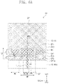
- Each of the plurality of antenna units AN may include a main pattern MA, a plurality of first sub-patterns SA 1 , an antenna line ANL, and an antenna pad ANP.
- the main pattern MA and the plurality of first sub-patterns SA 1 may be disposed in the antenna part AP.
- the antenna pad ANP may be disposed in the peripheral area IS-NAA.
- the antenna line ANL may electrically connect the main pattern MA and the antenna pad ANP.
- the antenna line ANL may be disposed on the display panel DP, and may extend from the main pattern MA disposed in the active area IS-AA to the antenna pad ANP disposed in the peripheral area IS-NAA.
- the main pattern MA and the plurality of first sub-patterns SA 1 may include the same material as some of the plurality of sensing electrodes TE 1 and TE 2 , and may be formed through the same process as some of the plurality of sensing electrodes TE 1 and TE 2 .
- the plurality of first sensing electrodes TE 1 , the main pattern MA, and the plurality of first sub-patterns SA 1 may include carbon nanotubes, metal and/or a metal alloy, or a composite material thereof, and may have a single layer structure or a multilayer structure in which titanium (Ti), aluminum (Al), and titanium (Ti) are sequentially laminated.
- the main pattern MA and the plurality of first sub-patterns SA 1 may include a material different from that of the plurality of first sensing electrodes TE 1 , and may be formed through a process separate from that of the plurality of first sensing electrodes TEE
- the plurality of first sensing electrodes TE 1 may have a multilayer structure in which titanium (Ti), aluminum (Al), and titanium (Ti) are sequentially laminated
- the main pattern MA and the plurality of first sub-patterns SA 1 may include carbon nanotubes, metal and/or a metal alloy, or a composite material thereof, and may have a single layer structure or a multilayer structure.
- the metal material described above may be silver (Ag), copper (Cu), aluminum (Al), gold (Au), or platinum (Pt), and is not limited thereto.
- the antenna line ANL may include the same material as the main pattern MA and the plurality of first sub-patterns SA 1 , and may be formed through the same process as the main pattern MA and the plurality of first sub-patterns SA 1 .
- the antenna line ANL may extend from the main pattern MA toward the peripheral area IS-NAA.
- the antenna pads ANP may be electrically connected to the antenna lines ANL, respectively.
- the plurality of antenna units AN may further include at least one ground electrode disposed below the base insulating layer IS-IL 0 .
- this is exemplary, and the ground electrode according to embodiments of the inventive concept is not limited thereto.
- the ground electrode according to an embodiment of the inventive concept may be the second electrode CE (see FIG. 4 ) of the display panel DP (see FIG. 4 ).
- FIG. 6 A is an enlarged plan view of area AA′ of FIG. 5 A according to an embodiment of the inventive concept.
- some first portions SP 1 a of the plurality of first sensing patterns SP 1 may be patterned in correspondence with shapes of the main pattern MA and the plurality of first sub-patterns SAL
- each of the first portions SP 1 a may be patterned to be spaced apart from the main pattern MA and the plurality of first sub-patterns SA 1 by a predetermined gap.
- the surface area of the sensing part SP (see FIG. 5 A ) for sensing an external input may be increased.
- the sensing part SP is disposed around the antenna part AP (see FIG. 5 A )
- a phenomenon may be prevented in which the main pattern MA and the plurality of first sub-patterns SA 1 are viewed due to differences in reflectance and transmittance, thus improving display quality.
- the main pattern MA and the plurality of first sub-patterns SA 1 may have a mesh structure.
- the plurality of first sub-patterns SA 1 may be spaced apart from one another with the main pattern MA disposed therebetween.
- the first sub-patterns SA 1 may be spaced apart from one another in the second direction DR 2
- the main pattern MA may be disposed between adjacent first sub-patterns SA 1 in the second direction DR 2 , as shown in FIG. 6 A .
- the main pattern MA and the plurality of first sub-patterns SA 1 may overlap the display panel DP (see FIG. 3 ).
- the main pattern MA and the plurality of first sub-patterns SA 1 may be non-overlapping with the light emitting area PXA.
- the main pattern MA and the plurality of first sub-patterns SA 1 overlap the display panel DP and do not overlap the light emitting area PXA.
- the main pattern MA and the plurality of first sub-patterns SA 1 may transmit light emitted from the pixels PX.
- the image IM (see FIG. 1 A ) provided in the active area DP-AA (see FIG. 3 ) may be output to the outside through a plurality of openings OP 0 defined in the main pattern MA and the plurality of first sub-patterns SA 1 .
- each of the plurality of openings OP 0 may overlap the light emitting area PXA.
- the mesh structure may refer to a structure in which a plurality of openings is defined in a predetermined layer.
- the shapes of the main pattern MA and the plurality of first sub-patterns SA 1 may be variously changed in the active area IS-AA according to embodiments.
- the main pattern MA may be designed to operate at a first frequency. Designing the main pattern MA to operate at a frequency may mean designing the main pattern MA to resonate at the first frequency. Thus, in embodiments, the main pattern MA may resonate at the first frequency, and thus, may operate at the first frequency.
- the main pattern MA may transmit and/or receive a signal having the first frequency.
- the main pattern MA may be a patch antenna.
- the first frequency may be about 23 GHz to about 25 GHz, and in an embodiment, may be about 24 GHz. However, this is exemplary, and the first frequency according to embodiments of the inventive concept may be defined as various frequencies according to a signal with which communication is performed.
- the main pattern MA may have a first width LM in the first direction DR 1 .
- the first width LM may be inversely proportional to the first frequency.
- the first width LM may be about 3.9 mm to about 4.3 mm, and in an embodiment, may be about 4.11 mm.
- the main pattern MA may have a second width WM in the second direction DR 2 . Impedance of the main pattern MA may be determined by the second width WM.
- the second width WM may be about 4.8 mm to about 5.1 mm, and in an embodiment, may be about 4.9 mm.
- a plurality of notches NT may be defined in a portion of the main pattern MA where the antenna line ANL is connected to the main pattern MA.
- the impedance of the main pattern MA and impedance of the antenna line ANL may be matched by the plurality of notches NT.
- the impedance of the main pattern MA, the impedance of the antenna line ANL, and the impedance of the plurality of notches NT may be about the same.
- the main pattern MA and the antenna line ANL having the matched impedance may reduce loss of a signal transmitted between the main pattern MA and the antenna line ANL.
- the antenna line ANL may have a width WF in the second direction DR 2 .
- the width WF of the antenna line ANL may be about 0.4 mm to about 0.8 mm, and in an embodiment, may be about 0.58 mm.
- the impedance of the antenna line ANL may be about 45 ⁇ to about 55 ⁇ , and in an embodiment, may be about 50 ⁇ .
- a width LG of each of the plurality of notches NT in the first direction DR 1 may be about 1.0 mm to about 1.4 mm, and in an embodiment, may be about 1.23 mm.
- a width WG of each of the plurality of notches NT in the second direction DR 2 may be about 0.1 mm to about 0.5 mm, and in an embodiment, may be about 0.32 mm.
- the impedance of the main pattern MA and the impedance of the antenna line ANL may be matched by the plurality of notches NT.
- the impedances of the main pattern MA and the antenna line ANL may be matched at about 50 ⁇ . Accordingly, a display device DD (see FIG. 1 A ) may be provided which has an improved signal transmission efficiency between the antenna line ANL and the main pattern MA and an improved communication efficiency.
- the main pattern MA may be a patch antenna.
- the patch antenna may include the main pattern MA having the width WM and the antenna line ANL having the width WF.
- the main pattern MA having the width WM may be referred to as a patch portion of the patch antenna
- the antenna line ANL having the width WF may be referred to as a line portion of the patch antenna.
- a display device DD includes a display panel DP in which an active area DD-AA including a light emitting area PXA and a peripheral area DD-NAA adjacent to the active area DD-AA are defined, and an antenna unit AN disposed on the display panel DP and overlapping the active area DD-AA.
- the antenna unit AN includes a patch antenna (e.g., the main pattern MA) that radiates a first signal at a first frequency in a thickness direction of the patch antenna, and a plurality of first sub-patterns SA 1 that radiates a second signal at a second frequency different from the first frequency in a thickness direction of the plurality of first sub-patterns SA 1 , in which the plurality of first sub-patterns SA 1 is spaced apart from one another with the patch antenna disposed therebetween.
- a patch antenna e.g., the main pattern MA
- a plurality of first sub-patterns SA 1 that radiates a second signal at a second frequency different from the first frequency in a thickness direction of the plurality of first sub-patterns SA 1 , in which the plurality of first sub-patterns SA 1 is spaced apart from one another with the patch antenna disposed therebetween.
- Each of the plurality of first sub-patterns SA 1 may be designed to operate at a second frequency different from the first frequency.
- each of the plurality of first sub-patterns SA 1 may resonate at the second frequency, and thus, may operate at the second frequency.
- Each of the plurality of first sub-patterns SA 1 may transmit and/or receive a signal having the second frequency.
- the second frequency may be higher than the first frequency.
- the second frequency may be a frequency adjacent to the first frequency.
- the second frequency may be about 22 GHz to about 24 GHz, and in an embodiment, may be about 23.5 GHz.
- the second frequency according to embodiments of the inventive concept may be defined as various frequencies according to a signal with which communication is performed.
- Each of the plurality of first sub-patterns SA 1 may have a first width LS in the first direction DR 1 .
- the first width LS may be inversely proportional to the second frequency.
- the first width LS may be determined by the second frequency.
- the first width LM of the main pattern MA may be greater than the first width LS of each of the plurality of first sub-patterns SA 1 .
- the surface area of the main pattern MA may be larger than the surface area of each of the plurality of first sub-patterns SA 1 .
- Each of the plurality of first sub-patterns SA 1 may have a second width WS in the second direction DR 2 .
- the second width WS may determine capacitance between the plurality of first sub-patterns SA 1 and the main pattern MA.
- the capacitance may be inversely proportional to the second width WS.
- Each of the plurality of first sub-patterns SA 1 may be spaced apart from the main pattern MA at a predetermined gap GP in the second direction DR 2 .
- the capacitance may be determined by the gap GP.
- the capacitance may be inversely proportional to the gap GP.
- the plurality of first sub-patterns SA 1 and the main pattern MA may be capacitively coupled by the capacitance.
- the capacitance may change resonance frequencies at which the main pattern MA and the plurality of first sub-patterns SA 1 respectively resonate.
- the plurality of first sub-patterns SA 1 may be spaced apart from one another in the second direction DR 2 with the main pattern MA interposed therebetween.
- the plurality of first sub-patterns SA 1 may be symmetrical in relation to an imaginary line IL extending in the first direction DR 1 .
- the imaginary line IL may overlap the main pattern MA and the antenna line ANL.
- the antenna unit AN may radiate a plurality of wireless communication signals in the third direction DR 3 by the main pattern MA and the plurality of first sub-patterns SA 1 disposed in bilateral symmetry in relation to the imaginary line IL.
- the plurality of wireless communication signals may have certain directionality, and communication efficiency may be improved. Accordingly, the display device DD (see FIG. 1 A ) with improved communication efficiency may be provided.
- FIG. 6 B is an enlarged plan view of area AA′ of FIG. 5 A according to an embodiment of the inventive concept.
- FIG. 6 B is an enlarged plan view of area AA′ of FIG. 5 A according to an embodiment of the inventive concept.
- the input sensor IS may further include a dummy pattern DMP.
- the dummy pattern DMP may be disposed between the plurality of sensing electrodes TE 1 and TE 2 and the main pattern MA.
- the dummy pattern DMP may be disposed between the plurality of sensing electrodes TE 1 and TE 2 and the first sub-patterns SA 1 .
- the dummy pattern DMP may surround the main pattern MA and the plurality of first sub-patterns SA 1 .
- the dummy pattern DMP may have a mesh structure. Utilization of the dummy pattern DMP may reduce a difference between reflectance of an area in which the main pattern MA and the plurality of first sub-patterns SA 1 are disposed and reflectance of an area in which the main pattern MA and the plurality of first sub-patterns SA 1 are not disposed. Accordingly, utilization of the dummy pattern DMP may prevent the main pattern MA and the plurality of first sub-patterns SA 1 from being viewed from the outside.
- the reflectance and transmittance of the area in which the main pattern MA and the plurality of first sub-patterns SA 1 are not disposed may respectively be different from the reflectance and transmittance of the area in which the main pattern MA and the plurality of first sub-patterns SA 1 are disposed.
- the difference between the reflectances and the difference between the transmittances may be reduced by implementing the dummy pattern DMP. As a result, a phenomenon may be prevented in which a particular boundary, for example, a boundary between the main pattern MA and the plurality of first sub-patterns SA 1 and the plurality of sensing patterns SP 2 , is viewed.
- FIG. 7 A is a cross-sectional view taken along line II-II′ of FIG. 6 A according to an embodiment of the inventive concept.
- the main pattern MA and the plurality of first sub-patterns SA 1 may be disposed on the first insulating layer IS-IL 1 .
- the second insulating layer IS-IL 2 may be disposed on the first insulating layer IS-IL 1 .
- the second insulating layer IS-IL 2 may cover the main pattern MA and the plurality of first sub-patterns SA 1 .
- the main pattern MA and the plurality of first sub-patterns SA 1 do not overlap the light emitting area PXA.
- the plurality of second bridge patterns BP 2 may be disposed on the base insulating layer IS-IL 0 .
- the first insulating layer IS-IL 1 may be disposed on the base insulating layer IS-IL 0 .
- the first insulating layer IS-IL 1 may cover the plurality of second bridge patterns BP 2 .
- the plurality of first bridge patterns BP 1 may be disposed on the first insulating layer IS-IL 1 . When viewed in a plane, the plurality of first bridge patterns BP 1 may overlap the plurality of second bridge patterns BP 2 .
- the plurality of first bridge patterns BP 1 may be disposed in the same layer as the main pattern MA and the plurality of first sub-patterns SA 1 .
- the plurality of second bridge patterns BP 2 and the plurality of first bridge patterns BP 1 may be non-overlapping with the light emitting area PXA.
- the plurality of second bridge patterns BP 2 and the plurality of first bridge patterns BP 1 do not overlap the light emitting area PXA.
- the second insulating layer IS-IL 2 may cover the plurality of first bridge patterns BP 1 .
- the plurality of first sensing patterns SP 1 may be disposed on the first insulating layer IS-IL 1 .
- the plurality of first sensing patterns SP 1 may be disposed in the same layer as the plurality of first bridge patterns BP 1 , the main pattern MA, and the plurality of first sub-patterns SA 1 .
- the plurality of first sensing patterns SP 1 , the plurality of first bridge patterns BP 1 , the main pattern MA, and the plurality of first sub-patterns SA 1 may be formed by the same process. However, this is exemplary, and the process of forming these elements according to embodiments of the inventive concept is not limited thereto.
- the plurality of first sensing patterns SP 1 may be formed through the same process as the plurality of first bridge patterns BP 1 , and the main pattern MA may be formed by the same process as the plurality of first sub-patterns SA 1 .
- the plurality of first sensing patterns SP 1 may be non-overlapping with the light emitting area PXA.
- the plurality of first sensing patterns SP 1 does not overlap the light emitting area PXA.
- the second insulating layer IS-IL 2 may cover the plurality of first sensing patterns SP 1 .
- FIG. 7 B is a cross-sectional view taken along line II-II′ of FIG. 6 A according to an embodiment of the inventive concept.
- FIG. 7 B is a cross-sectional view taken along line II-II′ of FIG. 6 A according to an embodiment of the inventive concept.
- a main pattern MAa and a plurality of first sub-patterns SA 1 a may be disposed on the base insulating layer IS-IL 0 .
- the first insulating layer IS-IL 1 may cover the main pattern MAa and the plurality of first sub-patterns SA 1 a .
- the main pattern MAa and the plurality of first sub-patterns SA 1 a may be non-overlapping with the light emitting area PXA.
- the main pattern MAa and the plurality of first sub-patterns SA 1 a do not overlap the light emitting area PXA.
- the main pattern MAa and the plurality of first sub-patterns SA 1 a may be disposed in the same layer as the plurality of second bridge patterns BP 2 .
- the main pattern MAa, the plurality of first sub-patterns SA 1 a , and the plurality of second bridge patterns BP 2 may be formed by the same process.
- this is exemplary, and the process of forming the main pattern MAa, the plurality of first sub-patterns SA 1 a , and the plurality of second bridge patterns BP 2 according to embodiments of the inventive concept is not limited thereto.
- the main pattern MAa may be formed by the same process as the plurality of first sub-patterns SA 1 a
- the plurality of second bridge patterns BP 2 may be formed by the same process.
- FIGS. 8 A and 8 B are graphs showing an S-parameter, according to frequency, of an antenna unit according to embodiments of the inventive concept.
- S 11 may be one of S-parameters.
- S 11 may be a value representing a ratio of the strength of a reflected signal generated from the reflection of an input signal to the strength of the input signal.
- S 11 may be a reflection coefficient of the antenna unit AN (see FIG. 5 A ).
- the operation of the antenna unit AN may be determined on the basis of a case that S 11 is about ⁇ 10 dB.
- the value of about ⁇ 10 dB may refer to a case in which the strength of a reflected signal generated from the reflection of an input signal is about 10% of the strength of the input signal.
- the antenna unit AN may be determined as operating in a corresponding frequency band.
- the S-parameter of the antenna unit AN in which the predetermined gap GP between the main pattern MA and the plurality of first sub-patterns SA 1 is a first gap may have the shape of a first graph G 11 shown in FIG. 8 A .
- the S-parameter of the antenna unit AN in which the predetermined gap GP between the main pattern MA and the plurality of first sub-patterns SA 1 is a second gap different from the first gap may have the shape of a second graph G 12 as shown in FIG. 8 B .
- the first gap may be greater than the second gap.
- the main pattern MA and the plurality of first sub-patterns SA 1 may be capacitively coupled. Due to an electromagnetic interaction of the capacitive coupling, resonance frequencies of the main pattern MA and each of the plurality of first sub-patterns SA 1 may vary depending on the predetermined gap GP and the second width WS of each of the plurality of first sub-patterns SAL 1 .
- the main pattern MA may radiate a first signal.
- the first signal may have a first frequency band.
- the plurality of first sub-patterns SA 1 may radiate a second signal.
- the second signal may have a second frequency band. A portion of the first frequency band and a portion of the second frequency band may overlap.
- the antenna unit AN (see FIG. 5 A ) may operate in a frequency band BW.
- the frequency band BW in which the antenna unit AN (see FIG. 5 A ) operates may be wideband. Accordingly, the display device DD (see FIG. 1 A ) with an improved frequency bandwidth may be provided.
- the main pattern MA may radiate a third signal.
- the third signal may have a third frequency band BW 1 .
- the plurality of first sub-patterns SA 1 may radiate a fourth signal.
- the fourth signal may have a fourth frequency band BW 2 .
- the third frequency band BW 1 and the fourth frequency band BW 2 may be different from each other.
- the antenna unit AN (see FIG. 5 A ) may operate in the plurality of frequency bands BW 1 and BW 2 .
- the antenna unit AN may operate in the plurality of frequency bands different from one another.
- the antenna unit AN may operate in multiple frequency bands. Accordingly, the display device DD (see FIG. 1 A ) with an improved frequency bandwidth may be provided.
- FIG. 9 A illustrates a radiation pattern in a magnetic field of an antenna unit according to an embodiment of the inventive concept.
- FIG. 9 B illustrates a radiation pattern in an electric field of an antenna unit according to an embodiment of the inventive concept.
- FIGS. 9 A and 9 B illustrate radiation patterns of the first graph G 11 .
- an antenna gain is about 0 dB or larger in a radiation pattern
- a signal is radiated in a corresponding direction.
- a direction indicated by 0° may be the third direction DR 3 .
- FIG. 9 A illustrates a radiation pattern of a cross section, taken along the second direction DR 2 , of the antenna unit AN (see FIG. 5 A ).
- a direction indicated by 90° may be the second direction DR 2 .
- FIG. 9 B illustrates a radiation pattern of a cross section, taken along the first direction DR 1 , of the antenna unit AN (see FIG. 5 A ).
- a direction indicated by 90° may be the first direction DR 1 .
- the main pattern MA may radiate a first signal GG 11 .
- the first signal GG 11 may have the first frequency band.
- the plurality of first sub-patterns SA 1 may radiate a second signal GG 12 .
- the second signal GG 12 may have the second frequency band.
- a portion, in a radiation pattern of the first signal GG 11 may indicate a thickness direction of the main pattern MA.
- the first signal GG 11 may be radiated from the main pattern MA in the thickness direction of the main pattern MA.
- a portion, in a radiation pattern of the second signal GG 12 may indicate a thickness direction of each of the plurality of first sub-patterns SA 1 .
- the second signal GG 12 may be radiated from each of the plurality of first sub-patterns SA 1 in the thickness direction of each of the plurality of first sub-patterns SAL
- the thickness direction may be the third direction DR 3 .
- the first signal GG 11 and the second signal GG 12 may have an antenna gain of about 0 dB or larger in the range of about 330° to about 30° in the radiation patterns. In this case, the first signal GG 11 and the second signal GG 12 have directionality in the third direction DR 3 .
- the antenna unit AN may radiate a signal in the third direction DR 3 .
- the signal may have directionality.
- the antenna unit AN may improve the concentration of antenna gain.
- the display device DD see FIG. 1 A ) may be provided which has an improved transmission distance for the signal transmitted and/or received via the antenna unit AN.
- the shapes of the radiation patterns of the first signal GG 11 and the second signal GG 12 may be similar.
- the antenna unit AN (see FIG. 5 A ) may operate in a wide band.
- the frequency band BW in which the antenna unit AN (see FIG. 5 A ) operates may be wideband. Accordingly, the display device DD (see FIG. 1 A ) with an improved frequency bandwidth may be provided.
- a portion, in a radiation pattern of the first signal GG 11 may indicate the thickness direction of the main pattern MA.
- the first signal GG 11 may be radiated from the main pattern MA in the thickness direction of the main pattern MA.
- a portion, in a radiation pattern of the second signal GG 12 may indicate the thickness direction of each of the plurality of first sub-patterns SA 1 .
- the second signal GG 12 may be radiated from each of the plurality of first sub-patterns SA 1 in the thickness direction of each of the plurality of first sub-patterns SA 1 .
- the antenna unit AN may radiate a signal in the third direction DR 3 .
- the signal may have directionality.
- the antenna unit AN (see FIG. 5 A ) may improve the concentration of antenna gain.
- the display device DD (see FIG. 1 A ) may be provided which has an improved transmission distance for the signal transmitted and/or received via the antenna unit AN.
- FIG. 10 A is a plan view illustrating an antenna unit according to an embodiment of the inventive concept.
- an antenna unit AN 1 may have a mesh structure.
- a plurality of openings OP 1 may be defined in the antenna unit AN 1 .
- the antenna unit AN 1 may include a main pattern MA 1 , a plurality of first sub-patterns SA 11 , and a plurality of second sub-patterns SA 21 .
- the main pattern MA 1 , the plurality of first sub-patterns SA 11 , and the plurality of second sub-patterns SA 21 may be spaced apart from one another in the second direction DR 2 .
- the plurality of first sub-patterns SA 11 may be disposed between the plurality of second sub-patterns SA 21 and the main pattern MA 1 in the second direction DR 2 .
- one of the second sub-patterns SA 21 may be spaced apart from the main pattern MA 1 with one of the first sub-patterns SA 11 disposed therebetween, as shown in FIG. 10 A .
- the plurality of second sub-patterns SA 21 may be capacitively coupled to the plurality of first sub-patterns SA 11 .
- the main pattern MA 1 may be designed to operate at a first frequency.
- the main pattern MA 1 may resonate at the first frequency, and thus, may operate at the first frequency.
- the main pattern MA 1 may transmit and/or receive a signal having the first frequency.
- the main pattern MA 1 may be a patch antenna.
- the first frequency may be about 38 GHz to about 40 GHz, and in an embodiment, may be about 39 GHz.
- this is exemplary, and the first frequency according to embodiments of the inventive concept may be defined as various frequencies according to a signal with which communication is performed.
- the main pattern MA 1 may have a first width LMa in the first direction DR 1 .
- the first width LMa may be inversely proportional to the first frequency.
- the first width LMa may be about 2.4 mm to about 2.8 mm, and in an embodiment, may be about 2.58 mm.
- the main pattern MA 1 may have a second width WMa in the second direction DR 2 . Impedance of the main pattern MA 1 may be determined by the second width WMa.
- the second width WMa may be about 1.8 mm to about 2.2 mm, and in an embodiment, may be about 2.0 mm.
- a plurality of notches NT 1 may be defined in a portion of the main pattern MA 1 where the antenna line ANL is connected to the main pattern MA 1 .
- the impedance of the main pattern MA 1 and the impedance of the antenna line ANL may be matched by the plurality of notches NT 1 .
- the impedance of the main pattern MA 1 , the impedance of the antenna line ANL, and the impedance of the plurality of notches NT 1 may be about the same.
- the main pattern MA 1 and the antenna line ANL having the matched impedance may reduce loss of a signal transmitted to each other.
- the impedance of the antenna line ANL may be about 4 ⁇ to about 55 ⁇ , and in an embodiment, may be about 50 ⁇ .
- a width LGa of each of the plurality of notches NT 1 in the first direction DR 1 may be about 0.8 mm to about 1.2 mm, and in an embodiment, may be about 0.98 mm.
- a width WGa of each of the plurality of notches NT 1 in the second direction DR 2 may be about 0.01 mm to about 0.4 mm, and in an embodiment, may be about 0.2 mm.
- the impedance of the main pattern MA 1 and the impedance of the antenna line ANL may be matched by the plurality of notches NT 1 .
- the impedance of the main pattern MA 1 , the impedance of the antenna line ANL, and the impedance of the plurality of notches NT 1 may be about the same.
- the impedances of the main pattern MA 1 and the antenna line ANL may be matched at about 50 ⁇ . Accordingly, the display device DD (see FIG. 1 A ) may be provided which has an improved signal transmission efficiency between the antenna line ANL and the main pattern MA 1 and an improved communication efficiency.
- Each of the plurality of first sub-patterns SA 11 may be designed to operate at a second frequency different from the first frequency.
- each of the plurality of first sub-patterns SA 11 may resonate at the second frequency, and thus, may operate at the second frequency.
- Each of the plurality of first sub-patterns SA 11 may transmit and/or receive a signal having the second frequency.
- the second frequency may be lower than the first frequency.
- the second frequency may be about 26 GHz to about 28 GHz, and in an embodiment, may be about 27.7 GHz.
- the second frequency according to embodiments of the inventive concept may be defined as various frequencies according to a signal with which communication is performed.
- Each of the plurality of first sub-patterns SA 11 may have a first width LSa in the first direction DR 1 .
- the first width LSa may be inversely proportional to the second frequency.
- the first width LSa may be determined by the second frequency.
- the first width LMa of the main pattern MA 1 may be smaller than the first width LSa of each of the plurality of first sub-patterns SA 11 .
- Each of the plurality of first sub-patterns SA 11 may have a second width WSa in the second direction DR 2 .
- the second width WSa of the plurality of first sub-patterns SA 11 may be smaller than the second width WMa of the main pattern MA 1 .
- Each of the plurality of first sub-patterns SA 11 may be spaced apart from the main pattern MA 1 at a predetermined first gap GP 1 in the second direction DR 2 .
- the first gap GP 1 may be about 0.005 mm to about 0.015 mm, and in an embodiment, may be about 0.01 mm.
- the plurality of first sub-patterns SA 11 may be spaced apart from one another in the second direction DR 2 with the main pattern MA 1 interposed therebetween.
- Each of the plurality of second sub-patterns SA 21 may operate at a third frequency different from the first frequency and the second frequency.
- each of the plurality of second sub-patterns SA 21 may resonate at the third frequency, and thus, may operate at the third frequency.
- Each of the plurality of second sub-patterns SA 21 may transmit and/or receive a signal having the third frequency.
- the third frequency may be lower than the first frequency and the second frequency.
- the third frequency may be about 22 GHz to about 24 GHz, and in an embodiment, may be about 23.6 GHz.
- the third frequency according to embodiments of the inventive concept may be defined as various frequencies according to a signal with which communication is performed.
- the first frequency is higher than the second frequency
- the second frequency is higher than the third frequency.
- Each of the plurality of second sub-patterns SA 21 may have a first width LSb in the first direction DR 1 .
- the first width LSb may be inversely proportional to the third frequency.
- the first width LSb may be determined by the third frequency.
- the first width LMa of the main pattern MA 1 and the first width LSa of each of the plurality of first sub-patterns SA 11 may be smaller than the first width LSb of each of the plurality of second sub-patterns SA 21 .
- the first width LMa of the main pattern MA 1 is smaller than the first width LSa of each of the plurality of first sub-patterns SA 11
- the first width LSa of each of the plurality of first sub-patterns SA 11 is smaller than the first width LSb of each of the plurality of second sub-patterns SA 21 .
- Each of the plurality of second sub-patterns SA 21 may have a second width WSb in the second direction DR 2 .
- the second width WSb of the plurality of second sub-patterns SA 21 may be smaller than the second width WMa of the main pattern MA 1 .
- the plurality of second sub-patterns SA 21 may respectively be spaced apart from the plurality of first sub-patterns SA 11 at a predetermined second gap GP 2 in the second direction DR 2 .
- the second gap GP 2 may be about 0.005 mm to about 0.015 mm, and in an embodiment, may be about 0.01 mm.
- the plurality of second sub-patterns SA 21 may be spaced apart from the main pattern MA 1 with the plurality of first sub-patterns SA 11 , respectively, interposed therebetween.
- the plurality of second sub-patterns SA 21 may be spaced apart from one another in the second direction DR 2 with the main pattern MA 1 interposed therebetween.
- the plurality of first sub-patterns SA 1 is spaced apart from one another with the main pattern MA 1 disposed therebetween, and the plurality of second sub-patterns SA 21 is spaced apart from one another with the main pattern MA 1 disposed therebetween.
- adjacent first sub-patterns SA 11 may be spaced apart from one another with the main pattern MA 1 disposed therebetween, and adjacent second sub-patterns SA 21 may be spaced apart from one another with the main pattern MA 1 disposed therebetween.
- the plurality of first sub-patterns SA 11 may be symmetrical in relation to an imaginary line IL 1 extending in the first direction DR 1 .
- the plurality of second sub-patterns SA 21 may be symmetrical in relation to the imaginary line IL 1 .
- the imaginary line IL 1 may extend along and overlap the main pattern MA 1 and the antenna line ANL.
- the antenna unit AN 1 may radiate a plurality of wireless communication signals in the third direction DR 3 by the main pattern MA 1 , the plurality of first sub-patterns SA 11 , and the plurality of second sub-patterns SA 21 disposed in bilateral symmetry in relation to the imaginary line IL 1 .
- the plurality of wireless communication signals may have certain directionality, and communication efficiency may be improved. Accordingly, the display device DD (see FIG. 1 A ) with improved communication efficiency may be provided.
- the main pattern MA 1 and the plurality of first sub-patterns SA 11 may be capacitively coupled.
- the main pattern MA 1 and the plurality of second sub-patterns SA 21 may be capacitively coupled.
- the plurality of first sub-patterns SA 1 may be capacitively coupled to the plurality of second sub-patterns SA 21 , respectively.
- resonance frequencies may change at which the main pattern MA 1 , the plurality of first sub-patterns SA 11 , and the plurality of second sub-patterns SA 21 respectively resonate.
- FIG. 10 B is a plan view illustrating an antenna unit according to an embodiment of the inventive concept.
- FIG. 10 B is a plan view illustrating an antenna unit according to an embodiment of the inventive concept.
- an antenna unit AN 2 may include the main pattern MA, the plurality of first sub-patterns SA 1 , and a sub-pattern SA 0 .
- the sub-pattern SA 0 may be spaced apart from the main pattern MA in the first direction DR 1 .
- the sub-pattern SA 0 and the main pattern MA may be capacitively coupled. Due to an electromagnetic interaction of the capacitive coupling of the main pattern MA, the plurality of first sub-patterns SA 1 , and the sub-pattern SA 0 , resonance frequencies may change at which the main pattern MA, the plurality of first sub-patterns SA 1 , and the sub-pattern SA 0 respectively resonate.
- a frequency band BW in which the antenna unit AN 2 operates may be wideband or multiband depending on the resonance frequency at which the sub-pattern SA 0 resonates. Accordingly, the display device DD (see FIG. 1 A ) with an improved frequency bandwidth may be provided.
- FIG. 11 is a cross-sectional view taken along line III-III′ of FIG. 10 A according to an embodiment of the inventive concept.
- the main pattern MA 1 , the plurality of first sub-patterns SA 11 , and the plurality of second sub-patterns SA 21 may be disposed on the first insulating layer IS-IL 1 .
- the second insulating layer IS-IL 2 may cover the main pattern MA 1 , the plurality of first sub-patterns SA 11 , and the plurality of second sub-patterns SA 21 .
- this is exemplary, and the arrangement of the main pattern MA 1 , the plurality of first sub-patterns SA 11 , and the plurality of second sub-patterns SA 21 according to embodiments of the inventive concept is not limited thereto.
- the main pattern MA 1 , the plurality of first sub-patterns SA 11 , and the plurality of second sub-patterns SA 21 may be disposed on the base insulating layer IS-IL 0 , and the first insulating layer IS-IL 1 may cover the main pattern MA 1 , the plurality of first sub-patterns SA 11 , and the plurality of second sub-patterns SA 21 .
- the plurality of openings OP 1 may overlap the light emitting area PXA.
- the main pattern MA 1 , the plurality of first sub-patterns SA 11 , and the plurality of second sub-patterns SA 21 may be non-overlapping with the light emitting area PXA.
- the main pattern MA 1 , the plurality of first sub-patterns SA 11 , and the plurality of second sub-patterns SA 21 do not overlap the light emitting area PXA.
- FIG. 12 is a graph showing an S-parameter, according to frequency, of an antenna unit according to an embodiment of the inventive concept.
- the S-parameter of the antenna unit AN 1 may have a shape of a third graph G 21 .
- the main pattern MA 1 , the plurality of first sub-patterns SA 11 , and the plurality of second sub-patterns SA 21 may be capacitively coupled to one another.
- the main pattern MA 1 may radiate a first signal.
- the first signal may have a first frequency band FQ 21 .
- the plurality of first sub-patterns SA 11 may radiate a second signal.
- the second signal may have a second frequency band FQ 22 .
- the plurality of second sub-patterns SA 21 may radiate a third signal.
- the third signal may have a third frequency band FQ 23 .
- the first frequency band FQ 21 , the second frequency band FQ 22 , and the third frequency band FQ 23 may be different from one another.
- the antenna unit AN 1 may operate in the plurality of frequency bands FQ 21 , FQ 22 , and FQ 23 .
- the antenna unit AN 1 may operate in the plurality of frequency bands different from one another.
- the antenna unit AN 1 may operate in multiple frequency bands. Accordingly, the display device DD (see FIG. 1 A ) with an improved frequency bandwidth may be provided.
- FIG. 13 A illustrates a radiation pattern in a magnetic field of an antenna unit according to an embodiment of the inventive concept.
- FIG. 13 B illustrates a radiation pattern in an electric field of an antenna unit according to an embodiment of the inventive concept.
- FIGS. 13 A and 13 B illustrate radiation patterns of the third graph G 21 .
- the main pattern MA 1 may radiate a first signal GG 31 .
- the first signal GG 31 may have the first frequency band.
- the plurality of first sub-patterns SA 11 may radiate a second signal GG 32 .
- the second signal GG 32 may have the second frequency band.
- the plurality of second sub-patterns SA 21 may radiate a third signal GG 33 .
- the third signal GG 33 may have the third frequency band.
- the first signal GG 31 may be radiated from the main pattern MA 1 in the thickness direction of the main pattern MA 1 .
- a portion, in a radiation pattern of the second signal GG 32 whose value is about 0 dB or larger, may indicate a thickness direction of each of the plurality of first sub-patterns SA 11 .
- the second signal GG 32 may be radiated from each of the plurality of first sub-patterns SA 11 in the thickness direction of each of the plurality of first sub-patterns SA 11 .
- a portion, in a radiation pattern of the third signal GG 33 may indicate a thickness direction of each of the plurality of second sub-patterns SA 21 .
- the third signal GG 33 may be radiated from each of the plurality of second sub-patterns SA 21 in the thickness direction of each of the plurality of second sub-patterns SA 21 .
- the thickness direction may be the third direction DR 3 .
- the first signal GG 31 , the second signal GG 32 , and the third signal GG 33 may have an antenna gain of about 0 dB or larger in the range of about 330° to about 30° in the radiation patterns.
- the first signal GG 31 , the second signal GG 32 , and the third signal GG 33 have directionality in the third direction DR 3 .
- the antenna unit AN 1 may radiate a signal in the third direction DR 3 .
- the signal may have directionality.
- the antenna unit AN 1 may improve the concentration of antenna gain.
- the display device DD see FIG. 1 A ) may be provided which has an improved transmission distance for the signal transmitted and/or received via the antenna unit AN 1 .
- the shapes of the radiation patterns of the first signal GG 31 , the second signal GG 32 , and the third signal GG 33 may be different.
- a multiband operation of the antenna unit AN 1 may be provided.
- the frequency bands FQ 21 , FQ 22 , and FQ 23 in which the antenna unit AN 1 operates may be multiband. Accordingly, the display device DD (see FIG. 1 A ) with an improved frequency bandwidth may be provided.
- FIG. 14 is an enlarged plan view of area AA′ of FIG. 5 A according to an embodiment of the inventive concept. For convenience of explanation, a further description of elements and technical aspects previously described may be omitted herein.
- an antenna unit AN 3 may include a main pattern MA 3 , a plurality of first sub-patterns SA 13 , and the antenna line ANL 3 . Although one antenna unit AN 3 is illustrated in FIG. 14 , the antenna unit AN 3 may be provided in plurality in embodiments.
- the antenna unit AN 3 may be disposed on a first sensing pattern SP 1 of the first sensing patterns SP 1 and a plurality of second sensing patterns SP 2 adjacent thereto.
- the illustration of FIG. 14 is exemplary, and a component overlapping the antenna unit AN 3 may be changed according to the size and position of the antenna unit AN 3 according to embodiments.
- the antenna unit AN 3 may be disposed only on the first sensing pattern SP 1 .
- the display device DD may sense an external input even in an area in which the antenna unit AN 3 is disposed. Accordingly, in embodiments, even when the antenna unit AN 3 is disposed, the surface area of the sensing part SP (see FIG. 1 A ) of the input sensor IS (see FIG. 1 A ) is not reduced.
- FIG. 15 is a cross-sectional view of a display device according to an embodiment of the inventive concept.
- a display device DDb may include a display panel DPb, an input sensor ISb, an antenna layer PP, and a window WPb.
- the input sensor ISb may be disposed on the display panel DPb.
- the input sensor ISb may sense an external input applied from the outside.
- the external input may be a user input.
- the user input may include various types of external inputs such as, for example, a part of a user's body, light, heat, pen, and pressure.
- the antenna layer PP may be disposed on the input sensor ISb.
- the antenna layer PP may be formed on the input sensor ISb through a continuous process.
- the antenna layer PP may be bonded to the input sensor ISb by an adhesive member.
- the adhesive member may include a typical adhesive or a typical detachable adhesive.
- the adhesive member may be a transparent adhesive member such as a Pressure Sensitive Adhesive (PSA) film, an Optically Clear Adhesive (OCA) film, or an Optically Clear Resin (OCR).
- PSA Pressure Sensitive Adhesive
- OCA Optically Clear Adhesive
- OCR Optically Clear Resin
- the antenna layer PP may be disposed between the input sensor ISb and the window WPb.
- FIG. 16 is a cross-sectional view taken along line IV-IV′ of FIG. 14 according to an embodiment of the inventive concept.
- the first sensing pattern SP 1 may be disposed on the first insulating layer IS-IL 1 .
- the second insulating layer IS-IL 2 may cover the first sensing pattern SP 1 .
- the antenna layer PP may be disposed on an input sensor ISc.
- the main pattern MA 3 and each of the first sub-patterns SA 13 may be disposed on the second insulating layer IS-IL 2 . When viewed in a plane, each of the main pattern MA 3 and the first sub-pattern SA 13 may overlap the first sensing pattern SP 1 . When viewed in a plane, the first sensing pattern SP 1 , the main pattern MA 3 , and the first sub-pattern SA 13 may be non-overlapping with the light emitting area PXA.
- each of the main pattern MA 3 and the first sub-pattern SA 13 overlaps the first sensing pattern SP 1 , and the first sensing pattern SP 1 , the main pattern MA 3 , and the first sub-pattern SA 13 do not overlap the light emitting area PXA.
- the first sensing pattern SP 1 may be disposed below the main pattern MA 3 and the first sub-pattern SA 13 . Because the main pattern MA 3 and the first sub-pattern SA 13 overlap the first portion SP 1 , the display device DD (see FIG. 1 A ) may sense an external input even in an area in which the main pattern MA 3 and the first sub-pattern SA 13 are disposed. Accordingly, in an embodiment, the surface area of the sensing part of the input sensor ISc is not reduced.
- FIG. 17 is a cross-sectional view taken along line IV-IV′ of FIG. 14 according to an embodiment of the inventive concept.
- an input sensor ISd may include the base insulating layer IS-IL 0 , the first insulating layer IS-IL 1 , the second insulating layer IS-IL 2 , the first sensing pattern SP 1 , the main pattern MA 3 , and the first sub-pattern SA 13 .
- the input sensor ISd may be a top bridge structure in which the plurality of second bridge patterns BP 2 (see FIG. 5 A ) is disposed on the plurality of first bridge patterns BP 1 (see FIG. 5 A ).
- the first sensing pattern SP 1 is part of the first sensing electrode TEE
- the first sensing pattern SP 1 may be disposed on the base insulating layer IS-IL 0 .
- the first insulating layer IS-IL 1 may cover the first sensing pattern SP 1 .
- the main pattern MA 3 and the first sub-pattern SA 13 may be disposed on the first insulating layer IS-ILE
- the second insulating layer IS-IL 2 may cover the main pattern MA 3 and the first sub-pattern SA 13 .
- each of the main pattern MA 3 and the first sub-pattern SA 13 may overlap the first sensing pattern SP 1 .
- the first sensing pattern SP 1 , the main pattern MA 3 , and the first sub-pattern SA 13 may be non-overlapping with the light emitting area PXA.
- each of the main pattern MA 3 and the first sub-pattern SA 13 overlaps the first sensing pattern SP 1 , and the first sensing pattern SP 1 , the main pattern MA 3 , and the first sub-pattern SA 13 do not overlap the light emitting area PXA.
- each of the main pattern MA 3 and the first sub-pattern SA 13 may overlap the first sensing pattern SP 1 even in the form in which the antenna unit AN 3 (see FIG. 14 ) is embedded in the input sensor ISd.
- the display device DD may sense an external input. Accordingly, in an embodiment, the surface area of the sensing part of the input sensor ISd is not reduced.
- the antenna unit may radiate a plurality of wireless communication signals in the thickness direction by the main pattern and the plurality of first sub-patterns disposed in bilateral symmetry.
- the plurality of wireless communication signals may have certain directionality.
- the antenna unit may improve the concentration of antenna gain. Accordingly, embodiments may provide a display device having improved communication efficiency and signal transmission distance.
- the frequency band in which the antenna unit operates may be a wide band, or may be multiple frequency bands including a plurality of frequency bands different from one another. Accordingly, a display device with improved frequency bandwidth may be provided.
Landscapes
- Engineering & Computer Science (AREA)
- Physics & Mathematics (AREA)
- Theoretical Computer Science (AREA)
- General Engineering & Computer Science (AREA)
- General Physics & Mathematics (AREA)
- Human Computer Interaction (AREA)
- Computer Networks & Wireless Communication (AREA)
- Nonlinear Science (AREA)
- Microelectronics & Electronic Packaging (AREA)
- Mathematical Physics (AREA)
- Optics & Photonics (AREA)
- Chemical & Material Sciences (AREA)
- Crystallography & Structural Chemistry (AREA)
- Electromagnetism (AREA)
- Devices For Indicating Variable Information By Combining Individual Elements (AREA)
- Electroluminescent Light Sources (AREA)
- Vehicle Body Suspensions (AREA)
- Diaphragms For Electromechanical Transducers (AREA)
- Measuring Pulse, Heart Rate, Blood Pressure Or Blood Flow (AREA)
Abstract
Description
Claims (28)
Applications Claiming Priority (2)
| Application Number | Priority Date | Filing Date | Title |
|---|---|---|---|
| KR1020200040559A KR102862597B1 (en) | 2020-04-02 | 2020-04-02 | Display device |
| KR10-2020-0040559 | 2020-04-02 |
Publications (2)
| Publication Number | Publication Date |
|---|---|
| US20210313691A1 US20210313691A1 (en) | 2021-10-07 |
| US11527826B2 true US11527826B2 (en) | 2022-12-13 |
Family
ID=74859233
Family Applications (1)
| Application Number | Title | Priority Date | Filing Date |
|---|---|---|---|
| US17/123,614 Active 2041-02-04 US11527826B2 (en) | 2020-04-02 | 2020-12-16 | Display device |
Country Status (4)
| Country | Link |
|---|---|
| US (1) | US11527826B2 (en) |
| EP (1) | EP3890108A1 (en) |
| KR (1) | KR102862597B1 (en) |
| CN (1) | CN113517552A (en) |
Families Citing this family (3)
| Publication number | Priority date | Publication date | Assignee | Title |
|---|---|---|---|---|
| KR102781236B1 (en) * | 2020-06-11 | 2025-03-12 | 동우 화인켐 주식회사 | Antenna device and display device including the same |
| KR102776232B1 (en) * | 2020-08-31 | 2025-03-07 | 삼성디스플레이 주식회사 | Radio frequency device and electronic device having the same |
| CN117135951A (en) | 2022-05-17 | 2023-11-28 | 群创光电股份有限公司 | display device |
Citations (13)
| Publication number | Priority date | Publication date | Assignee | Title |
|---|---|---|---|---|
| US20080316110A1 (en) | 2007-06-22 | 2008-12-25 | Suncall Corporation | Patch Antenna and RFID Inlet |
| US20130169503A1 (en) | 2011-12-30 | 2013-07-04 | Mohammad Fakharzadeh Jahromi | Parasitic patch antenna |
| US20140106684A1 (en) * | 2012-10-15 | 2014-04-17 | Qualcomm Mems Technologies, Inc. | Transparent antennas on a display device |
| KR20140100822A (en) * | 2013-02-07 | 2014-08-18 | 삼성디스플레이 주식회사 | Touch Screen Panel Having Antenna Pattern and Display Device Having the Same |
| KR20140120520A (en) | 2013-04-03 | 2014-10-14 | 엘지전자 주식회사 | Mobile terminal |
| US20150255856A1 (en) | 2014-03-05 | 2015-09-10 | Samsung Electronics Co., Ltd. | Antenna device and electronic device having the antenna device |
| US20160093939A1 (en) * | 2014-09-25 | 2016-03-31 | Samsung Electronics Co., Ltd. | Antenna Device |
| US20160126614A1 (en) * | 2014-10-29 | 2016-05-05 | Samsung Electronics Co., Ltd. | Antenna Device and Electronic Device Having the Same |
| US20160315397A1 (en) | 2015-04-21 | 2016-10-27 | Kyocera Corporation | Antenna board |
| US20190058264A1 (en) * | 2017-08-17 | 2019-02-21 | Lg Electronics Inc. | Electronic device |
| KR20190019802A (en) | 2017-08-17 | 2019-02-27 | 엘지전자 주식회사 | Electronic device |
| KR101962820B1 (en) | 2017-11-06 | 2019-03-27 | 동우 화인켐 주식회사 | Film antenna and display device including the same |
| KR20190069226A (en) | 2017-12-11 | 2019-06-19 | 엘지디스플레이 주식회사 | Organic light emitting display panel with antenna and electronic device with the same |
Family Cites Families (1)
| Publication number | Priority date | Publication date | Assignee | Title |
|---|---|---|---|---|
| KR102406686B1 (en) * | 2015-11-10 | 2022-06-08 | 삼성전자주식회사 | Antenna device and electronic device with the same |
-
2020
- 2020-04-02 KR KR1020200040559A patent/KR102862597B1/en active Active
- 2020-12-16 US US17/123,614 patent/US11527826B2/en active Active
-
2021
- 2021-03-05 EP EP21160848.4A patent/EP3890108A1/en active Pending
- 2021-03-23 CN CN202110308267.7A patent/CN113517552A/en active Pending
Patent Citations (14)
| Publication number | Priority date | Publication date | Assignee | Title |
|---|---|---|---|---|
| US20080316110A1 (en) | 2007-06-22 | 2008-12-25 | Suncall Corporation | Patch Antenna and RFID Inlet |
| US20130169503A1 (en) | 2011-12-30 | 2013-07-04 | Mohammad Fakharzadeh Jahromi | Parasitic patch antenna |
| US20140106684A1 (en) * | 2012-10-15 | 2014-04-17 | Qualcomm Mems Technologies, Inc. | Transparent antennas on a display device |
| KR20140100822A (en) * | 2013-02-07 | 2014-08-18 | 삼성디스플레이 주식회사 | Touch Screen Panel Having Antenna Pattern and Display Device Having the Same |
| KR20140120520A (en) | 2013-04-03 | 2014-10-14 | 엘지전자 주식회사 | Mobile terminal |
| US20150255856A1 (en) | 2014-03-05 | 2015-09-10 | Samsung Electronics Co., Ltd. | Antenna device and electronic device having the antenna device |
| US20160093939A1 (en) * | 2014-09-25 | 2016-03-31 | Samsung Electronics Co., Ltd. | Antenna Device |
| US20160126614A1 (en) * | 2014-10-29 | 2016-05-05 | Samsung Electronics Co., Ltd. | Antenna Device and Electronic Device Having the Same |
| US20160315397A1 (en) | 2015-04-21 | 2016-10-27 | Kyocera Corporation | Antenna board |
| US20190058264A1 (en) * | 2017-08-17 | 2019-02-21 | Lg Electronics Inc. | Electronic device |
| KR20190019802A (en) | 2017-08-17 | 2019-02-27 | 엘지전자 주식회사 | Electronic device |
| US10381750B2 (en) | 2017-08-17 | 2019-08-13 | Lg Electronics Inc. | Electronic device |
| KR101962820B1 (en) | 2017-11-06 | 2019-03-27 | 동우 화인켐 주식회사 | Film antenna and display device including the same |
| KR20190069226A (en) | 2017-12-11 | 2019-06-19 | 엘지디스플레이 주식회사 | Organic light emitting display panel with antenna and electronic device with the same |
Non-Patent Citations (8)
| Title |
|---|
| European Extended Search Report dated Aug. 31, 2021 from the European Patent Office corresponding to European Patent Appln. No. 21160848.4. |
| J. A. Ansari et al., Analysis of Multilayer Rectangular Patch Antenna for Broadband Operation, Wireless Pers Commun (2012) 62:315-327. |
| Lee et al., Machine Translation of Foreign Patent Document KR 20140100822A, Touch screen panel having antenna pattern and display device having the same, Aug. 18, 2014, pp. 1-17 (Year: 2014). * |
| Mekala Harinath Reddy et al., Bandwidth Enhancement of Microstrip Patch Antenna using Parasitic Patch, 017 IEEE International Conference on Smart Technologies and Management for Computing, Communication, Controls, Energy and Materials (ICSTM), Veltech Dr.RR & Dr.SR University, Chennai, T.N., India. Aug. 2-4, 2017. pp. 295-298. |
| Syamimi Mohd Norzeli et al., Design of High Gain Microstrip Patch Reader Array Antenna with Parasitic Elements for UHF RFID Application, International Journal of Engineering & Technology, 7 (4.35) (2018) 463-467. |
| Wei Chen et al., Spectral-Domain Moment-Method Analysis of Coplanar Microstrip Parasitic Subarrays, Microwave and Optical Technology Letters vol. 6, No. 3, Mar. 5, 1993. |
| ZUERCHER J-F., GARDIOL F.E.: "BROADBAND PATCH ANTENNAS.", 1 January 1995, BOSTON, MA, ARTECH HOUSE. , US , ISBN: 978-0-89006-777-2, article ZÜRCHER J F AND GARDIOL F E: "Broadband patch antennas", XP002077076, 022838 |
| Zurcher J F and Gardiol F E Ed—ZUERCHERI3 ,5-11 J-F et al: "Broadband patch antennas", Jan. 1, 1995 (Jan. 1, 1995), Broadband Patch Antennas; [The Artech House Antenna Library], Boston, MA, Artech House, US, XP002077076, ISBN: 978-0-89006-777-2 p. 3; figure 2.17. |
Also Published As
| Publication number | Publication date |
|---|---|
| US20210313691A1 (en) | 2021-10-07 |
| CN113517552A (en) | 2021-10-19 |
| EP3890108A1 (en) | 2021-10-06 |
| KR20210123462A (en) | 2021-10-14 |
| KR102862597B1 (en) | 2025-09-23 |
Similar Documents
| Publication | Publication Date | Title |
|---|---|---|
| US11695032B2 (en) | Display device | |
| US11837776B2 (en) | Electronic device | |
| US11527826B2 (en) | Display device | |
| US12402510B2 (en) | Display device including a sensing electrode | |
| US12295237B2 (en) | Display device | |
| US12489838B2 (en) | Electronic device | |
| US20230208033A1 (en) | Electronic device | |
| US12295232B2 (en) | Electronic device | |
| US11862845B2 (en) | Radio frequency device and electronic device having the same | |
| KR102839815B1 (en) | Electronic device | |
| US20230102117A1 (en) | Electronic device | |
| US12490624B2 (en) | OLED display device featuring an antenna structure composed of a substrate integrated wave guide formed in a dielectric layer by a plurality of through-holes | |
| US20230363234A1 (en) | Electronic device | |
| US20240055752A1 (en) | Display device | |
| KR20230101675A (en) | Electronic device | |
| KR20230101678A (en) | Electronic device |
Legal Events
| Date | Code | Title | Description |
|---|---|---|---|
| AS | Assignment |
Owner name: UNIST (ULSAN NATIONAL INSTITUTE OF SCIENCE AND TECHNOLOGY), KOREA, REPUBLIC OF Free format text: ASSIGNMENT OF ASSIGNORS INTEREST;ASSIGNORS:BYUN, GANGIL;KIM, JAE-KYOUNG;KIM, KISEO;AND OTHERS;REEL/FRAME:054667/0820 Effective date: 20201005 Owner name: SAMSUNG DISPLAY CO., LTD., KOREA, REPUBLIC OF Free format text: ASSIGNMENT OF ASSIGNORS INTEREST;ASSIGNORS:BYUN, GANGIL;KIM, JAE-KYOUNG;KIM, KISEO;AND OTHERS;REEL/FRAME:054667/0820 Effective date: 20201005 |
|
| FEPP | Fee payment procedure |
Free format text: ENTITY STATUS SET TO UNDISCOUNTED (ORIGINAL EVENT CODE: BIG.); ENTITY STATUS OF PATENT OWNER: LARGE ENTITY |
|
| STPP | Information on status: patent application and granting procedure in general |
Free format text: DOCKETED NEW CASE - READY FOR EXAMINATION |
|
| STPP | Information on status: patent application and granting procedure in general |
Free format text: NON FINAL ACTION MAILED |
|
| STPP | Information on status: patent application and granting procedure in general |
Free format text: RESPONSE TO NON-FINAL OFFICE ACTION ENTERED AND FORWARDED TO EXAMINER |
|
| STPP | Information on status: patent application and granting procedure in general |
Free format text: NOTICE OF ALLOWANCE MAILED -- APPLICATION RECEIVED IN OFFICE OF PUBLICATIONS |
|
| STPP | Information on status: patent application and granting procedure in general |
Free format text: PUBLICATIONS -- ISSUE FEE PAYMENT VERIFIED |
|
| STCF | Information on status: patent grant |
Free format text: PATENTED CASE |