US11524967B2 - Heteroacene and organic electroluminescence device using the same - Google Patents
Heteroacene and organic electroluminescence device using the same Download PDFInfo
- Publication number
- US11524967B2 US11524967B2 US16/532,512 US201916532512A US11524967B2 US 11524967 B2 US11524967 B2 US 11524967B2 US 201916532512 A US201916532512 A US 201916532512A US 11524967 B2 US11524967 B2 US 11524967B2
- Authority
- US
- United States
- Prior art keywords
- organic
- mixture
- mmole
- mmol
- synthesis
- Prior art date
- Legal status (The legal status is an assumption and is not a legal conclusion. Google has not performed a legal analysis and makes no representation as to the accuracy of the status listed.)
- Active, expires
Links
- 238000005401 electroluminescence Methods 0.000 title claims abstract description 13
- 230000000903 blocking effect Effects 0.000 claims abstract description 20
- 239000010410 layer Substances 0.000 claims description 60
- 239000012044 organic layer Substances 0.000 claims description 26
- 239000000203 mixture Substances 0.000 description 78
- IJGRMHOSHXDMSA-UHFFFAOYSA-N Atomic nitrogen Chemical compound N#N IJGRMHOSHXDMSA-UHFFFAOYSA-N 0.000 description 66
- 150000002894 organic compounds Chemical class 0.000 description 60
- OKKJLVBELUTLKV-UHFFFAOYSA-N Methanol Chemical compound OC OKKJLVBELUTLKV-UHFFFAOYSA-N 0.000 description 57
- 230000015572 biosynthetic process Effects 0.000 description 56
- 238000003786 synthesis reaction Methods 0.000 description 56
- LFQSCWFLJHTTHZ-UHFFFAOYSA-N Ethanol Chemical compound CCO LFQSCWFLJHTTHZ-UHFFFAOYSA-N 0.000 description 52
- CTQNGGLPUBDAKN-UHFFFAOYSA-N O-Xylene Chemical group CC1=CC=CC=C1C CTQNGGLPUBDAKN-UHFFFAOYSA-N 0.000 description 38
- MFRIHAYPQRLWNB-UHFFFAOYSA-N sodium tert-butoxide Chemical compound [Na+].CC(C)(C)[O-] MFRIHAYPQRLWNB-UHFFFAOYSA-N 0.000 description 38
- 238000006243 chemical reaction Methods 0.000 description 37
- 238000003756 stirring Methods 0.000 description 35
- 229910052757 nitrogen Inorganic materials 0.000 description 33
- XEKOWRVHYACXOJ-UHFFFAOYSA-N Ethyl acetate Chemical compound CCOC(C)=O XEKOWRVHYACXOJ-UHFFFAOYSA-N 0.000 description 24
- YXFVVABEGXRONW-UHFFFAOYSA-N Toluene Chemical compound CC1=CC=CC=C1 YXFVVABEGXRONW-UHFFFAOYSA-N 0.000 description 24
- VYPSYNLAJGMNEJ-UHFFFAOYSA-N silicon dioxide Inorganic materials O=[Si]=O VYPSYNLAJGMNEJ-UHFFFAOYSA-N 0.000 description 23
- 229940078552 o-xylene Drugs 0.000 description 19
- 239000000463 material Substances 0.000 description 15
- XLYOFNOQVPJJNP-UHFFFAOYSA-N water Chemical compound O XLYOFNOQVPJJNP-UHFFFAOYSA-N 0.000 description 15
- 229910001868 water Inorganic materials 0.000 description 14
- QTBSBXVTEAMEQO-UHFFFAOYSA-N Acetic acid Chemical compound CC(O)=O QTBSBXVTEAMEQO-UHFFFAOYSA-N 0.000 description 12
- 125000004432 carbon atom Chemical group C* 0.000 description 12
- CSNNHWWHGAXBCP-UHFFFAOYSA-L Magnesium sulfate Chemical compound [Mg+2].[O-][S+2]([O-])([O-])[O-] CSNNHWWHGAXBCP-UHFFFAOYSA-L 0.000 description 11
- 238000004440 column chromatography Methods 0.000 description 11
- 239000002019 doping agent Substances 0.000 description 11
- 239000000377 silicon dioxide Substances 0.000 description 11
- 239000007787 solid Substances 0.000 description 11
- 239000000243 solution Substances 0.000 description 11
- 239000002904 solvent Substances 0.000 description 11
- YMWUJEATGCHHMB-UHFFFAOYSA-N Dichloromethane Chemical compound ClCCl YMWUJEATGCHHMB-UHFFFAOYSA-N 0.000 description 9
- MZRVEZGGRBJDDB-UHFFFAOYSA-N N-Butyllithium Chemical compound [Li]CCCC MZRVEZGGRBJDDB-UHFFFAOYSA-N 0.000 description 8
- ORTQZVOHEJQUHG-UHFFFAOYSA-L copper(II) chloride Chemical compound Cl[Cu]Cl ORTQZVOHEJQUHG-UHFFFAOYSA-L 0.000 description 8
- BWHMMNNQKKPAPP-UHFFFAOYSA-L potassium carbonate Chemical compound [K+].[K+].[O-]C([O-])=O BWHMMNNQKKPAPP-UHFFFAOYSA-L 0.000 description 8
- 150000001875 compounds Chemical class 0.000 description 7
- 238000000034 method Methods 0.000 description 7
- QAOWNCQODCNURD-UHFFFAOYSA-N Sulfuric acid Chemical compound OS(O)(=O)=O QAOWNCQODCNURD-UHFFFAOYSA-N 0.000 description 6
- 238000002347 injection Methods 0.000 description 6
- 239000007924 injection Substances 0.000 description 6
- 229910052760 oxygen Inorganic materials 0.000 description 6
- LPNYRYFBWFDTMA-UHFFFAOYSA-N potassium tert-butoxide Chemical compound [K+].CC(C)(C)[O-] LPNYRYFBWFDTMA-UHFFFAOYSA-N 0.000 description 6
- 229910052711 selenium Inorganic materials 0.000 description 6
- 229910052717 sulfur Inorganic materials 0.000 description 6
- FKIFDWYMWOJKTQ-UHFFFAOYSA-N 9-bromo-10-naphthalen-2-ylanthracene Chemical compound C12=CC=CC=C2C(Br)=C(C=CC=C2)C2=C1C1=CC=C(C=CC=C2)C2=C1 FKIFDWYMWOJKTQ-UHFFFAOYSA-N 0.000 description 5
- 125000003118 aryl group Chemical group 0.000 description 5
- 229910021592 Copper(II) chloride Inorganic materials 0.000 description 4
- VMHLLURERBWHNL-UHFFFAOYSA-M Sodium acetate Chemical compound [Na+].CC([O-])=O VMHLLURERBWHNL-UHFFFAOYSA-M 0.000 description 4
- GBRBMTNGQBKBQE-UHFFFAOYSA-L copper;diiodide Chemical compound I[Cu]I GBRBMTNGQBKBQE-UHFFFAOYSA-L 0.000 description 4
- KVKFRMCSXWQSNT-UHFFFAOYSA-N n,n'-dimethylethane-1,2-diamine Chemical compound CNCCNC KVKFRMCSXWQSNT-UHFFFAOYSA-N 0.000 description 4
- 229910000027 potassium carbonate Inorganic materials 0.000 description 4
- 239000001632 sodium acetate Substances 0.000 description 4
- 235000017281 sodium acetate Nutrition 0.000 description 4
- LFKDJXLFVYVEFG-UHFFFAOYSA-N tert-butyl carbamate Chemical compound CC(C)(C)OC(N)=O LFKDJXLFVYVEFG-UHFFFAOYSA-N 0.000 description 4
- GPWIUGLQJKEQNN-LESCHLGKSA-N *.B.C1CC2=C(C1)C1=C(CC[Y]1)[Y]2 Chemical compound *.B.C1CC2=C(C1)C1=C(CC[Y]1)[Y]2 GPWIUGLQJKEQNN-LESCHLGKSA-N 0.000 description 3
- HGPVPXXVBLDHPA-UHFFFAOYSA-N 2-chloro-4-phenylbenzo[h]quinazoline Chemical compound C1(=NC(C2=CC=CC=C2)=C2C=CC3=CC=CC=C3C2=N1)Cl HGPVPXXVBLDHPA-UHFFFAOYSA-N 0.000 description 3
- 238000001194 electroluminescence spectrum Methods 0.000 description 3
- UAYKGOMDUQLCJS-UHFFFAOYSA-N ethylsulfanyl acetate Chemical compound CCSOC(C)=O UAYKGOMDUQLCJS-UHFFFAOYSA-N 0.000 description 3
- 230000005525 hole transport Effects 0.000 description 3
- 125000004435 hydrogen atom Chemical group [H]* 0.000 description 3
- 238000004020 luminiscence type Methods 0.000 description 3
- 229910052751 metal Inorganic materials 0.000 description 3
- 239000002184 metal Substances 0.000 description 3
- JOVOSQBPPZZESK-UHFFFAOYSA-N phenylhydrazine hydrochloride Chemical compound Cl.NNC1=CC=CC=C1 JOVOSQBPPZZESK-UHFFFAOYSA-N 0.000 description 3
- 229940038531 phenylhydrazine hydrochloride Drugs 0.000 description 3
- 238000001228 spectrum Methods 0.000 description 3
- 239000000758 substrate Substances 0.000 description 3
- 238000007740 vapor deposition Methods 0.000 description 3
- JXMRCKWFADPEQU-UHFFFAOYSA-N 4-chloro-2-phenyl-6-(3-phenylphenyl)pyrimidine Chemical compound C1(=CC(=CC=C1)C1=NC(=NC(=C1)Cl)C1=CC=CC=C1)C1=CC=CC=C1 JXMRCKWFADPEQU-UHFFFAOYSA-N 0.000 description 2
- WXAIEIRYBSKHDP-UHFFFAOYSA-N 4-phenyl-n-(4-phenylphenyl)-n-[4-[4-(4-phenyl-n-(4-phenylphenyl)anilino)phenyl]phenyl]aniline Chemical compound C1=CC=CC=C1C1=CC=C(N(C=2C=CC(=CC=2)C=2C=CC=CC=2)C=2C=CC(=CC=2)C=2C=CC(=CC=2)N(C=2C=CC(=CC=2)C=2C=CC=CC=2)C=2C=CC(=CC=2)C=2C=CC=CC=2)C=C1 WXAIEIRYBSKHDP-UHFFFAOYSA-N 0.000 description 2
- PGBYUAYOFWUXMJ-UHFFFAOYSA-N CC1(C)c2ccccc2-c2sc3c4ccc5ccccc5c4n(-c4c5ccccc5c(-c5ccc6oc7cc8ccccc8cc7c6c5)c5ccccc45)c3c21.CC1(C)c2ccccc2-c2sc3c4ccc5ccccc5c4n(-c4nc(-c5ccc6c(c5)sc5ccccc56)c5ccc6ccccc6c5n4)c3c21.c1ccc(-c2nc(-c3ccccc3)nc(-c3ccc(-n4c5ccccc5c5sc6c7ccccc7[se]c6c54)cc3)n2)cc1 Chemical compound CC1(C)c2ccccc2-c2sc3c4ccc5ccccc5c4n(-c4c5ccccc5c(-c5ccc6oc7cc8ccccc8cc7c6c5)c5ccccc45)c3c21.CC1(C)c2ccccc2-c2sc3c4ccc5ccccc5c4n(-c4nc(-c5ccc6c(c5)sc5ccccc56)c5ccc6ccccc6c5n4)c3c21.c1ccc(-c2nc(-c3ccccc3)nc(-c3ccc(-n4c5ccccc5c5sc6c7ccccc7[se]c6c54)cc3)n2)cc1 PGBYUAYOFWUXMJ-UHFFFAOYSA-N 0.000 description 2
- WHUUNFLLZGAYJF-UHFFFAOYSA-N CCC1(CC)c2ccccc2-c2c1c1c(n2-c2nc(-c3ccccc3)c3c4ccccc4c4ccccc4c3n2)-c2ccccc2C1(CC)CC.c1ccc(-c2cccc(-c3nc(-c4ccccc4)nc(-n4c5c(c6c4-c4ccccc4C6(c4ccccc4)c4ccccc4)C(c4ccccc4)(c4ccccc4)c4ccccc4-5)n3)c2)cc1.c1ccc(-c2nc(-n3c4c(c5c3-c3ccccc3C5)Cc3ccccc3-4)nc3c2ccc2ccccc23)cc1 Chemical compound CCC1(CC)c2ccccc2-c2c1c1c(n2-c2nc(-c3ccccc3)c3c4ccccc4c4ccccc4c3n2)-c2ccccc2C1(CC)CC.c1ccc(-c2cccc(-c3nc(-c4ccccc4)nc(-n4c5c(c6c4-c4ccccc4C6(c4ccccc4)c4ccccc4)C(c4ccccc4)(c4ccccc4)c4ccccc4-5)n3)c2)cc1.c1ccc(-c2nc(-n3c4c(c5c3-c3ccccc3C5)Cc3ccccc3-4)nc3c2ccc2ccccc23)cc1 WHUUNFLLZGAYJF-UHFFFAOYSA-N 0.000 description 2
- 125000000217 alkyl group Chemical group 0.000 description 2
- 125000000732 arylene group Chemical group 0.000 description 2
- KSRNVPSYHRYTMT-UHFFFAOYSA-N c1ccc(-c2ccc(-c3nc(-n4c5c6ccccc6ccc5c5sc6c(sc7ccc8ccccc8c76)c54)nc4ccccc34)cc2)cc1.c1ccc(-c2cccc(-c3nc(-c4ccccc4)nc(-n4c5c6ccccc6ccc5c5sc6c(sc7ccc8ccccc8c76)c54)n3)c2)cc1.c1ccc2cc(-c3c4ccccc4c(-n4c5c6ccccc6ccc5c5sc6c(sc7ccc8ccccc8c76)c54)c4ccccc34)ccc2c1 Chemical compound c1ccc(-c2ccc(-c3nc(-n4c5c6ccccc6ccc5c5sc6c(sc7ccc8ccccc8c76)c54)nc4ccccc34)cc2)cc1.c1ccc(-c2cccc(-c3nc(-c4ccccc4)nc(-n4c5c6ccccc6ccc5c5sc6c(sc7ccc8ccccc8c76)c54)n3)c2)cc1.c1ccc2cc(-c3c4ccccc4c(-n4c5c6ccccc6ccc5c5sc6c(sc7ccc8ccccc8c76)c54)c4ccccc34)ccc2c1 KSRNVPSYHRYTMT-UHFFFAOYSA-N 0.000 description 2
- MOUFGWNAYPAOMR-UHFFFAOYSA-N c1ccc(-c2ccc3ccc4ccc(-n5c6c7ccccc7ccc6c6sc7c(sc8ccc9ccccc9c87)c65)nc4c3n2)cc1.c1ccc(-c2cccc(-c3cc(-c4ccccc4)nc(-n4c5c6ccccc6ccc5c5sc6c(sc7ccc8ccccc8c76)c54)n3)c2)cc1.c1ccc(-c2cccc(-c3cc(-n4c5c6ccccc6ccc5c5sc6c(sc7ccc8ccccc8c76)c54)nc(-c4ccccc4)n3)c2)cc1 Chemical compound c1ccc(-c2ccc3ccc4ccc(-n5c6c7ccccc7ccc6c6sc7c(sc8ccc9ccccc9c87)c65)nc4c3n2)cc1.c1ccc(-c2cccc(-c3cc(-c4ccccc4)nc(-n4c5c6ccccc6ccc5c5sc6c(sc7ccc8ccccc8c76)c54)n3)c2)cc1.c1ccc(-c2cccc(-c3cc(-n4c5c6ccccc6ccc5c5sc6c(sc7ccc8ccccc8c76)c54)nc(-c4ccccc4)n3)c2)cc1 MOUFGWNAYPAOMR-UHFFFAOYSA-N 0.000 description 2
- WRZBZMGKNOUCKE-UHFFFAOYSA-N c1ccc(-c2cccc(-c3cc(-c4ccccc4)nc(-n4c5ccccc5c5sc6c7ccccc7[se]c6c54)n3)c2)cc1.c1ccc(-c2cccc(-c3cc(-n4c5ccccc5c5sc6c7ccccc7[se]c6c54)nc(-c4ccccc4)n3)c2)cc1.c1ccc(-c2cccc(-c3nc(-c4ccccc4)nc(-n4c5ccccc5c5sc6c7ccccc7[se]c6c54)n3)c2)cc1 Chemical compound c1ccc(-c2cccc(-c3cc(-c4ccccc4)nc(-n4c5ccccc5c5sc6c7ccccc7[se]c6c54)n3)c2)cc1.c1ccc(-c2cccc(-c3cc(-n4c5ccccc5c5sc6c7ccccc7[se]c6c54)nc(-c4ccccc4)n3)c2)cc1.c1ccc(-c2cccc(-c3nc(-c4ccccc4)nc(-n4c5ccccc5c5sc6c7ccccc7[se]c6c54)n3)c2)cc1 WRZBZMGKNOUCKE-UHFFFAOYSA-N 0.000 description 2
- DKHNGUNXLDCATP-UHFFFAOYSA-N dipyrazino[2,3-f:2',3'-h]quinoxaline-2,3,6,7,10,11-hexacarbonitrile Chemical compound C12=NC(C#N)=C(C#N)N=C2C2=NC(C#N)=C(C#N)N=C2C2=C1N=C(C#N)C(C#N)=N2 DKHNGUNXLDCATP-UHFFFAOYSA-N 0.000 description 2
- 150000004820 halides Chemical class 0.000 description 2
- 150000002430 hydrocarbons Chemical group 0.000 description 2
- QWXYZCJEXYQNEI-OSZHWHEXSA-N intermediate I Chemical compound COC(=O)[C@@]1(C=O)[C@H]2CC=[N+](C\C2=C\C)CCc2c1[nH]c1ccccc21 QWXYZCJEXYQNEI-OSZHWHEXSA-N 0.000 description 2
- 229910052744 lithium Inorganic materials 0.000 description 2
- 238000012986 modification Methods 0.000 description 2
- 230000004048 modification Effects 0.000 description 2
- 238000002360 preparation method Methods 0.000 description 2
- 0 *.*.B.B.C*N1CCC2=C1C1=C(CCC1)[Y]2.C*n1c2c(c3c1CC[Y]3)CCC2 Chemical compound *.*.B.B.C*N1CCC2=C1C1=C(CCC1)[Y]2.C*n1c2c(c3c1CC[Y]3)CCC2 0.000 description 1
- NCYOZUAKVJOZNM-UHFFFAOYSA-N 2,3-dibromo-1,1-dimethylindene Chemical compound BrC=1C(C2=CC=CC=C2C=1Br)(C)C NCYOZUAKVJOZNM-UHFFFAOYSA-N 0.000 description 1
- JPYBOGFQEPDJRZ-UHFFFAOYSA-N 2,3-dibromo-1-benzofuran Chemical compound C1=CC=C2C(Br)=C(Br)OC2=C1 JPYBOGFQEPDJRZ-UHFFFAOYSA-N 0.000 description 1
- MTPSVGDWVIMTDY-UHFFFAOYSA-N 2,3-dibromo-1-benzoselenophene Chemical compound C1=CC=C2C(Br)=C(Br)[se]C2=C1 MTPSVGDWVIMTDY-UHFFFAOYSA-N 0.000 description 1
- TWZSIAFEFBKCNN-UHFFFAOYSA-N 2,3-dibromo-1-benzothiophene Chemical compound C1=CC=C2C(Br)=C(Br)SC2=C1 TWZSIAFEFBKCNN-UHFFFAOYSA-N 0.000 description 1
- GWDZLEKFQFHJIP-UHFFFAOYSA-N 2-(10-bromoanthracen-9-yl)naphtho[2,3-b][1]benzofuran Chemical compound BrC1=C2C=CC=CC2=C(C2=CC3=C(OC4=C3C=C3C=CC=CC3=C4)C=C2)C2=C1C=CC=C2 GWDZLEKFQFHJIP-UHFFFAOYSA-N 0.000 description 1
- JHRMQHFRVPVGHL-UHFFFAOYSA-N 2-chloro-1,10-phenanthroline Chemical compound C1=CN=C2C3=NC(Cl)=CC=C3C=CC2=C1 JHRMQHFRVPVGHL-UHFFFAOYSA-N 0.000 description 1
- NGBPLPWSBUBLRY-UHFFFAOYSA-N 2-chloro-4-(4-phenylphenyl)benzo[h]quinazoline Chemical compound ClC1=NC2=C(C=CC3=C2C=CC=C3)C(=N1)C1=CC=C(C=C1)C1=CC=CC=C1 NGBPLPWSBUBLRY-UHFFFAOYSA-N 0.000 description 1
- AELILXBWWJSIMK-UHFFFAOYSA-N 2-chloro-4-naphthalen-2-ylquinazoline Chemical compound C1=CC=CC2=NC(Cl)=NC(C=3C=C4C=CC=CC4=CC=3)=C21 AELILXBWWJSIMK-UHFFFAOYSA-N 0.000 description 1
- ZOZMVEBAMFQHGH-UHFFFAOYSA-N 2-chloro-4-phenylphenanthro[9,10-d]pyrimidine Chemical compound C1(=NC(C2=CC=CC=C2)=C2C3=CC=CC=C3C3=CC=CC=C3C2=N1)Cl ZOZMVEBAMFQHGH-UHFFFAOYSA-N 0.000 description 1
- DYGSAHVXMZXAKQ-UHFFFAOYSA-N 2-chloro-4-pyridin-2-ylbenzo[h]quinazoline Chemical compound ClC1=NC2=C(C=CC3=C2C=CC=C3)C(=N1)C1=CC=CC=N1 DYGSAHVXMZXAKQ-UHFFFAOYSA-N 0.000 description 1
- OLEBEWHIVDADAL-UHFFFAOYSA-N 2-chloro-9-phenyl-1,10-phenanthroline Chemical compound ClC1=NC2=C3N=C(C=CC3=CC=C2C=C1)C1=CC=CC=C1 OLEBEWHIVDADAL-UHFFFAOYSA-N 0.000 description 1
- BJFQEIMHSJHPRH-UHFFFAOYSA-N 2-ethyl-1-[4-(10-naphthalen-2-ylanthracen-9-yl)phenyl]benzimidazole Chemical compound C12=CC=CC=C2C(C2=CC=C(C=C2)N2C3=CC=CC=C3N=C2CC)=C(C=CC=C2)C2=C1C1=CC=C(C=CC=C2)C2=C1 BJFQEIMHSJHPRH-UHFFFAOYSA-N 0.000 description 1
- MJDDVTZXYXHTRY-UHFFFAOYSA-N 4-chloro-2,6-diphenylpyrimidine Chemical compound N=1C(Cl)=CC(C=2C=CC=CC=2)=NC=1C1=CC=CC=C1 MJDDVTZXYXHTRY-UHFFFAOYSA-N 0.000 description 1
- BIJNIENYZBGDKP-UHFFFAOYSA-L Brc1[se]c2ccccc2c1Br.Brc1c(-c2[se]c3ccccc3c2Br)[se]c2ccccc12.Cl[Cu]Cl.[Li]CCCC Chemical compound Brc1[se]c2ccccc2c1Br.Brc1c(-c2[se]c3ccccc3c2Br)[se]c2ccccc12.Cl[Cu]Cl.[Li]CCCC BIJNIENYZBGDKP-UHFFFAOYSA-L 0.000 description 1
- KAIDJULMOPGIQU-UHFFFAOYSA-M Brc1c(-c2[se]c3ccccc3c2Br)[se]c2ccccc12.CC(C)(C)C.CC(N)=O.[Cu]I.c1ccc2c3c([se]c2c1)-c1[se]c2ccccc2c1C3 Chemical compound Brc1c(-c2[se]c3ccccc3c2Br)[se]c2ccccc12.CC(C)(C)C.CC(N)=O.[Cu]I.c1ccc2c3c([se]c2c1)-c1[se]c2ccccc2c1C3 KAIDJULMOPGIQU-UHFFFAOYSA-M 0.000 description 1
- VIROJCLFHLYXCD-CQRHKBQWSA-L Brc1c(-c2oc3ccccc3c2Br)oc2ccccc12.C/C(Br)=C(/Br)c1ccccc1C.Cl[Cu]Cl.[Li]CCCC Chemical compound Brc1c(-c2oc3ccccc3c2Br)oc2ccccc12.C/C(Br)=C(/Br)c1ccccc1C.Cl[Cu]Cl.[Li]CCCC VIROJCLFHLYXCD-CQRHKBQWSA-L 0.000 description 1
- AGOPWERREDKXSD-UHFFFAOYSA-L Brc1c(-c2sc3ccccc3c2Br)sc2ccccc12.Brc1sc2ccccc2c1Br.Cl[Cu]Cl.[Li]CCCC Chemical compound Brc1c(-c2sc3ccccc3c2Br)sc2ccccc12.Brc1sc2ccccc2c1Br.Cl[Cu]Cl.[Li]CCCC AGOPWERREDKXSD-UHFFFAOYSA-L 0.000 description 1
- QPNVSYBAFPEFNG-UHFFFAOYSA-M Brc1c(-c2sc3ccccc3c2Br)sc2ccccc12.CC(C)(C)OC(N)=O.[Cu]I.c1ccc2c3c(sc2c1)-c1sc2ccccc2c1C3 Chemical compound Brc1c(-c2sc3ccccc3c2Br)sc2ccccc12.CC(C)(C)OC(N)=O.[Cu]I.c1ccc2c3c(sc2c1)-c1sc2ccccc2c1C3 QPNVSYBAFPEFNG-UHFFFAOYSA-M 0.000 description 1
- HACCPKVOVLQUBT-UHFFFAOYSA-N Brc1c2ccccc2c(-c2ccc3ccccc3c2)c2ccccc12.C.C.c1ccc2c3c(sc2c1)-c1sc2ccccc2c1C3.c1ccc2cc(-c3c4ccccc4c(-n4c5c6ccccc6sc5c5sc6ccccc6c54)c4ccccc34)ccc2c1 Chemical compound Brc1c2ccccc2c(-c2ccc3ccccc3c2)c2ccccc12.C.C.c1ccc2c3c(sc2c1)-c1sc2ccccc2c1C3.c1ccc2cc(-c3c4ccccc4c(-n4c5c6ccccc6sc5c5sc6ccccc6c54)c4ccccc34)ccc2c1 HACCPKVOVLQUBT-UHFFFAOYSA-N 0.000 description 1
- IIQXVQWDLCJKME-UHFFFAOYSA-N Brc1c2ccccc2c(-c2ccc3ccccc3c2)c2ccccc12.CC1(C)c2ccccc2-c2[nH]c3c(c21)C(C)(C)c1ccccc1-3.CC1(C)c2ccccc2-c2c1c1c(n2-c2c3ccccc3c(-c3ccc4ccccc4c3)c3ccccc23)-c2ccccc2C1(C)C Chemical compound Brc1c2ccccc2c(-c2ccc3ccccc3c2)c2ccccc12.CC1(C)c2ccccc2-c2[nH]c3c(c21)C(C)(C)c1ccccc1-3.CC1(C)c2ccccc2-c2c1c1c(n2-c2c3ccccc3c(-c3ccc4ccccc4c3)c3ccccc23)-c2ccccc2C1(C)C IIQXVQWDLCJKME-UHFFFAOYSA-N 0.000 description 1
- JCVNRHZEPYFTGO-UHFFFAOYSA-N Brc1c2ccccc2c(-c2ccc3ccccc3c2)c2ccccc12.Cc1c(-c2sc3ccc4ccccc4c3c2C)[nH]c2c1ccc1ccccc12.c1ccc2cc(-c3c4ccccc4c(-n4c5c6ccccc6ccc5c5sc6c(sc7ccc8ccccc8c76)c54)c4ccccc34)ccc2c1 Chemical compound Brc1c2ccccc2c(-c2ccc3ccccc3c2)c2ccccc12.Cc1c(-c2sc3ccc4ccccc4c3c2C)[nH]c2c1ccc1ccccc12.c1ccc2cc(-c3c4ccccc4c(-n4c5c6ccccc6ccc5c5sc6c(sc7ccc8ccccc8c76)c54)c4ccccc34)ccc2c1 JCVNRHZEPYFTGO-UHFFFAOYSA-N 0.000 description 1
- OEGKQNXIZZVZAV-UHFFFAOYSA-N Brc1c2ccccc2c(-c2ccc3ccccc3c2)c2ccccc12.c1ccc2c(c1)[nH]c1c2sc2c3ccccc3sc12.c1ccc2cc(-c3c4ccccc4c(-n4c5ccccc5c5sc6c7ccccc7sc6c54)c4ccccc34)ccc2c1 Chemical compound Brc1c2ccccc2c(-c2ccc3ccccc3c2)c2ccccc12.c1ccc2c(c1)[nH]c1c2sc2c3ccccc3sc12.c1ccc2cc(-c3c4ccccc4c(-n4c5ccccc5c5sc6c7ccccc7sc6c54)c4ccccc34)ccc2c1 OEGKQNXIZZVZAV-UHFFFAOYSA-N 0.000 description 1
- IRQOUYWTJDWOAJ-UHFFFAOYSA-N Brc1c2ccccc2c(-c2ccc3ccccc3c2)c2ccccc12.c1ccc2c(c1)[se]c1c2[nH]c2c3ccccc3[se]c21.c1ccc2cc(-c3c4ccccc4c(-n4c5c6ccccc6[se]c5c5[se]c6ccccc6c54)c4ccccc34)ccc2c1 Chemical compound Brc1c2ccccc2c(-c2ccc3ccccc3c2)c2ccccc12.c1ccc2c(c1)[se]c1c2[nH]c2c3ccccc3[se]c21.c1ccc2cc(-c3c4ccccc4c(-n4c5c6ccccc6[se]c5c5[se]c6ccccc6c54)c4ccccc34)ccc2c1 IRQOUYWTJDWOAJ-UHFFFAOYSA-N 0.000 description 1
- HYKHBUBCGIKLTL-UHFFFAOYSA-N Brc1c2ccccc2c(-c2ccc3oc4cc5ccccc5cc4c3c2)c2ccccc12.c1ccc2c(c1)oc1c2[nH]c2c3ccccc3oc21.c1ccc2cc3c(cc2c1)oc1ccc(-c2c4ccccc4c(-n4c5c6ccccc6oc5c5oc6ccccc6c54)c4ccccc24)cc13 Chemical compound Brc1c2ccccc2c(-c2ccc3oc4cc5ccccc5cc4c3c2)c2ccccc12.c1ccc2c(c1)oc1c2[nH]c2c3ccccc3oc21.c1ccc2cc3c(cc2c1)oc1ccc(-c2c4ccccc4c(-n4c5c6ccccc6oc5c5oc6ccccc6c54)c4ccccc24)cc13 HYKHBUBCGIKLTL-UHFFFAOYSA-N 0.000 description 1
- BLGWSNRNKDKISM-JSBHYKLASA-N C.C.CCOC(=O)/C(C)=C(\Cl)c1ccccc1C.CCOC(=O)c1sc2c(sc3ccccc32)c1O Chemical compound C.C.CCOC(=O)/C(C)=C(\Cl)c1ccccc1C.CCOC(=O)c1sc2c(sc3ccccc32)c1O BLGWSNRNKDKISM-JSBHYKLASA-N 0.000 description 1
- KCDVVXJRUJYAAT-UHFFFAOYSA-N C.C.Clc1nc(-c2ccc(-c3ccccc3)cc2)c2ccc3ccccc3c2n1.c1ccc(-c2ccc(-c3nc(-n4c5c6ccccc6sc5c5sc6ccccc6c54)nc4c3ccc3ccccc34)cc2)cc1.c1ccc2c3c(sc2c1)-c1sc2ccccc2c1C3 Chemical compound C.C.Clc1nc(-c2ccc(-c3ccccc3)cc2)c2ccc3ccccc3c2n1.c1ccc(-c2ccc(-c3nc(-n4c5c6ccccc6sc5c5sc6ccccc6c54)nc4c3ccc3ccccc34)cc2)cc1.c1ccc2c3c(sc2c1)-c1sc2ccccc2c1C3 KCDVVXJRUJYAAT-UHFFFAOYSA-N 0.000 description 1
- KXZKBGTVDMGDOF-UHFFFAOYSA-N C.C.Clc1nc(-c2ccc3ccccc3c2)c2ccccc2n1.c1ccc2c3c(sc2c1)-c1sc2ccccc2c1C3.c1ccc2cc(-c3nc(-n4c5c6ccccc6sc5c5sc6ccccc6c54)nc4ccccc34)ccc2c1 Chemical compound C.C.Clc1nc(-c2ccc3ccccc3c2)c2ccccc2n1.c1ccc2c3c(sc2c1)-c1sc2ccccc2c1C3.c1ccc2cc(-c3nc(-n4c5c6ccccc6sc5c5sc6ccccc6c54)nc4ccccc34)ccc2c1 KXZKBGTVDMGDOF-UHFFFAOYSA-N 0.000 description 1
- DTUQMCGCVYSAGO-UHFFFAOYSA-N C.C.Clc1nc(-c2ccccc2)c2ccc3ccccc3c2n1.c1ccc(-c2nc(-n3c4c5ccccc5sc4c4sc5ccccc5c43)nc3c2ccc2ccccc23)cc1.c1ccc2c3c(sc2c1)-c1sc2ccccc2c1C3 Chemical compound C.C.Clc1nc(-c2ccccc2)c2ccc3ccccc3c2n1.c1ccc(-c2nc(-n3c4c5ccccc5sc4c4sc5ccccc5c43)nc3c2ccc2ccccc23)cc1.c1ccc2c3c(sc2c1)-c1sc2ccccc2c1C3 DTUQMCGCVYSAGO-UHFFFAOYSA-N 0.000 description 1
- NEQODCRADIHBBW-UHFFFAOYSA-N C.C.Clc1nc(-c2ccccc2)nc(-c2cccc(-c3ccccc3)c2)n1.c1ccc(-c2cccc(-c3cc(-n4c5c6ccccc6sc5c5sc6ccccc6c54)nc(-c4ccccc4)n3)c2)cc1.c1ccc2c3c(sc2c1)-c1sc2ccccc2c1C3 Chemical compound C.C.Clc1nc(-c2ccccc2)nc(-c2cccc(-c3ccccc3)c2)n1.c1ccc(-c2cccc(-c3cc(-n4c5c6ccccc6sc5c5sc6ccccc6c54)nc(-c4ccccc4)n3)c2)cc1.c1ccc2c3c(sc2c1)-c1sc2ccccc2c1C3 NEQODCRADIHBBW-UHFFFAOYSA-N 0.000 description 1
- STUTYVXLDMIMMP-UHFFFAOYSA-N C.C.Clc1nc(-c2ccccc2)nc(-c2cccc(-c3ccccc3)c2)n1.c1ccc(-c2cccc(-c3nc(-c4ccccc4)nc(-n4c5c6ccccc6sc5c5sc6ccccc6c54)n3)c2)cc1.c1ccc2c3c(sc2c1)-c1sc2ccccc2c1C3 Chemical compound C.C.Clc1nc(-c2ccccc2)nc(-c2cccc(-c3ccccc3)c2)n1.c1ccc(-c2cccc(-c3nc(-c4ccccc4)nc(-n4c5c6ccccc6sc5c5sc6ccccc6c54)n3)c2)cc1.c1ccc2c3c(sc2c1)-c1sc2ccccc2c1C3 STUTYVXLDMIMMP-UHFFFAOYSA-N 0.000 description 1
- JYTWDCDWXWRTLW-YIOAYGDISA-M C/C(=C(/Br)c1ccccc1C)c1oc2ccccc2c1Br.CC(C)(C)C.CC(N)=O.[Cu]I.c1ccc2c3c(oc2c1)-c1oc2ccccc2c1C3 Chemical compound C/C(=C(/Br)c1ccccc1C)c1oc2ccccc2c1Br.CC(C)(C)C.CC(N)=O.[Cu]I.c1ccc2c3c(oc2c1)-c1oc2ccccc2c1C3 JYTWDCDWXWRTLW-YIOAYGDISA-M 0.000 description 1
- BYPCJJONRMPERB-UHFFFAOYSA-N C1(=CC(=CC=C1)C1=NC(=NC(=N1)Cl)C1=CC=CC=C1)C1=CC=CC=C1 Chemical compound C1(=CC(=CC=C1)C1=NC(=NC(=N1)Cl)C1=CC=CC=C1)C1=CC=CC=C1 BYPCJJONRMPERB-UHFFFAOYSA-N 0.000 description 1
- KHXAXDZDEZNTEH-UHFFFAOYSA-M CC(C)(C)C.CC(N)=O.CC1(C)C(C2=C(Br)c3ccccc3C2(C)C)=C(Br)c2ccccc21.CC1(C)C2=C(CC3=C2C(C)(C)c2ccccc23)c2ccccc21.[Cu]I Chemical compound CC(C)(C)C.CC(N)=O.CC1(C)C(C2=C(Br)c3ccccc3C2(C)C)=C(Br)c2ccccc21.CC1(C)C2=C(CC3=C2C(C)(C)c2ccccc23)c2ccccc21.[Cu]I KHXAXDZDEZNTEH-UHFFFAOYSA-M 0.000 description 1
- MUNXYYNTVJTTNN-UHFFFAOYSA-N CC(C)(C)c1c2ccccc2c(-c2ccc3ccccc3c2)c2ccccc12.CC(C)(C)c1c2ccccc2c(-c2ccc3oc4cc5ccccc5cc4c3c2)c2ccccc12.CC(C)(C)c1cc(-c2cccc(-c3ccccc3)c2)nc(-c2ccccc2)n1.CC(C)(C)c1nc(-c2ccccc2)c2ccc3ccccc3c2n1.CC(C)(C)c1nc(-c2ccccc2)nc(-c2cccc(-c3ccccc3)c2)n1 Chemical compound CC(C)(C)c1c2ccccc2c(-c2ccc3ccccc3c2)c2ccccc12.CC(C)(C)c1c2ccccc2c(-c2ccc3oc4cc5ccccc5cc4c3c2)c2ccccc12.CC(C)(C)c1cc(-c2cccc(-c3ccccc3)c2)nc(-c2ccccc2)n1.CC(C)(C)c1nc(-c2ccccc2)c2ccc3ccccc3c2n1.CC(C)(C)c1nc(-c2ccccc2)nc(-c2cccc(-c3ccccc3)c2)n1 MUNXYYNTVJTTNN-UHFFFAOYSA-N 0.000 description 1
- FUJNRVPLSQFANX-UHFFFAOYSA-N CC(C)(C)c1cc(-c2cccc(-c3ccccc3)c2)nc(-c2ccccc2)n1.CC(C)(C)c1cc(-c2ccccc2)nc(-c2ccccc2)n1.CC(C)(C)c1ccc2ccc3cccnc3c2n1 Chemical compound CC(C)(C)c1cc(-c2cccc(-c3ccccc3)c2)nc(-c2ccccc2)n1.CC(C)(C)c1cc(-c2ccccc2)nc(-c2ccccc2)n1.CC(C)(C)c1ccc2ccc3cccnc3c2n1 FUJNRVPLSQFANX-UHFFFAOYSA-N 0.000 description 1
- FYXLQQLUSKWVNJ-UHFFFAOYSA-N CC(C)(C)c1ccc(-c2ccccc2)c2ccccc12.CC(C)(C)c1ccc2ccc3ccc(-c4ccccc4)nc3c2n1.CC(C)(C)c1nc(-c2ccc(-c3ccccc3)cc2)c2ccc3ccccc3c2n1.CC(C)(C)c1nc(-c2ccc3ccccc3c2)c2ccccc2n1.CC(C)(C)c1nc(-c2ccccc2)c2c3ccccc3c3ccccc3c2n1.CC(C)(C)c1nc(-c2ccccn2)c2ccc3ccccc3c2n1 Chemical compound CC(C)(C)c1ccc(-c2ccccc2)c2ccccc12.CC(C)(C)c1ccc2ccc3ccc(-c4ccccc4)nc3c2n1.CC(C)(C)c1nc(-c2ccc(-c3ccccc3)cc2)c2ccc3ccccc3c2n1.CC(C)(C)c1nc(-c2ccc3ccccc3c2)c2ccccc2n1.CC(C)(C)c1nc(-c2ccccc2)c2c3ccccc3c3ccccc3c2n1.CC(C)(C)c1nc(-c2ccccn2)c2ccc3ccccc3c2n1 FYXLQQLUSKWVNJ-UHFFFAOYSA-N 0.000 description 1
- ZHWFDYLDHVQXDD-OHXHEGMKSA-M CC/C(C)=N/c1ccccc1C.Cc1cc(C)c2[Ir]3(<-n4c(-c2c1)ccc1c(CC(C)C)cccc14)OC(C)CC(C)O3.Cc1ccc(-c2c3ccccc3c(-c3ccc4ccccc4c3)c3ccccc23)cc1.[Li]1Oc2cccc3cccn->1c23 Chemical compound CC/C(C)=N/c1ccccc1C.Cc1cc(C)c2[Ir]3(<-n4c(-c2c1)ccc1c(CC(C)C)cccc14)OC(C)CC(C)O3.Cc1ccc(-c2c3ccccc3c(-c3ccc4ccccc4c3)c3ccccc23)cc1.[Li]1Oc2cccc3cccn->1c23 ZHWFDYLDHVQXDD-OHXHEGMKSA-M 0.000 description 1
- QXQFHVXEBSDOGS-UHFFFAOYSA-L CC1(C)C(Br)=C(Br)c2ccccc21.CC1(C)C(C2=C(Br)c3ccccc3C2(C)C)=C(Br)c2ccccc21.Cl[Cu]Cl.[Li]CCCC Chemical compound CC1(C)C(Br)=C(Br)c2ccccc21.CC1(C)C(C2=C(Br)c3ccccc3C2(C)C)=C(Br)c2ccccc21.Cl[Cu]Cl.[Li]CCCC QXQFHVXEBSDOGS-UHFFFAOYSA-L 0.000 description 1
- AUNUNDNEXIZVHQ-FCCOZTGFSA-N CC1(C)C2=C([Y]C3=C2C(C)(C)c2ccccc23)c2ccccc21.c1ccc2c(c1)CC1=C2[Y]C2=C1[Y]c1c2ccc2ccccc12.c1ccc2c(c1)CC1=C2[Y]C2=C1[Y]c1ccccc12.c1ccc2c(c1)[Y]C1=C2[Y]C2=C1Cc1ccc3ccccc3c12.c1ccc2c3c(ccc2c1)C1=C([Y]3)C2=C([Y]1)c1c(ccc3ccccc13)C2 Chemical compound CC1(C)C2=C([Y]C3=C2C(C)(C)c2ccccc23)c2ccccc21.c1ccc2c(c1)CC1=C2[Y]C2=C1[Y]c1c2ccc2ccccc12.c1ccc2c(c1)CC1=C2[Y]C2=C1[Y]c1ccccc12.c1ccc2c(c1)[Y]C1=C2[Y]C2=C1Cc1ccc3ccccc3c12.c1ccc2c3c(ccc2c1)C1=C([Y]3)C2=C([Y]1)c1c(ccc3ccccc13)C2 AUNUNDNEXIZVHQ-FCCOZTGFSA-N 0.000 description 1
- MMSWQJLWCOQEEX-UHFFFAOYSA-N CC1(C)c2cc(N(c3ccccc3-c3ccccc3)c3cccc4c3-c3ccccc3C43c4ccccc4-c4ccccc43)ccc2-c2cc3c4ccccc4c4ccccc4c3cc21.c1ccc(-c2cc(-c3cc(-n4c5ccccc5c5ccccc54)cc(-n4c5ccccc5c5ccccc54)c3)nc(-c3ccccc3)n2)cc1.c1ccc(-c2nc(-n3c4ccccc4c4ccc5c6cc7c8ccccc8c8ccccc8c7cc6sc5c43)nc3c2ccc2ccccc23)cc1 Chemical compound CC1(C)c2cc(N(c3ccccc3-c3ccccc3)c3cccc4c3-c3ccccc3C43c4ccccc4-c4ccccc43)ccc2-c2cc3c4ccccc4c4ccccc4c3cc21.c1ccc(-c2cc(-c3cc(-n4c5ccccc5c5ccccc54)cc(-n4c5ccccc5c5ccccc54)c3)nc(-c3ccccc3)n2)cc1.c1ccc(-c2nc(-n3c4ccccc4c4ccc5c6cc7c8ccccc8c8ccccc8c7cc6sc5c43)nc3c2ccc2ccccc23)cc1 MMSWQJLWCOQEEX-UHFFFAOYSA-N 0.000 description 1
- IJIAVGRFHTYXTF-UHFFFAOYSA-N CC1(C)c2ccccc2-c2c1c1c(n2-c2c3ccccc3c(-c3ccc4ccccc4c3)c3ccccc23)-c2ccccc2C1(C)C.c1ccc(-c2ccc(-c3ccc4ccc5ccc(-n6c7c8ccccc8oc7c7oc8ccccc8c76)nc5c4n3)cc2)cc1.c1ccc(-c2ccc3ccc4ccc(-n5c6c7ccccc7oc6c6oc7ccccc7c65)nc4c3n2)nc1 Chemical compound CC1(C)c2ccccc2-c2c1c1c(n2-c2c3ccccc3c(-c3ccc4ccccc4c3)c3ccccc23)-c2ccccc2C1(C)C.c1ccc(-c2ccc(-c3ccc4ccc5ccc(-n6c7c8ccccc8oc7c7oc8ccccc8c76)nc5c4n3)cc2)cc1.c1ccc(-c2ccc3ccc4ccc(-n5c6c7ccccc7oc6c6oc7ccccc7c65)nc4c3n2)nc1 IJIAVGRFHTYXTF-UHFFFAOYSA-N 0.000 description 1
- XJMKYASRPYNAML-UHFFFAOYSA-N CC1(C)c2ccccc2-c2c1c1c(n2-c2c3ccccc3c(-c3ccc4ccccc4c3)c3ccccc23)-c2ccccc2C1(C)C.c1ccc(-c2ccc(-c3ccc4ccc5ccc(-n6c7c8ccccc8oc7c7oc8ccccc8c76)nc5c4n3)cc2)cc1.c1ccc(-c2ccc3ccc4ccc(-n5c6c7ccccc7oc6c6oc7ccccc7c65)nc4c3n2)nc1.c1ccc2cc(-c3ccc4ccc5ccc(-n6c7c8ccccc8oc7c7oc8ccccc8c76)nc5c4n3)ccc2c1 Chemical compound CC1(C)c2ccccc2-c2c1c1c(n2-c2c3ccccc3c(-c3ccc4ccccc4c3)c3ccccc23)-c2ccccc2C1(C)C.c1ccc(-c2ccc(-c3ccc4ccc5ccc(-n6c7c8ccccc8oc7c7oc8ccccc8c76)nc5c4n3)cc2)cc1.c1ccc(-c2ccc3ccc4ccc(-n5c6c7ccccc7oc6c6oc7ccccc7c65)nc4c3n2)nc1.c1ccc2cc(-c3ccc4ccc5ccc(-n6c7c8ccccc8oc7c7oc8ccccc8c76)nc5c4n3)ccc2c1 XJMKYASRPYNAML-UHFFFAOYSA-N 0.000 description 1
- JVPAYCHBMPFJKP-UHFFFAOYSA-N CC1(C)c2ccccc2-c2c1c1c(n2-c2nc(-c3ccccn3)c3c(ccc4ccccc43)n2)-c2ccccc2C1(C)C.c1ccc(-c2ccc3ccc4ccc(-n5c6c7ccccc7[se]c6c6[se]c7ccccc7c65)nc4c3n2)cc1.c1ccc(-c2nc(-c3ccccc3)nc(-n3c4c5ccccc5[se]c4c4[se]c5ccccc5c43)n2)cc1 Chemical compound CC1(C)c2ccccc2-c2c1c1c(n2-c2nc(-c3ccccn3)c3c(ccc4ccccc43)n2)-c2ccccc2C1(C)C.c1ccc(-c2ccc3ccc4ccc(-n5c6c7ccccc7[se]c6c6[se]c7ccccc7c65)nc4c3n2)cc1.c1ccc(-c2nc(-c3ccccc3)nc(-n3c4c5ccccc5[se]c4c4[se]c5ccccc5c43)n2)cc1 JVPAYCHBMPFJKP-UHFFFAOYSA-N 0.000 description 1
- ICYIKIDDQKSQPG-UHFFFAOYSA-N CC1(C)c2ccccc2-c2c1c1c(n2-c2nc(-c3ccccn3)c3c(ccc4ccccc43)n2)-c2ccccc2C1(C)C.c1ccc(-c2ccc3ccc4ccc(-n5c6c7ccccc7[se]c6c6[se]c7ccccc7c65)nc4c3n2)cc1.c1ccc(-c2nc(-c3ccccc3)nc(-n3c4c5ccccc5[se]c4c4[se]c5ccccc5c43)n2)cc1.c1ccc2cc(-c3c4ccccc4c(-n4c5c6ccccc6[se]c5c5[se]c6ccccc6c54)c4ccccc34)ccc2c1 Chemical compound CC1(C)c2ccccc2-c2c1c1c(n2-c2nc(-c3ccccn3)c3c(ccc4ccccc43)n2)-c2ccccc2C1(C)C.c1ccc(-c2ccc3ccc4ccc(-n5c6c7ccccc7[se]c6c6[se]c7ccccc7c65)nc4c3n2)cc1.c1ccc(-c2nc(-c3ccccc3)nc(-n3c4c5ccccc5[se]c4c4[se]c5ccccc5c43)n2)cc1.c1ccc2cc(-c3c4ccccc4c(-n4c5c6ccccc6[se]c5c5[se]c6ccccc6c54)c4ccccc34)ccc2c1 ICYIKIDDQKSQPG-UHFFFAOYSA-N 0.000 description 1
- VVQURKOOXQKVTH-UHFFFAOYSA-N CC1(C)c2ccccc2-c2ccc(-c3nc(-n4c5c6ccccc6sc5c5sc6ccccc6c54)nc4ccc5ccccc5c34)cc21.c1ccc(-c2nc(-n3c4c5ccccc5sc4c4sc5ccccc5c43)nc3c4ccccc4c4ccccc4c23)cc1.c1ccc(-c2nc(-n3c4c5ccccc5sc4c4sc5ccccc5c43)nc3ccc4ccccc4c23)nc1.c1ccc(-n2c3ccccc3c3cc(-c4nc(-n5c6c7ccccc7sc6c6sc7ccccc7c65)nc5c4ccc4ccccc45)ccc32)cc1 Chemical compound CC1(C)c2ccccc2-c2ccc(-c3nc(-n4c5c6ccccc6sc5c5sc6ccccc6c54)nc4ccc5ccccc5c34)cc21.c1ccc(-c2nc(-n3c4c5ccccc5sc4c4sc5ccccc5c43)nc3c4ccccc4c4ccccc4c23)cc1.c1ccc(-c2nc(-n3c4c5ccccc5sc4c4sc5ccccc5c43)nc3ccc4ccccc4c23)nc1.c1ccc(-n2c3ccccc3c3cc(-c4nc(-n5c6c7ccccc7sc6c6sc7ccccc7c65)nc5c4ccc4ccccc45)ccc32)cc1 VVQURKOOXQKVTH-UHFFFAOYSA-N 0.000 description 1
- JKMCYTOOPPVTTB-UHFFFAOYSA-N CC1(C)c2ccccc2-c2ccc(-c3nc(-n4c5c6ccccc6sc5c5sc6ccccc6c54)nc4ccc5ccccc5c34)cc21.c1ccc(-c2nc(-n3c4c5ccccc5sc4c4sc5ccccc5c43)nc3ccc4ccccc4c23)nc1.c1ccc(-n2c3ccccc3c3cc(-c4nc(-n5c6c7ccccc7sc6c6sc7ccccc7c65)nc5c4ccc4ccccc45)ccc32)cc1 Chemical compound CC1(C)c2ccccc2-c2ccc(-c3nc(-n4c5c6ccccc6sc5c5sc6ccccc6c54)nc4ccc5ccccc5c34)cc21.c1ccc(-c2nc(-n3c4c5ccccc5sc4c4sc5ccccc5c43)nc3ccc4ccccc4c23)nc1.c1ccc(-n2c3ccccc3c3cc(-c4nc(-n5c6c7ccccc7sc6c6sc7ccccc7c65)nc5c4ccc4ccccc45)ccc32)cc1 JKMCYTOOPPVTTB-UHFFFAOYSA-N 0.000 description 1
- RBDPPZBJSOOJRP-UHFFFAOYSA-N CC1(C)c2ccccc2-c2ccc(-c3nc(-n4c5ccccc5c5sc6c7ccccc7sc6c54)nc4ccc5ccccc5c34)cc21.c1ccc(-c2nc(-n3c4ccccc4c4sc5c6ccccc6sc5c43)nc3c4ccccc4c4ccccc4c23)cc1.c1ccc(-n2c3ccccc3c3cc(-c4nc(-n5c6ccccc6c6sc7c8ccccc8sc7c65)nc5ccc6ccccc6c45)ccc32)cc1 Chemical compound CC1(C)c2ccccc2-c2ccc(-c3nc(-n4c5ccccc5c5sc6c7ccccc7sc6c54)nc4ccc5ccccc5c34)cc21.c1ccc(-c2nc(-n3c4ccccc4c4sc5c6ccccc6sc5c43)nc3c4ccccc4c4ccccc4c23)cc1.c1ccc(-n2c3ccccc3c3cc(-c4nc(-n5c6ccccc6c6sc7c8ccccc8sc7c65)nc5ccc6ccccc6c45)ccc32)cc1 RBDPPZBJSOOJRP-UHFFFAOYSA-N 0.000 description 1
- NVDCXXRFLJQOLU-UHFFFAOYSA-N CC1(C)c2ccccc2-c2ccc(-c3nc(-n4c5ccccc5c5sc6c7ccccc7sc6c54)nc4ccc5ccccc5c34)cc21.c1ccc(-c2nc(-n3c4ccccc4c4sc5c6ccccc6sc5c43)nc3ccc4ccccc4c23)cc1.c1ccc2cc(-c3nc(-n4c5ccccc5c5sc6c7ccccc7sc6c54)nc4ccc5ccccc5c34)ccc2c1.c1cncc(-c2nc(-n3c4ccccc4c4sc5c6ccccc6sc5c43)nc3ccc4ccccc4c23)c1 Chemical compound CC1(C)c2ccccc2-c2ccc(-c3nc(-n4c5ccccc5c5sc6c7ccccc7sc6c54)nc4ccc5ccccc5c34)cc21.c1ccc(-c2nc(-n3c4ccccc4c4sc5c6ccccc6sc5c43)nc3ccc4ccccc4c23)cc1.c1ccc2cc(-c3nc(-n4c5ccccc5c5sc6c7ccccc7sc6c54)nc4ccc5ccccc5c34)ccc2c1.c1cncc(-c2nc(-n3c4ccccc4c4sc5c6ccccc6sc5c43)nc3ccc4ccccc4c23)c1 NVDCXXRFLJQOLU-UHFFFAOYSA-N 0.000 description 1
- JNNWHIBHKYWXOL-UHFFFAOYSA-N CC1(C)c2ccccc2-c2sc3c4ccc5ccccc5c4n(-c4ccc5ccc6cccnc6c5n4)c3c21.CC1(C)c2ccccc2-c2sc3c4ccc5ccccc5c4n(-c4nc(-c5ccccc5)c5c(ccc6ccccc65)n4)c3c21.CC1(C)c2ccccc2-c2sc3c4ccc5ccccc5c4n(-c4nc(-c5ccncc5)c5ccc6ccccc6c5n4)c3c21 Chemical compound CC1(C)c2ccccc2-c2sc3c4ccc5ccccc5c4n(-c4ccc5ccc6cccnc6c5n4)c3c21.CC1(C)c2ccccc2-c2sc3c4ccc5ccccc5c4n(-c4nc(-c5ccccc5)c5c(ccc6ccccc65)n4)c3c21.CC1(C)c2ccccc2-c2sc3c4ccc5ccccc5c4n(-c4nc(-c5ccncc5)c5ccc6ccccc6c5n4)c3c21 JNNWHIBHKYWXOL-UHFFFAOYSA-N 0.000 description 1
- OCXDTBPGEGEZQI-UHFFFAOYSA-N CC1(C)c2ccccc2-c2sc3c4ccc5ccccc5c4n(-c4ccc5ccc6cccnc6c5n4)c3c21.CC1(C)c2ccccc2-c2sc3c4ccc5ccccc5c4n(-c4nc(-c5ccccc5)c5c(ccc6ccccc65)n4)c3c21.CC1(C)c2ccccc2-c2sc3c4ccc5ccccc5c4n(-c4nc(-c5ccncc5)c5ccc6ccccc6c5n4)c3c21.CC1(C)c2ccccc2-c2sc3c4ccccc4n(-c4c5ccccc5c(-c5ccc6ccccc6c5)c5ccccc45)c3c21 Chemical compound CC1(C)c2ccccc2-c2sc3c4ccc5ccccc5c4n(-c4ccc5ccc6cccnc6c5n4)c3c21.CC1(C)c2ccccc2-c2sc3c4ccc5ccccc5c4n(-c4nc(-c5ccccc5)c5c(ccc6ccccc65)n4)c3c21.CC1(C)c2ccccc2-c2sc3c4ccc5ccccc5c4n(-c4nc(-c5ccncc5)c5ccc6ccccc6c5n4)c3c21.CC1(C)c2ccccc2-c2sc3c4ccccc4n(-c4c5ccccc5c(-c5ccc6ccccc6c5)c5ccccc45)c3c21 OCXDTBPGEGEZQI-UHFFFAOYSA-N 0.000 description 1
- CEWMLDKNUWGZRB-UHFFFAOYSA-N CC1(C)c2ccccc2-c2sc3c4ccccc4n(-c4c5ccccc5c(-c5ccc6ccccc6c5)c5ccccc45)c3c21.CC1(C)c2ccccc2-c2sc3c4ccccc4n(-c4cc(-c5cccc(-c6ccccc6)c5)nc(-c5ccccc5)n4)c3c21.CC1(C)c2ccccc2-c2sc3c4ccccc4n(-c4nc(-c5ccccc5)cc(-c5cccc(-c6ccccc6)c5)n4)c3c21 Chemical compound CC1(C)c2ccccc2-c2sc3c4ccccc4n(-c4c5ccccc5c(-c5ccc6ccccc6c5)c5ccccc45)c3c21.CC1(C)c2ccccc2-c2sc3c4ccccc4n(-c4cc(-c5cccc(-c6ccccc6)c5)nc(-c5ccccc5)n4)c3c21.CC1(C)c2ccccc2-c2sc3c4ccccc4n(-c4nc(-c5ccccc5)cc(-c5cccc(-c6ccccc6)c5)n4)c3c21 CEWMLDKNUWGZRB-UHFFFAOYSA-N 0.000 description 1
- XFRRSOLQHYCZBF-UHFFFAOYSA-N CC1(C)c2ccccc2-c2sc3c4ccccc4n(-c4nc(-c5ccccc5)nc(-c5ccc(-c6ccccc6)cc5)n4)c3c21.c1ccc2cc(-c3c4ccccc4c(-n4c5c6ccccc6ccc5c5sc6c7ccccc7oc6c54)c4ccccc34)ccc2c1.c1ccc2cc3c(cc2c1)oc1ccc(-c2c4ccccc4c(-n4c5c6ccccc6ccc5c5sc6c7ccccc7oc6c54)c4ccccc24)cc13 Chemical compound CC1(C)c2ccccc2-c2sc3c4ccccc4n(-c4nc(-c5ccccc5)nc(-c5ccc(-c6ccccc6)cc5)n4)c3c21.c1ccc2cc(-c3c4ccccc4c(-n4c5c6ccccc6ccc5c5sc6c7ccccc7oc6c54)c4ccccc34)ccc2c1.c1ccc2cc3c(cc2c1)oc1ccc(-c2c4ccccc4c(-n4c5c6ccccc6ccc5c5sc6c7ccccc7oc6c54)c4ccccc24)cc13 XFRRSOLQHYCZBF-UHFFFAOYSA-N 0.000 description 1
- YCVGZMGTIPRLJX-UHFFFAOYSA-N CC1=C(c2c(C)ccc3ccccc23)SCC1=O.Cl.NNc1cccc2ccccc12.c1ccc2c(c1)ccc1c2[nH]c2c1sc1c2sc2ccc3ccccc3c21 Chemical compound CC1=C(c2c(C)ccc3ccccc23)SCC1=O.Cl.NNc1cccc2ccccc12.c1ccc2c(c1)ccc1c2[nH]c2c1sc1c2sc2ccc3ccccc3c21 YCVGZMGTIPRLJX-UHFFFAOYSA-N 0.000 description 1
- SUAKEMOSGOBLHK-PXJKFVASSA-N CCOC(=O)/C(C)=C(\Cl)c1c(C)ccc2ccccc12.CCOC(=O)c1sc2c(sc3ccc4ccccc4c32)c1O Chemical compound CCOC(=O)/C(C)=C(\Cl)c1c(C)ccc2ccccc12.CCOC(=O)c1sc2c(sc3ccc4ccccc4c32)c1O SUAKEMOSGOBLHK-PXJKFVASSA-N 0.000 description 1
- CAZRBJRWRDZARQ-UHFFFAOYSA-N CCOC(=O)c1oc2ccccc2c1Cl.CCOC(=O)c1sc2c(oc3ccccc32)c1O Chemical compound CCOC(=O)c1oc2ccccc2c1Cl.CCOC(=O)c1sc2c(oc3ccccc32)c1O CAZRBJRWRDZARQ-UHFFFAOYSA-N 0.000 description 1
- DGGNECQNVDVESA-UHFFFAOYSA-N CCOC(=O)c1sc(-c2c(C)ccc3ccccc23)c(C)c1O.O=C1CSc2c1sc1ccc3ccccc3c21.O=S(=O)(O)O Chemical compound CCOC(=O)c1sc(-c2c(C)ccc3ccccc23)c(C)c1O.O=C1CSc2c1sc1ccc3ccccc3c21.O=S(=O)(O)O DGGNECQNVDVESA-UHFFFAOYSA-N 0.000 description 1
- LVCUKWHTJNRECV-UHFFFAOYSA-N CCOC(=O)c1sc(-c2ccccc2C)c(C)c1O.O=C1CSc2c1oc1ccccc21.O=S(=O)(O)O Chemical compound CCOC(=O)c1sc(-c2ccccc2C)c(C)c1O.O=C1CSc2c1oc1ccccc21.O=S(=O)(O)O LVCUKWHTJNRECV-UHFFFAOYSA-N 0.000 description 1
- NQUZWKAQGDUFFT-UHFFFAOYSA-N CCOC(=O)c1sc(-c2ccccc2C)c(C)c1O.O=C1CSc2c1sc1ccccc21.O=S(=O)(O)O Chemical compound CCOC(=O)c1sc(-c2ccccc2C)c(C)c1O.O=C1CSc2c1sc1ccccc21.O=S(=O)(O)O NQUZWKAQGDUFFT-UHFFFAOYSA-N 0.000 description 1
- OUBJJYDVWIABJA-UHFFFAOYSA-N Cc1c(-c2sc3ccc4ccccc4c3c2C)[nH]c2c1ccc1ccccc12.Clc1nc(-c2ccccc2)c2ccc3ccccc3c2n1.c1ccc(-c2nc([SH]3c4c(ccc5ccccc45)-c4sc5c(sc6ccc7ccccc7c65)c43)nc3c2ccc2ccccc23)cc1 Chemical compound Cc1c(-c2sc3ccc4ccccc4c3c2C)[nH]c2c1ccc1ccccc12.Clc1nc(-c2ccccc2)c2ccc3ccccc3c2n1.c1ccc(-c2nc([SH]3c4c(ccc5ccccc45)-c4sc5c(sc6ccc7ccccc7c65)c43)nc3c2ccc2ccccc23)cc1 OUBJJYDVWIABJA-UHFFFAOYSA-N 0.000 description 1
- QHKVVWYHZYPDDV-UHFFFAOYSA-N Cc1c(-c2sc3ccccc3c2C)[nH]c2ccccc12.Clc1cc(-c2cccc(-c3ccccc3)c2)nc(-c2ccccc2)n1.c1ccc(-c2cccc(-c3cc(-n4c5ccccc5c5sc6c7ccccc7sc6c54)nc(-c4ccccc4)n3)c2)cc1 Chemical compound Cc1c(-c2sc3ccccc3c2C)[nH]c2ccccc12.Clc1cc(-c2cccc(-c3ccccc3)c2)nc(-c2ccccc2)n1.c1ccc(-c2cccc(-c3cc(-n4c5ccccc5c5sc6c7ccccc7sc6c54)nc(-c4ccccc4)n3)c2)cc1 QHKVVWYHZYPDDV-UHFFFAOYSA-N 0.000 description 1
- CRFKQAQMZJQMIV-UHFFFAOYSA-N Cc1c(-c2sc3ccccc3c2C)[nH]c2ccccc12.Clc1nc(-c2ccccc2)c2ccc3ccccc3c2n1.c1ccc(-c2nc(-n3c4ccccc4c4sc5c6ccccc6sc5c43)nc3c2ccc2ccccc23)cc1 Chemical compound Cc1c(-c2sc3ccccc3c2C)[nH]c2ccccc12.Clc1nc(-c2ccccc2)c2ccc3ccccc3c2n1.c1ccc(-c2nc(-n3c4ccccc4c4sc5c6ccccc6sc5c43)nc3c2ccc2ccccc23)cc1 CRFKQAQMZJQMIV-UHFFFAOYSA-N 0.000 description 1
- LDLDJGRHELFNEY-UHFFFAOYSA-N Cl.NNc1ccccc1.O=C1CSc2c1oc1ccccc21.c1ccc2c(c1)[nH]c1c3oc4ccccc4c3sc21 Chemical compound Cl.NNc1ccccc1.O=C1CSc2c1oc1ccccc21.c1ccc2c(c1)[nH]c1c3oc4ccccc4c3sc21 LDLDJGRHELFNEY-UHFFFAOYSA-N 0.000 description 1
- LXPZLUDPLCDTCJ-UHFFFAOYSA-N Cl.NNc1ccccc1.O=C1CSc2c1sc1ccc3ccccc3c21.c1ccc2c(c1)ccc1sc3c4[nH]c5ccccc5c4sc3c12 Chemical compound Cl.NNc1ccccc1.O=C1CSc2c1sc1ccc3ccccc3c21.c1ccc2c(c1)ccc1sc3c4[nH]c5ccccc5c4sc3c12 LXPZLUDPLCDTCJ-UHFFFAOYSA-N 0.000 description 1
- JYFJYJNKLKDYTQ-UHFFFAOYSA-N Cl.NNc1ccccc1.O=C1CSc2c1sc1ccccc21.c1ccc2c(c1)[nH]c1c2sc2c3ccccc3sc12 Chemical compound Cl.NNc1ccccc1.O=C1CSc2c1sc1ccccc21.c1ccc2c(c1)[nH]c1c2sc2c3ccccc3sc12 JYFJYJNKLKDYTQ-UHFFFAOYSA-N 0.000 description 1
- SQKLBTKWXFGBQR-UHFFFAOYSA-N Clc1cc(-c2ccccc2)nc(-c2ccccc2)n1.c1ccc(-c2cc(-n3c4ccccc4c4sc5c6ccccc6oc5c43)nc(-c3ccccc3)n2)cc1.c1ccc2c(c1)[nH]c1c3oc4ccccc4c3sc21 Chemical compound Clc1cc(-c2ccccc2)nc(-c2ccccc2)n1.c1ccc(-c2cc(-n3c4ccccc4c4sc5c6ccccc6oc5c43)nc(-c3ccccc3)n2)cc1.c1ccc2c(c1)[nH]c1c3oc4ccccc4c3sc21 SQKLBTKWXFGBQR-UHFFFAOYSA-N 0.000 description 1
- MSCRVYOGEOXZDK-UHFFFAOYSA-N Clc1ccc2ccc3ccc(-c4ccccc4)nc3c2n1.c1ccc(-c2ccc3ccc4ccc(-n5c6c7ccccc7sc6c6sc7ccccc7c65)nc4c3n2)cc1.c1ccc2c(c1)sc1c2[nH]c2c3ccccc3sc21 Chemical compound Clc1ccc2ccc3ccc(-c4ccccc4)nc3c2n1.c1ccc(-c2ccc3ccc4ccc(-n5c6c7ccccc7sc6c6sc7ccccc7c65)nc4c3n2)cc1.c1ccc2c(c1)sc1c2[nH]c2c3ccccc3sc21 MSCRVYOGEOXZDK-UHFFFAOYSA-N 0.000 description 1
- HYJHWZPGNXYVQS-UHFFFAOYSA-N Clc1ccc2ccc3cccnc3c2n1.c1ccc2c(c1)-c1sc3c(sc4ccc5ccccc5c43)c1[SH]2c1ccc2ccc3cccnc3c2n1.c1ccc2c(c1)ccc1sc3c4[nH]c5ccccc5c4sc3c12 Chemical compound Clc1ccc2ccc3cccnc3c2n1.c1ccc2c(c1)-c1sc3c(sc4ccc5ccccc5c43)c1[SH]2c1ccc2ccc3cccnc3c2n1.c1ccc2c(c1)ccc1sc3c4[nH]c5ccccc5c4sc3c12 HYJHWZPGNXYVQS-UHFFFAOYSA-N 0.000 description 1
- WEGIOCUKYQMJBH-UHFFFAOYSA-N Clc1nc(-c2ccccc2)c2c3ccccc3c3ccccc3c2n1.c1ccc(-c2nc(-n3c4c5ccccc5sc4c4sc5ccccc5c43)nc3c4ccccc4c4ccccc4c23)cc1.c1ccc2c(c1)sc1c2[nH]c2c3ccccc3sc21 Chemical compound Clc1nc(-c2ccccc2)c2c3ccccc3c3ccccc3c2n1.c1ccc(-c2nc(-n3c4c5ccccc5sc4c4sc5ccccc5c43)nc3c4ccccc4c4ccccc4c23)cc1.c1ccc2c(c1)sc1c2[nH]c2c3ccccc3sc21 WEGIOCUKYQMJBH-UHFFFAOYSA-N 0.000 description 1
- XNZPWPLCNRYCPK-UHFFFAOYSA-N Clc1nc(-c2ccccn2)c2ccc3ccccc3c2n1.c1ccc(-c2nc(-n3c4c5ccccc5oc4c4oc5ccccc5c43)nc3c2ccc2ccccc23)nc1.c1ccc2c(c1)oc1c2[nH]c2c3ccccc3oc21 Chemical compound Clc1nc(-c2ccccn2)c2ccc3ccccc3c2n1.c1ccc(-c2nc(-n3c4c5ccccc5oc4c4oc5ccccc5c43)nc3c2ccc2ccccc23)nc1.c1ccc2c(c1)oc1c2[nH]c2c3ccccc3oc21 XNZPWPLCNRYCPK-UHFFFAOYSA-N 0.000 description 1
- FUJCRWPEOMXPAD-UHFFFAOYSA-N Li2O Inorganic materials [Li+].[Li+].[O-2] FUJCRWPEOMXPAD-UHFFFAOYSA-N 0.000 description 1
- CBENFWSGALASAD-UHFFFAOYSA-N Ozone Chemical compound [O-][O+]=O CBENFWSGALASAD-UHFFFAOYSA-N 0.000 description 1
- UXZLWYQDGKCBTR-UHFFFAOYSA-N [C-]#[N+]c1nc2c(nc1C#N)c1nc(C#N)c(C#N)nc1c1nc([N+]#[C-])c([N+]#[C-])nc21.c1ccc(-c2ccc(N(c3ccc(-c4ccccc4)cc3)c3ccc(-c4ccc(N(c5ccc(-c6ccccc6)cc5)c5ccc(-c6ccccc6)cc5)cc4)cc3)cc2)cc1 Chemical compound [C-]#[N+]c1nc2c(nc1C#N)c1nc(C#N)c(C#N)nc1c1nc([N+]#[C-])c([N+]#[C-])nc21.c1ccc(-c2ccc(N(c3ccc(-c4ccccc4)cc3)c3ccc(-c4ccc(N(c5ccc(-c6ccccc6)cc5)c5ccc(-c6ccccc6)cc5)cc4)cc3)cc2)cc1 UXZLWYQDGKCBTR-UHFFFAOYSA-N 0.000 description 1
- 229910052782 aluminium Inorganic materials 0.000 description 1
- 230000004888 barrier function Effects 0.000 description 1
- GSVZTXQZPJFKPP-UHFFFAOYSA-N c1ccc(-c2c3ccccc3c(-n3c4c5ccccc5ccc4c4sc5c6ccccc6sc5c43)c3ccccc23)cc1.c1ccc(-c2cccc(-c3cc(-c4ccccc4)nc(-n4c5c6ccccc6ccc5c5sc6c7ccccc7sc6c54)n3)c2)cc1.c1ccc(-c2nc(-n3c4c5ccccc5ccc4c4sc5c6ccccc6sc5c43)nc3c2ccc2ccccc23)cc1.c1ccc2cc3c(cc2c1)oc1ccc(-c2c4ccccc4c(-n4c5c6ccccc6ccc5c5sc6c7ccccc7sc6c54)c4ccccc24)cc13 Chemical compound c1ccc(-c2c3ccccc3c(-n3c4c5ccccc5ccc4c4sc5c6ccccc6sc5c43)c3ccccc23)cc1.c1ccc(-c2cccc(-c3cc(-c4ccccc4)nc(-n4c5c6ccccc6ccc5c5sc6c7ccccc7sc6c54)n3)c2)cc1.c1ccc(-c2nc(-n3c4c5ccccc5ccc4c4sc5c6ccccc6sc5c43)nc3c2ccc2ccccc23)cc1.c1ccc2cc3c(cc2c1)oc1ccc(-c2c4ccccc4c(-n4c5c6ccccc6ccc5c5sc6c7ccccc7sc6c54)c4ccccc24)cc13 GSVZTXQZPJFKPP-UHFFFAOYSA-N 0.000 description 1
- JITRTNBGIRWBGR-UHFFFAOYSA-N c1ccc(-c2c3ccccc3c(-n3c4c5ccccc5ccc4c4sc5c6ccccc6sc5c43)c3ccccc23)cc1.c1ccc(-c2nc(-c3ccccc3)nc(-n3c4c5ccccc5ccc4c4sc5c6ccccc6sc5c43)n2)cc1.c1ccc2cc3c(cc2c1)oc1ccc(-c2c4ccccc4c(-n4c5c6ccccc6ccc5c5sc6c7ccccc7sc6c54)c4ccccc24)cc13 Chemical compound c1ccc(-c2c3ccccc3c(-n3c4c5ccccc5ccc4c4sc5c6ccccc6sc5c43)c3ccccc23)cc1.c1ccc(-c2nc(-c3ccccc3)nc(-n3c4c5ccccc5ccc4c4sc5c6ccccc6sc5c43)n2)cc1.c1ccc2cc3c(cc2c1)oc1ccc(-c2c4ccccc4c(-n4c5c6ccccc6ccc5c5sc6c7ccccc7sc6c54)c4ccccc24)cc13 JITRTNBGIRWBGR-UHFFFAOYSA-N 0.000 description 1
- ZMCKBNHAVNZEDJ-UHFFFAOYSA-N c1ccc(-c2c3ccccc3c(-n3c4c5ccccc5sc4c4sc5ccccc5c43)c3ccccc23)cc1.c1ccc(-c2ccc(-n3c4c5ccccc5sc4c4sc5ccccc5c43)cc2)cc1.c1ccc2cc(-c3c4ccccc4c(-n4c5c6ccccc6sc5c5sc6ccccc6c54)c4ccccc34)ccc2c1 Chemical compound c1ccc(-c2c3ccccc3c(-n3c4c5ccccc5sc4c4sc5ccccc5c43)c3ccccc23)cc1.c1ccc(-c2ccc(-n3c4c5ccccc5sc4c4sc5ccccc5c43)cc2)cc1.c1ccc2cc(-c3c4ccccc4c(-n4c5c6ccccc6sc5c5sc6ccccc6c54)c4ccccc34)ccc2c1 ZMCKBNHAVNZEDJ-UHFFFAOYSA-N 0.000 description 1
- GLBXNRAKVLVFLU-UHFFFAOYSA-N c1ccc(-c2c3ccccc3c(-n3c4c5ccccc5sc4c4sc5ccccc5c43)c3ccccc23)cc1.c1ccc2cc(-c3c4ccccc4c(-n4c5c6ccccc6sc5c5sc6ccccc6c54)c4ccccc34)ccc2c1.c1ccc2cc3c(cc2c1)oc1ccc(-c2c4ccccc4c(-n4c5c6ccccc6sc5c5sc6ccccc6c54)c4ccccc24)cc13 Chemical compound c1ccc(-c2c3ccccc3c(-n3c4c5ccccc5sc4c4sc5ccccc5c43)c3ccccc23)cc1.c1ccc2cc(-c3c4ccccc4c(-n4c5c6ccccc6sc5c5sc6ccccc6c54)c4ccccc34)ccc2c1.c1ccc2cc3c(cc2c1)oc1ccc(-c2c4ccccc4c(-n4c5c6ccccc6sc5c5sc6ccccc6c54)c4ccccc24)cc13 GLBXNRAKVLVFLU-UHFFFAOYSA-N 0.000 description 1
- UMIQVTBODUQKFF-UHFFFAOYSA-N c1ccc(-c2c3ccccc3c(-n3c4ccccc4c4sc5c(sc6ccc7ccccc7c65)c43)c3ccccc23)cc1.c1ccc(-c2nc(-c3ccccc3)nc(-n3c4ccccc4c4sc5c(sc6ccc7ccccc7c65)c43)n2)cc1.c1ccc(-c2nc(-n3c4ccccc4c4sc5c(sc6ccc7ccccc7c65)c43)nc3c4ccccc4c4ccccc4c23)cc1 Chemical compound c1ccc(-c2c3ccccc3c(-n3c4ccccc4c4sc5c(sc6ccc7ccccc7c65)c43)c3ccccc23)cc1.c1ccc(-c2nc(-c3ccccc3)nc(-n3c4ccccc4c4sc5c(sc6ccc7ccccc7c65)c43)n2)cc1.c1ccc(-c2nc(-n3c4ccccc4c4sc5c(sc6ccc7ccccc7c65)c43)nc3c4ccccc4c4ccccc4c23)cc1 UMIQVTBODUQKFF-UHFFFAOYSA-N 0.000 description 1
- DFPPUUZOTKWYKX-UHFFFAOYSA-N c1ccc(-c2c3ccccc3c(-n3c4ccccc4c4sc5c(sc6ccc7ccccc7c65)c43)c3ccccc23)cc1.c1ccc(-c2nc(-c3ccccc3)nc(-n3c4ccccc4c4sc5c(sc6ccc7ccccc7c65)c43)n2)cc1.c1ccc2cc(-c3c4ccccc4c(-n4c5ccccc5c5sc6c(sc7ccc8ccccc8c76)c54)c4ccccc34)ccc2c1 Chemical compound c1ccc(-c2c3ccccc3c(-n3c4ccccc4c4sc5c(sc6ccc7ccccc7c65)c43)c3ccccc23)cc1.c1ccc(-c2nc(-c3ccccc3)nc(-n3c4ccccc4c4sc5c(sc6ccc7ccccc7c65)c43)n2)cc1.c1ccc2cc(-c3c4ccccc4c(-n4c5ccccc5c5sc6c(sc7ccc8ccccc8c76)c54)c4ccccc34)ccc2c1 DFPPUUZOTKWYKX-UHFFFAOYSA-N 0.000 description 1
- PAOAAQQQHNWWOI-UHFFFAOYSA-N c1ccc(-c2cc(-c3ccc(-n4c5c6ccccc6sc5c5sc6ccccc6c54)cc3)nc(-c3ccccc3)n2)cc1.c1ccc(-c2cc(-n3c4c5ccccc5sc4c4sc5ccccc5c43)nc(-c3ccccc3)n2)cc1.c1ccc(-c2cccc(-c3cc(-c4ccccc4)nc(-c4ccc(-n5c6c7ccccc7sc6c6sc7ccccc7c65)cc4)n3)c2)cc1 Chemical compound c1ccc(-c2cc(-c3ccc(-n4c5c6ccccc6sc5c5sc6ccccc6c54)cc3)nc(-c3ccccc3)n2)cc1.c1ccc(-c2cc(-n3c4c5ccccc5sc4c4sc5ccccc5c43)nc(-c3ccccc3)n2)cc1.c1ccc(-c2cccc(-c3cc(-c4ccccc4)nc(-c4ccc(-n5c6c7ccccc7sc6c6sc7ccccc7c65)cc4)n3)c2)cc1 PAOAAQQQHNWWOI-UHFFFAOYSA-N 0.000 description 1
- BKFZLRNVUXAMIN-UHFFFAOYSA-N c1ccc(-c2cc(-c3ccc(-n4c5c6ccccc6sc5c5sc6ccccc6c54)cc3)nc(-c3ccccc3)n2)cc1.c1ccc(-c2cc(-n3c4c5ccccc5sc4c4sc5ccccc5c43)nc(-c3ccccc3)n2)cc1.c1ccc(-c2cccc(-c3cc(-n4c5c6ccccc6sc5c5sc6ccccc6c54)nc(-c4ccccc4)n3)c2)cc1 Chemical compound c1ccc(-c2cc(-c3ccc(-n4c5c6ccccc6sc5c5sc6ccccc6c54)cc3)nc(-c3ccccc3)n2)cc1.c1ccc(-c2cc(-n3c4c5ccccc5sc4c4sc5ccccc5c43)nc(-c3ccccc3)n2)cc1.c1ccc(-c2cccc(-c3cc(-n4c5c6ccccc6sc5c5sc6ccccc6c54)nc(-c4ccccc4)n3)c2)cc1 BKFZLRNVUXAMIN-UHFFFAOYSA-N 0.000 description 1
- ZYLZKHHEHQSPGI-UHFFFAOYSA-N c1ccc(-c2cc(-c3ccccc3)nc(-c3ccc(-n4c5c6ccccc6sc5c5sc6ccccc6c54)cc3)n2)cc1.c1ccc(-c2cc(-c3ccccc3)nc(-n3c4c5ccccc5sc4c4sc5ccccc5c43)n2)cc1.c1ccc(-c2ccc(-c3cc(-c4ccccc4)nc(-n4c5c6ccccc6sc5c5sc6ccccc6c54)n3)cc2)cc1.c1ccc(-c2cccc(-c3cc(-c4ccccc4)nc(-n4c5c6ccccc6sc5c5sc6ccccc6c54)n3)c2)cc1 Chemical compound c1ccc(-c2cc(-c3ccccc3)nc(-c3ccc(-n4c5c6ccccc6sc5c5sc6ccccc6c54)cc3)n2)cc1.c1ccc(-c2cc(-c3ccccc3)nc(-n3c4c5ccccc5sc4c4sc5ccccc5c43)n2)cc1.c1ccc(-c2ccc(-c3cc(-c4ccccc4)nc(-n4c5c6ccccc6sc5c5sc6ccccc6c54)n3)cc2)cc1.c1ccc(-c2cccc(-c3cc(-c4ccccc4)nc(-n4c5c6ccccc6sc5c5sc6ccccc6c54)n3)c2)cc1 ZYLZKHHEHQSPGI-UHFFFAOYSA-N 0.000 description 1
- CUNCHWFBRKTVEX-UHFFFAOYSA-N c1ccc(-c2cc(-c3ccccc3)nc(-c3ccc(-n4c5c6ccccc6sc5c5sc6ccccc6c54)cc3)n2)cc1.c1ccc(-c2cc(-c3ccccc3)nc(-n3c4c5ccccc5sc4c4sc5ccccc5c43)n2)cc1.c1ccc2cc3c(cc2c1)oc1ccc(-c2c4ccccc4c(-n4c5c6ccccc6sc5c5sc6ccccc6c54)c4ccccc24)cc13 Chemical compound c1ccc(-c2cc(-c3ccccc3)nc(-c3ccc(-n4c5c6ccccc6sc5c5sc6ccccc6c54)cc3)n2)cc1.c1ccc(-c2cc(-c3ccccc3)nc(-n3c4c5ccccc5sc4c4sc5ccccc5c43)n2)cc1.c1ccc2cc3c(cc2c1)oc1ccc(-c2c4ccccc4c(-n4c5c6ccccc6sc5c5sc6ccccc6c54)c4ccccc24)cc13 CUNCHWFBRKTVEX-UHFFFAOYSA-N 0.000 description 1
- PNDPGXDNGQXYJV-UHFFFAOYSA-N c1ccc(-c2cc(-c3ccccc3)nc(-c3ccc(-n4c5ccccc5c5sc6c7ccccc7sc6c54)cc3)n2)cc1.c1ccc(-c2cc(-c3ccccc3)nc(-n3c4ccccc4c4sc5c6ccccc6sc5c43)n2)cc1.c1ccc2cc(-c3c4ccccc4c(-n4c5ccccc5c5sc6c7ccccc7sc6c54)c4ccccc34)ccc2c1.c1ccc2cc3c(cc2c1)oc1ccc(-c2c4ccccc4c(-n4c5ccccc5c5sc6c7ccccc7sc6c54)c4ccccc24)cc13 Chemical compound c1ccc(-c2cc(-c3ccccc3)nc(-c3ccc(-n4c5ccccc5c5sc6c7ccccc7sc6c54)cc3)n2)cc1.c1ccc(-c2cc(-c3ccccc3)nc(-n3c4ccccc4c4sc5c6ccccc6sc5c43)n2)cc1.c1ccc2cc(-c3c4ccccc4c(-n4c5ccccc5c5sc6c7ccccc7sc6c54)c4ccccc34)ccc2c1.c1ccc2cc3c(cc2c1)oc1ccc(-c2c4ccccc4c(-n4c5ccccc5c5sc6c7ccccc7sc6c54)c4ccccc24)cc13 PNDPGXDNGQXYJV-UHFFFAOYSA-N 0.000 description 1
- WOJYEDAFVUNBCH-UHFFFAOYSA-N c1ccc(-c2cc(-c3ccccc3)nc(-c3ccc(-n4c5ccccc5c5sc6c7ccccc7sc6c54)cc3)n2)cc1.c1ccc(-c2cc(-c3ccccc3)nc(-n3c4ccccc4c4sc5c6ccccc6sc5c43)n2)cc1.c1ccc2cc3c(cc2c1)oc1ccc(-c2c4ccccc4c(-n4c5ccccc5c5sc6c7ccccc7sc6c54)c4ccccc24)cc13 Chemical compound c1ccc(-c2cc(-c3ccccc3)nc(-c3ccc(-n4c5ccccc5c5sc6c7ccccc7sc6c54)cc3)n2)cc1.c1ccc(-c2cc(-c3ccccc3)nc(-n3c4ccccc4c4sc5c6ccccc6sc5c43)n2)cc1.c1ccc2cc3c(cc2c1)oc1ccc(-c2c4ccccc4c(-n4c5ccccc5c5sc6c7ccccc7sc6c54)c4ccccc24)cc13 WOJYEDAFVUNBCH-UHFFFAOYSA-N 0.000 description 1
- FNKOTTTUNYGMNE-UHFFFAOYSA-N c1ccc(-c2cc(-c3ccccc3)nc(-n3c4c5ccccc5oc4c4oc5ccccc5c43)n2)cc1.c1ccc(-c2cccc(-c3cc(-c4ccccc4)nc(-n4c5c6ccccc6oc5c5oc6ccccc6c54)n3)c2)cc1.c1ccc(-c2cccc(-c3nc(-c4ccccc4)nc(-n4c5c6ccccc6oc5c5oc6ccccc6c54)n3)c2)cc1 Chemical compound c1ccc(-c2cc(-c3ccccc3)nc(-n3c4c5ccccc5oc4c4oc5ccccc5c43)n2)cc1.c1ccc(-c2cccc(-c3cc(-c4ccccc4)nc(-n4c5c6ccccc6oc5c5oc6ccccc6c54)n3)c2)cc1.c1ccc(-c2cccc(-c3nc(-c4ccccc4)nc(-n4c5c6ccccc6oc5c5oc6ccccc6c54)n3)c2)cc1 FNKOTTTUNYGMNE-UHFFFAOYSA-N 0.000 description 1
- XMZTVLQSFJEKIX-UHFFFAOYSA-N c1ccc(-c2cc(-c3ccccc3)nc(-n3c4c5ccccc5oc4c4oc5ccccc5c43)n2)cc1.c1ccc(-c2cccc(-c3nc(-c4ccccc4)nc(-n4c5c6ccccc6oc5c5oc6ccccc6c54)n3)c2)cc1.c1ccc(-c2nc(-c3ccccc3)nc(-c3ccc(-n4c5c6ccccc6oc5c5oc6ccccc6c54)cc3)n2)cc1.c1ccc(-c2nc(-c3ccccc3)nc(-n3c4c5ccccc5oc4c4oc5ccccc5c43)n2)cc1 Chemical compound c1ccc(-c2cc(-c3ccccc3)nc(-n3c4c5ccccc5oc4c4oc5ccccc5c43)n2)cc1.c1ccc(-c2cccc(-c3nc(-c4ccccc4)nc(-n4c5c6ccccc6oc5c5oc6ccccc6c54)n3)c2)cc1.c1ccc(-c2nc(-c3ccccc3)nc(-c3ccc(-n4c5c6ccccc6oc5c5oc6ccccc6c54)cc3)n2)cc1.c1ccc(-c2nc(-c3ccccc3)nc(-n3c4c5ccccc5oc4c4oc5ccccc5c43)n2)cc1 XMZTVLQSFJEKIX-UHFFFAOYSA-N 0.000 description 1
- XMBLTSPKKZDAGA-UHFFFAOYSA-N c1ccc(-c2cc(-c3ccccc3)nc(-n3c4ccccc4c4sc5c(sc6ccc7ccccc7c65)c43)n2)cc1.c1ccc2c(c1)ccc1sc3c(sc4c5ccccc5n(-c5ccc6ccc7cccnc7c6n5)c43)c12.c1ccc2cc3c(cc2c1)oc1ccc(-c2c4ccccc4c(-n4c5ccccc5c5sc6c(sc7ccc8ccccc8c76)c54)c4ccccc24)cc13 Chemical compound c1ccc(-c2cc(-c3ccccc3)nc(-n3c4ccccc4c4sc5c(sc6ccc7ccccc7c65)c43)n2)cc1.c1ccc2c(c1)ccc1sc3c(sc4c5ccccc5n(-c5ccc6ccc7cccnc7c6n5)c43)c12.c1ccc2cc3c(cc2c1)oc1ccc(-c2c4ccccc4c(-n4c5ccccc5c5sc6c(sc7ccc8ccccc8c76)c54)c4ccccc24)cc13 XMBLTSPKKZDAGA-UHFFFAOYSA-N 0.000 description 1
- ULYOUXKPRMYDOV-UHFFFAOYSA-N c1ccc(-c2cc(-c3ccccc3)nc(-n3c4ccccc4c4sc5c(sc6ccc7ccccc7c65)c43)n2)cc1.c1ccc2cc(-c3c4ccccc4c(-n4c5ccccc5c5sc6c(sc7ccc8ccccc8c76)c54)c4ccccc34)ccc2c1.c1ccc2cc3c(cc2c1)oc1ccc(-c2c4ccccc4c(-n4c5ccccc5c5sc6c(sc7ccc8ccccc8c76)c54)c4ccccc24)cc13 Chemical compound c1ccc(-c2cc(-c3ccccc3)nc(-n3c4ccccc4c4sc5c(sc6ccc7ccccc7c65)c43)n2)cc1.c1ccc2cc(-c3c4ccccc4c(-n4c5ccccc5c5sc6c(sc7ccc8ccccc8c76)c54)c4ccccc34)ccc2c1.c1ccc2cc3c(cc2c1)oc1ccc(-c2c4ccccc4c(-n4c5ccccc5c5sc6c(sc7ccc8ccccc8c76)c54)c4ccccc24)cc13 ULYOUXKPRMYDOV-UHFFFAOYSA-N 0.000 description 1
- NGDMWSASXKTQBO-UHFFFAOYSA-N c1ccc(-c2cc(-n3c4c5ccccc5oc4c4oc5ccccc5c43)nc(-c3ccccc3)n2)cc1.c1ccc(-c2cccc(-c3cc(-c4ccccc4)nc(-n4c5c6ccccc6oc5c5oc6ccccc6c54)n3)c2)cc1.c1ccc(-c2cccc(-c3cc(-n4c5c6ccccc6oc5c5oc6ccccc6c54)nc(-c4ccccc4)n3)c2)cc1.c1ccc2cc(-c3c4ccccc4c(-n4c5c6ccccc6oc5c5oc6ccccc6c54)c4ccccc34)ccc2c1 Chemical compound c1ccc(-c2cc(-n3c4c5ccccc5oc4c4oc5ccccc5c43)nc(-c3ccccc3)n2)cc1.c1ccc(-c2cccc(-c3cc(-c4ccccc4)nc(-n4c5c6ccccc6oc5c5oc6ccccc6c54)n3)c2)cc1.c1ccc(-c2cccc(-c3cc(-n4c5c6ccccc6oc5c5oc6ccccc6c54)nc(-c4ccccc4)n3)c2)cc1.c1ccc2cc(-c3c4ccccc4c(-n4c5c6ccccc6oc5c5oc6ccccc6c54)c4ccccc34)ccc2c1 NGDMWSASXKTQBO-UHFFFAOYSA-N 0.000 description 1
- HTEJNVMMLFLGEU-UHFFFAOYSA-N c1ccc(-c2cc(-n3c4c5ccccc5oc4c4oc5ccccc5c43)nc(-c3ccccc3)n2)cc1.c1ccc(-c2cccc(-c3cc(-n4c5c6ccccc6oc5c5oc6ccccc6c54)nc(-c4ccccc4)n3)c2)cc1.c1ccc2cc(-c3c4ccccc4c(-n4c5c6ccccc6oc5c5oc6ccccc6c54)c4ccccc34)ccc2c1 Chemical compound c1ccc(-c2cc(-n3c4c5ccccc5oc4c4oc5ccccc5c43)nc(-c3ccccc3)n2)cc1.c1ccc(-c2cccc(-c3cc(-n4c5c6ccccc6oc5c5oc6ccccc6c54)nc(-c4ccccc4)n3)c2)cc1.c1ccc2cc(-c3c4ccccc4c(-n4c5c6ccccc6oc5c5oc6ccccc6c54)c4ccccc34)ccc2c1 HTEJNVMMLFLGEU-UHFFFAOYSA-N 0.000 description 1
- DJHPWHNXVNMRMS-UHFFFAOYSA-N c1ccc(-c2cc(-n3c4ccccc4c4sc5c6ccccc6oc5c43)nc(-c3ccccc3)n2)cc1.c1ccc(-c2cccc(-c3cc(-c4ccccc4)nc(-n4c5ccccc5c5sc6c7ccccc7oc6c54)n3)c2)cc1.c1ccc(-c2nc(-c3ccccc3)nc(-n3c4ccccc4c4sc5c6ccccc6oc5c43)n2)cc1 Chemical compound c1ccc(-c2cc(-n3c4ccccc4c4sc5c6ccccc6oc5c43)nc(-c3ccccc3)n2)cc1.c1ccc(-c2cccc(-c3cc(-c4ccccc4)nc(-n4c5ccccc5c5sc6c7ccccc7oc6c54)n3)c2)cc1.c1ccc(-c2nc(-c3ccccc3)nc(-n3c4ccccc4c4sc5c6ccccc6oc5c43)n2)cc1 DJHPWHNXVNMRMS-UHFFFAOYSA-N 0.000 description 1
- MKPDVQBMBXEUJM-UHFFFAOYSA-N c1ccc(-c2cc(-n3c4ccccc4c4sc5c6ccccc6oc5c43)nc(-c3ccccc3)n2)cc1.c1ccc(-c2cccc(-c3cc(-c4ccccc4)nc(-n4c5ccccc5c5sc6c7ccccc7oc6c54)n3)c2)cc1.c1ccc(-c2nc(-c3ccccc3)nc(-n3c4ccccc4c4sc5c6ccccc6oc5c43)n2)cc1.c1ccc(-c2nc(-n3c4ccccc4c4sc5c6ccccc6oc5c43)nc3c2ccc2ccccc23)cc1 Chemical compound c1ccc(-c2cc(-n3c4ccccc4c4sc5c6ccccc6oc5c43)nc(-c3ccccc3)n2)cc1.c1ccc(-c2cccc(-c3cc(-c4ccccc4)nc(-n4c5ccccc5c5sc6c7ccccc7oc6c54)n3)c2)cc1.c1ccc(-c2nc(-c3ccccc3)nc(-n3c4ccccc4c4sc5c6ccccc6oc5c43)n2)cc1.c1ccc(-c2nc(-n3c4ccccc4c4sc5c6ccccc6oc5c43)nc3c2ccc2ccccc23)cc1 MKPDVQBMBXEUJM-UHFFFAOYSA-N 0.000 description 1
- QSGWZCXHKRHMEJ-UHFFFAOYSA-N c1ccc(-c2cc(-n3c4ccccc4c4sc5c6ccccc6sc5c43)nc(-c3ccccc3)n2)cc1.c1ccc(-c2cccc(-c3cc(-c4ccccc4)nc(-n4c5ccccc5c5sc6c7ccccc7sc6c54)n3)c2)cc1.c1ccc(-c2cccc(-c3cc(-n4c5ccccc5c5sc6c7ccccc7sc6c54)nc(-c4ccccc4)n3)c2)cc1 Chemical compound c1ccc(-c2cc(-n3c4ccccc4c4sc5c6ccccc6sc5c43)nc(-c3ccccc3)n2)cc1.c1ccc(-c2cccc(-c3cc(-c4ccccc4)nc(-n4c5ccccc5c5sc6c7ccccc7sc6c54)n3)c2)cc1.c1ccc(-c2cccc(-c3cc(-n4c5ccccc5c5sc6c7ccccc7sc6c54)nc(-c4ccccc4)n3)c2)cc1 QSGWZCXHKRHMEJ-UHFFFAOYSA-N 0.000 description 1
- BUWVPBCIZYTXHN-UHFFFAOYSA-N c1ccc(-c2cc(-n3c4ccccc4c4sc5c6ccccc6sc5c43)nc(-c3ccccc3)n2)cc1.c1ccc(-c2cccc(-c3cc(-c4ccccc4)nc(-n4c5ccccc5c5sc6c7ccccc7sc6c54)n3)c2)cc1.c1ccc(-c2cccc(-c3cc(-n4c5ccccc5c5sc6c7ccccc7sc6c54)nc(-c4ccccc4)n3)c2)cc1.c1ccc(-c2nc(-n3c4ccccc4c4sc5c6ccccc6sc5c43)nc3c2ccc2ccccc23)cc1 Chemical compound c1ccc(-c2cc(-n3c4ccccc4c4sc5c6ccccc6sc5c43)nc(-c3ccccc3)n2)cc1.c1ccc(-c2cccc(-c3cc(-c4ccccc4)nc(-n4c5ccccc5c5sc6c7ccccc7sc6c54)n3)c2)cc1.c1ccc(-c2cccc(-c3cc(-n4c5ccccc5c5sc6c7ccccc7sc6c54)nc(-c4ccccc4)n3)c2)cc1.c1ccc(-c2nc(-n3c4ccccc4c4sc5c6ccccc6sc5c43)nc3c2ccc2ccccc23)cc1 BUWVPBCIZYTXHN-UHFFFAOYSA-N 0.000 description 1
- FOEFNHVBACXHCA-UHFFFAOYSA-N c1ccc(-c2ccc(-c3cc(-c4ccccc4)nc(-n4c5c6ccccc6sc5c5sc6ccccc6c54)n3)cc2)cc1.c1ccc(-c2cccc(-c3cc(-c4ccccc4)nc(-c4ccc(-n5c6c7ccccc7sc6c6sc7ccccc7c65)cc4)n3)c2)cc1.c1ccc(-c2cccc(-c3cc(-c4ccccc4)nc(-n4c5c6ccccc6sc5c5sc6ccccc6c54)n3)c2)cc1 Chemical compound c1ccc(-c2ccc(-c3cc(-c4ccccc4)nc(-n4c5c6ccccc6sc5c5sc6ccccc6c54)n3)cc2)cc1.c1ccc(-c2cccc(-c3cc(-c4ccccc4)nc(-c4ccc(-n5c6c7ccccc7sc6c6sc7ccccc7c65)cc4)n3)c2)cc1.c1ccc(-c2cccc(-c3cc(-c4ccccc4)nc(-n4c5c6ccccc6sc5c5sc6ccccc6c54)n3)c2)cc1 FOEFNHVBACXHCA-UHFFFAOYSA-N 0.000 description 1
- HNWKKMMNYVKEIR-UHFFFAOYSA-N c1ccc(-c2ccc(-c3ccc4ccc5ccc(-n6c7c8ccccc8sc7c7sc8ccccc8c76)nc5c4n3)cc2)cc1.c1ccc(-c2ccc3ccc4ccc(-n5c6c7ccccc7sc6c6sc7ccccc7c65)nc4c3n2)cc1.c1ccc(-c2ccc3ccc4ccc(-n5c6c7ccccc7sc6c6sc7ccccc7c65)nc4c3n2)nc1.c1ccc2cc(-c3ccc4ccc5ccc(-n6c7c8ccccc8sc7c7sc8ccccc8c76)nc5c4n3)ccc2c1.c1cnc2c(c1)ccc1ccc(-n3c4c5ccccc5sc4c4sc5ccccc5c43)nc12 Chemical compound c1ccc(-c2ccc(-c3ccc4ccc5ccc(-n6c7c8ccccc8sc7c7sc8ccccc8c76)nc5c4n3)cc2)cc1.c1ccc(-c2ccc3ccc4ccc(-n5c6c7ccccc7sc6c6sc7ccccc7c65)nc4c3n2)cc1.c1ccc(-c2ccc3ccc4ccc(-n5c6c7ccccc7sc6c6sc7ccccc7c65)nc4c3n2)nc1.c1ccc2cc(-c3ccc4ccc5ccc(-n6c7c8ccccc8sc7c7sc8ccccc8c76)nc5c4n3)ccc2c1.c1cnc2c(c1)ccc1ccc(-n3c4c5ccccc5sc4c4sc5ccccc5c43)nc12 HNWKKMMNYVKEIR-UHFFFAOYSA-N 0.000 description 1
- WGHDUUVTJYDERU-UHFFFAOYSA-N c1ccc(-c2ccc(-c3ccc4ccc5ccc(-n6c7c8ccccc8sc7c7sc8ccccc8c76)nc5c4n3)cc2)cc1.c1ccc(-c2nc(-c3ccccc3)nc(-c3ccc(-n4c5c6ccccc6oc5c5oc6ccccc6c54)cc3)n2)cc1.c1ccc(-c2nc(-c3ccccc3)nc(-n3c4c5ccccc5oc4c4oc5ccccc5c43)n2)cc1 Chemical compound c1ccc(-c2ccc(-c3ccc4ccc5ccc(-n6c7c8ccccc8sc7c7sc8ccccc8c76)nc5c4n3)cc2)cc1.c1ccc(-c2nc(-c3ccccc3)nc(-c3ccc(-n4c5c6ccccc6oc5c5oc6ccccc6c54)cc3)n2)cc1.c1ccc(-c2nc(-c3ccccc3)nc(-n3c4c5ccccc5oc4c4oc5ccccc5c43)n2)cc1 WGHDUUVTJYDERU-UHFFFAOYSA-N 0.000 description 1
- CUEHUGZZLGZRFT-UHFFFAOYSA-N c1ccc(-c2ccc(-c3nc(-c4ccccc4)nc(-c4ccc(-n5c6c7ccccc7sc6c6sc7ccccc7c65)cc4)n3)cc2)cc1.c1ccc(-c2ccc(-n3c4c5ccccc5sc4c4sc5ccccc5c43)cc2)cc1.c1ccc(-c2cccc(-c3nc(-c4ccccc4)nc(-c4ccc(-n5c6c7ccccc7sc6c6sc7ccccc7c65)cc4)n3)c2)cc1 Chemical compound c1ccc(-c2ccc(-c3nc(-c4ccccc4)nc(-c4ccc(-n5c6c7ccccc7sc6c6sc7ccccc7c65)cc4)n3)cc2)cc1.c1ccc(-c2ccc(-n3c4c5ccccc5sc4c4sc5ccccc5c43)cc2)cc1.c1ccc(-c2cccc(-c3nc(-c4ccccc4)nc(-c4ccc(-n5c6c7ccccc7sc6c6sc7ccccc7c65)cc4)n3)c2)cc1 CUEHUGZZLGZRFT-UHFFFAOYSA-N 0.000 description 1
- DKFDOXJOJYYOQD-UHFFFAOYSA-N c1ccc(-c2ccc(-c3nc(-c4ccccc4)nc(-c4ccc(-n5c6c7ccccc7sc6c6sc7ccccc7c65)cc4)n3)cc2)cc1.c1ccc(-c2cccc(-c3nc(-c4ccccc4)nc(-c4ccc(-n5c6c7ccccc7sc6c6sc7ccccc7c65)cc4)n3)c2)cc1.c1ccc(-c2cccc(-c3nc(-c4ccccc4)nc(-n4c5c6ccccc6sc5c5sc6ccccc6c54)n3)c2)cc1 Chemical compound c1ccc(-c2ccc(-c3nc(-c4ccccc4)nc(-c4ccc(-n5c6c7ccccc7sc6c6sc7ccccc7c65)cc4)n3)cc2)cc1.c1ccc(-c2cccc(-c3nc(-c4ccccc4)nc(-c4ccc(-n5c6c7ccccc7sc6c6sc7ccccc7c65)cc4)n3)c2)cc1.c1ccc(-c2cccc(-c3nc(-c4ccccc4)nc(-n4c5c6ccccc6sc5c5sc6ccccc6c54)n3)c2)cc1 DKFDOXJOJYYOQD-UHFFFAOYSA-N 0.000 description 1
- YLUNLDYNNLRMCA-UHFFFAOYSA-N c1ccc(-c2ccc(-c3nc(-c4ccccc4)nc(-n4c5c6ccccc6sc5c5sc6ccccc6c54)n3)cc2)cc1.c1ccc(-c2cccc(-c3nc(-c4ccccc4)nc(-n4c5c6ccccc6sc5c5sc6ccccc6c54)n3)c2)cc1.c1ccc(-c2nc(-c3ccccc3)nc(-c3ccc(-n4c5c6ccccc6sc5c5sc6ccccc6c54)cc3)n2)cc1.c1ccc(-c2nc(-c3ccccc3)nc(-n3c4c5ccccc5sc4c4sc5ccccc5c43)n2)cc1 Chemical compound c1ccc(-c2ccc(-c3nc(-c4ccccc4)nc(-n4c5c6ccccc6sc5c5sc6ccccc6c54)n3)cc2)cc1.c1ccc(-c2cccc(-c3nc(-c4ccccc4)nc(-n4c5c6ccccc6sc5c5sc6ccccc6c54)n3)c2)cc1.c1ccc(-c2nc(-c3ccccc3)nc(-c3ccc(-n4c5c6ccccc6sc5c5sc6ccccc6c54)cc3)n2)cc1.c1ccc(-c2nc(-c3ccccc3)nc(-n3c4c5ccccc5sc4c4sc5ccccc5c43)n2)cc1 YLUNLDYNNLRMCA-UHFFFAOYSA-N 0.000 description 1
- IFPIRDJWORKJTH-UHFFFAOYSA-N c1ccc(-c2ccc(-c3nc(-c4ccccc4)nc(-n4c5c6ccccc6sc5c5sc6ccccc6c54)n3)cc2)cc1.c1ccc(-c2nc(-c3ccccc3)nc(-c3ccc(-n4c5c6ccccc6sc5c5sc6ccccc6c54)cc3)n2)cc1.c1ccc(-c2nc(-c3ccccc3)nc(-n3c4c5ccccc5sc4c4sc5ccccc5c43)n2)cc1 Chemical compound c1ccc(-c2ccc(-c3nc(-c4ccccc4)nc(-n4c5c6ccccc6sc5c5sc6ccccc6c54)n3)cc2)cc1.c1ccc(-c2nc(-c3ccccc3)nc(-c3ccc(-n4c5c6ccccc6sc5c5sc6ccccc6c54)cc3)n2)cc1.c1ccc(-c2nc(-c3ccccc3)nc(-n3c4c5ccccc5sc4c4sc5ccccc5c43)n2)cc1 IFPIRDJWORKJTH-UHFFFAOYSA-N 0.000 description 1
- DCXXMYGHEDBVPN-UHFFFAOYSA-N c1ccc(-c2ccc(-c3nc(-n4c5c6ccccc6oc5c5oc6ccccc6c54)nc4c5ccccc5c5ccccc5c34)cc2)cc1.c1ccc(-c2ccc(-c3nc(-n4c5c6ccccc6oc5c5oc6ccccc6c54)nc4ccc5ccccc5c34)cc2)cc1.c1ccc(-c2nc(-n3c4c5ccccc5oc4c4oc5ccccc5c43)nc3c4ccccc4c4ccccc4c23)cc1.c1ccc(-c2nc(-n3c4c5ccccc5oc4c4oc5ccccc5c43)nc3ccc4ccccc4c23)nc1 Chemical compound c1ccc(-c2ccc(-c3nc(-n4c5c6ccccc6oc5c5oc6ccccc6c54)nc4c5ccccc5c5ccccc5c34)cc2)cc1.c1ccc(-c2ccc(-c3nc(-n4c5c6ccccc6oc5c5oc6ccccc6c54)nc4ccc5ccccc5c34)cc2)cc1.c1ccc(-c2nc(-n3c4c5ccccc5oc4c4oc5ccccc5c43)nc3c4ccccc4c4ccccc4c23)cc1.c1ccc(-c2nc(-n3c4c5ccccc5oc4c4oc5ccccc5c43)nc3ccc4ccccc4c23)nc1 DCXXMYGHEDBVPN-UHFFFAOYSA-N 0.000 description 1
- ZLWRDYFECGGMRH-UHFFFAOYSA-N c1ccc(-c2ccc(-c3nc(-n4c5c6ccccc6oc5c5oc6ccccc6c54)nc4c5ccccc5c5ccccc5c34)cc2)cc1.c1ccc(-c2nc(-n3c4c5ccccc5oc4c4oc5ccccc5c43)nc3c4ccccc4c4ccccc4c23)cc1.c1ccc(-c2nc(-n3c4c5ccccc5oc4c4oc5ccccc5c43)nc3ccc4ccccc4c23)nc1 Chemical compound c1ccc(-c2ccc(-c3nc(-n4c5c6ccccc6oc5c5oc6ccccc6c54)nc4c5ccccc5c5ccccc5c34)cc2)cc1.c1ccc(-c2nc(-n3c4c5ccccc5oc4c4oc5ccccc5c43)nc3c4ccccc4c4ccccc4c23)cc1.c1ccc(-c2nc(-n3c4c5ccccc5oc4c4oc5ccccc5c43)nc3ccc4ccccc4c23)nc1 ZLWRDYFECGGMRH-UHFFFAOYSA-N 0.000 description 1
- IKQRRKUEZASXMV-UHFFFAOYSA-N c1ccc(-c2ccc(-c3nc(-n4c5c6ccccc6oc5c5oc6ccccc6c54)nc4ccc5ccccc5c34)cc2)cc1.c1ccc(-c2nc(-n3c4c5ccccc5oc4c4oc5ccccc5c43)nc3ccc4ccccc4c23)cc1.c1ccc2cc(-c3nc(-n4c5c6ccccc6oc5c5oc6ccccc6c54)nc4ccc5ccccc5c34)ccc2c1 Chemical compound c1ccc(-c2ccc(-c3nc(-n4c5c6ccccc6oc5c5oc6ccccc6c54)nc4ccc5ccccc5c34)cc2)cc1.c1ccc(-c2nc(-n3c4c5ccccc5oc4c4oc5ccccc5c43)nc3ccc4ccccc4c23)cc1.c1ccc2cc(-c3nc(-n4c5c6ccccc6oc5c5oc6ccccc6c54)nc4ccc5ccccc5c34)ccc2c1 IKQRRKUEZASXMV-UHFFFAOYSA-N 0.000 description 1
- ZYFZXTLITAQPHW-UHFFFAOYSA-N c1ccc(-c2ccc(-c3nc(-n4c5c6ccccc6oc5c5oc6ccccc6c54)nc4ccccc34)cc2)cc1.c1ccc(-c2ccc3ccc4ccc(-n5c6c7ccccc7oc6c6oc7ccccc7c65)nc4c3n2)cc1.c1ccc(-c2nc(-n3c4c5ccccc5oc4c4oc5ccccc5c43)nc3ccccc23)nc1.c1cnc2c(c1)ccc1ccc(-n3c4c5ccccc5oc4c4oc5ccccc5c43)nc12 Chemical compound c1ccc(-c2ccc(-c3nc(-n4c5c6ccccc6oc5c5oc6ccccc6c54)nc4ccccc34)cc2)cc1.c1ccc(-c2ccc3ccc4ccc(-n5c6c7ccccc7oc6c6oc7ccccc7c65)nc4c3n2)cc1.c1ccc(-c2nc(-n3c4c5ccccc5oc4c4oc5ccccc5c43)nc3ccccc23)nc1.c1cnc2c(c1)ccc1ccc(-n3c4c5ccccc5oc4c4oc5ccccc5c43)nc12 ZYFZXTLITAQPHW-UHFFFAOYSA-N 0.000 description 1
- PATOCIQCJFVHLP-UHFFFAOYSA-N c1ccc(-c2ccc(-c3nc(-n4c5c6ccccc6oc5c5oc6ccccc6c54)nc4ccccc34)cc2)cc1.c1ccc(-c2nc(-n3c4c5ccccc5oc4c4oc5ccccc5c43)nc3ccccc23)nc1.c1ccc2cc(-c3nc(-n4c5c6ccccc6oc5c5oc6ccccc6c54)nc4ccccc34)ccc2c1 Chemical compound c1ccc(-c2ccc(-c3nc(-n4c5c6ccccc6oc5c5oc6ccccc6c54)nc4ccccc34)cc2)cc1.c1ccc(-c2nc(-n3c4c5ccccc5oc4c4oc5ccccc5c43)nc3ccccc23)nc1.c1ccc2cc(-c3nc(-n4c5c6ccccc6oc5c5oc6ccccc6c54)nc4ccccc34)ccc2c1 PATOCIQCJFVHLP-UHFFFAOYSA-N 0.000 description 1
- AMLZUMCIYFOBHE-UHFFFAOYSA-N c1ccc(-c2ccc(-c3nc(-n4c5c6ccccc6sc5c5sc6ccccc6c54)nc4c3ccc3ccccc34)cc2)cc1.c1ccc(-c2nc(-n3c4c5ccccc5sc4c4sc5ccccc5c43)nc3c2ccc2ccccc23)nc1.c1ccc2c(-c3nc(-n4c5c6ccccc6sc5c5sc6ccccc6c54)nc4c3ccc3ccccc34)cccc2c1.c1ccc2c(c1)ccc1c(-c3ccc4c(c3)sc3ccccc34)nc(-n3c4c5ccccc5sc4c4sc5ccccc5c43)nc12 Chemical compound c1ccc(-c2ccc(-c3nc(-n4c5c6ccccc6sc5c5sc6ccccc6c54)nc4c3ccc3ccccc34)cc2)cc1.c1ccc(-c2nc(-n3c4c5ccccc5sc4c4sc5ccccc5c43)nc3c2ccc2ccccc23)nc1.c1ccc2c(-c3nc(-n4c5c6ccccc6sc5c5sc6ccccc6c54)nc4c3ccc3ccccc34)cccc2c1.c1ccc2c(c1)ccc1c(-c3ccc4c(c3)sc3ccccc34)nc(-n3c4c5ccccc5sc4c4sc5ccccc5c43)nc12 AMLZUMCIYFOBHE-UHFFFAOYSA-N 0.000 description 1
- ZTWQINFDTSDRSA-UHFFFAOYSA-N c1ccc(-c2ccc(-c3nc(-n4c5c6ccccc6sc5c5sc6ccccc6c54)nc4c3ccc3ccccc34)cc2)cc1.c1ccc(-c2nc(-n3c4c5ccccc5sc4c4sc5ccccc5c43)nc3c2ccc2ccccc23)nc1.c1ccc2c(c1)ccc1c(-c3ccc4c(c3)sc3ccccc34)nc(-n3c4c5ccccc5sc4c4sc5ccccc5c43)nc12 Chemical compound c1ccc(-c2ccc(-c3nc(-n4c5c6ccccc6sc5c5sc6ccccc6c54)nc4c3ccc3ccccc34)cc2)cc1.c1ccc(-c2nc(-n3c4c5ccccc5sc4c4sc5ccccc5c43)nc3c2ccc2ccccc23)nc1.c1ccc2c(c1)ccc1c(-c3ccc4c(c3)sc3ccccc34)nc(-n3c4c5ccccc5sc4c4sc5ccccc5c43)nc12 ZTWQINFDTSDRSA-UHFFFAOYSA-N 0.000 description 1
- CGBWJAQDNWWQBH-UHFFFAOYSA-N c1ccc(-c2ccc(-c3nc(-n4c5c6ccccc6sc5c5sc6ccccc6c54)nc4c5ccccc5c5ccccc5c34)cc2)cc1.c1ccc(-c2nc(-n3c4c5ccccc5sc4c4sc5ccccc5c43)nc3c4ccccc4c4ccccc4c23)cc1.c1ccc(-c2nc(-n3c4c5ccccc5sc4c4sc5ccccc5c43)nc3c4ccccc4c4ccccc4c23)nc1 Chemical compound c1ccc(-c2ccc(-c3nc(-n4c5c6ccccc6sc5c5sc6ccccc6c54)nc4c5ccccc5c5ccccc5c34)cc2)cc1.c1ccc(-c2nc(-n3c4c5ccccc5sc4c4sc5ccccc5c43)nc3c4ccccc4c4ccccc4c23)cc1.c1ccc(-c2nc(-n3c4c5ccccc5sc4c4sc5ccccc5c43)nc3c4ccccc4c4ccccc4c23)nc1 CGBWJAQDNWWQBH-UHFFFAOYSA-N 0.000 description 1
- JJIMWWTVJVMTMX-UHFFFAOYSA-N c1ccc(-c2ccc(-c3nc(-n4c5c6ccccc6sc5c5sc6ccccc6c54)nc4c5ccccc5c5ccccc5c34)cc2)cc1.c1ccc(-c2nc(-n3c4c5ccccc5sc4c4sc5ccccc5c43)nc3c4ccccc4c4ccccc4c23)nc1.c1ccc2c(c1)oc1cc(-c3nc(-n4c5c6ccccc6sc5c5sc6ccccc6c54)nc4c5ccccc5c5ccccc5c34)ccc12.c1ccc2cc(-c3nc(-n4c5c6ccccc6sc5c5sc6ccccc6c54)nc4c5ccccc5c5ccccc5c34)ccc2c1 Chemical compound c1ccc(-c2ccc(-c3nc(-n4c5c6ccccc6sc5c5sc6ccccc6c54)nc4c5ccccc5c5ccccc5c34)cc2)cc1.c1ccc(-c2nc(-n3c4c5ccccc5sc4c4sc5ccccc5c43)nc3c4ccccc4c4ccccc4c23)nc1.c1ccc2c(c1)oc1cc(-c3nc(-n4c5c6ccccc6sc5c5sc6ccccc6c54)nc4c5ccccc5c5ccccc5c34)ccc12.c1ccc2cc(-c3nc(-n4c5c6ccccc6sc5c5sc6ccccc6c54)nc4c5ccccc5c5ccccc5c34)ccc2c1 JJIMWWTVJVMTMX-UHFFFAOYSA-N 0.000 description 1
- QEYIYMRYUZKHMX-UHFFFAOYSA-N c1ccc(-c2ccc(-c3nc(-n4c5c6ccccc6sc5c5sc6ccccc6c54)nc4ccc5ccccc5c34)cc2)cc1.c1ccc(-c2nc(-n3c4c5ccccc5sc4c4sc5ccccc5c43)nc3ccc4ccccc4c23)cc1.c1ccc2c(-c3ccncc3)nc(-n3c4c5ccccc5sc4c4sc5ccccc5c43)nc2c1.c1ccc2cc(-c3nc(-n4c5c6ccccc6sc5c5sc6ccccc6c54)nc4ccc5ccccc5c34)ccc2c1 Chemical compound c1ccc(-c2ccc(-c3nc(-n4c5c6ccccc6sc5c5sc6ccccc6c54)nc4ccc5ccccc5c34)cc2)cc1.c1ccc(-c2nc(-n3c4c5ccccc5sc4c4sc5ccccc5c43)nc3ccc4ccccc4c23)cc1.c1ccc2c(-c3ccncc3)nc(-n3c4c5ccccc5sc4c4sc5ccccc5c43)nc2c1.c1ccc2cc(-c3nc(-n4c5c6ccccc6sc5c5sc6ccccc6c54)nc4ccc5ccccc5c34)ccc2c1 QEYIYMRYUZKHMX-UHFFFAOYSA-N 0.000 description 1
- GVAQRIFUYZPSLQ-UHFFFAOYSA-N c1ccc(-c2ccc(-c3nc(-n4c5c6ccccc6sc5c5sc6ccccc6c54)nc4ccc5ccccc5c34)cc2)cc1.c1ccc(-c2nc(-n3c4c5ccccc5sc4c4sc5ccccc5c43)nc3ccc4ccccc4c23)cc1.c1ccc2cc(-c3nc(-n4c5c6ccccc6sc5c5sc6ccccc6c54)nc4ccc5ccccc5c34)ccc2c1 Chemical compound c1ccc(-c2ccc(-c3nc(-n4c5c6ccccc6sc5c5sc6ccccc6c54)nc4ccc5ccccc5c34)cc2)cc1.c1ccc(-c2nc(-n3c4c5ccccc5sc4c4sc5ccccc5c43)nc3ccc4ccccc4c23)cc1.c1ccc2cc(-c3nc(-n4c5c6ccccc6sc5c5sc6ccccc6c54)nc4ccc5ccccc5c34)ccc2c1 GVAQRIFUYZPSLQ-UHFFFAOYSA-N 0.000 description 1
- YYERBCJBTDVCRY-UHFFFAOYSA-N c1ccc(-c2ccc(-n3c4c5ccccc5ccc4c4sc5c6ccccc6[se]c5c43)c3ccccc23)cc1.c1ccc2cc(-c3c4ccccc4c(-n4c5c6ccccc6ccc5c5sc6c7ccccc7[se]c6c54)c4ccccc34)ccc2c1.c1ccc2cc3c(cc2c1)oc1ccc(-c2c4ccccc4c(-n4c5c6ccccc6ccc5c5sc6c7ccccc7[se]c6c54)c4ccccc24)cc13 Chemical compound c1ccc(-c2ccc(-n3c4c5ccccc5ccc4c4sc5c6ccccc6[se]c5c43)c3ccccc23)cc1.c1ccc2cc(-c3c4ccccc4c(-n4c5c6ccccc6ccc5c5sc6c7ccccc7[se]c6c54)c4ccccc34)ccc2c1.c1ccc2cc3c(cc2c1)oc1ccc(-c2c4ccccc4c(-n4c5c6ccccc6ccc5c5sc6c7ccccc7[se]c6c54)c4ccccc24)cc13 YYERBCJBTDVCRY-UHFFFAOYSA-N 0.000 description 1
- IDTCAWFAXOTSEB-UHFFFAOYSA-N c1ccc(-c2ccc(-n3c4c5ccccc5ccc4c4sc5c6ccccc6[se]c5c43)c3ccccc23)cc1.c1ccc2cc3c(cc2c1)oc1ccc(-c2c4ccccc4c(-n4c5c6ccccc6ccc5c5sc6c7ccccc7[se]c6c54)c4ccccc24)cc13 Chemical compound c1ccc(-c2ccc(-n3c4c5ccccc5ccc4c4sc5c6ccccc6[se]c5c43)c3ccccc23)cc1.c1ccc2cc3c(cc2c1)oc1ccc(-c2c4ccccc4c(-n4c5c6ccccc6ccc5c5sc6c7ccccc7[se]c6c54)c4ccccc24)cc13 IDTCAWFAXOTSEB-UHFFFAOYSA-N 0.000 description 1
- CUUKKCUKEJVAPL-UHFFFAOYSA-N c1ccc(-c2ccc(-n3c4c5ccccc5oc4c4oc5ccccc5c43)c3ccccc23)cc1.c1ccc(-c2cccc(-c3nc(-n4c5c6ccccc6oc5c5oc6ccccc6c54)nc4c3ccc3ccccc34)c2)cc1.c1ccc(-c2nc(-n3c4c5ccccc5oc4c4oc5ccccc5c43)nc3c2ccc2ccccc23)cc1.c1ccc2cc3c(cc2c1)oc1ccc(-c2c4ccccc4c(-n4c5c6ccccc6oc5c5oc6ccccc6c54)c4ccccc24)cc13 Chemical compound c1ccc(-c2ccc(-n3c4c5ccccc5oc4c4oc5ccccc5c43)c3ccccc23)cc1.c1ccc(-c2cccc(-c3nc(-n4c5c6ccccc6oc5c5oc6ccccc6c54)nc4c3ccc3ccccc34)c2)cc1.c1ccc(-c2nc(-n3c4c5ccccc5oc4c4oc5ccccc5c43)nc3c2ccc2ccccc23)cc1.c1ccc2cc3c(cc2c1)oc1ccc(-c2c4ccccc4c(-n4c5c6ccccc6oc5c5oc6ccccc6c54)c4ccccc24)cc13 CUUKKCUKEJVAPL-UHFFFAOYSA-N 0.000 description 1
- NHNJDVKBVMJJRV-UHFFFAOYSA-N c1ccc(-c2ccc(-n3c4c5ccccc5oc4c4oc5ccccc5c43)c3ccccc23)cc1.c1ccc(-c2nc(-n3c4c5ccccc5oc4c4oc5ccccc5c43)nc3c2ccc2ccccc23)cc1.c1ccc2cc3c(cc2c1)oc1ccc(-c2c4ccccc4c(-n4c5c6ccccc6oc5c5oc6ccccc6c54)c4ccccc24)cc13 Chemical compound c1ccc(-c2ccc(-n3c4c5ccccc5oc4c4oc5ccccc5c43)c3ccccc23)cc1.c1ccc(-c2nc(-n3c4c5ccccc5oc4c4oc5ccccc5c43)nc3c2ccc2ccccc23)cc1.c1ccc2cc3c(cc2c1)oc1ccc(-c2c4ccccc4c(-n4c5c6ccccc6oc5c5oc6ccccc6c54)c4ccccc24)cc13 NHNJDVKBVMJJRV-UHFFFAOYSA-N 0.000 description 1
- VCGOFAUKJGVSIS-UHFFFAOYSA-N c1ccc(-c2ccc3ccc4ccc(-n5c6c7ccccc7ccc6c6sc7c8ccccc8sc7c65)nc4c3n2)nc1.c1ccc(-c2nc(-c3ccccc3)nc(-n3c4c5ccccc5ccc4c4sc5c6ccccc6sc5c43)n2)cc1.c1ccc(-c2nc(-n3c4c5ccccc5ccc4c4sc5c(sc6ccc7ccccc7c65)c43)nc3c2ccc2ccccc23)cc1.c1ccc2c(c1)ccc1sc3c(sc4c5ccc6ccccc6c5n(-c5nc(-c6ccncc6)c6c7ccccc7c7ccccc7c6n5)c43)c12 Chemical compound c1ccc(-c2ccc3ccc4ccc(-n5c6c7ccccc7ccc6c6sc7c8ccccc8sc7c65)nc4c3n2)nc1.c1ccc(-c2nc(-c3ccccc3)nc(-n3c4c5ccccc5ccc4c4sc5c6ccccc6sc5c43)n2)cc1.c1ccc(-c2nc(-n3c4c5ccccc5ccc4c4sc5c(sc6ccc7ccccc7c65)c43)nc3c2ccc2ccccc23)cc1.c1ccc2c(c1)ccc1sc3c(sc4c5ccc6ccccc6c5n(-c5nc(-c6ccncc6)c6c7ccccc7c7ccccc7c6n5)c43)c12 VCGOFAUKJGVSIS-UHFFFAOYSA-N 0.000 description 1
- RMJOQBRHMRTEKO-UHFFFAOYSA-N c1ccc(-c2ccc3ccc4ccc(-n5c6c7ccccc7ccc6c6sc7c8ccccc8sc7c65)nc4c3n2)nc1.c1ccc(-c2nc(-n3c4c5ccccc5ccc4c4sc5c(sc6ccc7ccccc7c65)c43)nc3c2ccc2ccccc23)cc1.c1ccc2c(c1)ccc1sc3c(sc4c5ccc6ccccc6c5n(-c5nc(-c6ccncc6)c6c7ccccc7c7ccccc7c6n5)c43)c12 Chemical compound c1ccc(-c2ccc3ccc4ccc(-n5c6c7ccccc7ccc6c6sc7c8ccccc8sc7c65)nc4c3n2)nc1.c1ccc(-c2nc(-n3c4c5ccccc5ccc4c4sc5c(sc6ccc7ccccc7c65)c43)nc3c2ccc2ccccc23)cc1.c1ccc2c(c1)ccc1sc3c(sc4c5ccc6ccccc6c5n(-c5nc(-c6ccncc6)c6c7ccccc7c7ccccc7c6n5)c43)c12 RMJOQBRHMRTEKO-UHFFFAOYSA-N 0.000 description 1
- POUAVIBFGZJSFV-UHFFFAOYSA-N c1ccc(-c2ccc3ccc4ccc(-n5c6c7ccccc7oc6c6oc7ccccc7c65)nc4c3n2)cc1.c1ccc2cc(-c3ccc4ccc5ccc(-n6c7c8ccccc8oc7c7oc8ccccc8c76)nc5c4n3)ccc2c1.c1cnc2c(c1)ccc1ccc(-n3c4c5ccccc5oc4c4oc5ccccc5c43)nc12 Chemical compound c1ccc(-c2ccc3ccc4ccc(-n5c6c7ccccc7oc6c6oc7ccccc7c65)nc4c3n2)cc1.c1ccc2cc(-c3ccc4ccc5ccc(-n6c7c8ccccc8oc7c7oc8ccccc8c76)nc5c4n3)ccc2c1.c1cnc2c(c1)ccc1ccc(-n3c4c5ccccc5oc4c4oc5ccccc5c43)nc12 POUAVIBFGZJSFV-UHFFFAOYSA-N 0.000 description 1
- ZRBLAKXVSADSEV-UHFFFAOYSA-N c1ccc(-c2ccc3ccc4ccc(-n5c6c7ccccc7sc6c6sc7ccccc7c65)nc4c3n2)cc1.c1ccc(-c2ccc3ccc4ccc(-n5c6c7ccccc7sc6c6sc7ccccc7c65)nc4c3n2)nc1.c1ccc2cc(-c3ccc4ccc5ccc(-n6c7c8ccccc8sc7c7sc8ccccc8c76)nc5c4n3)ccc2c1 Chemical compound c1ccc(-c2ccc3ccc4ccc(-n5c6c7ccccc7sc6c6sc7ccccc7c65)nc4c3n2)cc1.c1ccc(-c2ccc3ccc4ccc(-n5c6c7ccccc7sc6c6sc7ccccc7c65)nc4c3n2)nc1.c1ccc2cc(-c3ccc4ccc5ccc(-n6c7c8ccccc8sc7c7sc8ccccc8c76)nc5c4n3)ccc2c1 ZRBLAKXVSADSEV-UHFFFAOYSA-N 0.000 description 1
- TVPCFESLNLWHOV-UHFFFAOYSA-N c1ccc(-c2ccc3ccc4ccc(-n5c6ccccc6c6sc7c8ccccc8oc7c65)nc4c3n2)cc1.c1ccc(-c2nc(-n3c4c5ccccc5ccc4c4sc5c6ccccc6oc5c43)nc3c4ccccc4c4ccccc4c23)cc1.c1ccc(-c2nc(-n3c4ccccc4c4sc5c6ccccc6oc5c43)nc3c2ccc2ccccc23)cc1 Chemical compound c1ccc(-c2ccc3ccc4ccc(-n5c6ccccc6c6sc7c8ccccc8oc7c65)nc4c3n2)cc1.c1ccc(-c2nc(-n3c4c5ccccc5ccc4c4sc5c6ccccc6oc5c43)nc3c4ccccc4c4ccccc4c23)cc1.c1ccc(-c2nc(-n3c4ccccc4c4sc5c6ccccc6oc5c43)nc3c2ccc2ccccc23)cc1 TVPCFESLNLWHOV-UHFFFAOYSA-N 0.000 description 1
- MMNMCKNZOYTLBI-UHFFFAOYSA-N c1ccc(-c2ccc3ccc4ccc(-n5c6ccccc6c6sc7c8ccccc8oc7c65)nc4c3n2)cc1.c1ccc(-c2nc(-n3c4c5ccccc5ccc4c4sc5c6ccccc6oc5c43)nc3c4ccccc4c4ccccc4c23)cc1.c1ccc2cc(-c3c4ccccc4c(-n4c5c6ccccc6ccc5c5sc6c7ccccc7oc6c54)c4ccccc34)ccc2c1.c1ccc2cc3c(cc2c1)oc1ccc(-c2c4ccccc4c(-n4c5c6ccccc6ccc5c5sc6c7ccccc7oc6c54)c4ccccc24)cc13 Chemical compound c1ccc(-c2ccc3ccc4ccc(-n5c6ccccc6c6sc7c8ccccc8oc7c65)nc4c3n2)cc1.c1ccc(-c2nc(-n3c4c5ccccc5ccc4c4sc5c6ccccc6oc5c43)nc3c4ccccc4c4ccccc4c23)cc1.c1ccc2cc(-c3c4ccccc4c(-n4c5c6ccccc6ccc5c5sc6c7ccccc7oc6c54)c4ccccc34)ccc2c1.c1ccc2cc3c(cc2c1)oc1ccc(-c2c4ccccc4c(-n4c5c6ccccc6ccc5c5sc6c7ccccc7oc6c54)c4ccccc24)cc13 MMNMCKNZOYTLBI-UHFFFAOYSA-N 0.000 description 1
- KWSVCDLEHVLGLM-UHFFFAOYSA-N c1ccc(-c2ccc3ccc4ccc(-n5c6ccccc6c6sc7c8ccccc8sc7c65)nc4c3n2)cc1.c1ccc2c(c1)sc1cc(-c3nc(-n4c5ccccc5c5sc6c7ccccc7sc6c54)nc4c5ccccc5c5ccccc5c34)ccc12.c1ccc2cc(-c3ccc4ccc5ccc(-n6c7ccccc7c7sc8c9ccccc9sc8c76)nc5c4n3)ccc2c1.c1cnc2c(c1)ccc1ccc(-n3c4ccccc4c4sc5c6ccccc6sc5c43)nc12 Chemical compound c1ccc(-c2ccc3ccc4ccc(-n5c6ccccc6c6sc7c8ccccc8sc7c65)nc4c3n2)cc1.c1ccc2c(c1)sc1cc(-c3nc(-n4c5ccccc5c5sc6c7ccccc7sc6c54)nc4c5ccccc5c5ccccc5c34)ccc12.c1ccc2cc(-c3ccc4ccc5ccc(-n6c7ccccc7c7sc8c9ccccc9sc8c76)nc5c4n3)ccc2c1.c1cnc2c(c1)ccc1ccc(-n3c4ccccc4c4sc5c6ccccc6sc5c43)nc12 KWSVCDLEHVLGLM-UHFFFAOYSA-N 0.000 description 1
- RRMDVYKMJRPCRX-UHFFFAOYSA-N c1ccc(-c2ccc3ccc4ccc(-n5c6ccccc6c6sc7c8ccccc8sc7c65)nc4c3n2)cc1.c1ccc2cc(-c3ccc4ccc5ccc(-n6c7ccccc7c7sc8c9ccccc9sc8c76)nc5c4n3)ccc2c1.c1cnc2c(c1)ccc1ccc(-n3c4ccccc4c4sc5c6ccccc6sc5c43)nc12 Chemical compound c1ccc(-c2ccc3ccc4ccc(-n5c6ccccc6c6sc7c8ccccc8sc7c65)nc4c3n2)cc1.c1ccc2cc(-c3ccc4ccc5ccc(-n6c7ccccc7c7sc8c9ccccc9sc8c76)nc5c4n3)ccc2c1.c1cnc2c(c1)ccc1ccc(-n3c4ccccc4c4sc5c6ccccc6sc5c43)nc12 RRMDVYKMJRPCRX-UHFFFAOYSA-N 0.000 description 1
- PTOAOLUDGVZRTJ-UHFFFAOYSA-N c1ccc(-c2ccc3ccc4ccc(-n5c6ccccc6c6sc7c8ccccc8sc7c65)nc4c3n2)nc1.c1ccc(-c2nc(-n3c4ccccc4c4sc5c(sc6ccc7ccccc7c65)c43)nc3c2ccc2ccccc23)cc1.c1ccc(-c2nc(-n3c4ccccc4c4sc5c(sc6ccc7ccccc7c65)c43)nc3c4ccccc4c4ccccc4c23)cc1.c1ccc(-c2nc(-n3c4ccccc4c4sc5c(sc6ccc7ccccc7c65)c43)nc3ccc4ccccc4c23)cc1 Chemical compound c1ccc(-c2ccc3ccc4ccc(-n5c6ccccc6c6sc7c8ccccc8sc7c65)nc4c3n2)nc1.c1ccc(-c2nc(-n3c4ccccc4c4sc5c(sc6ccc7ccccc7c65)c43)nc3c2ccc2ccccc23)cc1.c1ccc(-c2nc(-n3c4ccccc4c4sc5c(sc6ccc7ccccc7c65)c43)nc3c4ccccc4c4ccccc4c23)cc1.c1ccc(-c2nc(-n3c4ccccc4c4sc5c(sc6ccc7ccccc7c65)c43)nc3ccc4ccccc4c23)cc1 PTOAOLUDGVZRTJ-UHFFFAOYSA-N 0.000 description 1
- XIYUHZAVNHPNEP-UHFFFAOYSA-N c1ccc(-c2ccc3ccc4ccc(-n5c6ccccc6c6sc7c8ccccc8sc7c65)nc4c3n2)nc1.c1ccc(-c2nc(-n3c4ccccc4c4sc5c(sc6ccc7ccccc7c65)c43)nc3c2ccc2ccccc23)cc1.c1ccc(-c2nc(-n3c4ccccc4c4sc5c(sc6ccc7ccccc7c65)c43)nc3ccc4ccccc4c23)cc1 Chemical compound c1ccc(-c2ccc3ccc4ccc(-n5c6ccccc6c6sc7c8ccccc8sc7c65)nc4c3n2)nc1.c1ccc(-c2nc(-n3c4ccccc4c4sc5c(sc6ccc7ccccc7c65)c43)nc3c2ccc2ccccc23)cc1.c1ccc(-c2nc(-n3c4ccccc4c4sc5c(sc6ccc7ccccc7c65)c43)nc3ccc4ccccc4c23)cc1 XIYUHZAVNHPNEP-UHFFFAOYSA-N 0.000 description 1
- TZXZSCAXNJMCDX-UHFFFAOYSA-N c1ccc(-c2cccc(-c3cc(-c4ccccc4)nc(-n4c5c6ccccc6ccc5c5sc6c7ccccc7sc6c54)n3)c2)cc1.c1ccc(-c2nc(-n3c4c5ccccc5ccc4c4sc5c6ccccc6sc5c43)nc3c2ccc2ccccc23)cc1.c1ccc2c(c1)ccc1sc3c(sc4c5ccccc5n(-c5ccc6ccc7cccnc7c6n5)c43)c12 Chemical compound c1ccc(-c2cccc(-c3cc(-c4ccccc4)nc(-n4c5c6ccccc6ccc5c5sc6c7ccccc7sc6c54)n3)c2)cc1.c1ccc(-c2nc(-n3c4c5ccccc5ccc4c4sc5c6ccccc6sc5c43)nc3c2ccc2ccccc23)cc1.c1ccc2c(c1)ccc1sc3c(sc4c5ccccc5n(-c5ccc6ccc7cccnc7c6n5)c43)c12 TZXZSCAXNJMCDX-UHFFFAOYSA-N 0.000 description 1
- LSICHCPMVSMBIC-UHFFFAOYSA-N c1ccc(-c2cccc(-c3cc(-n4c5c6ccccc6sc5c5sc6ccccc6c54)nc(-c4cccc(-c5ccccc5)c4)n3)c2)cc1.c1ccc(-c2cccc(-c3cc(-n4c5c6ccccc6sc5c5sc6ccccc6c54)nc(-c4ccccc4)n3)c2)cc1.c1ccc(-c2nc(-n3c4c5ccccc5sc4c4sc5ccccc5c43)nc3c2ccc2ccccc23)cc1.c1ccc2cc(-c3nc(-n4c5c6ccccc6sc5c5sc6ccccc6c54)nc4c3ccc3ccccc34)ccc2c1 Chemical compound c1ccc(-c2cccc(-c3cc(-n4c5c6ccccc6sc5c5sc6ccccc6c54)nc(-c4cccc(-c5ccccc5)c4)n3)c2)cc1.c1ccc(-c2cccc(-c3cc(-n4c5c6ccccc6sc5c5sc6ccccc6c54)nc(-c4ccccc4)n3)c2)cc1.c1ccc(-c2nc(-n3c4c5ccccc5sc4c4sc5ccccc5c43)nc3c2ccc2ccccc23)cc1.c1ccc2cc(-c3nc(-n4c5c6ccccc6sc5c5sc6ccccc6c54)nc4c3ccc3ccccc34)ccc2c1 LSICHCPMVSMBIC-UHFFFAOYSA-N 0.000 description 1
- OBAMRKWAHYKAEB-UHFFFAOYSA-N c1ccc(-c2cccc(-c3cc(-n4c5c6ccccc6sc5c5sc6ccccc6c54)nc(-c4cccc(-c5ccccc5)c4)n3)c2)cc1.c1ccc(-c2nc(-n3c4c5ccccc5sc4c4sc5ccccc5c43)nc3c2ccc2ccccc23)cc1.c1ccc2cc(-c3nc(-n4c5c6ccccc6sc5c5sc6ccccc6c54)nc4c3ccc3ccccc34)ccc2c1 Chemical compound c1ccc(-c2cccc(-c3cc(-n4c5c6ccccc6sc5c5sc6ccccc6c54)nc(-c4cccc(-c5ccccc5)c4)n3)c2)cc1.c1ccc(-c2nc(-n3c4c5ccccc5sc4c4sc5ccccc5c43)nc3c2ccc2ccccc23)cc1.c1ccc2cc(-c3nc(-n4c5c6ccccc6sc5c5sc6ccccc6c54)nc4c3ccc3ccccc34)ccc2c1 OBAMRKWAHYKAEB-UHFFFAOYSA-N 0.000 description 1
- ZXUXSCINLQOGHX-UHFFFAOYSA-N c1ccc(-c2cccc(-c3ccc(-n4c5ccccc5c5sc6c7ccccc7sc6c54)c4ccccc34)c2)cc1.c1ccc(-c2cccc(-c3nc(-c4ccccc4)nc(-n4c5ccccc5c5sc6c7ccccc7sc6c54)n3)c2)cc1.c1ccc(-c2nc(-c3ccccc3)nc(-c3ccc(-n4c5ccccc5c5sc6c7ccccc7sc6c54)cc3)n2)cc1 Chemical compound c1ccc(-c2cccc(-c3ccc(-n4c5ccccc5c5sc6c7ccccc7sc6c54)c4ccccc34)c2)cc1.c1ccc(-c2cccc(-c3nc(-c4ccccc4)nc(-n4c5ccccc5c5sc6c7ccccc7sc6c54)n3)c2)cc1.c1ccc(-c2nc(-c3ccccc3)nc(-c3ccc(-n4c5ccccc5c5sc6c7ccccc7sc6c54)cc3)n2)cc1 ZXUXSCINLQOGHX-UHFFFAOYSA-N 0.000 description 1
- QYRHCFSJLIDVBT-UHFFFAOYSA-N c1ccc(-c2cccc(-c3ccc(-n4c5ccccc5c5sc6c7ccccc7sc6c54)c4ccccc34)c2)cc1.c1ccc(-c2cccc(-c3nc(-c4ccccc4)nc(-n4c5ccccc5c5sc6c7ccccc7sc6c54)n3)c2)cc1.c1ccc2cc(-c3c4ccccc4c(-n4c5ccccc5c5sc6c7ccccc7sc6c54)c4ccccc34)ccc2c1 Chemical compound c1ccc(-c2cccc(-c3ccc(-n4c5ccccc5c5sc6c7ccccc7sc6c54)c4ccccc34)c2)cc1.c1ccc(-c2cccc(-c3nc(-c4ccccc4)nc(-n4c5ccccc5c5sc6c7ccccc7sc6c54)n3)c2)cc1.c1ccc2cc(-c3c4ccccc4c(-n4c5ccccc5c5sc6c7ccccc7sc6c54)c4ccccc34)ccc2c1 QYRHCFSJLIDVBT-UHFFFAOYSA-N 0.000 description 1
- SLKIMDYSMPOHSC-UHFFFAOYSA-N c1ccc(-c2cccc(-c3nc(-n4c5c6ccccc6oc5c5oc6ccccc6c54)nc4c3ccc3ccccc34)c2)cc1.c1ccc(-c2nc(-n3c4c5ccccc5oc4c4oc5ccccc5c43)nc3c2ccc2ccccc23)nc1.c1ccc2cc(-c3nc(-n4c5c6ccccc6oc5c5oc6ccccc6c54)nc4c3ccc3ccccc34)ccc2c1 Chemical compound c1ccc(-c2cccc(-c3nc(-n4c5c6ccccc6oc5c5oc6ccccc6c54)nc4c3ccc3ccccc34)c2)cc1.c1ccc(-c2nc(-n3c4c5ccccc5oc4c4oc5ccccc5c43)nc3c2ccc2ccccc23)nc1.c1ccc2cc(-c3nc(-n4c5c6ccccc6oc5c5oc6ccccc6c54)nc4c3ccc3ccccc34)ccc2c1 SLKIMDYSMPOHSC-UHFFFAOYSA-N 0.000 description 1
- ACLMGZOTYNMHOU-UHFFFAOYSA-N c1ccc(-c2cccc(-c3nc(-n4c5c6ccccc6sc5c5sc6ccccc6c54)nc4ccccc34)c2)cc1.c1ccc(-c2nc(-n3c4c5ccccc5sc4c4sc5ccccc5c43)nc3ccccc23)cc1.c1ccc2c(-c3nc(-n4c5c6ccccc6sc5c5sc6ccccc6c54)nc4ccccc34)cccc2c1.c1ccc2cc(-c3nc(-n4c5c6ccccc6sc5c5sc6ccccc6c54)nc4ccccc34)ccc2c1 Chemical compound c1ccc(-c2cccc(-c3nc(-n4c5c6ccccc6sc5c5sc6ccccc6c54)nc4ccccc34)c2)cc1.c1ccc(-c2nc(-n3c4c5ccccc5sc4c4sc5ccccc5c43)nc3ccccc23)cc1.c1ccc2c(-c3nc(-n4c5c6ccccc6sc5c5sc6ccccc6c54)nc4ccccc34)cccc2c1.c1ccc2cc(-c3nc(-n4c5c6ccccc6sc5c5sc6ccccc6c54)nc4ccccc34)ccc2c1 ACLMGZOTYNMHOU-UHFFFAOYSA-N 0.000 description 1
- NIXIAQWWUBXHRL-UHFFFAOYSA-N c1ccc(-c2cccc(-c3nc(-n4c5c6ccccc6sc5c5sc6ccccc6c54)nc4ccccc34)c2)cc1.c1ccc2c(-c3ccncc3)nc(-n3c4c5ccccc5sc4c4sc5ccccc5c43)nc2c1.c1ccc2c(-c3nc(-n4c5c6ccccc6sc5c5sc6ccccc6c54)nc4ccccc34)cccc2c1 Chemical compound c1ccc(-c2cccc(-c3nc(-n4c5c6ccccc6sc5c5sc6ccccc6c54)nc4ccccc34)c2)cc1.c1ccc2c(-c3ccncc3)nc(-n3c4c5ccccc5sc4c4sc5ccccc5c43)nc2c1.c1ccc2c(-c3nc(-n4c5c6ccccc6sc5c5sc6ccccc6c54)nc4ccccc34)cccc2c1 NIXIAQWWUBXHRL-UHFFFAOYSA-N 0.000 description 1
- BCGCYGKBWCJAPD-UHFFFAOYSA-N c1ccc(-c2cccc(-c3nc(-n4c5ccccc5c5sc6c7ccccc7sc6c54)nc4c3ccc3ccccc34)c2)cc1.c1ccc(-c2nc(-n3c4ccccc4c4sc5c6ccccc6sc5c43)nc3c2ccc2ccccc23)nc1.c1ccc2c(c1)ccc1c(-c3ccc4c(c3)oc3ccccc34)nc(-n3c4ccccc4c4sc5c6ccccc6sc5c43)nc12.c1ccc2cc(-c3nc(-n4c5ccccc5c5sc6c7ccccc7sc6c54)nc4c3ccc3ccccc34)ccc2c1 Chemical compound c1ccc(-c2cccc(-c3nc(-n4c5ccccc5c5sc6c7ccccc7sc6c54)nc4c3ccc3ccccc34)c2)cc1.c1ccc(-c2nc(-n3c4ccccc4c4sc5c6ccccc6sc5c43)nc3c2ccc2ccccc23)nc1.c1ccc2c(c1)ccc1c(-c3ccc4c(c3)oc3ccccc34)nc(-n3c4ccccc4c4sc5c6ccccc6sc5c43)nc12.c1ccc2cc(-c3nc(-n4c5ccccc5c5sc6c7ccccc7sc6c54)nc4c3ccc3ccccc34)ccc2c1 BCGCYGKBWCJAPD-UHFFFAOYSA-N 0.000 description 1
- PPNCDZPVKZCWIB-UHFFFAOYSA-N c1ccc(-c2cccc(-c3nc(-n4c5ccccc5c5sc6c7ccccc7sc6c54)nc4c3ccc3ccccc34)c2)cc1.c1ccc(-c2nc(-n3c4ccccc4c4sc5c6ccccc6sc5c43)nc3ccccc23)cc1.c1ccc2c(c1)ccc1c(-c3ccc4c(c3)oc3ccccc34)nc(-n3c4ccccc4c4sc5c6ccccc6sc5c43)nc12 Chemical compound c1ccc(-c2cccc(-c3nc(-n4c5ccccc5c5sc6c7ccccc7sc6c54)nc4c3ccc3ccccc34)c2)cc1.c1ccc(-c2nc(-n3c4ccccc4c4sc5c6ccccc6sc5c43)nc3ccccc23)cc1.c1ccc2c(c1)ccc1c(-c3ccc4c(c3)oc3ccccc34)nc(-n3c4ccccc4c4sc5c6ccccc6sc5c43)nc12 PPNCDZPVKZCWIB-UHFFFAOYSA-N 0.000 description 1
- YDEMBYMMEFBZGR-UHFFFAOYSA-N c1ccc(-c2cccc(-c3nc(-n4c5ccccc5c5sc6c7ccccc7sc6c54)nc4ccccc34)c2)cc1.c1ccc(-c2nc(-n3c4ccccc4c4sc5c6ccccc6sc5c43)nc3ccccc23)cc1.c1ccc2c(-c3ccncc3)nc(-n3c4ccccc4c4sc5c6ccccc6sc5c43)nc2c1.c1ccc2cc(-c3nc(-n4c5ccccc5c5sc6c7ccccc7sc6c54)nc4ccccc34)ccc2c1 Chemical compound c1ccc(-c2cccc(-c3nc(-n4c5ccccc5c5sc6c7ccccc7sc6c54)nc4ccccc34)c2)cc1.c1ccc(-c2nc(-n3c4ccccc4c4sc5c6ccccc6sc5c43)nc3ccccc23)cc1.c1ccc2c(-c3ccncc3)nc(-n3c4ccccc4c4sc5c6ccccc6sc5c43)nc2c1.c1ccc2cc(-c3nc(-n4c5ccccc5c5sc6c7ccccc7sc6c54)nc4ccccc34)ccc2c1 YDEMBYMMEFBZGR-UHFFFAOYSA-N 0.000 description 1
- YVSCQMVULZPAKW-UHFFFAOYSA-N c1ccc(-c2cccc(-c3nc(-n4c5ccccc5c5sc6c7ccccc7sc6c54)nc4ccccc34)c2)cc1.c1ccc2c(-c3ccncc3)nc(-n3c4ccccc4c4sc5c6ccccc6sc5c43)nc2c1.c1ccc2cc(-c3nc(-n4c5ccccc5c5sc6c7ccccc7sc6c54)nc4ccccc34)ccc2c1 Chemical compound c1ccc(-c2cccc(-c3nc(-n4c5ccccc5c5sc6c7ccccc7sc6c54)nc4ccccc34)c2)cc1.c1ccc2c(-c3ccncc3)nc(-n3c4ccccc4c4sc5c6ccccc6sc5c43)nc2c1.c1ccc2cc(-c3nc(-n4c5ccccc5c5sc6c7ccccc7sc6c54)nc4ccccc34)ccc2c1 YVSCQMVULZPAKW-UHFFFAOYSA-N 0.000 description 1
- BHUSCWQYNPVDSZ-UHFFFAOYSA-N c1ccc(-c2nc(-c3ccccc3)nc(-c3ccc(-n4c5ccccc5c5sc6c7ccccc7sc6c54)cc3)n2)cc1.c1ccc(-c2nc(-c3ccccc3)nc(-n3c4ccccc4c4sc5c6ccccc6sc5c43)n2)cc1.c1cncc(-c2nc(-n3c4c5ccccc5[se]c4c4[se]c5ccccc5c43)nc3ccc4ccccc4c23)c1 Chemical compound c1ccc(-c2nc(-c3ccccc3)nc(-c3ccc(-n4c5ccccc5c5sc6c7ccccc7sc6c54)cc3)n2)cc1.c1ccc(-c2nc(-c3ccccc3)nc(-n3c4ccccc4c4sc5c6ccccc6sc5c43)n2)cc1.c1cncc(-c2nc(-n3c4c5ccccc5[se]c4c4[se]c5ccccc5c43)nc3ccc4ccccc4c23)c1 BHUSCWQYNPVDSZ-UHFFFAOYSA-N 0.000 description 1
- LINKQWMRICVRQK-UHFFFAOYSA-N c1ccc(-c2nc(-c3ccccc3)nc(-n3c4ccccc4c4sc5c6ccccc6sc5c43)n2)cc1.c1ccc(-c2nc(-n3c4c5ccccc5[se]c4c4[se]c5ccccc5c43)nc3c4ccccc4c4ccccc4c23)cc1.c1cncc(-c2nc(-n3c4c5ccccc5[se]c4c4[se]c5ccccc5c43)nc3c2ccc2ccccc23)c1.c1cncc(-c2nc(-n3c4c5ccccc5[se]c4c4[se]c5ccccc5c43)nc3ccc4ccccc4c23)c1 Chemical compound c1ccc(-c2nc(-c3ccccc3)nc(-n3c4ccccc4c4sc5c6ccccc6sc5c43)n2)cc1.c1ccc(-c2nc(-n3c4c5ccccc5[se]c4c4[se]c5ccccc5c43)nc3c4ccccc4c4ccccc4c23)cc1.c1cncc(-c2nc(-n3c4c5ccccc5[se]c4c4[se]c5ccccc5c43)nc3c2ccc2ccccc23)c1.c1cncc(-c2nc(-n3c4c5ccccc5[se]c4c4[se]c5ccccc5c43)nc3ccc4ccccc4c23)c1 LINKQWMRICVRQK-UHFFFAOYSA-N 0.000 description 1
- PHTVFMSFHUJVMU-UHFFFAOYSA-N c1ccc(-c2nc(-n3c4c5ccccc5[se]c4c4[se]c5ccccc5c43)nc3c4ccccc4c4ccccc4c23)cc1.c1ccc2cc(-c3c4ccccc4c(-n4c5c6ccccc6[se]c5c5[se]c6ccccc6c54)c4ccccc34)ccc2c1.c1cncc(-c2nc(-n3c4c5ccccc5[se]c4c4[se]c5ccccc5c43)nc3c2ccc2ccccc23)c1 Chemical compound c1ccc(-c2nc(-n3c4c5ccccc5[se]c4c4[se]c5ccccc5c43)nc3c4ccccc4c4ccccc4c23)cc1.c1ccc2cc(-c3c4ccccc4c(-n4c5c6ccccc6[se]c5c5[se]c6ccccc6c54)c4ccccc34)ccc2c1.c1cncc(-c2nc(-n3c4c5ccccc5[se]c4c4[se]c5ccccc5c43)nc3c2ccc2ccccc23)c1 PHTVFMSFHUJVMU-UHFFFAOYSA-N 0.000 description 1
- UBSYJNVITKAFSF-UHFFFAOYSA-N c1ccc(-c2nc(-n3c4c5ccccc5oc4c4oc5ccccc5c43)nc3c2ccc2ccccc23)nc1.c1ccc(-c2nc(-n3c4c5ccccc5oc4c4oc5ccccc5c43)nc3ccc4ccccc4c23)cc1.c1ccc2cc(-c3nc(-n4c5c6ccccc6oc5c5oc6ccccc6c54)nc4c3ccc3ccccc34)ccc2c1.c1ccc2cc(-c3nc(-n4c5c6ccccc6oc5c5oc6ccccc6c54)nc4ccc5ccccc5c34)ccc2c1 Chemical compound c1ccc(-c2nc(-n3c4c5ccccc5oc4c4oc5ccccc5c43)nc3c2ccc2ccccc23)nc1.c1ccc(-c2nc(-n3c4c5ccccc5oc4c4oc5ccccc5c43)nc3ccc4ccccc4c23)cc1.c1ccc2cc(-c3nc(-n4c5c6ccccc6oc5c5oc6ccccc6c54)nc4c3ccc3ccccc34)ccc2c1.c1ccc2cc(-c3nc(-n4c5c6ccccc6oc5c5oc6ccccc6c54)nc4ccc5ccccc5c34)ccc2c1 UBSYJNVITKAFSF-UHFFFAOYSA-N 0.000 description 1
- MGOAIVUMLQYHLL-UHFFFAOYSA-N c1ccc(-c2nc(-n3c4c5ccccc5oc4c4oc5ccccc5c43)nc3c4ccccc4c4ccccc4c23)nc1.c1ccc(-c2nc(-n3c4c5ccccc5oc4c4oc5ccccc5c43)nc3ccccc23)cc1.c1ccc2cc(-c3nc(-n4c5c6ccccc6oc5c5oc6ccccc6c54)nc4c5ccccc5c5ccccc5c34)ccc2c1 Chemical compound c1ccc(-c2nc(-n3c4c5ccccc5oc4c4oc5ccccc5c43)nc3c4ccccc4c4ccccc4c23)nc1.c1ccc(-c2nc(-n3c4c5ccccc5oc4c4oc5ccccc5c43)nc3ccccc23)cc1.c1ccc2cc(-c3nc(-n4c5c6ccccc6oc5c5oc6ccccc6c54)nc4c5ccccc5c5ccccc5c34)ccc2c1 MGOAIVUMLQYHLL-UHFFFAOYSA-N 0.000 description 1
- PATBSDQXEGCUKY-UHFFFAOYSA-N c1ccc(-c2nc(-n3c4c5ccccc5oc4c4oc5ccccc5c43)nc3c4ccccc4c4ccccc4c23)nc1.c1ccc(-c2nc(-n3c4c5ccccc5oc4c4oc5ccccc5c43)nc3ccccc23)cc1.c1ccc2cc(-c3nc(-n4c5c6ccccc6oc5c5oc6ccccc6c54)nc4c5ccccc5c5ccccc5c34)ccc2c1.c1ccc2cc(-c3nc(-n4c5c6ccccc6oc5c5oc6ccccc6c54)nc4ccccc34)ccc2c1 Chemical compound c1ccc(-c2nc(-n3c4c5ccccc5oc4c4oc5ccccc5c43)nc3c4ccccc4c4ccccc4c23)nc1.c1ccc(-c2nc(-n3c4c5ccccc5oc4c4oc5ccccc5c43)nc3ccccc23)cc1.c1ccc2cc(-c3nc(-n4c5c6ccccc6oc5c5oc6ccccc6c54)nc4c5ccccc5c5ccccc5c34)ccc2c1.c1ccc2cc(-c3nc(-n4c5c6ccccc6oc5c5oc6ccccc6c54)nc4ccccc34)ccc2c1 PATBSDQXEGCUKY-UHFFFAOYSA-N 0.000 description 1
- ROOATGSDKJBSAN-UHFFFAOYSA-N c1ccc(-c2nc(-n3c4c5ccccc5sc4c4sc5ccccc5c43)nc3ccccc23)cc1.c1ccc2c(-c3nc(-n4c5c6ccccc6sc5c5sc6ccccc6c54)nc4c3ccc3ccccc34)cccc2c1.c1ccc2cc(-c3nc(-n4c5c6ccccc6sc5c5sc6ccccc6c54)nc4ccccc34)ccc2c1 Chemical compound c1ccc(-c2nc(-n3c4c5ccccc5sc4c4sc5ccccc5c43)nc3ccccc23)cc1.c1ccc2c(-c3nc(-n4c5c6ccccc6sc5c5sc6ccccc6c54)nc4c3ccc3ccccc34)cccc2c1.c1ccc2cc(-c3nc(-n4c5c6ccccc6sc5c5sc6ccccc6c54)nc4ccccc34)ccc2c1 ROOATGSDKJBSAN-UHFFFAOYSA-N 0.000 description 1
- YKIODVZAHJPXFX-UHFFFAOYSA-N c1ccc(-c2nc(-n3c4ccccc4c4ccc5c6cc7c8ccccc8c8ccccc8c7cc6sc5c43)nc3c2ccc2ccccc23)cc1 Chemical compound c1ccc(-c2nc(-n3c4ccccc4c4ccc5c6cc7c8ccccc8c8ccccc8c7cc6sc5c43)nc3c2ccc2ccccc23)cc1 YKIODVZAHJPXFX-UHFFFAOYSA-N 0.000 description 1
- KOWIOAKXYDSRGH-UHFFFAOYSA-N c1ccc(-c2nc(-n3c4ccccc4c4sc5c6ccccc6[se]c5c43)nc3c4ccccc4c4ccccc4c23)cc1.c1ccc2cc(-c3c4ccccc4c(-n4c5c6ccccc6ccc5c5sc6c7ccccc7[se]c6c54)c4ccccc34)ccc2c1.c1ccc2cc(-c3nc(-n4c5ccccc5c5sc6c7ccccc7[se]c6c54)nc4c3ccc3ccccc34)ccc2c1.c1cncc(-c2ccc3ccc4ccc(-n5c6ccccc6c6sc7c8ccccc8[se]c7c65)nc4c3n2)c1 Chemical compound c1ccc(-c2nc(-n3c4ccccc4c4sc5c6ccccc6[se]c5c43)nc3c4ccccc4c4ccccc4c23)cc1.c1ccc2cc(-c3c4ccccc4c(-n4c5c6ccccc6ccc5c5sc6c7ccccc7[se]c6c54)c4ccccc34)ccc2c1.c1ccc2cc(-c3nc(-n4c5ccccc5c5sc6c7ccccc7[se]c6c54)nc4c3ccc3ccccc34)ccc2c1.c1cncc(-c2ccc3ccc4ccc(-n5c6ccccc6c6sc7c8ccccc8[se]c7c65)nc4c3n2)c1 KOWIOAKXYDSRGH-UHFFFAOYSA-N 0.000 description 1
- BBLXFVHFIVAELR-UHFFFAOYSA-N c1ccc(-c2nc(-n3c4ccccc4c4sc5c6ccccc6[se]c5c43)nc3c4ccccc4c4ccccc4c23)cc1.c1ccc2cc(-c3nc(-n4c5ccccc5c5sc6c7ccccc7[se]c6c54)nc4c3ccc3ccccc34)ccc2c1.c1cncc(-c2ccc3ccc4ccc(-n5c6ccccc6c6sc7c8ccccc8[se]c7c65)nc4c3n2)c1 Chemical compound c1ccc(-c2nc(-n3c4ccccc4c4sc5c6ccccc6[se]c5c43)nc3c4ccccc4c4ccccc4c23)cc1.c1ccc2cc(-c3nc(-n4c5ccccc5c5sc6c7ccccc7[se]c6c54)nc4c3ccc3ccccc34)ccc2c1.c1cncc(-c2ccc3ccc4ccc(-n5c6ccccc6c6sc7c8ccccc8[se]c7c65)nc4c3n2)c1 BBLXFVHFIVAELR-UHFFFAOYSA-N 0.000 description 1
- WGJNLJHXBWVTTG-UHFFFAOYSA-N c1ccc(-c2nc(-n3c4ccccc4c4sc5c6ccccc6sc5c43)nc3c2ccc2ccccc23)cc1.c1ccc(-c2nc(-n3c4ccccc4c4sc5c6ccccc6sc5c43)nc3c2ccc2ccccc23)nc1.c1ccc2cc(-c3nc(-n4c5ccccc5c5sc6c7ccccc7sc6c54)nc4c3ccc3ccccc34)ccc2c1 Chemical compound c1ccc(-c2nc(-n3c4ccccc4c4sc5c6ccccc6sc5c43)nc3c2ccc2ccccc23)cc1.c1ccc(-c2nc(-n3c4ccccc4c4sc5c6ccccc6sc5c43)nc3c2ccc2ccccc23)nc1.c1ccc2cc(-c3nc(-n4c5ccccc5c5sc6c7ccccc7sc6c54)nc4c3ccc3ccccc34)ccc2c1 WGJNLJHXBWVTTG-UHFFFAOYSA-N 0.000 description 1
- SKGGHXNVISSSMT-UHFFFAOYSA-N c1ccc(-c2nc(-n3c4ccccc4c4sc5c6ccccc6sc5c43)nc3c4ccccc4c4ccccc4c23)cc1.c1ccc(-n2c3ccccc3c3cc(-c4nc(-n5c6ccccc6c6sc7c8ccccc8sc7c65)nc5ccc6ccccc6c45)ccc32)cc1.c1ccc2c(-c3nc(-n4c5ccccc5c5sc6c7ccccc7sc6c54)nc4c5ccccc5c5ccccc5c34)cccc2c1.c1ccc2c(-c3nc(-n4c5ccccc5c5sc6c7ccccc7sc6c54)nc4c5ccccc5c5ccccc5c34)cccc2c1 Chemical compound c1ccc(-c2nc(-n3c4ccccc4c4sc5c6ccccc6sc5c43)nc3c4ccccc4c4ccccc4c23)cc1.c1ccc(-n2c3ccccc3c3cc(-c4nc(-n5c6ccccc6c6sc7c8ccccc8sc7c65)nc5ccc6ccccc6c45)ccc32)cc1.c1ccc2c(-c3nc(-n4c5ccccc5c5sc6c7ccccc7sc6c54)nc4c5ccccc5c5ccccc5c34)cccc2c1.c1ccc2c(-c3nc(-n4c5ccccc5c5sc6c7ccccc7sc6c54)nc4c5ccccc5c5ccccc5c34)cccc2c1 SKGGHXNVISSSMT-UHFFFAOYSA-N 0.000 description 1
- MWXSGJIXIAGIGN-UHFFFAOYSA-N c1ccc(-c2nc(-n3c4ccccc4c4sc5c6ccccc6sc5c43)nc3ccc4ccccc4c23)cc1.c1ccc2cc(-c3nc(-n4c5ccccc5c5sc6c7ccccc7sc6c54)nc4ccc5ccccc5c34)ccc2c1.c1cncc(-c2nc(-n3c4ccccc4c4sc5c6ccccc6sc5c43)nc3ccc4ccccc4c23)c1 Chemical compound c1ccc(-c2nc(-n3c4ccccc4c4sc5c6ccccc6sc5c43)nc3ccc4ccccc4c23)cc1.c1ccc2cc(-c3nc(-n4c5ccccc5c5sc6c7ccccc7sc6c54)nc4ccc5ccccc5c34)ccc2c1.c1cncc(-c2nc(-n3c4ccccc4c4sc5c6ccccc6sc5c43)nc3ccc4ccccc4c23)c1 MWXSGJIXIAGIGN-UHFFFAOYSA-N 0.000 description 1
- JKSSNMMATMSSGO-UHFFFAOYSA-N c1ccc2c(-c3nc(-n4c5ccccc5c5sc6c7ccccc7sc6c54)nc4c5ccccc5c5ccccc5c34)cccc2c1.c1ccc2c(-c3nc(-n4c5ccccc5c5sc6c7ccccc7sc6c54)nc4c5ccccc5c5ccccc5c34)cccc2c1.c1ccc2c(c1)sc1cc(-c3nc(-n4c5ccccc5c5sc6c7ccccc7sc6c54)nc4c5ccccc5c5ccccc5c34)ccc12 Chemical compound c1ccc2c(-c3nc(-n4c5ccccc5c5sc6c7ccccc7sc6c54)nc4c5ccccc5c5ccccc5c34)cccc2c1.c1ccc2c(-c3nc(-n4c5ccccc5c5sc6c7ccccc7sc6c54)nc4c5ccccc5c5ccccc5c34)cccc2c1.c1ccc2c(c1)sc1cc(-c3nc(-n4c5ccccc5c5sc6c7ccccc7sc6c54)nc4c5ccccc5c5ccccc5c34)ccc12 JKSSNMMATMSSGO-UHFFFAOYSA-N 0.000 description 1
- RRIMKIVSZZOOGF-UHFFFAOYSA-N c1ccc2c(c1)oc1cc(-c3nc(-n4c5c6ccccc6sc5c5sc6ccccc6c54)nc4c5ccccc5c5ccccc5c34)ccc12.c1ccc2cc(-c3nc(-n4c5c6ccccc6sc5c5sc6ccccc6c54)nc4c5ccccc5c5ccccc5c34)ccc2c1.c1cnc2c(c1)ccc1ccc(-n3c4c5ccccc5sc4c4sc5ccccc5c43)nc12 Chemical compound c1ccc2c(c1)oc1cc(-c3nc(-n4c5c6ccccc6sc5c5sc6ccccc6c54)nc4c5ccccc5c5ccccc5c34)ccc12.c1ccc2cc(-c3nc(-n4c5c6ccccc6sc5c5sc6ccccc6c54)nc4c5ccccc5c5ccccc5c34)ccc2c1.c1cnc2c(c1)ccc1ccc(-n3c4c5ccccc5sc4c4sc5ccccc5c43)nc12 RRIMKIVSZZOOGF-UHFFFAOYSA-N 0.000 description 1
- 229910052791 calcium Inorganic materials 0.000 description 1
- 238000004140 cleaning Methods 0.000 description 1
- 239000013078 crystal Substances 0.000 description 1
- 239000008367 deionised water Substances 0.000 description 1
- 229910021641 deionized water Inorganic materials 0.000 description 1
- 239000003599 detergent Substances 0.000 description 1
- XUCJHNOBJLKZNU-UHFFFAOYSA-M dilithium;hydroxide Chemical compound [Li+].[Li+].[OH-] XUCJHNOBJLKZNU-UHFFFAOYSA-M 0.000 description 1
- JSCCTBKSAPMHSF-UHFFFAOYSA-N ethyl 1-chlorobenzo[e][1]benzothiole-2-carboxylate Chemical compound ClC=1C2=C(SC=1C(=O)OCC)C=CC1=CC=CC=C12 JSCCTBKSAPMHSF-UHFFFAOYSA-N 0.000 description 1
- ZYJBMXMTCNZJNN-UHFFFAOYSA-N ethyl 3-chloro-1-benzofuran-2-carboxylate Chemical compound ClC1=C(OC2=C1C=CC=C2)C(=O)OCC ZYJBMXMTCNZJNN-UHFFFAOYSA-N 0.000 description 1
- JSXYICUXVVDAMJ-UHFFFAOYSA-N ethyl 3-chloro-1-benzothiophene-2-carboxylate Chemical compound C1=CC=C2C(Cl)=C(C(=O)OCC)SC2=C1 JSXYICUXVVDAMJ-UHFFFAOYSA-N 0.000 description 1
- 239000011521 glass Substances 0.000 description 1
- FYSSYOCJFZSKNW-UHFFFAOYSA-N hydron;naphthalen-1-ylhydrazine;chloride Chemical compound [Cl-].C1=CC=C2C(N[NH3+])=CC=CC2=C1 FYSSYOCJFZSKNW-UHFFFAOYSA-N 0.000 description 1
- 230000006872 improvement Effects 0.000 description 1
- 229910052749 magnesium Inorganic materials 0.000 description 1
- 239000011777 magnesium Substances 0.000 description 1
- 238000004519 manufacturing process Methods 0.000 description 1
- 229910001507 metal halide Inorganic materials 0.000 description 1
- 150000005309 metal halides Chemical class 0.000 description 1
- 229910044991 metal oxide Inorganic materials 0.000 description 1
- 150000004706 metal oxides Chemical class 0.000 description 1
- 229910052700 potassium Inorganic materials 0.000 description 1
- 238000002203 pretreatment Methods 0.000 description 1
- 230000008569 process Effects 0.000 description 1
- 239000010453 quartz Substances 0.000 description 1
- 125000001424 substituent group Chemical group 0.000 description 1
- 238000002207 thermal evaporation Methods 0.000 description 1
- 238000009834 vaporization Methods 0.000 description 1
Images


Classifications
-
- C—CHEMISTRY; METALLURGY
- C07—ORGANIC CHEMISTRY
- C07D—HETEROCYCLIC COMPOUNDS
- C07D495/00—Heterocyclic compounds containing in the condensed system at least one hetero ring having sulfur atoms as the only ring hetero atoms
- C07D495/02—Heterocyclic compounds containing in the condensed system at least one hetero ring having sulfur atoms as the only ring hetero atoms in which the condensed system contains two hetero rings
- C07D495/04—Ortho-condensed systems
-
- C—CHEMISTRY; METALLURGY
- C07—ORGANIC CHEMISTRY
- C07D—HETEROCYCLIC COMPOUNDS
- C07D491/00—Heterocyclic compounds containing in the condensed ring system both one or more rings having oxygen atoms as the only ring hetero atoms and one or more rings having nitrogen atoms as the only ring hetero atoms, not provided for by groups C07D451/00 - C07D459/00, C07D463/00, C07D477/00 or C07D489/00
- C07D491/12—Heterocyclic compounds containing in the condensed ring system both one or more rings having oxygen atoms as the only ring hetero atoms and one or more rings having nitrogen atoms as the only ring hetero atoms, not provided for by groups C07D451/00 - C07D459/00, C07D463/00, C07D477/00 or C07D489/00 in which the condensed system contains three hetero rings
- C07D491/14—Ortho-condensed systems
- C07D491/153—Ortho-condensed systems the condensed system containing two rings with oxygen as ring hetero atom and one ring with nitrogen as ring hetero atom
-
- C—CHEMISTRY; METALLURGY
- C07—ORGANIC CHEMISTRY
- C07D—HETEROCYCLIC COMPOUNDS
- C07D495/00—Heterocyclic compounds containing in the condensed system at least one hetero ring having sulfur atoms as the only ring hetero atoms
- C07D495/12—Heterocyclic compounds containing in the condensed system at least one hetero ring having sulfur atoms as the only ring hetero atoms in which the condensed system contains three hetero rings
- C07D495/14—Ortho-condensed systems
-
- C—CHEMISTRY; METALLURGY
- C07—ORGANIC CHEMISTRY
- C07D—HETEROCYCLIC COMPOUNDS
- C07D517/00—Heterocyclic compounds containing in the condensed system at least one hetero ring having selenium, tellurium, or halogen atoms as ring hetero atoms
- C07D517/12—Heterocyclic compounds containing in the condensed system at least one hetero ring having selenium, tellurium, or halogen atoms as ring hetero atoms in which the condensed system contains three hetero rings
- C07D517/14—Ortho-condensed systems
-
- C—CHEMISTRY; METALLURGY
- C07—ORGANIC CHEMISTRY
- C07D—HETEROCYCLIC COMPOUNDS
- C07D519/00—Heterocyclic compounds containing more than one system of two or more relevant hetero rings condensed among themselves or condensed with a common carbocyclic ring system not provided for in groups C07D453/00 or C07D455/00
-
- H01L51/0052—
-
- H01L51/0069—
-
- H01L51/0071—
-
- H—ELECTRICITY
- H10—SEMICONDUCTOR DEVICES; ELECTRIC SOLID-STATE DEVICES NOT OTHERWISE PROVIDED FOR
- H10K—ORGANIC ELECTRIC SOLID-STATE DEVICES
- H10K85/00—Organic materials used in the body or electrodes of devices covered by this subclass
- H10K85/60—Organic compounds having low molecular weight
- H10K85/615—Polycyclic condensed aromatic hydrocarbons, e.g. anthracene
- H10K85/626—Polycyclic condensed aromatic hydrocarbons, e.g. anthracene containing more than one polycyclic condensed aromatic rings, e.g. bis-anthracene
-
- H—ELECTRICITY
- H10—SEMICONDUCTOR DEVICES; ELECTRIC SOLID-STATE DEVICES NOT OTHERWISE PROVIDED FOR
- H10K—ORGANIC ELECTRIC SOLID-STATE DEVICES
- H10K85/00—Organic materials used in the body or electrodes of devices covered by this subclass
- H10K85/60—Organic compounds having low molecular weight
- H10K85/649—Aromatic compounds comprising a hetero atom
- H10K85/654—Aromatic compounds comprising a hetero atom comprising only nitrogen as heteroatom
-
- H—ELECTRICITY
- H10—SEMICONDUCTOR DEVICES; ELECTRIC SOLID-STATE DEVICES NOT OTHERWISE PROVIDED FOR
- H10K—ORGANIC ELECTRIC SOLID-STATE DEVICES
- H10K85/00—Organic materials used in the body or electrodes of devices covered by this subclass
- H10K85/60—Organic compounds having low molecular weight
- H10K85/649—Aromatic compounds comprising a hetero atom
- H10K85/656—Aromatic compounds comprising a hetero atom comprising two or more different heteroatoms per ring
-
- H—ELECTRICITY
- H10—SEMICONDUCTOR DEVICES; ELECTRIC SOLID-STATE DEVICES NOT OTHERWISE PROVIDED FOR
- H10K—ORGANIC ELECTRIC SOLID-STATE DEVICES
- H10K85/00—Organic materials used in the body or electrodes of devices covered by this subclass
- H10K85/60—Organic compounds having low molecular weight
- H10K85/649—Aromatic compounds comprising a hetero atom
- H10K85/657—Polycyclic condensed heteroaromatic hydrocarbons
- H10K85/6572—Polycyclic condensed heteroaromatic hydrocarbons comprising only nitrogen in the heteroaromatic polycondensed ring system, e.g. phenanthroline or carbazole
-
- H—ELECTRICITY
- H10—SEMICONDUCTOR DEVICES; ELECTRIC SOLID-STATE DEVICES NOT OTHERWISE PROVIDED FOR
- H10K—ORGANIC ELECTRIC SOLID-STATE DEVICES
- H10K85/00—Organic materials used in the body or electrodes of devices covered by this subclass
- H10K85/60—Organic compounds having low molecular weight
- H10K85/649—Aromatic compounds comprising a hetero atom
- H10K85/657—Polycyclic condensed heteroaromatic hydrocarbons
- H10K85/6574—Polycyclic condensed heteroaromatic hydrocarbons comprising only oxygen in the heteroaromatic polycondensed ring system, e.g. cumarine dyes
-
- H01L51/5016—
-
- H01L51/5072—
-
- H—ELECTRICITY
- H10—SEMICONDUCTOR DEVICES; ELECTRIC SOLID-STATE DEVICES NOT OTHERWISE PROVIDED FOR
- H10K—ORGANIC ELECTRIC SOLID-STATE DEVICES
- H10K2101/00—Properties of the organic materials covered by group H10K85/00
- H10K2101/10—Triplet emission
-
- H—ELECTRICITY
- H10—SEMICONDUCTOR DEVICES; ELECTRIC SOLID-STATE DEVICES NOT OTHERWISE PROVIDED FOR
- H10K—ORGANIC ELECTRIC SOLID-STATE DEVICES
- H10K50/00—Organic light-emitting devices
- H10K50/10—OLEDs or polymer light-emitting diodes [PLED]
- H10K50/11—OLEDs or polymer light-emitting diodes [PLED] characterised by the electroluminescent [EL] layers
-
- H—ELECTRICITY
- H10—SEMICONDUCTOR DEVICES; ELECTRIC SOLID-STATE DEVICES NOT OTHERWISE PROVIDED FOR
- H10K—ORGANIC ELECTRIC SOLID-STATE DEVICES
- H10K50/00—Organic light-emitting devices
- H10K50/10—OLEDs or polymer light-emitting diodes [PLED]
- H10K50/14—Carrier transporting layers
- H10K50/16—Electron transporting layers
-
- H—ELECTRICITY
- H10—SEMICONDUCTOR DEVICES; ELECTRIC SOLID-STATE DEVICES NOT OTHERWISE PROVIDED FOR
- H10K—ORGANIC ELECTRIC SOLID-STATE DEVICES
- H10K50/00—Organic light-emitting devices
- H10K50/10—OLEDs or polymer light-emitting diodes [PLED]
- H10K50/18—Carrier blocking layers
Definitions
- the present invention relates to a novel organic compound and, more particularly, to an organic electroluminescence device using the organic compound.
- organic electroluminescence (organic EL) devices i.e., organic light-emitting diodes (OLEDs) that make use of organic compounds, are becoming increasingly desirable than before.
- organic EL organic electroluminescence
- OLEDs organic light-emitting diodes
- organic compounds may have performance advantages over conventional materials. For example, the wavelength at which an emissive layer emits light may generally be readily tuned with appropriate dopants. However, there is still a need for improvement of those organic compounds in an organic EL device, for example, in relation to the current efficiency, driving voltage or half-life of the organic EL device.
- An object of the invention may be to provide an organic compound and an organic EL device using the same.
- Another object of the present invention may be to improve an organic compound of an organic EL device, so that the organic EL device may have a higher current efficiency, a lower driving voltage, or a longer half-life.
- organic compound which can be applied in an organic EL device.
- the organic compound may have the following formula (F):
- X is a divalent bridge selected from the group consisting of O, S, Se and CR 1 R 2 .
- Y is a divalent bridge selected from the group consisting of O, S, Se and CR 1 R 2 if Y 1 is N-L-Z.
- Y 1 is a divalent bridge selected from the group consisting of O, S, Se and CR 1 R 2 if Y is N-L-Z.
- a and B independently represent a substituted or unsubstituted fused ring hydrocarbons unit having one or two rings.
- L represents a single bond or a substituted or unsubstituted divalent arylene group having 6 to 30 ring carbon atoms.
- Z represents a substituted or unsubstituted aryl group having 6 to 60 carbon atoms, and a substituted or unsubstituted hetroaryl group having 6 to 60 carbon atoms.
- R 1 and R 2 are independently selected from the group consisting of a hydrogen atom, a halide, a substituted or unsubstituted alkyl group having 1 to 30 carbon atoms, a substituted or unsubstituted aryl group having 6 to 30 carbon atoms.
- the present invention further discloses an organic EL device.
- the organic EL device may comprise an anode, a cathode and one or more organic layers formed between the anode and the cathode. At least one of the organic layers comprises the organic compound of formula (F).
- FIG. 1 is a cross-sectional view of a first organic EL device according to a second embodiment of the present invention.
- FIG. 2 is a cross-sectional view of an organic EL device without the host 340 C of FIG. 1 .
- FIG. 3 is a cross-sectional view of a second organic EL device according to a third embodiment of the present invention.
- FIG. 4 is a cross-sectional view of a third organic EL device according to a fourth embodiment of the present invention.
- an organic compound also a heteroacene, may have the following formula (F):
- X may be a divalent bridge selected from the group consisting of O, S, Se and CR 1 R 2 .
- Y may be a divalent bridge selected from the group consisting of O, S, Se and CR 1 R 2 if Y 1 is N-L-Z.
- Y 1 may be a divalent bridge selected from the group consisting of O, S, Se and CR 1 R 2 if Y is N-L-Z.
- a and B may independently represent a substituted or unsubstituted fused ring hydrocarbons unit having one or two rings.
- L may represent a single bond or a substituted or unsubstituted divalent arylene group having 6 to 30 ring carbon atoms.
- Z may represent a substituted or unsubstituted aryl group having 6 to 60 carbon atoms, and a substituted or unsubstituted hetroaryl group having 6 to 60 carbon atoms.
- R 1 and R 2 may independently be selected from the group consisting of a hydrogen atom, a halide, a substituted or unsubstituted alkyl group having 1 to 30 carbon atoms, a substituted or unsubstituted aryl group having 6 to 30 carbon atoms.
- the organic compound of formula (F) may be a phosphorescent host or a fluorescent host of an emissive layer.
- the organic compound of formula (F) may also be an electron transport material (ETM) to form an electron transport layer (ETL), or a hole blocking material (HBM) to form a hole blocking layer (HBL) in an organic EL device.
- ETM electron transport material
- HBM hole blocking material
- FIG. 1 is a cross-sectional view of the first organic EL device.
- the first organic EL device 610 may comprise the organic compound of formula (F) as a host 550 F of an emissive layer 550 E.
- FIG. 2 is a cross-sectional view of an organic EL device without the organic compound of formula (F) (without 550 F of FIG. 1 ).
- the organic EL device 300 may have a driving voltage of about 4.3 V, a current efficiency of about 17.5 cd/A, or a half-life of about 800 hours.
- the first organic EL device 610 may have a driving voltage lower than that of the organic EL device 300 ( FIG. 2 ). Moreover, by comprising the organic compound of formula (F) as the host 550 C, the first organic EL device 610 of FIG. 1 may have a current efficiency higher than that of the organic EL device 300 ( FIG. 2 ). Furthermore, by comprising the organic compound of formula (F) as the host 550 C, the first organic EL device 610 of FIG. 1 may have a half-life longer than that of the organic EL device 300 ( FIG. 2 ).
- the organic compound of formula (F) may lower the driving voltage to be about 3.5 V to about 4.7 V. Moreover, the organic compound of formula (F) may increase the current efficiency to be 19.0 cd/A to about 29.3 cd/A. Furthermore, the organic compound of formula (F) may increase the half-life to be about 700 hours to about 1350 hours.
- FIG. 3 is a cross-sectional view of the second organic EL device in a third embodiment of the present invention.
- a second organic EL device 620 using the organic compound of formula (F) is disclosed.
- the second organic EL device 620 may comprise the organic compound of formula (F) as an electron transport layer 570 F.
- FIG. 2 is a cross-sectional view of an organic EL device without the organic compound of formula (F) (without 570 F of FIG. 3 ).
- the organic EL device 300 may have a driving voltage of about 4.3 V, a current efficiency of about 17.5 cd/A, or a half-life of about 800 hours.
- the second organic EL device 620 may have a driving voltage lower than that of the organic EL device 300 ( FIG. 2 ). Moreover, by comprising the organic compound of formula (F) as electron transport layer 570 F, the second organic EL device 620 of FIG. 3 may have a current efficiency higher than that of the organic EL device 300 ( FIG. 2 ). Furthermore, by comprising the organic compound of formula (F) as the electron transport layer 570 F, the second organic EL device 520 of FIG. 3 may have a half-life longer than that of the organic EL device 300 ( FIG. 2 ).
- the organic compound of formula (F) may lower the driving voltage to be about 3.9 V to about 4.4 V. Moreover, the organic compound of formula (F) may increase the current efficiency to be about 17.3 cd/A to about 19.0 cd/A. Furthermore, the organic compound of formula (F) may increase the half-life to be about 780 hours to about 970 hours.
- FIG. 2 is a cross-sectional view of an organic EL device without the organic compound of formula (F) (without 560 F of FIG. 4 ).
- the organic EL device 300 may have a driving voltage of about 4.3 V, a current efficiency of about 17.5 cd/A, or a half-life of about 800 hours.
- the third organic EL device 630 may have a driving voltage lower than that of the organic EL device 300 ( FIG. 2 ).
- the second organic EL device 620 of FIG. 3 may have a current efficiency higher than that of the organic EL device 300 ( FIG. 2 ).
- the second organic EL device 520 of FIG. 3 may have a half-life longer than that of the organic EL device 300 ( FIG. 2 ).
- the organic compound of formula (F) may lower the driving voltage to be bout 4.0 V to about 4.5 V. Moreover, the organic compound of formula (F) may increase the current efficiency to be about 17.0 cd/A to about 18.5 cd/A. Furthermore, the organic compound of formula (F) may increase the half-life to be about 760 hours to about 910 hours.
- L may be selected from the group consisting of:
- Ar 1 to Ar 11 may independently represent a hydrogen atom, a substituted or unsubstituted aryl group having 6 to 30 carbon atoms, or a substituted or unsubstituted hetroaryl group having 6 to 30 carbon atoms.
- Z may represent one of the following substituents:
- the organic compound of the present invention may have the following formula (1) or formula (2):
- the organic compound of the present invention may also have one of formula (3) to formula (7):
- the organic compound of the present invention may has one of the following formulas:
- the first organic EL device 610 may comprise an anode 510 , a cathode 590 and one or more organic layers 520 , 530 , 540 , 550 E, 560 , 570 , 580 formed between the anode 510 and the cathode 589 .
- the one or more organic layers may comprise a hole injection layer 520 , a hole transport layer 530 , an electron blocking layer 540 , an emissive layer 550 E, a hole blocking layer 560 , an electron transport layer 570 and an electron injection layer 580 .
- the emissive layer 550 E may comprise a 15% dopant RG1 and the organic compound of formula (F) 550 F doped with the dopant RG1.
- the dopant RG1 may be a red guest material for tuning the wavelength at which the emissive layer 550 E emits light, so that the color of emitted light may be red.
- the organic compound of formula (F) may be a host 550 F of the emissive layer 550 E.
- FIG. 2 is a cross-sectional view of an organic EL device without the organic compound of formula (F).
- the organic EL device 300 may comprise an anode 510 , a cathode 590 and one or more organic layers 520 , 530 , 540 , 550 , 560 , 570 , 580 formed between the anode 510 and the cathode 590 .
- the one or more organic layers may comprise a hole injection layer 320 , a hole transport layer 330 , an electron blocking layer 540 , an emissive layer 550 , a hole blocking layer 560 , an electron transport layer 570 and an electron injection layer 580 .
- the emissive layer 550 may comprise a 15% dopant RG1 and an organic compound H11 doped with the dopant RG1.
- the dopant RG1 may be a red guest material.
- the organic compound (H11 in paragraph [0002]) may be a host H11 of the emissive layer 550 .
- EL spectra and CIE coordination are measured by using a PR650 spectra scan spectrometer. Furthermore, the current/voltage, luminescence/voltage, and yield/voltage characteristics are taken with a Keithley 2400 programmable voltage-current source. The above-mentioned apparatuses are operated at room temperature (about 25° C.) and under atmospheric pressure.
- the I-V-B (at 1000 nits) test reports of those organic EL devices of FIG. 1 and FIG. 2 may be summarized in Table 1 below.
- the half-life is defined as the time that the initial luminance of 1000 cd/m 2 has dropped to half.
- the organic compound of formula (F) comprised as a host 550 F of FIG. 1 exhibits performance better than a prior art organic EL material (H11).
- ITO-coated glasses with 9 ⁇ 12 ohm/square in resistance and 120 ⁇ 160 nm in thickness are provided (hereinafter ITO substrate) and cleaned in a number of cleaning steps in an ultrasonic bath (e.g. detergent, deionized water).
- an ultrasonic bath e.g. detergent, deionized water
- cleaned ITO substrates may be further treated by UV and ozone. All pre-treatment processes for ITO substrate are under clean room (class 100 ), so that an anode 510 may be formed.
- One or more organic layers 320 , 330 , 340 ( FIG. 1 ), 340 E ( FIG. 1 ), 350 , 360 , 370 are applied onto the anode 310 in order by vapor deposition in a high-vacuum unit (10 ⁇ 7 Torr), such as resistively heated quartz boats.
- a high-vacuum unit 10 ⁇ 7 Torr
- the thickness of the respective layer and the vapor deposition rate (0.1 ⁇ 0.3 nm/sec) are precisely monitored or set with the aid of a quartz-crystal monitor.
- each of the organic layers may comprise more than one organic compound.
- an emissive layer 550 E or 550 may be formed of a dopant and a host doped with the dopant.
- An emissive layer 550 E or 550 may also be formed of a co-host and a host co-deposited with the co-host. This may be successfully achieved by co-vaporization from two or more sources. Accordingly, the compounds for the organic layers of the present invention are thermally stable.
- HAT-CN Dipyrazino[2,3-f:2,3-]quinoxaline-2,3,6,7,10,11-hexacarbonitrile
- HAT-CN Dipyrazino[2,3-f:2,3-]quinoxaline-2,3,6,7,10,11-hexacarbonitrile
- HAT-CN Dipyrazino[2,3-f:2,3-]quinoxaline-2,3,6,7,10,11-hexacarbonitrile
- HAT-CN dipyrazino[2,3-f:2,3-]quinoxaline-2,3,6,7,10,11-hexacarbonitrile
- HAT-1 N4,N4,N4′,N4′-tetra([1,1′-biphenyl]-4-yl)-[1,1′-biphenyl]-4,4′-diamine
- HT1 may be applied to form a hole transport layer 530 having a thickness of about 170 nm.
- N-(9,9′-spirobi[fluoren]-4-yl)-N-([1,1′-biphenyl]-2-yl)-14,14-dimethyl-14H-indeno[1,2-b]triphenylen-12-amine(EB3) may be applied to form an electron blocking layer 540 .
- an emissive layer 550 E or 550 may be formed to have a thickness of about 30 nm.
- a compound H11 of paragraph [0002] may be applied to form a host H11 of an emissive layer 550 of FIG. 2 .
- the emissive layer 550 may further comprise a dopant RG1 as a red guest of the emissive layer 550 .
- a compound HB3 may be used as a hole blocking material (HBM) to form a hole blocking layer 560 having a thickness of about 5 nm.
- HBM hole blocking material
- 2-ethyl-1-(4-(10-(naphthalen-2-yl)anthracen-9-yl)phenyl)-1H-benzo[d]imidazole (ET2) may be applied as an electron transport material to co-deposit with 8-hydroxyquinolato-lithium (LiQ) at a ratio of about, for example, 1:1, thereby forming an electron transport layer (ETL) 570 of the organic EL device 610 or 300 .
- the electron transport layer may have a thickness of about 25 nm.
- the organic EL device 610 or 300 may further comprise a low work function metal, such as Al, Mg, Ca, Li or K, as a cathode 590 by thermal evaporation.
- a low work function metal may help electrons injecting the electron transport layer 570 from cathode 590 .
- the comprised metal of Al may have a thickness of about 160 nm.
- a thin electron injecting layer 580 of LiQ having a thickness of about 1 nm may be introduced, to reduce the electron injection barrier and to improve the performance of the organic EL device 610 or 300 .
- the material of the electron injecting layer 580 may alternatively be metal halide or metal oxide with low work function, such as LiF, MgO, or Li 2 O.
- the organic compounds ET2, LiQ, RG1, HB3, EB3, H11, HAT-CN and HT1 for producing the organic EL device 300 or 610 in this invention may receptively have the following formulas:
- FIG. 3 is a cross-sectional view of the second organic EL device in a third embodiment of the present invention.
- a second organic EL device 620 using the organic compound of formula (F) is disclosed.
- the method of producing the second organic EL device 620 of FIG. 3 is substantially the same as the method of producing the organic EL device 300 of FIG. 2 .
- the difference is that the electron transport layer 570 F of FIG. 3 is made by using the organic compound of formula (F) as an electron transport material (ETM), rather than by using ET2 as an ETM.
- ETM electron transport material
- EL spectra and CIE coordination are measured by using a PR650 spectra scan spectrometer. Furthermore, the current/voltage, luminescence/voltage, and yield/voltage characteristics are taken with a Keithley 2400 programmable voltage-current source. The above-mentioned apparatuses are operated at room temperature (about 25° C.) and under atmospheric pressure.
- the I-V-B (at 1000 nits) test reports of those organic EL devices of FIG. 3 and FIG. 2 may be summarized in Table 2 below.
- the half-life of the red-emitting organic EL device 620 or 300 is defined as the time that the initial luminance of 1000 cd/m 2 has dropped to half.
- the organic compound of formula (F) comprised as an electron transport layer 570 F of FIG. 3 exhibits performance better than a prior art electron transport material (ET2 as an ETL 570 of FIG. 2 ).
- FIG. 4 is a cross-sectional view of the third organic EL device in a fourth embodiment of the present invention.
- a third organic EL device 630 using the organic compound of formula (F) is disclosed.
- the method of producing the second organic EL device 630 of FIG. 4 is substantially the same as the method of producing the organic EL device 300 of FIG. 2 .
- the difference is that the hole blocking layer 560 F of FIG. 3 is made by using the organic compound of formula (F) as a hole blocking material (HBM), rather than by using HB3 as a HBM.
- HBM hole blocking material
- EL spectra and CIE coordination are measured by using a PR650 spectra scan spectrometer. Furthermore, the current/voltage, luminescence/voltage, and yield/voltage characteristics are taken with a Keithley 2400 programmable voltage-current source. The above-mentioned apparatuses are operated at room temperature (about 25° C.) and under atmospheric pressure.
- the I-V-B (at 1000 nits) test reports of those organic EL devices of FIG. 4 and FIG. 2 may be summarized in Table 3 below.
- the half-life of the red-emitting organic EL device 630 or 300 is defined as the time that the initial luminance of 1000 cd/m 2 has dropped to half.
- the organic compound of formula (F) comprised as a hole blocking layer 560 F of FIG. 4 exhibits performance better than a prior art hole blocking material (HB3 as an HBL 560 of FIG. 2 ).
- the organic EL device 610 , 620 or 630 of the present invention may alternatively be a lighting panel or a backlight panel.
Landscapes
- Chemical & Material Sciences (AREA)
- Organic Chemistry (AREA)
- Physics & Mathematics (AREA)
- Spectroscopy & Molecular Physics (AREA)
- Engineering & Computer Science (AREA)
- Materials Engineering (AREA)
- Electroluminescent Light Sources (AREA)
Abstract

Description


wherein X is a divalent bridge selected from the group consisting of O, S, Se and CR1R2. Y is a divalent bridge selected from the group consisting of O, S, Se and CR1R2 if Y1 is N-L-Z. Y1 is a divalent bridge selected from the group consisting of O, S, Se and CR1R2 if Y is N-L-Z. A and B independently represent a substituted or unsubstituted fused ring hydrocarbons unit having one or two rings. L represents a single bond or a substituted or unsubstituted divalent arylene group having 6 to 30 ring carbon atoms. Z represents a substituted or unsubstituted aryl group having 6 to 60 carbon atoms, and a substituted or unsubstituted hetroaryl group having 6 to 60 carbon atoms. R1 and R2 are independently selected from the group consisting of a hydrogen atom, a halide, a substituted or unsubstituted alkyl group having 1 to 30 carbon atoms, a substituted or unsubstituted aryl group having 6 to 30 carbon atoms.

wherein X may be a divalent bridge selected from the group consisting of O, S, Se and CR1R2. Y may be a divalent bridge selected from the group consisting of O, S, Se and CR1R2 if Y1 is N-L-Z. Y1 may be a divalent bridge selected from the group consisting of O, S, Se and CR1R2 if Y is N-L-Z. A and B may independently represent a substituted or unsubstituted fused ring hydrocarbons unit having one or two rings. L may represent a single bond or a substituted or unsubstituted divalent arylene group having 6 to 30 ring carbon atoms. Z may represent a substituted or unsubstituted aryl group having 6 to 60 carbon atoms, and a substituted or unsubstituted hetroaryl group having 6 to 60 carbon atoms. R1 and R2 may independently be selected from the group consisting of a hydrogen atom, a halide, a substituted or unsubstituted alkyl group having 1 to 30 carbon atoms, a substituted or unsubstituted aryl group having 6 to 30 carbon atoms.

wherein Ar1 to Ar11 may independently represent a hydrogen atom, a substituted or unsubstituted aryl group having 6 to 30 carbon atoms, or a substituted or unsubstituted hetroaryl group having 6 to 30 carbon atoms.


| TABLE 1 | |||||
| Driving | Current | ||||
| Host | Voltage | Efficiency | Device | Half-life | |
| (H11 or 550F) | Dopant | (V) | (cd/A) | Color | (hours) |
| H11 | RG1 | 4.3 | 17.5 | red | 800 |
| EX9 | RG1 | 4.1 | 22.7 | red | 980 |
| EX10 | RG1 | 4.0 | 23.6 | red | 1030 |
| EX18 | RG1 | 4.5 | 19.4 | red | 820 |
| EX20 | RG1 | 3.5 | 26.3 | red | 1350 |
| EX22 | RG1 | 3.6 | 25.5 | red | 1230 |
| EX27 | RG1 | 3.6 | 25.1 | red | 1190 |
| EX37 | RG1 | 3.7 | 24.7 | red | 1140 |
| EX43 | RG1 | 3.9 | 24.0 | red | 1060 |
| EX54 | RG1 | 4.3 | 21.0 | red | 870 |
| EX55 | RG1 | 4.2 | 21.7 | red | 920 |
| EX56 | RG1 | 4.7 | 17.0 | red | 700 |
| EX60 | RG1 | 3.8 | 24.4 | red | 1110 |
| EX78 | RG1 | 4.4 | 20.4 | red | 820 |
| EX85 | RG1 | 4.4 | 20.7 | red | 840 |
| EX93 | RG1 | 4.2 | 22.0 | red | 950 |
| EX94 | RG1 | 4.0 | 23.5 | red | 1020 |
| EX99 | RG1 | 4.5 | 19.5 | red | 800 |
| EX100 | RG1 | 3.5 | 25.9 | red | 1270 |
| EX130 | RG1 | 3.9 | 23.6 | red | 1040 |
| EX134 | RG1 | 4.1 | 23.1 | red | 1000 |
| EX137 | RG1 | 3.8 | 24.8 | red | 1160 |
| EX140 | RG1 | 4.2 | 21.3 | red | 900 |
| EX147 | RG1 | 4.6 | 19.0 | red | 770 |


| TABLE 2 | ||||
| Driving | Current | |||
| Material for | Voltage | Efficiency | Device | Half- |
| ETL | ||||
| 570 or 570F | (V) | (cd/A) | Color | (hours) |
| ET2 | 4.3 | 17.5 | red | 800 |
| EX4 | 4.0 | 18.5 | red | 930 |
| EX18 | 3.9 | 19.0 | red | 970 |
| EX43 | 4.1 | 18.1 | red | 890 |
| EX99 | 3.9 | 18.8 | red | 950 |
| EX130 | 4.3 | 17.6 | red | 840 |
| EX147 | 4.4 | 17.3 | red | 780 |
| TABLE 2 | ||||
| Driving | Current | |||
| Material for | Voltage | Efficiency | Device | Half- |
| HBL | ||||
| 560 or 560F | (V) | (cd/A) | Color | (hours) |
| HB3 | 4.3 | 17.5 | red | 800 |
| EX4 | 4.3 | 17.6 | red | 820 |
| EX43 | 4.1 | 18.1 | red | 870 |
| EX130 | 4.5 | 17.0 | red | 760 |
| EX147 | 4.0 | 18.5 | red | 910 |


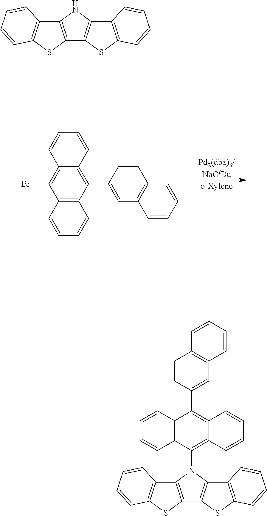


Claims (9)


Priority Applications (1)
| Application Number | Priority Date | Filing Date | Title |
|---|---|---|---|
| US16/532,512 US11524967B2 (en) | 2019-08-06 | 2019-08-06 | Heteroacene and organic electroluminescence device using the same |
Applications Claiming Priority (1)
| Application Number | Priority Date | Filing Date | Title |
|---|---|---|---|
| US16/532,512 US11524967B2 (en) | 2019-08-06 | 2019-08-06 | Heteroacene and organic electroluminescence device using the same |
Publications (2)
| Publication Number | Publication Date |
|---|---|
| US20210040112A1 US20210040112A1 (en) | 2021-02-11 |
| US11524967B2 true US11524967B2 (en) | 2022-12-13 |
Family
ID=74498329
Family Applications (1)
| Application Number | Title | Priority Date | Filing Date |
|---|---|---|---|
| US16/532,512 Active 2040-10-15 US11524967B2 (en) | 2019-08-06 | 2019-08-06 | Heteroacene and organic electroluminescence device using the same |
Country Status (1)
| Country | Link |
|---|---|
| US (1) | US11524967B2 (en) |
Families Citing this family (1)
| Publication number | Priority date | Publication date | Assignee | Title |
|---|---|---|---|---|
| CN113173932B (en) * | 2021-04-28 | 2022-09-16 | 武汉天马微电子有限公司 | Organic compound and electroluminescent application thereof |
Citations (4)
| Publication number | Priority date | Publication date | Assignee | Title |
|---|---|---|---|---|
| US20060263635A1 (en) * | 2005-05-06 | 2006-11-23 | Fuji Photo Film Co., Ltd. | Organic electroluminescent device |
| JP2007088016A (en) * | 2005-09-20 | 2007-04-05 | Konica Minolta Holdings Inc | Organic semiconductor material, organic semiconductor film, organic semiconductor device, organic thin-film transistor, and organic electroluminescent element |
| US20160322577A1 (en) * | 2015-04-28 | 2016-11-03 | Samsung Display Co., Ltd. | Compound and organic light-emitting device including the same |
| CN106831798A (en) * | 2017-01-25 | 2017-06-13 | 上海道亦化工科技有限公司 | Compound and its organic electroluminescence device containing five-membered ring structure |
-
2019
- 2019-08-06 US US16/532,512 patent/US11524967B2/en active Active
Patent Citations (4)
| Publication number | Priority date | Publication date | Assignee | Title |
|---|---|---|---|---|
| US20060263635A1 (en) * | 2005-05-06 | 2006-11-23 | Fuji Photo Film Co., Ltd. | Organic electroluminescent device |
| JP2007088016A (en) * | 2005-09-20 | 2007-04-05 | Konica Minolta Holdings Inc | Organic semiconductor material, organic semiconductor film, organic semiconductor device, organic thin-film transistor, and organic electroluminescent element |
| US20160322577A1 (en) * | 2015-04-28 | 2016-11-03 | Samsung Display Co., Ltd. | Compound and organic light-emitting device including the same |
| CN106831798A (en) * | 2017-01-25 | 2017-06-13 | 上海道亦化工科技有限公司 | Compound and its organic electroluminescence device containing five-membered ring structure |
Non-Patent Citations (2)
| Title |
|---|
| Machine English translation of Huang et al. (CN-106831798-A). Oct. 13, 2021. * |
| Machine English translation of Katakura et al. (JP-2007088016-A). Mar. 21, 2022. * |
Also Published As
| Publication number | Publication date |
|---|---|
| US20210040112A1 (en) | 2021-02-11 |
Similar Documents
| Publication | Publication Date | Title |
|---|---|---|
| US12490649B2 (en) | Organic light emitting diode and organic light emitting device including the same | |
| US12302756B2 (en) | Organic light emitting diode and organic light emitting device including the same | |
| US11482676B2 (en) | Light emitting diode including boron compound | |
| US12414460B2 (en) | Organic light emitting diode and organic light emitting device including the same | |
| US10562876B2 (en) | Organic compounds for organic light-emitting diode and organic light-emitting diode including the same | |
| US20210408390A1 (en) | Novel boron compound and organic light-emitting diode comprising same | |
| US12415950B2 (en) | Boron compound and organic light emitting diode including same | |
| US11038120B2 (en) | Organic compound and organic electroluminescence device using the same | |
| US9698351B2 (en) | Organic material for electroluminescent device | |
| US9893305B2 (en) | Indenotriphenylene-based iridium complexes for organic electroluminescence device | |
| US11563181B2 (en) | Amine compounds for organic light-emitting diode and organic light-emitting diode including the same | |
| US20210296589A1 (en) | Organic light emitting diode and organic light emitting device including the same | |
| US10636977B2 (en) | Light emitting material for organic electroluminescence device | |
| US10186668B2 (en) | Organic electroluminescent material and use thereof | |
| US20230159566A1 (en) | Novel boron compound and organic light-emitting diode comprising same | |
| US20190123284A1 (en) | Polyheteroaromatic compound and organic electroluminescence device using the same | |
| US10844043B2 (en) | Heteroaromatic compound and organic electroluminescence device using the same | |
| US20100308305A1 (en) | Organic luminescent material and organic light emitting device using the same | |
| US20120286251A1 (en) | Novel compound and organic light-emitting device including the same | |
| US11005047B2 (en) | Heteroaromatic compound and organic electroluminescence device using the same | |
| US9284486B2 (en) | Blue fluorescent composition and organic electroluminescent device using the same | |
| US20190273210A1 (en) | Heteroaromatic compound and organic electroluminescence device using the same | |
| US11524967B2 (en) | Heteroacene and organic electroluminescence device using the same | |
| US11380848B2 (en) | Organic compound and organic electroluminescence device using the same | |
| US11629140B2 (en) | Organic compound and organic electroluminescence device using the same |
Legal Events
| Date | Code | Title | Description |
|---|---|---|---|
| FEPP | Fee payment procedure |
Free format text: ENTITY STATUS SET TO UNDISCOUNTED (ORIGINAL EVENT CODE: BIG.); ENTITY STATUS OF PATENT OWNER: SMALL ENTITY |
|
| FEPP | Fee payment procedure |
Free format text: ENTITY STATUS SET TO SMALL (ORIGINAL EVENT CODE: SMAL); ENTITY STATUS OF PATENT OWNER: SMALL ENTITY |
|
| AS | Assignment |
Owner name: LUMINESCENCE TECHNOLOGY CORP., TAIWAN Free format text: ASSIGNMENT OF ASSIGNORS INTEREST;ASSIGNORS:YEN, FENG-WEN;HUANG, TSUN-YUAN;REEL/FRAME:053968/0294 Effective date: 20201005 |
|
| STPP | Information on status: patent application and granting procedure in general |
Free format text: NON FINAL ACTION MAILED |
|
| STPP | Information on status: patent application and granting procedure in general |
Free format text: RESPONSE TO NON-FINAL OFFICE ACTION ENTERED AND FORWARDED TO EXAMINER |
|
| STPP | Information on status: patent application and granting procedure in general |
Free format text: FINAL REJECTION MAILED |
|
| STPP | Information on status: patent application and granting procedure in general |
Free format text: RESPONSE AFTER FINAL ACTION FORWARDED TO EXAMINER |
|
| STPP | Information on status: patent application and granting procedure in general |
Free format text: ADVISORY ACTION MAILED |
|
| STPP | Information on status: patent application and granting procedure in general |
Free format text: RESPONSE AFTER FINAL ACTION FORWARDED TO EXAMINER |
|
| STPP | Information on status: patent application and granting procedure in general |
Free format text: ADVISORY ACTION MAILED |
|
| STPP | Information on status: patent application and granting procedure in general |
Free format text: RESPONSE AFTER FINAL ACTION FORWARDED TO EXAMINER |
|
| STPP | Information on status: patent application and granting procedure in general |
Free format text: NOTICE OF ALLOWANCE MAILED -- APPLICATION RECEIVED IN OFFICE OF PUBLICATIONS |
|
| STPP | Information on status: patent application and granting procedure in general |
Free format text: PUBLICATIONS -- ISSUE FEE PAYMENT RECEIVED |
|
| STPP | Information on status: patent application and granting procedure in general |
Free format text: PUBLICATIONS -- ISSUE FEE PAYMENT VERIFIED |
|
| STCF | Information on status: patent grant |
Free format text: PATENTED CASE |