US11521682B2 - Temperature compensation in an analog memory array by changing a threshold voltage of a selected memory cell in the array - Google Patents
Temperature compensation in an analog memory array by changing a threshold voltage of a selected memory cell in the array Download PDFInfo
- Publication number
- US11521682B2 US11521682B2 US17/095,661 US202017095661A US11521682B2 US 11521682 B2 US11521682 B2 US 11521682B2 US 202017095661 A US202017095661 A US 202017095661A US 11521682 B2 US11521682 B2 US 11521682B2
- Authority
- US
- United States
- Prior art keywords
- array
- memory cells
- cell
- memory cell
- memory
- Prior art date
- Legal status (The legal status is an assumption and is not a legal conclusion. Google has not performed a legal analysis and makes no representation as to the accuracy of the status listed.)
- Active
Links
Images


Classifications
-
- G—PHYSICS
- G11—INFORMATION STORAGE
- G11C—STATIC STORES
- G11C11/00—Digital stores characterised by the use of particular electric or magnetic storage elements; Storage elements therefor
- G11C11/54—Digital stores characterised by the use of particular electric or magnetic storage elements; Storage elements therefor using elements simulating biological cells, e.g. neuron
-
- G—PHYSICS
- G06—COMPUTING OR CALCULATING; COUNTING
- G06F—ELECTRIC DIGITAL DATA PROCESSING
- G06F17/00—Digital computing or data processing equipment or methods, specially adapted for specific functions
- G06F17/10—Complex mathematical operations
- G06F17/16—Matrix or vector computation, e.g. matrix-matrix or matrix-vector multiplication, matrix factorization
-
- G—PHYSICS
- G06—COMPUTING OR CALCULATING; COUNTING
- G06N—COMPUTING ARRANGEMENTS BASED ON SPECIFIC COMPUTATIONAL MODELS
- G06N3/00—Computing arrangements based on biological models
- G06N3/02—Neural networks
- G06N3/04—Architecture, e.g. interconnection topology
- G06N3/044—Recurrent networks, e.g. Hopfield networks
- G06N3/0442—Recurrent networks, e.g. Hopfield networks characterised by memory or gating, e.g. long short-term memory [LSTM] or gated recurrent units [GRU]
-
- G—PHYSICS
- G06—COMPUTING OR CALCULATING; COUNTING
- G06N—COMPUTING ARRANGEMENTS BASED ON SPECIFIC COMPUTATIONAL MODELS
- G06N3/00—Computing arrangements based on biological models
- G06N3/02—Neural networks
- G06N3/04—Architecture, e.g. interconnection topology
- G06N3/0464—Convolutional networks [CNN, ConvNet]
-
- G06N3/0635—
-
- G—PHYSICS
- G06—COMPUTING OR CALCULATING; COUNTING
- G06N—COMPUTING ARRANGEMENTS BASED ON SPECIFIC COMPUTATIONAL MODELS
- G06N3/00—Computing arrangements based on biological models
- G06N3/02—Neural networks
- G06N3/06—Physical realisation, i.e. hardware implementation of neural networks, neurons or parts of neurons
- G06N3/063—Physical realisation, i.e. hardware implementation of neural networks, neurons or parts of neurons using electronic means
- G06N3/065—Analogue means
-
- G—PHYSICS
- G11—INFORMATION STORAGE
- G11C—STATIC STORES
- G11C16/00—Erasable programmable read-only memories
- G11C16/02—Erasable programmable read-only memories electrically programmable
- G11C16/04—Erasable programmable read-only memories electrically programmable using variable threshold transistors, e.g. FAMOS
- G11C16/0408—Erasable programmable read-only memories electrically programmable using variable threshold transistors, e.g. FAMOS comprising cells containing floating gate transistors
- G11C16/0425—Erasable programmable read-only memories electrically programmable using variable threshold transistors, e.g. FAMOS comprising cells containing floating gate transistors comprising cells containing a merged floating gate and select transistor
-
- G—PHYSICS
- G11—INFORMATION STORAGE
- G11C—STATIC STORES
- G11C16/00—Erasable programmable read-only memories
- G11C16/02—Erasable programmable read-only memories electrically programmable
- G11C16/06—Auxiliary circuits, e.g. for writing into memory
- G11C16/10—Programming or data input circuits
- G11C16/14—Circuits for erasing electrically, e.g. erase voltage switching circuits
- G11C16/16—Circuits for erasing electrically, e.g. erase voltage switching circuits for erasing blocks, e.g. arrays, words, groups
-
- G—PHYSICS
- G11—INFORMATION STORAGE
- G11C—STATIC STORES
- G11C16/00—Erasable programmable read-only memories
- G11C16/02—Erasable programmable read-only memories electrically programmable
- G11C16/06—Auxiliary circuits, e.g. for writing into memory
- G11C16/26—Sensing or reading circuits; Data output circuits
-
- G—PHYSICS
- G11—INFORMATION STORAGE
- G11C—STATIC STORES
- G11C7/00—Arrangements for writing information into, or reading information out from, a digital store
- G11C7/04—Arrangements for writing information into, or reading information out from, a digital store with means for avoiding disturbances due to temperature effects
-
- G—PHYSICS
- G06—COMPUTING OR CALCULATING; COUNTING
- G06N—COMPUTING ARRANGEMENTS BASED ON SPECIFIC COMPUTATIONAL MODELS
- G06N3/00—Computing arrangements based on biological models
- G06N3/02—Neural networks
- G06N3/04—Architecture, e.g. interconnection topology
-
- G—PHYSICS
- G06—COMPUTING OR CALCULATING; COUNTING
- G06N—COMPUTING ARRANGEMENTS BASED ON SPECIFIC COMPUTATIONAL MODELS
- G06N3/00—Computing arrangements based on biological models
- G06N3/02—Neural networks
- G06N3/04—Architecture, e.g. interconnection topology
- G06N3/045—Combinations of networks
-
- G—PHYSICS
- G06—COMPUTING OR CALCULATING; COUNTING
- G06N—COMPUTING ARRANGEMENTS BASED ON SPECIFIC COMPUTATIONAL MODELS
- G06N3/00—Computing arrangements based on biological models
- G06N3/02—Neural networks
- G06N3/08—Learning methods
-
- G—PHYSICS
- G11—INFORMATION STORAGE
- G11C—STATIC STORES
- G11C2216/00—Indexing scheme relating to G11C16/00 and subgroups, for features not directly covered by these groups
- G11C2216/02—Structural aspects of erasable programmable read-only memories
- G11C2216/04—Nonvolatile memory cell provided with a separate control gate for erasing the cells, i.e. erase gate, independent of the normal read control gate
Definitions
- FIG. 33 depicts a system that compensates for differences in slope of the current-voltage characteristic curves of two devices in a system, such as reference memory cell and a selected memory cell.
- layer C 1 in the present example, there are 16 feature maps, with 30 ⁇ 30 pixels each. Each pixel is a new feature pixel extracted from multiplying the inputs and kernel, and therefore each feature map is a two dimensional array, and thus in this example layer C 1 constitutes 16 layers of two dimensional arrays (keeping in mind that the layers and arrays referenced herein are logical relationships, not necessarily physical relationships—i.e., the arrays are not necessarily oriented in physical two dimensional arrays). Each of the 16 feature maps in layer C 1 is generated by one of sixteen different sets of synapse weights applied to the filter scans. The C 1 feature maps could all be directed to different aspects of the same image feature, such as boundary identification.
- Non-volatile memory cell array 33 serves two purposes. First, it stores the weights that will be used by the VMM array 32 . Second, the non-volatile memory cell array 33 effectively multiplies the inputs by the weights stored in the non-volatile memory cell array 33 and adds them up per output line (source line or bit line) to produce the output, which will be the input to the next layer or input to the final layer. By performing the multiplication and addition function, the non-volatile memory cell array 33 negates the need for separate multiplication and addition logic circuits and is also power efficient due to its in-situ memory computation.
- the first and second non-volatile reference memory cells are diode-connected through multiplexors 1014 (only partially depicted) with current inputs flowing into them.
- the reference cells are tuned (e.g., programmed) to target reference levels.
- the target reference levels are provided by a reference mini-array matrix (not shown).
- Table No. 7 depicts operating voltages for VMM array 1200 .
- the columns in the table indicate the voltages placed on word lines for selected cells, word lines for unselected cells, bit lines for selected cells, bit lines for unselected cells, control gates for selected cells, control gates for unselected cells in the same sector as the selected cells, control gates for unselected cells in a different sector than the selected cells, erase gates for selected cells, erase gates for unselected cells, source lines for selected cells, and source lines for unselected cells.
- the rows indicate the operations of read, erase, and program.
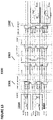
- FIG. 13 depicts neuron VMM array 1300 , which is particularly suited for memory cells 310 as shown in FIG. 3 , and is utilized as the synapses and parts of neurons between an input layer and the next layer.
- VMM array 1300 comprises a memory array 1303 of non-volatile memory cells, reference array 1301 or first non-volatile reference memory cells, and reference array 1302 of second non-volatile reference memory cells.
- EG lines EGR 0 , EG 0 , EG 1 and EGR 1 are run vertically while CG lines CG 0 , CG 1 , CG 2 and CG 3 and SL lines WL 0 , WL 1 , WL 2 and WL 3 are run horizontally.
- Each of the control bits 2403 is asserted during a certain temperature range assigned to that control bit. Thus, as temperature increases, a different control bit 2403 will be asserted as each discrete level of temperature is reached.
- the control bits 2403 are then applied to switches 2405 (which also number from 2405 a , . . . , 2405 i ) in FIG. 24 C , which depicts a temperature compensation bias voltage generation circuit.
- Each switch 2405 when closed, applies current source 2404 (which also number from 2404 a , . . . , 2404 i ) to one end of resistor 2406 .
- each current source 2404 generates a different amount of current than the current source 2404 that was activated by a switch at the preceding temperature range.
- Vtc is a temperature compensation bias voltage that can be applied to the gate of a transistor, the word line of a memory cell of the type shown in FIG. 2 as memory cell 210 , the control gate of a memory cell of the type shown in FIG. 3 as memory cell 310 , the source gate of a memory cell of the type shown in FIG. 4 as memory cell 410 , or the control gate of a memory cell of the type shown in FIG. 5 as memory cell 510 .
Landscapes
- Engineering & Computer Science (AREA)
- Physics & Mathematics (AREA)
- Theoretical Computer Science (AREA)
- Mathematical Physics (AREA)
- General Physics & Mathematics (AREA)
- Microelectronics & Electronic Packaging (AREA)
- Data Mining & Analysis (AREA)
- Health & Medical Sciences (AREA)
- Biomedical Technology (AREA)
- Life Sciences & Earth Sciences (AREA)
- Software Systems (AREA)
- Computing Systems (AREA)
- General Engineering & Computer Science (AREA)
- Molecular Biology (AREA)
- General Health & Medical Sciences (AREA)
- Biophysics (AREA)
- Computational Mathematics (AREA)
- Pure & Applied Mathematics (AREA)
- Mathematical Analysis (AREA)
- Mathematical Optimization (AREA)
- Computational Linguistics (AREA)
- Artificial Intelligence (AREA)
- Evolutionary Computation (AREA)
- Neurology (AREA)
- Databases & Information Systems (AREA)
- Algebra (AREA)
- Computer Hardware Design (AREA)
- Non-Volatile Memory (AREA)
- Read Only Memory (AREA)
- Complex Calculations (AREA)
Abstract
Description
| TABLE NO. 1 |
| Operation of |
| WL | BL | SL | |||
| Read | 2-3 | V | 0.6-2 | V | 0 | V | |
| Erase | ~11-13 | V | 0 | V | 0 | V | |
| Program | 1-2 | V | 1-3 | μA | 9-10 | V | |
| TABLE NO. 2 |
| Operation of |
| WL/SG | BL | CG | EG | SL | |
| Read | 1.0-2 | V | 0.6-2 | V | 0-2.6 | V | 0-2.6 | V | 0 | V |
| Erase | −0.5 V/0 V | 0 | V | 0 V/−8 V | 8-12 | V | 0 | V |
| Program | 1 | |
1 | μA | 8-11 | V | 4.5-9 | V | 4.5-5 | V |
| TABLE NO. 3 |
| Operation of |
| WL/SG | BL | EG | SL | ||||
| Read | 0.7-2.2 | V | 0.6-2 | V | 0-2.6 | V | 0 | V |
| Erase | −0.5 V/0 V | 0 | V | 11.5 | V | 0 | V |
| Program | 1 | V | 2-3 | μA | 4.5 | V | 7-9 | V |
| TABLE NO. 4 |
| Operation of |
| CG | BL | SL | Substrate | |
| Read | 2-5 V | 0.6-2 | V | 0 V | 0 V |
| Erase | −8 to −10 V/0 V | FLT | FLT | 8-10 V/15-20 V |
| Program | 8-12 V | 3-5 | V | 0 V | 0 V |
Ids=Io*e (Vg-Vth)/kVt =w*Io*e (Vg)/kvt,
-
- where w=e(−Vth)/kVt
Vg=k*Vt*log[Ids/wp*Io]
Here, wp is w of a reference or peripheral memory cell.
Iout=wa*Io*e (Vg)/kVt, namely
Iout=(wa/wp)*Iin=W*Iin
W=e (Vthp-Vtha)/kVt
Here, wa=w of each memory cell in the memory array.
Ids=beta*(Vgs−Vth)*Vds; beta=u*Cox*W/L
W=α(Vgs−Vth)
| TABLE 5 |
| Operation of |
| WL | WL-unsel | BL | BL-unsel | SL | SL-unsel | |
| Read | 1-3.5 | V | −0.5 V/0 V | 0.6-2 | V (Ineuron) | 0.6 V-2 V/0 V | 0 | V | 0 | V |
| Erase | ~5-13 | V | 0 V | 0 | V | 0 V | 0 | V | 0 | V |
| Program | 1-2 | V | −0.5 V/0 V | 0.1-3 | uA | Vinh ~2.5 V | 4-10 | V | 0-1 | V/FLT |
| TABLE NO. 6 |
| Operation of |
| WL - | BL - | SL - | |||||
| WL | unsel | BL | unsel | SL | unsel | ||
| Read | 1-3.5 | V | −0.5 V/0 V | 0.6-2 | V | 0.6 V-2 V/0 V | ~0.3-1 V | 0 | V |
| (Ineuron) |
| Erase | ~5-13 | V | 0 V | 0 | V | 0 V | 0 | V | SL-inhibit |
| (~4-8 V) |
| Program | 1-2 | V | −0.5 V/0 V | 0.1-3 | uA | Vinh ~2.5 V | 4-10 | V | 0-1 | V/FLT |
| TABLE NO. 7 |
| Operation of |
| CG - |
| unsel |
| WL - | BL - | same | CG - | EG - | SL - | |||||||
| WL | unsel | BL | unsel | CG | sector | unsel | EG | unsel | SL | unsel | ||
| Read | 1.0-2 | V | −0.5 V/0 V | 0.6-2 V | 0 V | 0-2.6 | V | 0-2.6 V | 0-2.6 V | 0-2.6 V | 0-2.6 V | 0 | V | 0 | V |
| (Ineuron) |
| Erase | 0 | V | 0 V | 0 | V | 0 V | 0 | V | 0-2.6 V | 0-2.6 V | 5-12 V | 0-2.6 V | 0 | V | 0 | V |
| Program | 0.7-1 | V | −0.5 V/0 V | 0.1-1 | uA | Vinh | 4-11 | V | 0-2.6 V | 0-2.6 V | 4.5-5 V | 0-2.6 V | 4.5-5 | V | 0-1 | V |
| (1-2 V) | ||||||||||||||||
| TABLE NO. 8 |
| Operation of |
| CG - |
| unsel |
| WL - | BL - | same | CG - | EG - | SL - | |||||||
| WL | unsel | BL | unsel | CG | sector | unsel | EG | unsel | SL | unsel | ||
| Read | 1.0-2 | V | −0.5 V/0 V | 0.6-2 V | 0 V | 0-2.6 | V | 0- 2.6 | V | 0-2.6 V | 0-2.6 V | 0-2.6 V | 0 | V | 0 | V |
| (Ineuron) |
| Erase | 0 | V | 0 V | 0 | V | 0 V | 0 | V | 4-9 | V | 0-2.6 V | 5-12 V | 0-2.6 V | 0 | V | 0 | V |
| Program | 0.7-1 | V | −0.5 V/0 V | 0.1-1 | uA | Vinh | 4-11 | V | 0-2.6 | V | 0-2.6 V | 4.5-5 V | 0-2.6 V | 4.5-5 | V | 0-1 | V |
| (1-2 V) | |||||||||||||||||
Ids=Ids0*exp(a*Vgs1−Vt)/(k*Vt), where Vt is thermal voltage.
Ids1=Ids0*exp(Vgs1−Vt)/k1*Ut
Ids2=Ids0*exp(Vgs2−Vt)/k2*Ut
Vgs1=a*Vgs2
This will mean that Ids1 and Ids will have the same slope after slope normalization.
Claims (12)
Priority Applications (1)
| Application Number | Priority Date | Filing Date | Title |
|---|---|---|---|
| US17/095,661 US11521682B2 (en) | 2018-08-27 | 2020-11-11 | Temperature compensation in an analog memory array by changing a threshold voltage of a selected memory cell in the array |
Applications Claiming Priority (4)
| Application Number | Priority Date | Filing Date | Title |
|---|---|---|---|
| US201862723398P | 2018-08-27 | 2018-08-27 | |
| US16/183,250 US10755783B2 (en) | 2018-08-27 | 2018-11-07 | Temperature and leakage compensation for memory cells in an analog neural memory system used in a deep learning neural network |
| US16/930,777 US11158374B2 (en) | 2018-08-27 | 2020-07-16 | Temperature compensation for memory cells in an analog neural memory system used in a deep learning neural network |
| US17/095,661 US11521682B2 (en) | 2018-08-27 | 2020-11-11 | Temperature compensation in an analog memory array by changing a threshold voltage of a selected memory cell in the array |
Related Parent Applications (1)
| Application Number | Title | Priority Date | Filing Date |
|---|---|---|---|
| US16/930,777 Continuation US11158374B2 (en) | 2018-08-27 | 2020-07-16 | Temperature compensation for memory cells in an analog neural memory system used in a deep learning neural network |
Publications (2)
| Publication Number | Publication Date |
|---|---|
| US20210090654A1 US20210090654A1 (en) | 2021-03-25 |
| US11521682B2 true US11521682B2 (en) | 2022-12-06 |
Family
ID=69586480
Family Applications (3)
| Application Number | Title | Priority Date | Filing Date |
|---|---|---|---|
| US16/183,250 Active 2038-11-23 US10755783B2 (en) | 2018-08-27 | 2018-11-07 | Temperature and leakage compensation for memory cells in an analog neural memory system used in a deep learning neural network |
| US16/930,777 Active US11158374B2 (en) | 2018-08-27 | 2020-07-16 | Temperature compensation for memory cells in an analog neural memory system used in a deep learning neural network |
| US17/095,661 Active US11521682B2 (en) | 2018-08-27 | 2020-11-11 | Temperature compensation in an analog memory array by changing a threshold voltage of a selected memory cell in the array |
Family Applications Before (2)
| Application Number | Title | Priority Date | Filing Date |
|---|---|---|---|
| US16/183,250 Active 2038-11-23 US10755783B2 (en) | 2018-08-27 | 2018-11-07 | Temperature and leakage compensation for memory cells in an analog neural memory system used in a deep learning neural network |
| US16/930,777 Active US11158374B2 (en) | 2018-08-27 | 2020-07-16 | Temperature compensation for memory cells in an analog neural memory system used in a deep learning neural network |
Country Status (7)
| Country | Link |
|---|---|
| US (3) | US10755783B2 (en) |
| EP (2) | EP4138079B1 (en) |
| JP (1) | JP7281535B2 (en) |
| KR (1) | KR102457394B1 (en) |
| CN (1) | CN112602095B (en) |
| TW (1) | TWI754162B (en) |
| WO (1) | WO2020046495A1 (en) |
Cited By (1)
| Publication number | Priority date | Publication date | Assignee | Title |
|---|---|---|---|---|
| US11716089B1 (en) * | 2022-03-16 | 2023-08-01 | Xilinx, Inc. | Delay-tracking biasing for voltage-to-time conversion |
Families Citing this family (19)
| Publication number | Priority date | Publication date | Assignee | Title |
|---|---|---|---|---|
| US10755783B2 (en) * | 2018-08-27 | 2020-08-25 | Silicon Storage Technology | Temperature and leakage compensation for memory cells in an analog neural memory system used in a deep learning neural network |
| US11513797B2 (en) * | 2018-09-12 | 2022-11-29 | Mentium Technologies Inc. | Systems and methods for analog vector by matrix multiplier |
| JP7196803B2 (en) * | 2018-10-18 | 2022-12-27 | 株式会社デンソー | Artificial Neural Network Circuit and Learning Value Switching Method in Artificial Neural Network Circuit |
| US11507641B2 (en) * | 2019-05-31 | 2022-11-22 | Advanced Micro Devices, Inc. | Temperature-based adjustments for in-memory matrix multiplication |
| US11074976B2 (en) * | 2019-08-26 | 2021-07-27 | Sandisk Technologies Llc | Temperature dependent impedance mitigation in non-volatile memory |
| US11875852B2 (en) * | 2020-07-06 | 2024-01-16 | Silicon Storage Technology, Inc. | Adaptive bias decoder to provide a voltage to a control gate line in an analog neural memory array in artificial neural network |
| US11809838B2 (en) * | 2020-09-08 | 2023-11-07 | Macronix International Co., Ltd. | Memory device and operation method thereof |
| US12106070B2 (en) * | 2020-09-08 | 2024-10-01 | Macronix International Co., Ltd. | Memory device and operation method thereof |
| US11630002B2 (en) * | 2021-02-08 | 2023-04-18 | Macronix International Co., Ltd. | Method for sensing temperature in memory die, memory die and memory with temperature sensing function |
| KR102553403B1 (en) * | 2021-02-23 | 2023-07-11 | 한국과학기술원 | Neuromorphic synapse device with excellent linearity characteristics and operating method thereof |
| US12572786B2 (en) | 2021-03-31 | 2026-03-10 | International Business Machines Corporation | NVM-based high-capacity neural network inference engine |
| US11521694B2 (en) * | 2021-05-04 | 2022-12-06 | Micron Technology, Inc. | Adjustment to trim settings based on a use of a memory device |
| US11380373B1 (en) * | 2021-05-12 | 2022-07-05 | Globalfoundries U.S. Inc. | Memory with read circuit for current-to-voltage slope characteristic-based sensing and method |
| US12579422B2 (en) * | 2021-08-02 | 2026-03-17 | Silicon Storage Technology, Inc. | Input circuitry for analog neural memory in a deep learning artificial neural network |
| US11989440B2 (en) * | 2021-08-11 | 2024-05-21 | Silicon Storage Technology, Inc. | Hybrid memory system configurable to store neural memory weight data in analog form or digital form |
| JP7733233B2 (en) * | 2021-11-12 | 2025-09-02 | シリコン ストーリッジ テクノロージー インコーポレイテッド | Determining bias voltages to apply to one or more memory cells in a neural network |
| US20230306246A1 (en) * | 2022-02-08 | 2023-09-28 | Silicon Storage Technology, Inc. | Calibration of electrical parameters in a deep learning artificial neural network |
| TWI852248B (en) * | 2022-12-29 | 2024-08-11 | 大陸商合肥創發微電子有限公司 | Method of dynamic compensation and a system thereof |
| US11955193B1 (en) * | 2023-12-05 | 2024-04-09 | Aspinity, Inc. | Compute-in-memory array multi-range temperature compensation |
Citations (17)
| Publication number | Priority date | Publication date | Assignee | Title |
|---|---|---|---|---|
| US3668440A (en) | 1970-10-16 | 1972-06-06 | Motorola Inc | Temperature stable monolithic multiplier circuit |
| US5029130A (en) | 1990-01-22 | 1991-07-02 | Silicon Storage Technology, Inc. | Single transistor non-valatile electrically alterable semiconductor memory device |
| US6359499B1 (en) | 2000-06-23 | 2002-03-19 | Marvell International Ltd. | Temperature and process independent CMOS circuit |
| US6560152B1 (en) | 2001-11-02 | 2003-05-06 | Sandisk Corporation | Non-volatile memory with temperature-compensated data read |
| US6747310B2 (en) | 2002-10-07 | 2004-06-08 | Actrans System Inc. | Flash memory cells with separated self-aligned select and erase gates, and process of fabrication |
| US7940577B2 (en) * | 2005-11-15 | 2011-05-10 | Renesas Electronics Corporation | Semiconductor integrated circuit device minimizing leakage current |
| US20120134213A1 (en) * | 2010-11-25 | 2012-05-31 | Samsung Electronics Co., Ltd. | Method compensation operating voltage, flash memory device, and data storage device |
| EP2690628A1 (en) | 2012-07-25 | 2014-01-29 | Freescale Semiconductor, Inc. | Methods and systems for adjusting NVM cell bias conditions based upon operating temperature to reduce performance degradation |
| US20150154910A1 (en) | 2013-11-29 | 2015-06-04 | Samsung Display Co., Ltd. | Display device, method of calculating compensation data thereof, and driving method thereof |
| US20150310938A1 (en) * | 2014-04-25 | 2015-10-29 | Seagate Technology Llc | Temperature Tracking to Manage Threshold Voltages in a Memory |
| US20170031259A1 (en) | 2015-07-28 | 2017-02-02 | Oce Printing Systems Gmbh & Co. Kg | Method and device for improving the toner transfer in an electrographic digital printer |
| US20170077182A1 (en) | 2015-09-15 | 2017-03-16 | The Regents Of The University Of California | Memristors and method for fabricating memristors |
| US20170337466A1 (en) | 2016-05-17 | 2017-11-23 | Silicon Storage Technology, Inc. | Deep Learning Neural Network Classifier Using Non-volatile Memory Array |
| US20170337980A1 (en) | 2016-05-17 | 2017-11-23 | Silicon Storage Technology, Inc. | Flash Memory Array With Individual Memory Cell Read, Program And Erase |
| US20180293029A1 (en) * | 2016-03-04 | 2018-10-11 | Western Digital Technologies, Inc. | Temperature variation compensation |
| US20190164617A1 (en) | 2017-11-29 | 2019-05-30 | Silicon Storage Technology, Inc. | High Precision And Highly Efficient Tuning Mechanisms And Algorithms For Analog Neuromorphic Memory In Artificial Neural Networks |
| US10528643B1 (en) * | 2018-08-01 | 2020-01-07 | Sandisk Technologies Llc | Vector-matrix multiplication using non-volatile memory cells |
Family Cites Families (9)
| Publication number | Priority date | Publication date | Assignee | Title |
|---|---|---|---|---|
| JP2007059024A (en) * | 2005-08-26 | 2007-03-08 | Micron Technol Inc | Method and apparatus for generating temperature compensated read and verify operations in flash memory |
| US8102201B2 (en) * | 2006-09-25 | 2012-01-24 | Analog Devices, Inc. | Reference circuit and method for providing a reference |
| ITRM20060652A1 (en) * | 2006-12-06 | 2008-06-07 | Micron Technology Inc | TEMPERATURE COMPENSATION OF MEMORY SIGNALS USING DIGITAL SIGNALS |
| US7889575B2 (en) * | 2008-09-22 | 2011-02-15 | Sandisk Corporation | On-chip bias voltage temperature coefficient self-calibration mechanism |
| CN102684683B (en) * | 2012-05-14 | 2014-07-02 | 常熟银海集成电路有限公司 | Any-item all-coefficient high-precision temperature compensation crystal oscillator |
| CN107533668B (en) * | 2016-03-11 | 2021-01-26 | 慧与发展有限责任合伙企业 | Hardware accelerator and method for calculating node values of a neural network |
| WO2018150295A1 (en) * | 2017-02-15 | 2018-08-23 | 株式会社半導体エネルギー研究所 | Semiconductor device |
| US11443175B2 (en) * | 2018-07-11 | 2022-09-13 | Silicon Storage Technology, Inc. | Compensation for reference transistors and memory cells in analog neuro memory in deep learning artificial neural network |
| US10755783B2 (en) * | 2018-08-27 | 2020-08-25 | Silicon Storage Technology | Temperature and leakage compensation for memory cells in an analog neural memory system used in a deep learning neural network |
-
2018
- 2018-11-07 US US16/183,250 patent/US10755783B2/en active Active
-
2019
- 2019-07-23 WO PCT/US2019/043101 patent/WO2020046495A1/en not_active Ceased
- 2019-07-23 JP JP2021510952A patent/JP7281535B2/en active Active
- 2019-07-23 CN CN201980055114.7A patent/CN112602095B/en active Active
- 2019-07-23 EP EP22201333.6A patent/EP4138079B1/en active Active
- 2019-07-23 KR KR1020217007006A patent/KR102457394B1/en active Active
- 2019-07-23 EP EP19790890.8A patent/EP3844680B1/en active Active
- 2019-08-20 TW TW108129667A patent/TWI754162B/en active
-
2020
- 2020-07-16 US US16/930,777 patent/US11158374B2/en active Active
- 2020-11-11 US US17/095,661 patent/US11521682B2/en active Active
Patent Citations (19)
| Publication number | Priority date | Publication date | Assignee | Title |
|---|---|---|---|---|
| US3668440A (en) | 1970-10-16 | 1972-06-06 | Motorola Inc | Temperature stable monolithic multiplier circuit |
| US5029130A (en) | 1990-01-22 | 1991-07-02 | Silicon Storage Technology, Inc. | Single transistor non-valatile electrically alterable semiconductor memory device |
| US6359499B1 (en) | 2000-06-23 | 2002-03-19 | Marvell International Ltd. | Temperature and process independent CMOS circuit |
| US6560152B1 (en) | 2001-11-02 | 2003-05-06 | Sandisk Corporation | Non-volatile memory with temperature-compensated data read |
| US6747310B2 (en) | 2002-10-07 | 2004-06-08 | Actrans System Inc. | Flash memory cells with separated self-aligned select and erase gates, and process of fabrication |
| US7940577B2 (en) * | 2005-11-15 | 2011-05-10 | Renesas Electronics Corporation | Semiconductor integrated circuit device minimizing leakage current |
| US20120134213A1 (en) * | 2010-11-25 | 2012-05-31 | Samsung Electronics Co., Ltd. | Method compensation operating voltage, flash memory device, and data storage device |
| US20140029335A1 (en) | 2012-07-25 | 2014-01-30 | Fuchen Mu | Methods and systems for adjusting nvm cell bias conditions based upon operating temperature to reduce performance degradation |
| EP2690628A1 (en) | 2012-07-25 | 2014-01-29 | Freescale Semiconductor, Inc. | Methods and systems for adjusting NVM cell bias conditions based upon operating temperature to reduce performance degradation |
| US20150154910A1 (en) | 2013-11-29 | 2015-06-04 | Samsung Display Co., Ltd. | Display device, method of calculating compensation data thereof, and driving method thereof |
| US20150310938A1 (en) * | 2014-04-25 | 2015-10-29 | Seagate Technology Llc | Temperature Tracking to Manage Threshold Voltages in a Memory |
| US20170031259A1 (en) | 2015-07-28 | 2017-02-02 | Oce Printing Systems Gmbh & Co. Kg | Method and device for improving the toner transfer in an electrographic digital printer |
| US20170077182A1 (en) | 2015-09-15 | 2017-03-16 | The Regents Of The University Of California | Memristors and method for fabricating memristors |
| US20180293029A1 (en) * | 2016-03-04 | 2018-10-11 | Western Digital Technologies, Inc. | Temperature variation compensation |
| US20170337466A1 (en) | 2016-05-17 | 2017-11-23 | Silicon Storage Technology, Inc. | Deep Learning Neural Network Classifier Using Non-volatile Memory Array |
| US20170337980A1 (en) | 2016-05-17 | 2017-11-23 | Silicon Storage Technology, Inc. | Flash Memory Array With Individual Memory Cell Read, Program And Erase |
| US20190164617A1 (en) | 2017-11-29 | 2019-05-30 | Silicon Storage Technology, Inc. | High Precision And Highly Efficient Tuning Mechanisms And Algorithms For Analog Neuromorphic Memory In Artificial Neural Networks |
| US10748630B2 (en) | 2017-11-29 | 2020-08-18 | Silicon Storage Technology, Inc. | High precision and highly efficient tuning mechanisms and algorithms for analog neuromorphic memory in artificial neural networks |
| US10528643B1 (en) * | 2018-08-01 | 2020-01-07 | Sandisk Technologies Llc | Vector-matrix multiplication using non-volatile memory cells |
Non-Patent Citations (4)
| Title |
|---|
| Bayat, et al., "Model-Based High-Precision Tuning of NOR Flash Memory Cells for Analog Computing Applications," 2016 74th Annual Device Research Conference, IEEE, Jun. 19, 2016, pp. 1-2. |
| Do, et al., "A 55 nm Logic-Process-Compatible, Split-Gate Flash Memory Array Fully Demonstrated at Automotive Temperature with High Access Speed and Reliability," IEEE International Memory Workshop, May 17-20, 2015, pp. 1-3. |
| European Examiner's Report dated Dec. 16, 2021 corresponding to the counterpart European Patent Application No. 19 790 890.8. |
| Guo, et al., "Temperature-Insensitive Analog Vector-by-Matrix Multiplier Based on 55 nm NOR Flash Memory Cells," IEEE, Apr. 30, 2017, pp. 1-4. |
Cited By (1)
| Publication number | Priority date | Publication date | Assignee | Title |
|---|---|---|---|---|
| US11716089B1 (en) * | 2022-03-16 | 2023-08-01 | Xilinx, Inc. | Delay-tracking biasing for voltage-to-time conversion |
Also Published As
| Publication number | Publication date |
|---|---|
| EP4138079A1 (en) | 2023-02-22 |
| US20210090654A1 (en) | 2021-03-25 |
| JP2021536623A (en) | 2021-12-27 |
| CN112602095B (en) | 2022-05-27 |
| EP3844680A1 (en) | 2021-07-07 |
| WO2020046495A1 (en) | 2020-03-05 |
| TW202026955A (en) | 2020-07-16 |
| US10755783B2 (en) | 2020-08-25 |
| KR102457394B1 (en) | 2022-10-21 |
| US20200350015A1 (en) | 2020-11-05 |
| TWI754162B (en) | 2022-02-01 |
| EP3844680B1 (en) | 2022-11-23 |
| CN112602095A (en) | 2021-04-02 |
| US11158374B2 (en) | 2021-10-26 |
| EP4138079B1 (en) | 2024-08-28 |
| JP7281535B2 (en) | 2023-05-25 |
| KR20210032538A (en) | 2021-03-24 |
| US20200066345A1 (en) | 2020-02-27 |
Similar Documents
| Publication | Publication Date | Title |
|---|---|---|
| US11521682B2 (en) | Temperature compensation in an analog memory array by changing a threshold voltage of a selected memory cell in the array | |
| US10896368B2 (en) | Analog neural memory system for deep learning neural network comprising multiple vector-by-matrix multiplication arrays and shared components | |
| US12198043B2 (en) | Output circuit | |
| US11354562B2 (en) | Programmable neuron for analog non-volatile memory in deep learning artificial neural network | |
| US11847557B2 (en) | Compensation for reference transistors and memory cells in analog neuro memory in deep learning artificial neural network | |
| US20210142854A1 (en) | Verifying or reading a cell in an analog neural memory in a deep learning artificial neural network | |
| US12444449B2 (en) | Output block for array of non-volatile memory cells | |
| US20260031112A1 (en) | Bitline regulation circuit | |
| US20230049032A1 (en) | Output circuitry for analog neural memory in a deep learning artificial neural network | |
| US12469523B2 (en) | Current-to-voltage converter comprising common mode circuit | |
| US20240119272A1 (en) | Voltage generator for analog neural memory array | |
| US20260031119A1 (en) | Output block for array of non-volatile memory cells | |
| US12566569B2 (en) | Array of non-volatile memory cells to store data in analog form and digital form |
Legal Events
| Date | Code | Title | Description |
|---|---|---|---|
| FEPP | Fee payment procedure |
Free format text: ENTITY STATUS SET TO UNDISCOUNTED (ORIGINAL EVENT CODE: BIG.); ENTITY STATUS OF PATENT OWNER: LARGE ENTITY |
|
| AS | Assignment |
Owner name: WELLS FARGO BANK, NATIONAL ASSOCIATION, AS COLLATERAL AGENT, MINNESOTA Free format text: SECURITY INTEREST;ASSIGNORS:MICROCHIP TECHNOLOGY INCORPORATED;SILICON STORAGE TECHNOLOGY, INC.;ATMEL CORPORATION;AND OTHERS;REEL/FRAME:055671/0612 Effective date: 20201217 |
|
| STPP | Information on status: patent application and granting procedure in general |
Free format text: DOCKETED NEW CASE - READY FOR EXAMINATION |
|
| AS | Assignment |
Owner name: WELLS FARGO BANK, NATIONAL ASSOCIATION, AS NOTES COLLATERAL AGENT, MINNESOTA Free format text: SECURITY INTEREST;ASSIGNORS:MICROCHIP TECHNOLOGY INCORPORATED;SILICON STORAGE TECHNOLOGY, INC.;ATMEL CORPORATION;AND OTHERS;REEL/FRAME:057935/0474 Effective date: 20210528 |
|
| STPP | Information on status: patent application and granting procedure in general |
Free format text: NON FINAL ACTION MAILED |
|
| STPP | Information on status: patent application and granting procedure in general |
Free format text: RESPONSE TO NON-FINAL OFFICE ACTION ENTERED AND FORWARDED TO EXAMINER |
|
| AS | Assignment |
Owner name: WELLS FARGO BANK, NATIONAL ASSOCIATION, AS NOTES COLLATERAL AGENT, MINNESOTA Free format text: GRANT OF SECURITY INTEREST IN PATENT RIGHTS;ASSIGNORS:MICROCHIP TECHNOLOGY INCORPORATED;SILICON STORAGE TECHNOLOGY, INC.;ATMEL CORPORATION;AND OTHERS;REEL/FRAME:058214/0625 Effective date: 20211117 Owner name: JPMORGAN CHASE BANK, N.A., AS ADMINISTRATIVE AGENT, ILLINOIS Free format text: GRANT OF SECURITY INTEREST IN PATENT RIGHTS;ASSIGNORS:MICROCHIP TECHNOLOGY INCORPORATED;SILICON STORAGE TECHNOLOGY, INC.;ATMEL CORPORATION;AND OTHERS;REEL/FRAME:058214/0380 Effective date: 20211117 Owner name: WELLS FARGO BANK, NATIONAL ASSOCIATION, AS NOTES COLLATERAL AGENT, MINNESOTA Free format text: GRANT OF SECURITY INTEREST IN PATENT RIGHTS;ASSIGNORS:MICROCHIP TECHNOLOGY INCORPORATED;SILICON STORAGE TECHNOLOGY, INC.;ATMEL CORPORATION;AND OTHERS;REEL/FRAME:058214/0238 Effective date: 20211117 |
|
| STPP | Information on status: patent application and granting procedure in general |
Free format text: FINAL REJECTION MAILED |
|
| STPP | Information on status: patent application and granting procedure in general |
Free format text: DOCKETED NEW CASE - READY FOR EXAMINATION |
|
| AS | Assignment |
Owner name: MICROSEMI STORAGE SOLUTIONS, INC., ARIZONA Free format text: RELEASE BY SECURED PARTY;ASSIGNOR:JPMORGAN CHASE BANK, N.A., AS ADMINISTRATIVE AGENT;REEL/FRAME:059264/0384 Effective date: 20220218 Owner name: MICROSEMI CORPORATION, ARIZONA Free format text: RELEASE BY SECURED PARTY;ASSIGNOR:JPMORGAN CHASE BANK, N.A., AS ADMINISTRATIVE AGENT;REEL/FRAME:059264/0384 Effective date: 20220218 Owner name: ATMEL CORPORATION, ARIZONA Free format text: RELEASE BY SECURED PARTY;ASSIGNOR:JPMORGAN CHASE BANK, N.A., AS ADMINISTRATIVE AGENT;REEL/FRAME:059264/0384 Effective date: 20220218 Owner name: SILICON STORAGE TECHNOLOGY, INC., ARIZONA Free format text: RELEASE BY SECURED PARTY;ASSIGNOR:JPMORGAN CHASE BANK, N.A., AS ADMINISTRATIVE AGENT;REEL/FRAME:059264/0384 Effective date: 20220218 Owner name: MICROCHIP TECHNOLOGY INCORPORATED, ARIZONA Free format text: RELEASE BY SECURED PARTY;ASSIGNOR:JPMORGAN CHASE BANK, N.A., AS ADMINISTRATIVE AGENT;REEL/FRAME:059264/0384 Effective date: 20220218 Owner name: MICROCHIP TECHNOLOGY INCORPORATED, ARIZONA Free format text: RELEASE OF SECURITY INTEREST;ASSIGNOR:JPMORGAN CHASE BANK, N.A., AS ADMINISTRATIVE AGENT;REEL/FRAME:059264/0384 Effective date: 20220218 Owner name: SILICON STORAGE TECHNOLOGY, INC., ARIZONA Free format text: RELEASE OF SECURITY INTEREST;ASSIGNOR:JPMORGAN CHASE BANK, N.A., AS ADMINISTRATIVE AGENT;REEL/FRAME:059264/0384 Effective date: 20220218 Owner name: ATMEL CORPORATION, ARIZONA Free format text: RELEASE OF SECURITY INTEREST;ASSIGNOR:JPMORGAN CHASE BANK, N.A., AS ADMINISTRATIVE AGENT;REEL/FRAME:059264/0384 Effective date: 20220218 Owner name: MICROSEMI CORPORATION, ARIZONA Free format text: RELEASE OF SECURITY INTEREST;ASSIGNOR:JPMORGAN CHASE BANK, N.A., AS ADMINISTRATIVE AGENT;REEL/FRAME:059264/0384 Effective date: 20220218 Owner name: MICROSEMI STORAGE SOLUTIONS, INC., ARIZONA Free format text: RELEASE OF SECURITY INTEREST;ASSIGNOR:JPMORGAN CHASE BANK, N.A., AS ADMINISTRATIVE AGENT;REEL/FRAME:059264/0384 Effective date: 20220218 |
|
| AS | Assignment |
Owner name: MICROSEMI STORAGE SOLUTIONS, INC., ARIZONA Free format text: RELEASE BY SECURED PARTY;ASSIGNOR:WELLS FARGO BANK, NATIONAL ASSOCIATION, AS NOTES COLLATERAL AGENT;REEL/FRAME:059357/0823 Effective date: 20220228 Owner name: MICROSEMI CORPORATION, ARIZONA Free format text: RELEASE BY SECURED PARTY;ASSIGNOR:WELLS FARGO BANK, NATIONAL ASSOCIATION, AS NOTES COLLATERAL AGENT;REEL/FRAME:059357/0823 Effective date: 20220228 Owner name: ATMEL CORPORATION, ARIZONA Free format text: RELEASE BY SECURED PARTY;ASSIGNOR:WELLS FARGO BANK, NATIONAL ASSOCIATION, AS NOTES COLLATERAL AGENT;REEL/FRAME:059357/0823 Effective date: 20220228 Owner name: SILICON STORAGE TECHNOLOGY, INC., ARIZONA Free format text: RELEASE BY SECURED PARTY;ASSIGNOR:WELLS FARGO BANK, NATIONAL ASSOCIATION, AS NOTES COLLATERAL AGENT;REEL/FRAME:059357/0823 Effective date: 20220228 Owner name: MICROCHIP TECHNOLOGY INCORPORATED, ARIZONA Free format text: RELEASE BY SECURED PARTY;ASSIGNOR:WELLS FARGO BANK, NATIONAL ASSOCIATION, AS NOTES COLLATERAL AGENT;REEL/FRAME:059357/0823 Effective date: 20220228 Owner name: MICROSEMI STORAGE SOLUTIONS, INC., ARIZONA Free format text: RELEASE BY SECURED PARTY;ASSIGNOR:WELLS FARGO BANK, NATIONAL ASSOCIATION, AS NOTES COLLATERAL AGENT;REEL/FRAME:059358/0335 Effective date: 20220228 Owner name: MICROSEMI CORPORATION, ARIZONA Free format text: RELEASE BY SECURED PARTY;ASSIGNOR:WELLS FARGO BANK, NATIONAL ASSOCIATION, AS NOTES COLLATERAL AGENT;REEL/FRAME:059358/0335 Effective date: 20220228 Owner name: ATMEL CORPORATION, ARIZONA Free format text: RELEASE BY SECURED PARTY;ASSIGNOR:WELLS FARGO BANK, NATIONAL ASSOCIATION, AS NOTES COLLATERAL AGENT;REEL/FRAME:059358/0335 Effective date: 20220228 Owner name: SILICON STORAGE TECHNOLOGY, INC., ARIZONA Free format text: RELEASE BY SECURED PARTY;ASSIGNOR:WELLS FARGO BANK, NATIONAL ASSOCIATION, AS NOTES COLLATERAL AGENT;REEL/FRAME:059358/0335 Effective date: 20220228 Owner name: MICROCHIP TECHNOLOGY INCORPORATED, ARIZONA Free format text: RELEASE BY SECURED PARTY;ASSIGNOR:WELLS FARGO BANK, NATIONAL ASSOCIATION, AS NOTES COLLATERAL AGENT;REEL/FRAME:059358/0335 Effective date: 20220228 Owner name: MICROCHIP TECHNOLOGY INCORPORATED, ARIZONA Free format text: RELEASE OF SECURITY INTEREST;ASSIGNOR:WELLS FARGO BANK, NATIONAL ASSOCIATION, AS NOTES COLLATERAL AGENT;REEL/FRAME:059357/0823 Effective date: 20220228 Owner name: SILICON STORAGE TECHNOLOGY, INC., ARIZONA Free format text: RELEASE OF SECURITY INTEREST;ASSIGNOR:WELLS FARGO BANK, NATIONAL ASSOCIATION, AS NOTES COLLATERAL AGENT;REEL/FRAME:059357/0823 Effective date: 20220228 Owner name: ATMEL CORPORATION, ARIZONA Free format text: RELEASE OF SECURITY INTEREST;ASSIGNOR:WELLS FARGO BANK, NATIONAL ASSOCIATION, AS NOTES COLLATERAL AGENT;REEL/FRAME:059357/0823 Effective date: 20220228 Owner name: MICROSEMI CORPORATION, ARIZONA Free format text: RELEASE OF SECURITY INTEREST;ASSIGNOR:WELLS FARGO BANK, NATIONAL ASSOCIATION, AS NOTES COLLATERAL AGENT;REEL/FRAME:059357/0823 Effective date: 20220228 Owner name: MICROSEMI STORAGE SOLUTIONS, INC., ARIZONA Free format text: RELEASE OF SECURITY INTEREST;ASSIGNOR:WELLS FARGO BANK, NATIONAL ASSOCIATION, AS NOTES COLLATERAL AGENT;REEL/FRAME:059357/0823 Effective date: 20220228 Owner name: MICROCHIP TECHNOLOGY INCORPORATED, ARIZONA Free format text: RELEASE OF SECURITY INTEREST;ASSIGNOR:WELLS FARGO BANK, NATIONAL ASSOCIATION, AS NOTES COLLATERAL AGENT;REEL/FRAME:059358/0335 Effective date: 20220228 Owner name: SILICON STORAGE TECHNOLOGY, INC., ARIZONA Free format text: RELEASE OF SECURITY INTEREST;ASSIGNOR:WELLS FARGO BANK, NATIONAL ASSOCIATION, AS NOTES COLLATERAL AGENT;REEL/FRAME:059358/0335 Effective date: 20220228 Owner name: ATMEL CORPORATION, ARIZONA Free format text: RELEASE OF SECURITY INTEREST;ASSIGNOR:WELLS FARGO BANK, NATIONAL ASSOCIATION, AS NOTES COLLATERAL AGENT;REEL/FRAME:059358/0335 Effective date: 20220228 Owner name: MICROSEMI CORPORATION, ARIZONA Free format text: RELEASE OF SECURITY INTEREST;ASSIGNOR:WELLS FARGO BANK, NATIONAL ASSOCIATION, AS NOTES COLLATERAL AGENT;REEL/FRAME:059358/0335 Effective date: 20220228 Owner name: MICROSEMI STORAGE SOLUTIONS, INC., ARIZONA Free format text: RELEASE OF SECURITY INTEREST;ASSIGNOR:WELLS FARGO BANK, NATIONAL ASSOCIATION, AS NOTES COLLATERAL AGENT;REEL/FRAME:059358/0335 Effective date: 20220228 |
|
| AS | Assignment |
Owner name: MICROSEMI STORAGE SOLUTIONS, INC., ARIZONA Free format text: RELEASE BY SECURED PARTY;ASSIGNOR:WELLS FARGO BANK, NATIONAL ASSOCIATION, AS NOTES COLLATERAL AGENT;REEL/FRAME:059863/0400 Effective date: 20220228 Owner name: MICROSEMI CORPORATION, ARIZONA Free format text: RELEASE BY SECURED PARTY;ASSIGNOR:WELLS FARGO BANK, NATIONAL ASSOCIATION, AS NOTES COLLATERAL AGENT;REEL/FRAME:059863/0400 Effective date: 20220228 Owner name: ATMEL CORPORATION, ARIZONA Free format text: RELEASE BY SECURED PARTY;ASSIGNOR:WELLS FARGO BANK, NATIONAL ASSOCIATION, AS NOTES COLLATERAL AGENT;REEL/FRAME:059863/0400 Effective date: 20220228 Owner name: SILICON STORAGE TECHNOLOGY, INC., ARIZONA Free format text: RELEASE BY SECURED PARTY;ASSIGNOR:WELLS FARGO BANK, NATIONAL ASSOCIATION, AS NOTES COLLATERAL AGENT;REEL/FRAME:059863/0400 Effective date: 20220228 Owner name: MICROCHIP TECHNOLOGY INCORPORATED, ARIZONA Free format text: RELEASE BY SECURED PARTY;ASSIGNOR:WELLS FARGO BANK, NATIONAL ASSOCIATION, AS NOTES COLLATERAL AGENT;REEL/FRAME:059863/0400 Effective date: 20220228 Owner name: MICROCHIP TECHNOLOGY INCORPORATED, ARIZONA Free format text: RELEASE OF SECURITY INTEREST;ASSIGNOR:WELLS FARGO BANK, NATIONAL ASSOCIATION, AS NOTES COLLATERAL AGENT;REEL/FRAME:059863/0400 Effective date: 20220228 Owner name: SILICON STORAGE TECHNOLOGY, INC., ARIZONA Free format text: RELEASE OF SECURITY INTEREST;ASSIGNOR:WELLS FARGO BANK, NATIONAL ASSOCIATION, AS NOTES COLLATERAL AGENT;REEL/FRAME:059863/0400 Effective date: 20220228 Owner name: ATMEL CORPORATION, ARIZONA Free format text: RELEASE OF SECURITY INTEREST;ASSIGNOR:WELLS FARGO BANK, NATIONAL ASSOCIATION, AS NOTES COLLATERAL AGENT;REEL/FRAME:059863/0400 Effective date: 20220228 Owner name: MICROSEMI CORPORATION, ARIZONA Free format text: RELEASE OF SECURITY INTEREST;ASSIGNOR:WELLS FARGO BANK, NATIONAL ASSOCIATION, AS NOTES COLLATERAL AGENT;REEL/FRAME:059863/0400 Effective date: 20220228 Owner name: MICROSEMI STORAGE SOLUTIONS, INC., ARIZONA Free format text: RELEASE OF SECURITY INTEREST;ASSIGNOR:WELLS FARGO BANK, NATIONAL ASSOCIATION, AS NOTES COLLATERAL AGENT;REEL/FRAME:059863/0400 Effective date: 20220228 |
|
| AS | Assignment |
Owner name: MICROSEMI STORAGE SOLUTIONS, INC., ARIZONA Free format text: RELEASE BY SECURED PARTY;ASSIGNOR:WELLS FARGO BANK, NATIONAL ASSOCIATION, AS NOTES COLLATERAL AGENT;REEL/FRAME:059363/0001 Effective date: 20220228 Owner name: MICROSEMI CORPORATION, ARIZONA Free format text: RELEASE BY SECURED PARTY;ASSIGNOR:WELLS FARGO BANK, NATIONAL ASSOCIATION, AS NOTES COLLATERAL AGENT;REEL/FRAME:059363/0001 Effective date: 20220228 Owner name: ATMEL CORPORATION, ARIZONA Free format text: RELEASE BY SECURED PARTY;ASSIGNOR:WELLS FARGO BANK, NATIONAL ASSOCIATION, AS NOTES COLLATERAL AGENT;REEL/FRAME:059363/0001 Effective date: 20220228 Owner name: SILICON STORAGE TECHNOLOGY, INC., ARIZONA Free format text: RELEASE BY SECURED PARTY;ASSIGNOR:WELLS FARGO BANK, NATIONAL ASSOCIATION, AS NOTES COLLATERAL AGENT;REEL/FRAME:059363/0001 Effective date: 20220228 Owner name: MICROCHIP TECHNOLOGY INCORPORATED, ARIZONA Free format text: RELEASE BY SECURED PARTY;ASSIGNOR:WELLS FARGO BANK, NATIONAL ASSOCIATION, AS NOTES COLLATERAL AGENT;REEL/FRAME:059363/0001 Effective date: 20220228 Owner name: MICROCHIP TECHNOLOGY INCORPORATED, ARIZONA Free format text: RELEASE OF SECURITY INTEREST;ASSIGNOR:WELLS FARGO BANK, NATIONAL ASSOCIATION, AS NOTES COLLATERAL AGENT;REEL/FRAME:059363/0001 Effective date: 20220228 Owner name: SILICON STORAGE TECHNOLOGY, INC., ARIZONA Free format text: RELEASE OF SECURITY INTEREST;ASSIGNOR:WELLS FARGO BANK, NATIONAL ASSOCIATION, AS NOTES COLLATERAL AGENT;REEL/FRAME:059363/0001 Effective date: 20220228 Owner name: ATMEL CORPORATION, ARIZONA Free format text: RELEASE OF SECURITY INTEREST;ASSIGNOR:WELLS FARGO BANK, NATIONAL ASSOCIATION, AS NOTES COLLATERAL AGENT;REEL/FRAME:059363/0001 Effective date: 20220228 Owner name: MICROSEMI CORPORATION, ARIZONA Free format text: RELEASE OF SECURITY INTEREST;ASSIGNOR:WELLS FARGO BANK, NATIONAL ASSOCIATION, AS NOTES COLLATERAL AGENT;REEL/FRAME:059363/0001 Effective date: 20220228 Owner name: MICROSEMI STORAGE SOLUTIONS, INC., ARIZONA Free format text: RELEASE OF SECURITY INTEREST;ASSIGNOR:WELLS FARGO BANK, NATIONAL ASSOCIATION, AS NOTES COLLATERAL AGENT;REEL/FRAME:059363/0001 Effective date: 20220228 |
|
| STPP | Information on status: patent application and granting procedure in general |
Free format text: NON FINAL ACTION MAILED |
|
| STPP | Information on status: patent application and granting procedure in general |
Free format text: RESPONSE TO NON-FINAL OFFICE ACTION ENTERED AND FORWARDED TO EXAMINER |
|
| STPP | Information on status: patent application and granting procedure in general |
Free format text: NOTICE OF ALLOWANCE MAILED -- APPLICATION RECEIVED IN OFFICE OF PUBLICATIONS |
|
| STPP | Information on status: patent application and granting procedure in general |
Free format text: PUBLICATIONS -- ISSUE FEE PAYMENT VERIFIED |
|
| STCF | Information on status: patent grant |
Free format text: PATENTED CASE |