US11520724B2 - Application-transparent near-memory processing architecture with memory channel network - Google Patents
Application-transparent near-memory processing architecture with memory channel network Download PDFInfo
- Publication number
- US11520724B2 US11520724B2 US17/250,785 US201917250785A US11520724B2 US 11520724 B2 US11520724 B2 US 11520724B2 US 201917250785 A US201917250785 A US 201917250785A US 11520724 B2 US11520724 B2 US 11520724B2
- Authority
- US
- United States
- Prior art keywords
- mcn
- memory
- host
- buffer
- network
- Prior art date
- Legal status (The legal status is an assumption and is not a legal conclusion. Google has not performed a legal analysis and makes no representation as to the accuracy of the status listed.)
- Active
Links
Images


Classifications
-
- G—PHYSICS
- G06—COMPUTING OR CALCULATING; COUNTING
- G06F—ELECTRIC DIGITAL DATA PROCESSING
- G06F13/00—Interconnection of, or transfer of information or other signals between, memories, input/output devices or central processing units
- G06F13/38—Information transfer, e.g. on bus
- G06F13/40—Bus structure
- G06F13/4004—Coupling between buses
- G06F13/4027—Coupling between buses using bus bridges
-
- G—PHYSICS
- G06—COMPUTING OR CALCULATING; COUNTING
- G06F—ELECTRIC DIGITAL DATA PROCESSING
- G06F13/00—Interconnection of, or transfer of information or other signals between, memories, input/output devices or central processing units
- G06F13/14—Handling requests for interconnection or transfer
- G06F13/16—Handling requests for interconnection or transfer for access to memory bus
- G06F13/1605—Handling requests for interconnection or transfer for access to memory bus based on arbitration
- G06F13/1647—Handling requests for interconnection or transfer for access to memory bus based on arbitration with interleaved bank access
-
- G—PHYSICS
- G06—COMPUTING OR CALCULATING; COUNTING
- G06F—ELECTRIC DIGITAL DATA PROCESSING
- G06F12/00—Accessing, addressing or allocating within memory systems or architectures
- G06F12/02—Addressing or allocation; Relocation
- G06F12/08—Addressing or allocation; Relocation in hierarchically structured memory systems, e.g. virtual memory systems
- G06F12/10—Address translation
-
- G—PHYSICS
- G06—COMPUTING OR CALCULATING; COUNTING
- G06F—ELECTRIC DIGITAL DATA PROCESSING
- G06F13/00—Interconnection of, or transfer of information or other signals between, memories, input/output devices or central processing units
- G06F13/14—Handling requests for interconnection or transfer
- G06F13/16—Handling requests for interconnection or transfer for access to memory bus
- G06F13/1668—Details of memory controller
- G06F13/1673—Details of memory controller using buffers
-
- G—PHYSICS
- G06—COMPUTING OR CALCULATING; COUNTING
- G06F—ELECTRIC DIGITAL DATA PROCESSING
- G06F12/00—Accessing, addressing or allocating within memory systems or architectures
- G06F12/02—Addressing or allocation; Relocation
- G06F12/06—Addressing a physical block of locations, e.g. base addressing, module addressing, memory dedication
- G06F12/0607—Interleaved addressing
-
- G—PHYSICS
- G06—COMPUTING OR CALCULATING; COUNTING
- G06F—ELECTRIC DIGITAL DATA PROCESSING
- G06F12/00—Accessing, addressing or allocating within memory systems or architectures
- G06F12/02—Addressing or allocation; Relocation
- G06F12/08—Addressing or allocation; Relocation in hierarchically structured memory systems, e.g. virtual memory systems
- G06F12/10—Address translation
- G06F12/1072—Decentralised address translation, e.g. in distributed shared memory systems
-
- G—PHYSICS
- G06—COMPUTING OR CALCULATING; COUNTING
- G06F—ELECTRIC DIGITAL DATA PROCESSING
- G06F2212/00—Indexing scheme relating to accessing, addressing or allocation within memory systems or architectures
- G06F2212/10—Providing a specific technical effect
- G06F2212/1016—Performance improvement
-
- Y—GENERAL TAGGING OF NEW TECHNOLOGICAL DEVELOPMENTS; GENERAL TAGGING OF CROSS-SECTIONAL TECHNOLOGIES SPANNING OVER SEVERAL SECTIONS OF THE IPC; TECHNICAL SUBJECTS COVERED BY FORMER USPC CROSS-REFERENCE ART COLLECTIONS [XRACs] AND DIGESTS
- Y02—TECHNOLOGIES OR APPLICATIONS FOR MITIGATION OR ADAPTATION AGAINST CLIMATE CHANGE
- Y02D—CLIMATE CHANGE MITIGATION TECHNOLOGIES IN INFORMATION AND COMMUNICATION TECHNOLOGIES [ICT], I.E. INFORMATION AND COMMUNICATION TECHNOLOGIES AIMING AT THE REDUCTION OF THEIR OWN ENERGY USE
- Y02D10/00—Energy efficient computing, e.g. low power processors, power management or thermal management
Definitions
- FIG. 1 A is a block diagram of an exemplary computing system in which a memory sub-system includes memory channel network (MCN) memory modules according to one embodiment.
- MCN memory channel network
- FIG. 1 B is a block diagram of one of the MCN memory modules of FIG. 1 A according to an embodiment.
- FIG. 1 C is a block diagram of an MCN processor disposed on the MCN module of FIG. 1 B according to an embodiment.
- FIG. 2 is a block diagram that illustrates functionality of a conventional network interface card (NIC) according to various embodiments.
- NIC network interface card
- FIG. 3 A is a graph diagram illustrative of a local buffer of the MCN processor of FIG. 1 C according to an embodiment.
- FIG. 3 B is a graph diagram illustrative of an MCN message stored in the local buffer according to an embodiment.
- FIG. 4 is a functional flow diagram illustrative of a relationship between the memory channel network hardware, kernel space software, and user space applications according to an embodiment.
- FIG. 5 is a flow chart of a method for handling a network packet received at an MCN-side interface from the network stack according to various embodiments.
- FIG. 6 is a flow chart of a method for a host-side polling agent to determine whether local buffers of MCN processors are attempting to transmit data according to various embodiments.
- FIG. 7 is a flow chart of a method for the host processor to decide where to route a network packet depending on its medium access control (MAC) address according to various embodiments.
- MAC medium access control
- FIG. 8 is a set of graphs illustrative of host processor view of interleaved arrangement of physical address space versus MCN processor views of that physical address space according to an embodiment.
- FIG. 9 A is an image of a ConTutto field programmable gate array (FPGA) board according to an embodiment.
- FPGA field programmable gate array
- FIG. 9 B is an image of the board of FIG. 8 A plugged into an International Business Machine (IBM S824L) system alongside regular Centaur DIMMs according to an embodiment.
- IBM S824L International Business Machine
- FIG. 9 C is a block diagram of an implementation example of the computing system of FIGS. 1 A- 1 C according to an embodiment.
- FIG. 10 is a block diagram of an example computer system in which embodiments of the present disclosure can operate.
- MCN Memory Channel Network
- DDR double data rate
- MCN architecture aims to give the host and near-memory processors connected through a host interface (such as a DDR interface) in a server the illusion that these processors connect through Ethernet links.
- MCN can provide a standard and application-transparent communication interface not only between the host and near-memory processors in a server, but also among such servers, seamlessly unifying near-memory processing with distributed computing for data-intensive applications.
- the MCN is made up of a combination of hardware and software.
- the hardware may include, but is not limited to, a memory module made MCN-capable with an MCN processor that will be explained in detail.
- the memory module may be a dual in-line memory module (DIMM) where memory components are coupled to the MCN processor on a substrate such as a printed circuit board (PCB) or the like.
- DIMM dual in-line memory module
- This “MCN DIMM” may be coupled between a host-side memory controller (MC) of a host computing system and installed DRAM devices, where the MCN processor may be viewed as a buffered device and the MCN DIMM as a buffered DIMM.
- Coupled to generally refers to a connection between components or devices, which can be an indirect communicative connection or direct communicative connection (e.g., without intervening components or devices), whether wired or wireless, including connections such as electrical, optical, magnetic, etc.
- an MCN interface may be implemented within the MCN processor to function similar to a network interface.
- MCN may build on any PHY for memory, including DDR PHY, GEN-ZTM PHY, or OpenCAPITM PHY, to interface between a host-side MC and the MCN processor.
- the MCN processor runs a lightweight operating system (OS) with the network software layer used for running a distributed computing framework.
- OS operating system
- the MCN may also deploy software on both the host system and the MCN processor, to facilitate data exchange between the two within the memory channel network.
- both the MCN and host processors may execute special MCN-adapted drivers.
- the MCN processor may execute an MCN driver
- the host processor may execute a corresponding (similar) MCN driver, referred to herein as a host MCN driver (or just “host driver” for simplicity).
- host MCN driver or just “host driver” for simplicity.
- the host driver running on the host processor may be similar to a conventional NIC driver but intercepts a network packet from the network software layer in the OS and redirects the network packet to a memory controller (MC) of an MCN DIMM if the network packet is destined (e.g., addressed) to the MCN DIMM.
- MC memory controller
- the memory interface (and MC) do not have a corresponding mechanism.
- the host driver is adapted with a mechanism (or mechanisms) to determine whether any MCN DIMM is sending a network packet to the host or other MCN DIMMs, as will be discussed.
- these MCN DIMMs and associated MCN drivers together allow a server to run an application based on a distributed computing framework without any change in the host processor hardware, distributed computing middleware, and application software, while offering the benefits of high-bandwidth and low-latency communications between the host and the MCN processors over memory channels.
- each MCN processor accesses its DRAM devices on the same MCN DIMM through a local memory channel that is isolated from a global memory channel shared with other DIMMs and the host. Therefore, multiple MCN DIMMs can concurrently operate. That is, the aggregate memory bandwidth for processing is proportional to the number of MCN DIMMs, and thus grows as the number of MCN DIMMs is increased.
- MCN architecture can serve as an application-transparent near memory processing platform, as well as unify near-memory processing in a server with the distributed computing across multiple servers.
- MCN architecture can unify near-DRAM processing in a node with distributed computing across multiple such nodes.
- optional software and hardware optimization techniques may be implemented. Specifically, the MCN driver and some of the OS network layers may be optimized, leveraging unique properties of MCN over traditional Ethernet. Further communication efficiency may be achieved by adapting an already existing signal from the memory components to the host in order to interrupt the host MC when an MCN DIMM has outgoing packets, to reduce polling cycles.
- a rack as the basic building block of a datacenter, includes several servers connected together using a top of rack switch.
- the bandwidth of a top of rack switch ranges from 1 to 10 Gbps, while the top of rack switches are connected together through 40 to 100 Gbps connections.
- MCN-enabled servers that interconnect leaf nodes (e.g., MCN nodes) using a low cost, energy efficient interconnect to improve the energy efficiency of running I/O intensive applications while reducing the datacenter cost.
- FIG. 1 A is a block diagram of an exemplary computing system 100 in which a memory sub-system 110 includes memory channel network (MCN) memory modules according to one embodiment.
- the computing system 100 may further include a host system 120 including a host processor 122 and a memory controller (MC) for each bank of memory modules.
- a (first) host MC 130 A and a (second) host MC 130 B are illustrated.
- the host processor 122 may execute a host operating system (OS) 125 and a host driver 127 (e.g., host MCN driver), as will be explained.
- OS host operating system
- a host driver 127 e.g., host MCN driver
- the memory sub-system 110 may include a number of memory modules, e.g., organized in banks that are coupled, via global memory channels 102 A and 102 B, to the host MC 130 A and the host MC 130 B, respectively. While only two global memory channels 102 A and 102 B are illustrated, it is to be understood that there could be multiple global memory channels more than what is illustrated.
- a first bank of DIMMS coupled to the host MC 130 A may include a first conventional (CONV) DIMM 112 A, a second CONV DIMM 114 A, a first MCN DIMM 116 A, and a second MCN DIMM 118 A.
- a second bank of DIMMS coupled to the host MC 130 B may include a first CONV DIMM 112 B, a second CONV DIMM 114 B, a first MCN DIMM 116 B, and a second MCN DIMM 118 B.
- the convention (or CONV) DIMMs employ the DDR protocol, although other high-bandwidth, low-latency protocols are also envisioned.
- the CONV DIMMs are DDR4 DIMMs, or other updated DIMM technology, in various embodiments.
- the host MC 130 A or 130 B treats MCN DIMMs as buffered DIMMs and thus supports a mixture of multiple MCN and conventional DIMMs per memory channel.
- a global memory channel couples an MC to one or more DIMMs.
- an MC drives hundreds of DRAM devices and delivers Command/Address (C/A) signals through the global memory channel to the DRAM devices.
- C/A Command/Address
- GHz gigahertz
- a C/A pin from a memory controller has to drive 144 DRAM devices (18 ⁇ 4 devices per rank supporting ECC multiplied by 8 ranks) when 8 ranks are populated per channel.
- a data pin is connected to 8 DRAM devices, which is an order of magnitude fewer. Therefore, DIMMs for servers typically employ a buffer per DIMM, such as Registered DIMM (RDIMM) or Load-Reduce DIMM (LRDIMM), to reduce this huge capacitive load imposed to an MC and alleviate the signal integrity problem.
- RDIMM Registered DIMM
- LDDIMM Load-Reduce DIMM
- a server may deploy another DIMM type with a buffer, e.g., a Centaur DIMM (CDIMM).
- Centaur is a memory buffer chip designed by IBM® for their POWER scale-up microprocessors.
- Each CDIMM with a tall form factor includes up to 80 commodity DDR DRAM devices and a Centaur device that provides a 16 MB eDRAM L4 cache, memory management logic, and an interface between DDR and IBM® proprietary memory interfaces. Note that the bandwidth available to the CPU remains constant as the global memory channel is shared by all the DIMMs although the memory capacity increases with more DIMMs per channel.
- the host system 120 may execute the host OS 125 and perform memory management for kernel space drivers.
- the host OS 125 can manage hierarchical page tables, each with two or more levels, depending on a processor architecture.
- the Linux kernel is responsible for setting up page tables and turning on a Memory Management Unit (MMU).
- MMU Memory Management Unit
- host OS 125 may want to reserve a specific range of physical memory space exclusively for a (memory-mapped) I/O device and its I/O driver, and allow the I/O driver to access this physical memory range with virtual addresses since every address issued by the processor is a virtual address after the MMU is turned on.
- a DTB is a set of attributes of the hardware components in a given system and is fetched during the booting process. Specifically, a node in a DTB represents a hardware component and describes information such as the number and type of CPUs, base physical addresses and sizes of memory devices, I/O devices, and the like.
- the host OS 125 may create a new node in the device tree, where a physical address range is explicitly enumerated and is tagged as reserved memory. At boot time, the kernel will exclude this physical address range from mapping to other processes, thereby creating a memory map hole. Later, the reserved memory region may be assigned to a device driver by setting the memory region (e.g., memory_region) parameter.
- the host OS 125 may also execute software to instantiate an OS network layer.
- Transport Control Protocol/Internet Protocol (TCP/IP) is the most commonly used protocol for the distributed computing frameworks.
- An application sends and receives data through a TCP socket, e.g., using tcp_sendmsg() and tcp_recvmsg() system calls, respectively.
- tcp_sendmsg() When a user application calls tcp_sendmsg() the data is copied to a kernel buffer, fragmented into several segments of Maximum Transmission Unit (MTU) size, undergoes TCP/IP processing, and is eventually sent to a NIC for transmission.
- MTU Maximum Transmission Unit
- a maximum transmission unit is the largest size packet or frame, specified in octets (eight-bit bytes), that can be sent in a packet- or frame-based network such as the Internet.
- the MTU limit exists since sending a packet with huge data at once is vulnerable to random transient errors in traditional physical links such as the Ethernet links, and increases the probability and the overhead of re-transmitting the packet.
- the default value of MTU is 1,500 bytes.
- the segments of a message are reassembled inside the Linux kernel and the complete message is copied to the user-space application.
- FIG. 2 is a block diagram that illustrates functionality of a network interface card (NIC) 205 according to various embodiments, where the NIC 205 may be a conventional NIC. More specifically, FIG. 2 illustrates the interactions between a processor 201 , physical memory 210 , and the NIC 205 when a network packet is received or transmitted. Once an outgoing network packet is processed in the TCP/IP stack, the network packet is written to a transmission (TX) ring buffer 214 (A) in the physical memory 210 . Then, a NIC driver executed on the processor 201 informs the NIC 205 of the available packets in the TX ring buffer 214 (B).
- TX transmission
- the NIC 205 reads the ready-to-transmit descriptors from the TX ring buffer 214 and a direction memory access (DMA) transfers the data from the physical memory 210 to the NIC buffers of the NIC 205 (C). Finally, the NIC 205 sends the network packet out, e.g., onto an Ethernet link (D).
- DMA direction memory access
- the NIC driver on the processor 201 manages a circular ring buffer (e.g., the RX ring buffer 212 ) in the memory for the incoming network packets, e.g., networked network packets.
- a network packet is received ( 1 in FIG. 2 )
- the NIC DMA transfers the network packet to the next available buffer in the RX ring buffer 212 ( 2 ).
- the NIC 205 sends a HW interrupt to the processor ( 3 ).
- the NIC driver schedules a software interrupt (e.g., a softIRQ).
- the softIRQ handler When a softIRQ handler of the processor 201 eventually executes, the softIRQ handler prepares a socket buffer by assembling the data inside the RX ring buffer 212 ( 4 ) and sends the network packet to a higher network layer for further processing. Note that once the NIC 205 starts to receive the network packet, switching to a polling-based approach may be preferred to a pure interrupt-based approach. This is because the performance cost of handling many hardware interrupts is notable, which can bottleneck the throughput of a high bandwidth network.
- a NIC (such as the NIC 205 ) employs several techniques to achieve high bandwidth.
- the NIC may utilize several offload engines.
- a TCP/IP offload engine (TOE) is a technology that is gaining popularity in high-speed Ethernet systems for the purpose of optimizing throughput, e.g., offloading communication processing from the host system 120 .
- TOE components are incorporated into one of the printed circuit boards, such as the NIC or the host bus adapter (HBA).
- the NIC may further use a highly optimized driver and OS software stack such as Data Plane Development Kit (DPDK) or mTCP, with special purpose network processing libraries such as remote direct memory access (RDMA).
- DPDK includes libraries to accelerate packet processing workloads running on a wide variety of CPU architectures.
- the mTCP is a set of TCP/IP applications for personal computers running PC-DOS, MS-DOS, FreeDOS, and other disk operating systems (DOS).
- the RDMA is direct memory access from the memory of one computer into that of another without involving either one's operating system. This permits high-throughput, low-latency networking, which is especially useful in massively parallel computer clusters.
- the NIC may further distribute the packet processing tasks over several CPU cores and use the aggregate memory bandwidth of the host processor 122 by interleaving DMA data across multiple memory channels.
- FIG. 1 B is a block diagram of an MCN DIMM 146 illustrated as an example of one of the MCN memory modules of FIG. 1 A according to an embodiment.
- the MCN DIMM 146 may represent any MCN DIMM in FIG. 1 A .
- the MCN DIMM 146 may include multiple memory components 10 A, 10 B, 10 C, and 10 D (hereinafter 10 A . . . 10 D), although the MCN DIMM 146 may include fewer or more memory components, which are all coupled through a set of local memory channels 142 (e.g., local DRAM channels) to an MCN processor 150 .
- the memory components 10 A . . . 10 D are DRAM chips.
- the MCN DIMM 146 may therefore provide near-memory processing capability for the computing system 100 .
- the MCN processor 150 may execute an MCN OS 155 and an MCN driver 157 , and include other firmware and logic.
- the MCN DIMMs, the host driver 127 , and the MCN driver 157 are designed such that the host system 120 runs applications based on the existing distributed computing frameworks without any change in the hardware of the host processor 122 , distributed computing middleware, or application software. That is, MCN does not require modification in the host processor 122 and commodity DRAM architectures, as MCN limits hardware changes to those of the MCN processor 150 . Further, the MCN processor 150 of each MCN DIMM is to access the DRAM devices on the same MCN DIMM through the local memory channels 142 , which is isolated from the global memory channel 102 A or 102 B. Each memory module (e.g., MCN DIMM) may, therefore, access its memory components 10 A . . . 10 D independently of other memory modules (e.g., other DIMMs) of the memory sub-system 110 .
- MCN memory components 10 A . . . 10 D independently of other memory modules (e.g., other DIMMs) of the memory sub-system 110 .
- multiple of the MCN DIMMs 116 A, 118 A, 116 B, 118 B may be concurrently accessed by the MCN processor 150 through its local MCN MC ( 170 in FIG. 1 C), multiplying the aggregate memory bandwidth for processing, as illustrated in FIGS. 1 A and 1 B .
- This is in contrast to a traditional memory sub-system, where the memory bandwidth for processing remains constant regardless of the number of DIMMs per memory channel.
- This limitation is due to multiple DIMMs sharing the global memory channel and the host processor 122 can access only one DIMM at a time through the shared global memory channel 102 A or 102 B, for example.
- MCN architecture can serve as an application-transparent near-memory processing platform, as well as unify the near-memory processing in a node (akin to a network node) with the distributed computing across multiple such nodes formed by other MCN memory modules (e.g., DIMMs).
- MCN DIMM 146 may also be referred herein to as an MCN node (or just a node).
- FIG. 1 C is a block diagram of the MCN processor 150 disposed on the MCN DIMM 146 of FIG. 1 B according to an embodiment.
- the MCN processor 150 may include, but not be limited to, one or more processor cores 101 A, 101 B, . . . 101 N, a last level cache (LLC) 104 , a host protocol interface 160 , an MCN memory controller (MC) 170 , and a local buffer 180 .
- the MCN MC 170 further includes an MCN protocol interface 190 .
- the local buffer 180 may be any type of local memory, such as static random access memory (SRAM), flash memory, or other fast-access memory, whether volatile or non-volatile.
- the host protocol interface 160 may service DDR DIMM devices, and thus may be a host DDR interface.
- the MCN protocol interface 190 may service DDR DRAM memory components and thus be an MCN DDR interface. Use of different protocols is envisioned for servicing memory components of other-than-DDR protocol, including NAND flash, 3D crosspoint (X point), and phase change memory (PCM), for example.
- the local buffer 180 may be formed with a dual-port SRAM device or other dual-port memory device in different embodiments.
- the local buffer 180 may form a buffer between the global memory channel 102 A or 102 B to which the host protocol interface 160 is coupled and the MCN MC 170 , which is coupled to the local (DRAM) memory channels 142 .
- the local buffer 180 may further include control fields 182 , a transmission buffer 184 (e.g., TX buffer 184 ), and a receiving buffer 186 (e.g., RX buffer 186 ), which are discussed in more detail with reference to FIG. 3 A .
- the TX buffer 184 and/or the RX buffer is a circular buffer, or some other type of memory buffer.
- the MCN processor 150 is a small, low-power, but capable mobile processor used in access points on a buffer device of each MCN DIMM. Further, if the power constraint of DIMMs prevents from taking more capable processors for MCN DIMMs, then one can bring an external power cable to DIMMs as do NVDIMMs.
- the local buffer 180 may be approximately 96 KB in a typical quad-core mobile processor, but other sizes are envisioned.
- the host protocol interface 160 may include a physical layer (PHY) (such as a DDR PHY) and be adapted with a protocol engine that amplifies and repeats DRAM C/A and data input/output (DQ) signals from/to the host MC 130 A or 130 B.
- PHY physical layer
- DQ data input/output
- the host protocol interface 160 may also perform two operations that are specific to the MCN.
- the host protocol interface 160 retrieves a command, a host physical address (HPA), and 64-byte data from the captured C/A and DQ signals from the host MC 130 A or 130 B.
- the host protocol interface 160 may further translate the HPA to a local address of the local buffer 180 , and write the data to the local buffer 180 .
- the host protocol interface 160 may perform operations similar to handling the memory write request except that the host protocol interface 160 reads data from the local buffer. More specifically, the host protocol interface 160 may retrieve a read command from the memory read request, retrieve a host physical address (HPA) from the C/A signals of the host protocol interface, and translate the HPA to a local buffer address of the local buffer 180 . The host protocol interface 160 may then read the data from the local buffer 180 . The host protocol interface 160 may also generate DQ signals according to a given memory protocol, such as the DDR (or other) memory protocol.
- HPA host physical address
- the local buffer 180 serves as a data communication buffer between the host processor 122 and the MCN processor 150 , and is exposed to both the host and MCN processors as a part of their respective physical memory spaces, referred to as host physical memory space and MCN physical memory spaces, respectively. Accordingly, the host protocol interface 160 and the local buffer 180 together operate as an MCN interface similar to the conventional NIC 205 as discussed herein.
- FIG. 3 A is a graph diagram illustrative of the local buffer 180 of the MCN processor 150 of FIG. 1 C according to an embodiment.
- the control fields 182 are illustrated by way of example in the first two rows, the first row for transmission (TX) and the second row for receiving (RX).
- the local buffer 180 may further include the TX buffer 184 and the RX buffer 186 , each of which are ring buffers in one embodiment. Other types of buffer configurations are envisioned.
- control fields 182 provide control metadata values associated with writing to and reading from the TX buffer 184 and the RX buffer 186 .
- the transmission control fields may include a transmit start pointer 302 (e.g., tx start pointer 302 ), a transmit end pointer 304 (e.g., tx end pointer), a transmit polling field 306 (e.g., tx-poll field 306 ), and a reserved field 310 .
- the receiving control fields may include a receive start pointer 312 (e.g., rx start pointer 312 ), a receive end pointer 314 (e.g., rx end pointer 314 ), a receive polling field 316 (e.g., rx-poll field 316 ), and a reserved field 320 .
- a receive start pointer 312 e.g., rx start pointer 312
- receive end pointer 314 e.g., rx end pointer 314
- a receive polling field 316 e.g., rx-poll field 316
- a reserved field 320 e.g., a reserved field 320 .
- the tx-start and tx-end pointers 302 , 304 may pointer to the start of the valid data and end of valid data respectively.
- McPAT Multicore Power, Area, and Timing
- the TX and RX buffers 184 , 186 may store MCN messages 380 that are sent to or received from the host processor, respectively.
- FIG. 3 B is a graph diagram illustrative of an MCN message 380 stored in the local buffer 180 according to an embodiment.
- Each MCN message 380 may include a packet length value 330 and packet data 340 .
- the tx-poll and rx-poll fields 306 , 316 are used for handshaking between the host processor 122 and the MCN processor 150 . The detailed usage of these control bits (or values in these control fields) and the TX and RX buffers will be described in detail later.
- the MCN driver 157 when the OS network layer running on the MCN processor 150 sends a network packet, the MCN driver 157 , which is perceived as a regular Ethernet interface, sends the network packet to a range of contiguous MCN physical memory addresses. Cache line entries stored in the local buffer 180 may be mapped similarly as is performed with memory-mapped I/O devices.
- the MCN MC 170 receives any memory request directed to the MCN physical memory space (e.g., in the multiple memory components 10 A . . .
- the MCN MC 170 re-directs the memory request to the local buffer 180 , which is coupled to the MCN MC 170 through an on-chip interconnect, instead of sending the memory request to the DRAM devices on the MCN DIMM 146 .
- the local buffer 180 may contain logic to implement a hardware interrupt mechanism to notify the MCN processor 150 of any received packet in the RX buffer 186 of the local buffer 180 , indicated as IRQ in FIG. 1 C . More specifically, the local buffer 180 may send a hardware interrupt signal to one of the cores to notify the core of a received network packet in the receiving (RX) buffer 186 of the local buffer 180 and/or of assertion of the receive polling field 316 . In another embodiment, the host protocol interface 160 is to assert the hardware interrupt in response to detection of writing of the received data into the RX buffer 186 and/or assertion of the receive polling field 316 .
- the core may start a transfer of the network packets from the RX buffer 186 to the kernel memory space of the MCN driver 157 using a memory copy function, e.g., memcpy in Linux, which is used to copy a block of data from a source address to a destination address.
- a memory copy function e.g., memcpy in Linux, which is used to copy a block of data from a source address to a destination address.
- the memory copy operation may also be accelerated using a custom DMA engine.
- the MCN drivers run on both the host and the MCN DIMMs to create (or emulate) the functionality of an Ethernet interface between the host and MCN processors.
- An MCN driver exposes itself as a regular Ethernet interface to the upper OS network layers, therefore, MCN does not require changes in the OS network stack, which is an advantage for MCN as there is a resistance towards changes in the TCP/IP architecture.
- the global memory channel 102 A or 102 B may be populated with multiple MCN DIMMs (also referred to as MCN nodes).
- the host driver 125 running on the host processor 122 may create (or emulate) a virtual Ethernet interface with which each MCN node installed on the global memory channels may communicate. That is, a virtual point-to-point connection is provided between the host system 120 and each MCN node in the computing system 100 (to include another distributed computing system as well).
- a virtual Ethernet interface created on the host system 120 may be referred to herein as a host-side interface.
- the host OS 127 may then assign a medium access control (MAC) address to the host-side interface.
- MAC medium access control
- the MAC address may be a unique identifier (usually 48 bits) assigned to a device connected to a network.
- the MCN processor 150 may execute the MCN driver 157 to also create (or emulate) a virtual Ethernet interface, as each MCN node has one point-to-point connection to the host-side interface.
- a virtual Ethernet interface created on an MCN node e.g., the MCN DIMM 146
- the host driver 127 may assign an Internet Protocol (IP) address (e.g., IPv4 address) to the host-side interface and the MCN driver 157 may assign another IP address to the MCN-side interface. From the host point of view, all of the MCN nodes are locally connected. Each host-side interface (e.g., for multiple servers) is assigned a unique IP address. The host driver 127 may further set a subnet mask of each host-side interface to 255.255.255.255, e.g., so that the host system 120 forwards a network packet to the host-side interface only when the entire destination IP address of the network packet matches the IP address of the host-side interface.
- IP Internet Protocol
- An MCN node does not have a direct connection to the other MCN nodes and nodes outside of the computing system 100 . Therefore, a network packet that is generated by the MCN DIMM 146 (e.g., the MCN node) and is destined to another MCN node (or to a node outside of the computing system 100 ), has a different destination IP address than the IP address of the host system 120 .
- the MCN driver 157 may set the subnet mask of the MCN-side interface to 0.0.0.0, e.g., so that the outgoing network packets from an MCN node are forwarded to the host system 120 regardless of the IP address of the host system 120 .
- a network packet with its destination IP address set to localhost2 does not get forwarded to the host system 120 as the kernel first checks if a packet belongs to a loopback network interface. If there is no match, then the MCN-side interface may enumerate other available interfaces.
- the loopback network interface is a logical, virtual interface in a Cisco® Router. A loopback interface is always up and allows Border Gateway Protocol (BGP) neighborship between two routers to stay up even if one of the outbound physical interface connected between the routers is down.
- Border Gateway Protocol Border Gateway Protocol
- This setup ensures that the host system 120 arbitrates the traffic to the MCN nodes, including the traffic between the MCN nodes.
- This network organization also supports the communication between MCN nodes connected to different hosts by having the source host to forward the network packet to the host of the destination MCN node through a conventional NIC.
- FIG. 4 is a functional flow diagram illustrative of a relationship between the memory channel network hardware, kernel space software, and user space applications according to an embodiment.
- the MCN hardware may include, for example, the MCN DIMM 146 , which was discussed with reference to FIGS. 1 A- 1 C .
- the host driver 127 may include three main components, e.g., a memory mapping unit 402 , a packet forwarding engine 406 , and a polling agent 410 A.
- the MCN driver 157 may also exist in the kernel space and include a (similar) polling agent 410 B as well as an interrupt handler 414 .
- the drivers 127 and 157 may communicate with a network stack 415 (e.g., the Linux network stack in some embodiments), which in turn runs applications within the user space of the computing system 100 .
- a network stack 415 e.g., the Linux network stack in some embodiments
- the host driver 127 or the MCN driver 157 may create a network device object, set up the network object as an Ethernet device, and register the Ethernet device with the kernel of the host OS 125 , thereby making a network interface visible to the host OS 125 .
- the memory mapping unit 402 of the host driver 127 may account for the memory interleaving across different global memory channels 102 A, 102 B and ensure that the physical address space of the local buffers (e.g., of multiple MCN nodes) is accessible to the host processor 122 and each MCN processor 150 through virtual memory of the computing system 100 .
- the polling agent 410 A may be responsible for periodically polling the transmit polling field 306 of the local buffers 180 to check for new incoming network packets. If the transmit polling field 306 is asserted (e.g., is non-zero), then the polling agent 410 A detects an incoming network packet and alerts the host driver 127 to retrieve the transmission data in the TX buffer 184 . Similarly, if the host driver 127 is to transmit a packet to be received by the MCN DIMM 146 , then the host MC writes the data into the RX buffer 186 of the local buffer 180 , and asserts the receive polling field 316 .
- the local buffer 180 may issue the HW interrupt to the core of the MCN processor 150 so that the received data may be written out to the local memory channels 142 or the LLC 104 for processing by the cores 101 A-N.
- the polling agent 410 B of the MCN driver 157 performs polling on the local buffer 180 to determine whether a new packet is received on the MCN DIMM 146 .
- the interrupt handler 414 e.g., IRQ handler
- the interrupt handler 414 may be configured to handle hardware interrupts (e.g., IRQs) received from the local buffer 180 .
- This interrupt handler 414 can transfer a network packet from the RX buffer 186 to local memory components 10 A . . . 10 D through the MCN MC 170 .
- the interrupt handler 414 may also send the network packet from the RX buffer 186 to an upper network layer for processing.
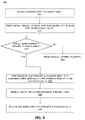
- FIG. 5 is a flow chart of a method 500 for handling a network packet received at an MCN-side interface from the network stack according to various embodiments.
- the method 500 can be performed by processing logic that can include hardware (e.g., processing device, circuitry, dedicated logic, programmable logic, microcode, hardware of a device, integrated circuit, etc.), software (e.g., instructions run or executed on a processing device), or a combination thereof.
- the method 500 is performed by the MCN processor 150 executing the MCN driver 157 , as illustrated in FIG. 1 B , previously referenced as the MCN-side interface.
- the processing logic receives a network packet from the network stack 415 .
- the processing logic reads a transmit start pointer (e.g., tx-start 302 ) and a transmit end pointer (e.g., tx-end 304 ) from the local buffer 180 for the network packet.
- a transmit start pointer e.g., tx-start 302
- a transmit end pointer e.g., tx-end 304
- the processing logic determines whether there is enough space available in the TX buffer 184 (of the local buffer 180 ) for the network packet. If there is not space, at operation 525 , the processing logic reports the local buffer 180 as being busy, e.g., NETDEV_TX_BUSY. If there is sufficient space, at operation 530 , the processing logic writes the packet length 330 followed by the packet data 340 (of the network packet) into the TX buffer 184 , starting at a buffer address to which points the transmit end pointer (tx-end 304 ).
- the processing logic updates a value for the transmit end pointer (tx-end 304 ) in the local buffer.
- the processing logic sets a transmit polling field (tx-poll 306 ) of the local buffer 180 to a non-zero value to indicate that a new packet is enqueued in the TX buffer 184 .
- Memory fences may be used to ensure that the packet data has been copied correctly, prior to setting these control bits.
- FIG. 5 describes the flow of sending a network packet from an MCN node and receiving the network packet at the host processor 122 , since the host and MCN nodes run similar drivers (which was discussed with reference to FIG. 4 ), except for some minor differences, the packet transmission/reception flow is mirrored for the host processor 122 to send a network packet to an MCN node, e.g., the MCN DIMM 146 . Some of these minor differences include that the host node will assert the receive polling field 316 to trigger the hardware interrupt (IRQ) to the core of the MCN processor 150 , as was discussed, so that the MCN processor 150 knows of the incoming (received) data.
- IRQ hardware interrupt
- FIG. 6 is a flow chart of a method 600 for a host-side polling agent to determine whether local buffers of MCN processors are attempting to transmit data according to various embodiments.
- the method 600 can be performed by processing logic that can include hardware (e.g., processing device, circuitry, dedicated logic, programmable logic, microcode, hardware of a device, integrated circuit, etc.), software (e.g., instructions run or executed on a processing device), or a combination thereof.
- the method 600 is performed by the host processor 122 executing the host driver 127 , as illustrated in FIG. 1 A , which may include a host-side polling agent 410 A for example.
- the host-side polling agent may be employed to notify the host processor 122 of incoming packets, which is comparable to functionality of a high-speed NIC.
- the processing logic periodically reads the transmit polling field (tx-poll 306 ) in a plurality of local buffers across a plurality of MCN nodes.
- the processing logic determines whether there is a pending network packet in any of the local buffers. If there is no pending network packet, the method 600 , loops back to operation 610 to continue polling the local buffers for a pending network packet.
- the processing logic reads a transmit start pointer (tx-start 302 ) and a transmit end pointer (tx-end 304 ) from the local buffer 180 for the pending network packet.
- the processing logic reads a cache line at a location of the local buffer 180 to which the transmit start pointer (tx-start 302 ) points.
- the processing logic retrieves the packet length and a packet destination MAC address (e.g., dest-mac) from the cache line. In an Ethernet packet, the first six bytes of the data construct the destination MAC address.
- the processing logic transmits the pending network packet to the packet forwarding engine 406 of the MCN-side interface.
- the processing logic determines whether the transmit start pointer (tx-start 302 ) moved by a number of bytes read from the TX buffer 184 of the local buffer 180 is equal to a value of the transmit end pointer. If the number of bytes the transmit start pointer has moved is not equal to the value of the transmit end pointer, at operation 640 , the processing logic reads another cache line from the local buffer 180 and continues with operations 650 and 660 for the additional cache line. If the number of bytes the transmit start pointer has moved is equal to the value of the transmit end pointer, at operation 680 , reset a value of a transmit polling field of the local buffer and exit.
- FIG. 7 is a flow chart of a method 700 for the host processor 122 to decide where to route a network packet depending on its medium access control (MAC) address according to various embodiments.
- the method 700 can be performed by processing logic that can include hardware (e.g., processing device, circuitry, dedicated logic, programmable logic, microcode, hardware of a device, integrated circuit, etc.), software (e.g., instructions run or executed on a processing device), or a combination thereof.
- the method 700 is performed by the host processor 122 executing the host driver 127 ( FIG. 1 A ).
- the host processor 122 may utilize the packet forwarding engine 406 of the host driver 127 , for example, in execution of the method 700 .
- the processing logic receives a network packet with a destination MAC address (e.g., dest-mac).
- a destination MAC address e.g., dest-mac
- the processing logic determines to which MAC address the destination MAC address matches.
- the processing logic determines that the dest-mac of the incoming network packet matches the MAC address of the host-side interface.
- processing logic determines the dest-mac of the incoming network packet matches a reserved address for broadcast.
- the processing logic allocates a socket buffer.
- the processing logic copies data of the network packet from the receiving (RX) buffer 186 of the local buffer 180 to the socket buffer.
- the processing logic transmits the data from the socket buffer to a network stack for processing.
- the processing logic may perform operations 740 through 760 and additionally, at operation 770 , transmit data from the socket buffer to multiple MCN network nodes (as in broadcasted to available MCN network nodes). This broadcast of the data may be transmitted as described with reference to FIG. 5 .
- the dest-mac of the network packet instead matches an MCN-side interface of a reachable MCN node. If so, at operation, 790 , the processing logic transmit the network packet to the destination MCN node to which the dest-mac matches, e.g., by using the operations discussed with reference to FIG. 5 .
- the memory mapping unit 402 of the MCN driver 157 may function as follows.
- the ioremap() function in Linux
- the ioremap() function by default creates a page mapping that is tagged as uncacheable in the ARMTM architecture.
- the ioremap() function is used to map the physical address of an I/O device to the kernel virtual address.
- the kernel creates a page table, e.g., a mapping of virtual address to the physical address that is requested. When the kernel does an iounmap(), this mapping is destroyed.
- Making the page mapping uncacheable enables the physical address space of the MCN processor 150 to be uncacheable, and thus avoid MCN-processed data from being trapped up in cache of the MCN processor 150 when the data should instead be sent on (either to the host processor 122 or stored into local DRAM). Accordingly, making the page mapping uncacheable may prevent unnecessary delay in data processing. While the memory mapping unit 402 making this page mapping (e.g., the page table) as uncacheable prevents coherency issues, the maximum size of a memory access to an uncacheable memory space is double word (e.g., 64 bits).
- the MCN processor 150 may access memory at cache line granularity. Accessing data at cache line granularity may be done using a memory mapping function, e.g., memremap() with a MEMREMAP_WC flag, which a similar functionality to ioremap() Accessing data at cache line granularity may allow the ability of the MCN MC 170 to perform a write combining, into a group, consecutive write requests (e.g., write commands) at a cache line granularity inside its write queue.
- a memory mapping function e.g., memremap() with a MEMREMAP_WC flag
- the host driver 127 may use an uncacheable memory mapping with the write combining support for the TX buffer 184 and a cacheable memory mapping for the RX buffer 186 .
- the host driver 127 may explicitly invalidate the cache lines in the range of RX buffer after receiving a packet.
- the MCN-side interface is cognizant of the memory channel interleaving performed by the memory subsystem 110 , wherein the successive cache lines in the physical address space are mapped evenly across all the MCs of the host processor 122 . This is to maximize the memory channel parallelism when there is spatial locality between the memory accesses. Without accounting for the memory interleaving, a na ⁇ ve memory copy (e.g., memcpy) would incorrectly spread the packet data across MCN DIMMs in different memory channels, although the host MCs 130 A and 130 B should send the packet data to a particular MCN DIMM's address space.
- a na ⁇ ve memory copy e.g., memcpy
- the host driver 127 may be adapted with a pair of new memory copy functions (e.g., memcpy_to_mcn and memcpy_from_mcn) to map memory operations interleaved across two or more global memory channels 102 A and 102 B of the host processor 122 to the local buffer of multiple memory modules (e.g., MCN DIMMs of FIG. 1 A ).
- the local buffers may be isolated from the two or more global memory channels.
- These new memory copy functions may perform memory copying such that the 64-byte blocks within the address space of the MCN DIMMs are interleaved in a manner that reflects the memory interleaving of the host processor 122 . This allows the MCN driver 157 to send a network packet to an appropriate memory channel and thus an appropriate MCN DIMM.
- FIG. 8 is a set of graphs illustrative of host processor view of interleaved arrangement of physical address space versus MCN processor views of that physical address space according to an embodiment.
- the host processor 122 may view a single physical address space in which data from memory operations (or requests) are interleaved with regard to one of the global memory channels 102 A or 102 B, e.g., a single memory channel. Accordingly, although consecutive memory operations may be accessing consecutive addresses with MCN physical address space, the host processor 122 may still interleave the memory accesses across the global memory channels, as illustrated on left in FIG. 8 , which may be understood to show one of the global memory channels.
- the MCN processor 150 views multiple memory channels depending on a number of the local memory channels 142 existing within the MCN processor 150 . Because consecutive memory accesses to consecutive physical addresses within the MCN physical address space should occur at the same global memory channel 102 A or 102 B, the host driver 127 may be adapted to perform a pair of memory copy functions to map memory operations interleaved across two or more global memory channels of the host processor to a single global memory channel on which the destination MCN DIMM 146 is installed. In other words, the host driver 127 may perform the memory copy functions to map memory operations, which are directed at consecutive addresses of physical memory space of the plurality of memory modules, to a single global memory channel to which is coupled an identified memory module associated with the consecutive addresses.
- the host MC 130 A or 130 B may then direct the mapped memory operations to the single global memory channel.
- the host driver 127 operation may further enable the host processor 122 to broadcast network packets to multiple memory modules (e.g., MCN DIMMs) over a single global memory channel.
- the above-mentioned pair of memory copy functions may include a copy-to-MCN function (e.g., memcpy_to_mcn(mcn_dest, host_src)) and a copy-from-MCN function (e.g., memcpy_from_mcn(host_dest, mcn_src)) in order to appropriately write to and read from consecutive physical memory addresses with respect to the MCN processor view of the address space (on the right in FIG. 8 ).
- a copy-to-MCN function e.g., memcpy_to_mcn(mcn_dest, host_src)
- a copy-from-MCN function e.g., memcpy_from_mcn(host_dest, mcn_src)
- the copy-to-MCN function may cause host_src (or transmission) data (which may be allocated on CONV DIMMs 112 AB or 114 AB and is interleaved between global memory channels 102 A and 102 B) to be copied to an identified MCN memory module over a single global memory channel 102 A or 102 B ( FIG. 1 A ).
- the identified memory module is a destination MCN DIMM 116 A or 116 B (over global memory channel 102 A) or 118 A or 118 B (over global memory channel 102 B).
- the copy-to MCN function performs as a write to the MCN DIMM, and is thus directed at physical address space of the local buffer 180 .
- the host driver 127 may split data packets into chunks, appropriately address these chunks according to the global channel interleaving, and forward the newly addressed data chucks to the host MC 130 A or 130 B.
- the copy-from-MCN function may perform the opposite operation, e.g., is to read mcn_src (or receive) data from the single global memory channel (e.g., from the local buffer 180 of the identified memory module) and write the mcn_src data to a host destination (host_dest) buffer.
- the host_dest buffer may be allocated on CONV DIMMs and be interleaved between the global memory channels 102 A and 102 B.
- these new memory functions may, in this way, map a host processor view of the physical address space to an MCN processor view of the physical address space that involves two memory channels.
- MCN driver 157 assigned to each local memory channel 142 and a typical distributed application sends packets to multiple MCN nodes, the memory requests from these MCN drivers may still concurrently utilize the global and local memory channels.
- TCP congestion control is implemented for slow, long latency network connections and sometimes takes several seconds to reach to the full bandwidth utilization.
- TCP frequently sends ACK messages to the sender.
- Sending and receiving ACK messages consumes both CPU cycles and network bandwidth. Based on evaluation results, sending and receiving ACK messages incurs up to approximately 25% overhead in a TCP connection, which is aligned with previous studies.
- an MCN DIMM can only use a single channel bandwidth and cannot interleave the memory accesses across multiple memory channels. That being said, the maximum theoretical MCN bandwidth is 12.8 GB/s, which is the maximum bandwidth of a single memory channel. Although the bandwidth of each MCN node is limited to the bandwidth of a single memory channel, this bandwidth is far from being a bottleneck as the bandwidth of a single memory channel alone is more than 100 Gbps. Nonetheless, each MCN DIMM can communicate with the host or each other independently, providing aggregate bandwidth proportional to the total number of memory channels in the system.
- the MCN architecture may deploy use of a specialized TCP/IP stack for the MCN processor 150 that resembles a user space TCP stack such as mTCP.
- the MCN network stack 415 may not rely on the conventional TCP/IP stack, and instead may resemble a shared memory communication channel between host and MCN nodes.
- the present disclosure enables the MCN architecture without changes in the software stack and the host processor architecture.
- the MCN architecture may first exploit the features in the OS and conventional processors, and use an efficient polling mechanism to reduce the communication latency between the host processor 122 and the MCN processors 150 .
- the MCN architecture may exploit the fact that the Bit Error Rate (BER) of a memory channel is orders of magnitude lower than that of a network link and thus may bypass the checksum calculation to detect any error in a received packet and adopt a larger frame size for the packets.
- BER Bit Error Rate
- a core (on the host processor 122 ) running a polling function (such as a tasklet or thread) to determine whether network packets (e.g., MCN messages) are available for transmission in the local buffer 180 can neither sleep nor accept a timer to reschedule. Consequently, the polling function can overwhelm the core by continually rescheduling itself.
- the host processor 122 can employ a high-resolution (HR) timer that reschedules a polling function call at a specific time with a nanosecond resolution. Specifically, whenever the HR-timer routine is invoked, the HR timer schedules a tasklet for running the polling function and then exits.
- HR high-resolution
- the host processor 122 may be programmed to schedule a tasklet because the interrupts in the HR timer service routine are disabled and directly calling the polling function can result in missing the interrupts from other devices while doing the polling. Hence, any function called inside an HR timer should be very short (e.g., scheduling a tasklet). Note that a tasklet is interruptible and does not negatively impact a high priority process.
- the network stack 415 inspects a Cyclic Redundancy Check (CRC) value or checksum of a network packet to detect any error before it delivers the network packet to the next network layer. Since the checksum calculation for each packet consumes host and MCN processors cycles, the checksum calculation may limit the maximum bandwidth and the minimum latency. To reduce such an overhead, the network stack 415 may support an interface to offload the checksum calculations to hardware in the NIC. We propose a much simpler mechanism to efficiently handle checksum calculations. Since a memory channel is protected by ECC-based error detection and correction (and CRC in DDR4), the network stack 415 need not redundantly generate a checksum value for an MCN message. Therefore, the header checksum checking in the TCP/IP network stack 415 may be disabled without affecting the reliability of TCP.
- CRC Cyclic Redundancy Check
- the standard MTU of an Ethernet frame is 1.5 KB, as discussed above.
- a larger MTU can better amortize the protocol processing software overhead and improve the network performance.
- the network stack 415 can support a larger MTU, if the network stack 415 uses the default size as a larger packet going through the conventional Ethernet links, the larger packet is more likely to be corrupted and incur a higher cost for a re-transmission.
- the MCN architecture can efficiently deploy a larger frame size as the BER of a memory channel is typically multiple orders of magnitude lower than that of an Ethernet link. Exploiting such an advantage, the size of the MTU employed within the MCN architecture may be increased, e.g., up to at least 9 KB. This can be done by configuring the interface via the Linux ifconfig utility.
- the unique MCN message format described with reference to FIG. 3 B may seamlessly support any MTU size.
- the network stack 415 may still need to divide a bulk user data chunk into multiple MTU-sized packets. Each of these packets undergoes TCP/IP processing and pays the overhead of segmentation.
- TSO TCP segmentation offload
- the driver of a TSO-enabled NIC provides a TCP/IP header along with a large data chunk to the NIC.
- the TSO-enabled NIC may perform the following actions to send the data chunk. First, the TSO-enabled NIC may divide the data chunk into several MTU sized segments.
- the TSO-enabled NIC may copy the TCP/IP header at the beginning of each data segment.
- the TSO-enabled NIC may calculate and set the Total Length, Header Checksum, and Sequence Number fields of each TCP/IP header.
- the TSO-enabled NIC may send out each MTU sized packet.
- the MCN drivers may support TSO by ensuring that there is sufficient space in the TX and RX buffers 184 , 186 for the largest possible user data chunk allowed by the network stack. Since the network stack 415 can also bypass the performing the checksum, the network stack 415 may also be updated to set the Total Length field of the TCP/IP header to the user data chunk size and then transmit the unsegmented packet to the destination MCN node.
- a high-resolution (HR) timer may be implemented within the polling agent 410 A to more efficiently implement the polling agent 410 A.
- HR-timer an interrupt is asserted, which incurs a performance overhead if the polling fails and no packet is received. If the timer interval is increased to minimize the overhead, then the average packet transmission latency increases as well.
- the driver scans across the MCN DIMMs on all channels, which further increases the overhead of the polling.
- the MCN-DIMMs may leverage an existing hardware interrupt-like signal (e.g., ALERT_N in the DDR4 standard, or other similar signal that can be repurposed) that may be sent to the host MC 130 A or 130 B. More specifically, the host protocol interface 160 may transmit the hardware interrupt-like signal as a hardware interrupt to the host MC 130 A or 130 B, to notify the MC 130 A or 130 B of data available in the local buffer 180 . The host MC receiving the hardware interrupt (e.g., the ALERT_N signal) from a memory channel may then identify (e.g., via polling the local buffers 180 ) which DIMM on the channel has asserted the hardware interrupt.
- ALERT_N in the DDR4 standard, or other similar signal that can be repurposed
- the MC 130 A or 130 B may then relay the signal to a core of the host processor 122 as an interrupt, e.g., as an alert that data is stored in an identified local buffer 180 for transmission to the host MC.
- This mechanism not only eliminates the need for periodic polling, but also allows the MCN driver(s) to immediately know which local memory channel should be checked.
- the host processor 122 and MCN processor 150 may each be responsible for copying packets between local buffers and the MCN physical memory space with the memcpy function. Consequently, the host and MCN processors issuing many memory requests can become a bottleneck, especially when they exchange many packets.
- the host processor 122 may also be responsible for routing packets between MCN nodes, potentially creating another bottleneck when there is a spike in the traffic between MCN nodes.
- MCN DMA engines MCN DMA engines
- MC memory controller
- the MCN-DMA performs the memory copy operations on behalf of the host and MCN processors, and frees up processor cycles for other tasks. Except the fact that an MCN-DMA is to be cognizant of the memory channel interleaving, the MCN-DMA operates similar to a conventional DMA engines in an I/O device.
- FIG. 9 A and FIG. 9 B respectively.
- the prototype MCN DIMM couples two 32 GB DDR3-1066 DIMMs with an Intel (Altera) Stratix V FPGA that interfaces directly with the host memory channel, the IBM Differential Memory Interface (DMI).
- DMI IBM Differential Memory Interface
- NIOS II embedded processor acting as an MCN processor in the FPGA.
- FIG. 9 C depicts the prototype system architecture.
- FIG. 10 illustrates an example machine of a computer system 1000 within which a set of instructions, for causing the machine to perform any one or more of the methodologies discussed herein, can be executed.
- the computer system 1000 can correspond to a host system (e.g., the host system 120 of FIG. 1 ) that includes, is coupled to, or utilizes a memory sub-system (e.g., the memory sub-system 110 of FIG. 1 A ) or can be used to perform the operations of a host MC 130 A or 130 B, the host OS 125 , or the host driver 127 .
- the computer system 1000 can correspond to an MCN module (e.g., DIMM) of FIG. 1 B that includes or is coupled to the MCN MC 170 ( FIG.
- MCN module e.g., DIMM
- the machine can be connected (e.g., networked) to other machines in a LAN, an intranet, an extranet, and/or the Internet.
- the machine can operate in the capacity of a server or a client machine in client-server network environment, as a peer machine in a peer-to-peer (or distributed) network environment, or as a server or a client machine in a cloud computing infrastructure or environment.
- the machine can be a personal computer (PC), a tablet PC, a set-top box (STB), a Personal Digital Assistant (PDA), a cellular telephone, a web appliance, a server, a network router, a switch or bridge, or any machine capable of executing a set of instructions (sequential or otherwise) that specify actions to be taken by that machine.
- PC personal computer
- PDA Personal Digital Assistant
- STB set-top box
- STB set-top box
- a cellular telephone a web appliance
- server a server
- network router a network router
- switch or bridge or any machine capable of executing a set of instructions (sequential or otherwise) that specify actions to be taken by that machine.
- machine shall also be taken to include any collection of machines that individually or jointly execute a set (or multiple sets) of instructions to perform any one or more of the methodologies discussed herein.
- the example computer system 1000 includes a processing device 1002 , a main memory 1004 (e.g., read-only memory (ROM), flash memory, dynamic random access memory (DRAM) such as synchronous DRAM (SDRAM) or Rambus DRAM (RDRAM), etc.), a static memory 1006 (e.g., flash memory, static random access memory (SRAM), etc.), and a data storage system 1018 , which communicate with each other via a bus 1030 .
- main memory 1004 e.g., read-only memory (ROM), flash memory, dynamic random access memory (DRAM) such as synchronous DRAM (SDRAM) or Rambus DRAM (RDRAM), etc.
- DRAM dynamic random access memory
- SDRAM synchronous DRAM
- RDRAM Rambus DRAM
- static memory 1006 e.g., flash memory, static random access memory (SRAM), etc.
- SRAM static random access memory
- Processing device 1002 represents one or more general-purpose processing devices such as a microprocessor, a central processing unit, or the like. More particularly, the processing device can be a complex instruction set computing (CISC) microprocessor, reduced instruction set computing (RISC) microprocessor, very long instruction word (VLIW) microprocessor, or a processor implementing other instruction sets, or processors implementing a combination of instruction sets. Processing device 1002 can also be one or more special-purpose processing devices such as an application specific integrated circuit (ASIC), a field programmable gate array (FPGA), a digital signal processor (DSP), network processor, or the like. The processing device 1002 is configured to execute instructions 1026 for performing the operations and steps discussed herein.
- the computer system 1000 can further include a network interface device 1008 to communicate over the network 1020 .
- the data storage system 1018 can include a machine-readable storage medium 1024 (also known as a computer-readable medium) on which is stored one or more sets of instructions 1026 or software embodying any one or more of the methodologies or functions described herein.
- the instructions 1026 can also reside, completely or at least partially, within the main memory 1004 and/or within the processing device 1002 during execution thereof by the computer system 1000 , the main memory 1004 and the processing device 1002 also constituting machine-readable storage media.
- the machine-readable storage medium 1024 , data storage system 1018 , and/or main memory 1004 can correspond to the memory sub-system 110 of FIG. 1 A or the MCN processor 150 of FIG. 1 C .
- the instructions 1026 include instructions to implement functionality corresponding to any OS, driver, software, or network stacked described herein. While the machine-readable storage medium 1024 is shown in an example embodiment to be a single medium, the term “machine-readable storage medium” should be taken to include a single medium or multiple media that store the one or more sets of instructions. The term “machine-readable storage medium” shall also be taken to include any medium that is capable of storing or encoding a set of instructions for execution by the machine and that cause the machine to perform any one or more of the methodologies of the present disclosure. The term “machine-readable storage medium” shall accordingly be taken to include, but not be limited to, solid-state memories, optical media, and magnetic media.
- the present disclosure also relates to an apparatus for performing the operations herein.
- This apparatus can be specially constructed for the intended purposes, or it can include a general purpose computer selectively activated or reconfigured by a computer program stored in the computer.
- a computer program can be stored in a computer readable storage medium, such as, but not limited to, any type of disk including floppy disks, optical disks, CD-ROMs, and magnetic-optical disks, read-only memories (ROMs), random access memories (RAMs), EPROMs, EEPROMs, magnetic or optical cards, or any type of media suitable for storing electronic instructions, each coupled to a computer system bus.
- the present disclosure can be provided as a computer program product, or software, that can include a machine-readable medium having stored thereon instructions, which can be used to program a computer system (or other electronic devices) to perform a process according to the present disclosure.
- a machine-readable medium includes any mechanism for storing information in a form readable by a machine (e.g., a computer).
- a machine-readable (e.g., computer-readable) medium includes a machine (e.g., a computer) readable storage medium such as a read only memory (“ROM”), random access memory (“RAM”), magnetic disk storage media, optical storage media, flash memory components, etc.
Landscapes
- Engineering & Computer Science (AREA)
- Theoretical Computer Science (AREA)
- General Engineering & Computer Science (AREA)
- Physics & Mathematics (AREA)
- General Physics & Mathematics (AREA)
- Computer Hardware Design (AREA)
- Data Exchanges In Wide-Area Networks (AREA)
Abstract
Description
Claims (8)
Priority Applications (1)
| Application Number | Priority Date | Filing Date | Title |
|---|---|---|---|
| US17/250,785 US11520724B2 (en) | 2018-09-07 | 2019-09-06 | Application-transparent near-memory processing architecture with memory channel network |
Applications Claiming Priority (3)
| Application Number | Priority Date | Filing Date | Title |
|---|---|---|---|
| US201862728416P | 2018-09-07 | 2018-09-07 | |
| PCT/US2019/050027 WO2020051505A1 (en) | 2018-09-07 | 2019-09-06 | Application-transparent near-memory processing architecture with memory channel network |
| US17/250,785 US11520724B2 (en) | 2018-09-07 | 2019-09-06 | Application-transparent near-memory processing architecture with memory channel network |
Related Parent Applications (1)
| Application Number | Title | Priority Date | Filing Date |
|---|---|---|---|
| PCT/US2019/050027 A-371-Of-International WO2020051505A1 (en) | 2018-09-07 | 2019-09-06 | Application-transparent near-memory processing architecture with memory channel network |
Related Child Applications (1)
| Application Number | Title | Priority Date | Filing Date |
|---|---|---|---|
| US17/980,685 Division US12210473B2 (en) | 2018-09-07 | 2022-11-04 | Application-transparent near-memory processing architecture with memory channel network |
Publications (2)
| Publication Number | Publication Date |
|---|---|
| US20210209047A1 US20210209047A1 (en) | 2021-07-08 |
| US11520724B2 true US11520724B2 (en) | 2022-12-06 |
Family
ID=69722753
Family Applications (2)
| Application Number | Title | Priority Date | Filing Date |
|---|---|---|---|
| US17/250,785 Active US11520724B2 (en) | 2018-09-07 | 2019-09-06 | Application-transparent near-memory processing architecture with memory channel network |
| US17/980,685 Active 2039-10-23 US12210473B2 (en) | 2018-09-07 | 2022-11-04 | Application-transparent near-memory processing architecture with memory channel network |
Family Applications After (1)
| Application Number | Title | Priority Date | Filing Date |
|---|---|---|---|
| US17/980,685 Active 2039-10-23 US12210473B2 (en) | 2018-09-07 | 2022-11-04 | Application-transparent near-memory processing architecture with memory channel network |
Country Status (2)
| Country | Link |
|---|---|
| US (2) | US11520724B2 (en) |
| WO (1) | WO2020051505A1 (en) |
Cited By (1)
| Publication number | Priority date | Publication date | Assignee | Title |
|---|---|---|---|---|
| US20230071386A1 (en) * | 2018-09-07 | 2023-03-09 | The Board Of Trustees Of The University Of Illinois | Application-transparent near-memory processing architecture with memory channel network |
Families Citing this family (8)
| Publication number | Priority date | Publication date | Assignee | Title |
|---|---|---|---|---|
| EP4675992A3 (en) * | 2019-12-23 | 2026-04-15 | NTT, Inc. | Intra-server delay control device, intra-server delay control method, and program |
| JP7485101B2 (en) * | 2021-02-10 | 2024-05-16 | 日本電信電話株式会社 | Intra-server delay control device, intra-server delay control method and program |
| US12028276B2 (en) | 2021-08-24 | 2024-07-02 | International Business Machines Corporation | Transport control word architecture for virtual port mirroring |
| US11722436B2 (en) * | 2021-08-24 | 2023-08-08 | International Business Machines Corporation | Transport control word architecture for physical port mirroring |
| US12094525B2 (en) | 2022-07-22 | 2024-09-17 | International Business Machines Corporation | Multichannel memory to augment local memory |
| WO2024205571A1 (en) * | 2023-03-28 | 2024-10-03 | Zeku, Inc. | System and method for near-memory computing with uncacheable memory units |
| US20260037454A1 (en) * | 2024-08-01 | 2026-02-05 | SK Hynix NAND Product Solutions Corp. (dba Solidigm) | Communication between a computing element of a memory device and an electronic device |
| CN119484276B (en) * | 2025-01-08 | 2025-04-15 | 龙芯中科技术股份有限公司 | Ethernet card initialization processing method, device, equipment and storage medium |
Citations (13)
| Publication number | Priority date | Publication date | Assignee | Title |
|---|---|---|---|---|
| US5243596A (en) * | 1992-03-18 | 1993-09-07 | Fischer & Porter Company | Network architecture suitable for multicasting and resource locking |
| US5819051A (en) * | 1995-12-29 | 1998-10-06 | Compaq Computer Corporation | Low speed serial bus protocol and circuitry |
| US5903718A (en) * | 1996-09-16 | 1999-05-11 | International Business Machines Corporation | Remote program monitor method and system using a system-under-test microcontroller for self-debug |
| US20040081005A1 (en) | 1999-07-23 | 2004-04-29 | Rambus Inc. | Memory system with channel multiplexing of multiple memory devices |
| US20070008989A1 (en) * | 2005-06-30 | 2007-01-11 | Intel Corporation | Packet processing |
| US20100005219A1 (en) * | 2008-07-01 | 2010-01-07 | International Business Machines Corporation | 276-pin buffered memory module with enhanced memory system interconnect and features |
| US20110047302A1 (en) * | 1992-07-02 | 2011-02-24 | U.S. Ethernet Innovations | Programmed i/o ethernet adapter with early interrupts for accelerating data transfer |
| US20130100963A1 (en) * | 2011-10-24 | 2013-04-25 | Richard L. Hartman | Methods, Systems, and Devices for Interfacing to Networks |
| US20160055021A1 (en) | 2014-08-23 | 2016-02-25 | Vmware, Inc. | Rapid suspend/resume for virtual machines via resource sharing |
| US20160162404A1 (en) * | 2013-07-27 | 2016-06-09 | Netlist, Inc. | Memory module with local synchronization |
| US20160364347A1 (en) * | 2015-06-09 | 2016-12-15 | Rambus Inc. | Memory system design using buffer(s) on a mother board |
| US20180239725A1 (en) | 2017-02-17 | 2018-08-23 | Intel Corporation | Persistent Remote Direct Memory Access |
| US10191865B1 (en) * | 2016-04-14 | 2019-01-29 | Amazon Technologies, Inc. | Consolidating write transactions for a network device |
Family Cites Families (20)
| Publication number | Priority date | Publication date | Assignee | Title |
|---|---|---|---|---|
| US6981034B2 (en) * | 1999-06-30 | 2005-12-27 | Nortel Networks Limited | Decentralized management architecture for a modular communication system |
| US20030130832A1 (en) * | 2002-01-04 | 2003-07-10 | Peter Schulter | Virtual networking system and method in a processing system |
| TWI227616B (en) * | 2001-11-20 | 2005-02-01 | Hitachi Ltd | Packet communication device, packet communication system, packet communication module, data processor and data transmission system |
| US6987961B1 (en) * | 2004-06-28 | 2006-01-17 | Neomagic Corp. | Ethernet emulation using a shared mailbox between two processors in a feature phone |
| US8239594B2 (en) * | 2005-11-10 | 2012-08-07 | Datacard Corporation | Modular card issuance system and method of operation |
| US7620526B2 (en) * | 2006-10-25 | 2009-11-17 | Zeugma Systems Inc. | Technique for accessing a database of serializable objects using field values corresponding to fields of an object marked with the same index value |
| US7941613B2 (en) * | 2007-05-31 | 2011-05-10 | Broadcom Corporation | Shared memory architecture |
| WO2009065313A1 (en) * | 2007-11-20 | 2009-05-28 | Hangzhou H3C Technologies Co., Ltd. | Method and multi-core processor equipment for realizing multiple service process functions |
| US8249101B2 (en) * | 2010-03-26 | 2012-08-21 | Raytheon Company | Mobile ad hoc network configured as a virtual internet protocol network |
| US20120151048A1 (en) * | 2010-12-10 | 2012-06-14 | Kazuki Kitazawa | Communication device, apparatus, system, and method of setting communication device, and communication device setting program |
| KR20120139129A (en) * | 2011-06-16 | 2012-12-27 | 삼성전자주식회사 | Apparatus for and method of accessing network memory |
| US9189264B1 (en) * | 2014-06-09 | 2015-11-17 | Western Digital Technologies, Inc. | Notification propagation in virtual computing environment |
| US10168997B2 (en) * | 2014-06-26 | 2019-01-01 | Ngd Systems, Inc. | System and method for executing native client code in a storage device |
| US9977762B2 (en) * | 2015-04-22 | 2018-05-22 | International Microsystems, Inc. | Disjoint array computer |
| US10860511B1 (en) * | 2015-12-28 | 2020-12-08 | Western Digital Technologies, Inc. | Integrated network-attachable controller that interconnects a solid-state drive with a remote server computer |
| US10599600B2 (en) * | 2017-06-16 | 2020-03-24 | Western Digital Technologies, Inc. | Peripheral Component Interconnect Express (PCIe) switching for multi-host computing system deployments |
| US10798059B1 (en) * | 2017-10-06 | 2020-10-06 | Juniper Networks, Inc | Apparatus, system, and method for applying firewall rules at dynamic offsets within packets in kernel space |
| US10691544B2 (en) * | 2017-11-21 | 2020-06-23 | International Business Machines Corporation | Modifying a container instance network |
| US10671134B2 (en) * | 2018-01-10 | 2020-06-02 | International Business Machines Corporation | Memory modules with secondary, independently powered network access path |
| US11520724B2 (en) * | 2018-09-07 | 2022-12-06 | The Board Of Trustees Of The University Of Illinois | Application-transparent near-memory processing architecture with memory channel network |
-
2019
- 2019-09-06 US US17/250,785 patent/US11520724B2/en active Active
- 2019-09-06 WO PCT/US2019/050027 patent/WO2020051505A1/en not_active Ceased
-
2022
- 2022-11-04 US US17/980,685 patent/US12210473B2/en active Active
Patent Citations (13)
| Publication number | Priority date | Publication date | Assignee | Title |
|---|---|---|---|---|
| US5243596A (en) * | 1992-03-18 | 1993-09-07 | Fischer & Porter Company | Network architecture suitable for multicasting and resource locking |
| US20110047302A1 (en) * | 1992-07-02 | 2011-02-24 | U.S. Ethernet Innovations | Programmed i/o ethernet adapter with early interrupts for accelerating data transfer |
| US5819051A (en) * | 1995-12-29 | 1998-10-06 | Compaq Computer Corporation | Low speed serial bus protocol and circuitry |
| US5903718A (en) * | 1996-09-16 | 1999-05-11 | International Business Machines Corporation | Remote program monitor method and system using a system-under-test microcontroller for self-debug |
| US20040081005A1 (en) | 1999-07-23 | 2004-04-29 | Rambus Inc. | Memory system with channel multiplexing of multiple memory devices |
| US20070008989A1 (en) * | 2005-06-30 | 2007-01-11 | Intel Corporation | Packet processing |
| US20100005219A1 (en) * | 2008-07-01 | 2010-01-07 | International Business Machines Corporation | 276-pin buffered memory module with enhanced memory system interconnect and features |
| US20130100963A1 (en) * | 2011-10-24 | 2013-04-25 | Richard L. Hartman | Methods, Systems, and Devices for Interfacing to Networks |
| US20160162404A1 (en) * | 2013-07-27 | 2016-06-09 | Netlist, Inc. | Memory module with local synchronization |
| US20160055021A1 (en) | 2014-08-23 | 2016-02-25 | Vmware, Inc. | Rapid suspend/resume for virtual machines via resource sharing |
| US20160364347A1 (en) * | 2015-06-09 | 2016-12-15 | Rambus Inc. | Memory system design using buffer(s) on a mother board |
| US10191865B1 (en) * | 2016-04-14 | 2019-01-29 | Amazon Technologies, Inc. | Consolidating write transactions for a network device |
| US20180239725A1 (en) | 2017-02-17 | 2018-08-23 | Intel Corporation | Persistent Remote Direct Memory Access |
Non-Patent Citations (65)
| Title |
|---|
| "Coral Benchmark Codes," available at https://asc.llnl.gov/CORAL-benchmarks/, 8 pages. |
| "Ethernet frame" available at https://en.wikipedia.org/wiki/Ethernet frame, accessed: Mar. 25, 2018, 8 pages. |
| "IPERF: The ultimate speed test tool for TCP, UDP and SCTP," available at https://iperf.fr/, 3 pages. |
| "IPv4 standard," https://en.wikipedia.org/wiki/IPv4, accessed: Mar. 25, 2018, 9 pages. |
| "TCP frame," available at https://en.wikipedia.org/wiki/Transmission Control Protocol, accessed: Mar. 25, 2018, 14 pages. |
| Ahn et al., "A scalable processing-in-memory accelerator for parallel graph processing" ACM/IEEE International Symposium on Computer Architecture (ISCA), Jun. 2015, 13 pages. |
| Ahn et al., "PIM-enabled instructions: A low-overhead, locality-aware processing-in-memory architecture," in Computer Architecture (ISCA), 2015 ACM/IEEE 42nd Annual International Symposium on. IEEE, 2015, 13 pages. |
| Alian et al., "Dist-gem5: Distributed Simulation of Computer Clusters," in ISPASS, 2017, 29 pages. |
| Anderson, et al., "Overcoming the Internet impasse through Virtualization," Computer, vol. 38, 2005, 7 pages. |
| Andreyev, Alexey, "Introducing data center fabric, the next-generation Facebook data center network," 2014, available at https://code.facebook.com/posts/360346274145943/, 11 pages. |
| Asghari-Moghaddam, et al., "Chameleon: Versatile and Practical Near-DRAM Acceleration Architecture for Large Memory Systems," MICRO, 2016, 13 pages. |
| Asghari-Moghaddam, et al., "Near-DRAM acceleration with single-ISA heterogeneous processing in standard memory modules," IEEE Micro, vol. 36, 2016, 11 pages. |
| Awan et al., "Identifying the potential of near data processing for apache spark," Proceedings of the International Symposium on Memory Systems. ACM, 2017, 8 pages. |
| Bailey et al., "The NAS parallel benchmarks," The International Journal of Supercomputing Applications, vol. 5, 1991, 13 pages. |
| Bridges et al., "Users Guide to MPICH, a Portable Implementation of MPI," Argonne National Laboratory, vol. 9700, 1995, 35 pages. |
| Chan et al., "Improving server application performance via pure TCP ACK receive optimization," Presented as part of the 2013 USENIX Annual Technical Conference (USENIX ATC 13), San Jose, CA: USENIX, 2013, available at https://www.usenix.org/conference/atc13/technical-sessions/presentation/chan, 6 pages. |
| Chu et al, "Highlevel Programming Model Abstractions for Processing in Memory," Workshop on Near-Data Processing, Dec. 2013, 4 pages. |
| Connery et al., "Offload of tcp segmentation to a smart adapter," Aug. 10, 1999, U.S. Pat. No. 5,937,169, 19 pages. |
| Deering et al., "FBRAM: a New Form of Memory Optimized for 3D Graphics," SIGGRAPH, Jul. 1994, 8 pages. |
| Draper, et al., "The Architecture of the DIVA Processing-in-memory Chip," ICS, Jun. 2002, 12 pages. |
| Dumazet, Eric, "Busy polling: Past, present, future," NetDev 2.1, 2017, 4 pages. |
| Elliot et al., "Computational RAM: A Memory-SIMD Hybrid and its Application to DSP," CICC, May 1992, 6 pages. |
| Farmahini-Farahani et al., "NDA: Near-DRAM Acceleration Architecture Leveraging Commodity DRAM Devices and Standard Memory Modules," in HPCA, Feb. 2015, 13 pages. |
| Gao et al., "Practical near-data processing for in-memory analytics frameworks," Parallel Architecture and Compilation (PACT), 2015 International Conference on. IEEE, 2015, 12 pages. |
| Grossman, Leonid, "Large receive offload implementation in neterion 10gbe ethemet driver," Linux Symposium, 2005, 6 pages. |
| Gutierrez et al., "Integrated 3D-stacked server designs for increasing physical density of key-value stores," in 19th International Conference on Architectural Support for Programming Languages and Operating Systems, ASPLOS 2014, 14 pages. |
| Intel, "An Introduction to the Intel R QuickPath Interconnect," Document No. 320412-001US, Jan. 2009, https://www.intel.com/content/dam/doc/white-paper/quick-path-interconnect-introduction-paper.pdf, 22 pages. |
| Intel, "Avalon R Interface Specifications," available at https://www.altera.com/content/dam/altera-www/global/en_US/pdfs/literature/manual/mnl_avalon_spec.pdf, 2017, 70 pages. |
| Intel, "IvyTown Xeon + FPGA: The HARP Program," Workshop: CPU+FPGA—OpenCL Based High Level Synthesis for CPU+FPGA Coherent Systems, International Symposium on Computer Architecture, ISCA, 2016, https://cpufpga.files.wordpress.com/2016/04/harp_isca_2016_final.pdf, 34 pages. |
| Intel, "Nios II Processor," available at https://www.altera.com/products/processors/overview.html, 2017, 11 pages. |
| International Search Report and Written Opinion for International Application No. PCT/US2019/050027, 13 pages, dated Nov. 25, 2019. |
| Jacob et al, "Virtual memory in contemporary microprocessors," IEEE Micro, vol. 18, 1998, 17 pages. |
| Jeong, et al., "mTCP: A Highly Scalable User-level TCP Stack for Multicore Systems," Proceedings of the 11th USENIX Conference on Networked Systems Design and Implementation, serial NSDI'14, Berkeley, CA, USA: USENIX Association, 2014, 15 pages. |
| Kang et al., "FlexRAM: Toward an Advanced Intelligent Memory System," ICCD, Oct. 1999, 10 pages. |
| Kersey et al., "Lightweight simt core designs for intelligent 3d stacked dram," Proceedings of the International Symposium on Memory Systems. ACM, 2017, 11 pages. |
| Li et al., "McPAT: An Integrated Power, Area, and Timing Modeling Framework for Multicore and Manycore Architectures" in MICRO, 2009, 12 pages. |
| Lloyd et al., 8. S. Lloyd and M. Gokhale, "Near memory key/value lookup acceleration," Proceedings of the International Symposium on Memory Systems. ACM, 2017, 8 pages. |
| Loh, Gabriel H., "3D-Stacked Memory Architectures for Multi-core Processors," ISCA, Jun. 2008, 14 pages. |
| Mai et al., "Smart Memories: A Modular Reconfigurable Architecture," ISCA, Jun. 2000, 11 pages. |
| Meany et al., "The IBM z13 memory subsystem for big data," IBM Journal of Research and Development, vol. 59, Jul. 2015, 11 pages. |
| Melzer, et al., "IP checksum offload," Apr. 27, 1999, U.S. Pat. No. 5,898,713, 11 pages. |
| Micron, "3D XPointTM Technology," https://www.micron.com/products/advanced-solutions/3d-xpoint-technology, Oct. 24, 2019, 1 page. |
| Micron, "NVDIMM," 2016, available at https://www.micron.com/products/dram-modules/nvdimm/, 2 pages. |
| Nai et al., "Graphpim: Enabling instruction-level pim offloading in graph computing frameworks," High Performance Computer Architecture (HPCA), 2017 IEEE International Symposium on. IEEE, 2017, 12 pages. |
| Nair et al., "Active memory cube: A processing-in-memory architecture for exascale systems," IBM Journal of Research and Development, vol. 59, 2015,14 pages. |
| Nvidia, "Nvidia R TegraR X1," https://international.download.nvidia.com/pdf/tegra/Tegra-X1-whitepaper-v1.0.pdf, 2015, 41 pages. |
| Oskin et al., "Active Pages: A Computation Model for Intelligent Memory," ISCA, Jun. 1998, 12 pages. |
| Patterson et al., "A Case for Intelligent RAM," Micro, IEEE, vol. 17, Mar. 1997, 11 pages. |
| Patterson et al., "Intelligent RAM (IRAM): the industrial setting, applications, and architectures," ICCD, Oct. 1997, 2 pages. |
| Pawlowski, J. Thomas, "Hybrid Memory Cube," Hot Chips, Aug. 2011, 24 pages. |
| Pugsley et al., "Comparing Implementations of Near-Data Computing with In-Memory MapReduce Workloads," Micro, IEEE, vol. 34, Jul. 2014, 9 pages. |
| Pugsley et al., "NDC: Analyzing the impact of 3D-stacked memory+ logic devices on MapReduce workloads," Performance Analysis of Systems and Software (ISPASS), 2014 IEEE International Symposium on. IEEE, 2014, 11 pages. |
| Qualcomm, "Snapdragon 835 Mobile Platform," 2016. [Online]. Available: https://www.qualcomm.com/products/snapdragon/processors/835, 9 pages. |
| Seshadri et al., "Ambit: In-memory accelerator for bulk bitwise operations using commodity dram technology," in Proceedings of the 50th Annual IEEE/ACM International Symposium on Microarchitecture. ACM, 2017, 15 pages. |
| Shvachko et al., "The hadoop distributed file system," Mass storage systems and technologies (MSST), 2010 IEEE 26th symposium on. IEEE, 2010, 20 pages. |
| Singh et al., "Jupiter rising: A decade of close topologies and centralized control in Google's datacenter network," Sigcomm '15, 2015, 15 pages. |
| Stuecheli et al., "CAPI: A Coherent Accelerator Processor Interface," IBM Journal of Research and Development, vol. 59, Jan. 2015, 7 pages. |
| Sukhwani et al., "Contutto: A Novel FPGA-based Prototyping Platform Enabling Innovation in the Memory Subsystem of a Server Class Processor," in Proceedings of the 50th Annual IEEE/ACM International Symposium on Microarchitecture, ser. MICRO-50 '17, 2017, 12 pages. |
| The Tech Report, "The Exynos 5433 SoC,," Jan. 31, 2015, http://techreport.com/review/27539/samsung-galaxy-note-4-with-the-exynos-5433-processor/2, 59 pages. |
| Turner et al., "Diversifying the Internet," in Global Telecommunications Conference, 2005, GLOBECOM'05. IEEE, vol. 2. IEEE, 2005, 6 pages. |
| Wang et al., "Bigdatabench: A big data benchmark suite from internet services," High Performance Computer Architecture (HPCA), 2014 IEEE 20th International Symposium on. IEEE, 2014, 12 pages. |
| Wei, Andy, "Qualcomm snapdragon 835 first to 10 nm," http://www.techinsights.com/about-techinsights/overview/blog/qualcomm-snapdragon-835-first-to-10-nm/, 2017, 2 pages. |
| Zaharia et al., "Spark: Cluster computing with working sets," Proceedings of the 2nd USENIX Conference on Hot Topics in Cloud Computing, ser. HotCloud'10. Berkeley, CA, USA: USENIX Association, 2010, 7 pages. |
| Zhang et al.,"TOP-PIM: throughput-oriented programmable processing in memory," in Proceedings of the 23rd international symposium on High-performance parallel and distributed computing. ACM, 2014, 14 pages. |
| Zhu et al., "A 3D-stacked Logic-in-memory Accelerator for Application-Specific Data Intensive Computing," 3DIC, Oct. 2013, 7 pages. |
Cited By (2)
| Publication number | Priority date | Publication date | Assignee | Title |
|---|---|---|---|---|
| US20230071386A1 (en) * | 2018-09-07 | 2023-03-09 | The Board Of Trustees Of The University Of Illinois | Application-transparent near-memory processing architecture with memory channel network |
| US12210473B2 (en) * | 2018-09-07 | 2025-01-28 | The Board Of Trustees Of The University Of Illinois | Application-transparent near-memory processing architecture with memory channel network |
Also Published As
| Publication number | Publication date |
|---|---|
| US12210473B2 (en) | 2025-01-28 |
| US20230071386A1 (en) | 2023-03-09 |
| WO2020051505A1 (en) | 2020-03-12 |
| US20210209047A1 (en) | 2021-07-08 |
Similar Documents
| Publication | Publication Date | Title |
|---|---|---|
| US12210473B2 (en) | Application-transparent near-memory processing architecture with memory channel network | |
| Alian et al. | Application-transparent near-memory processing architecture with memory channel network | |
| US12386751B2 (en) | Composable infrastructure enabled by heterogeneous architecture, delivered by CXL based cached switch SOC and extensible via cxloverethernet (COE) protocols | |
| EP3916566B1 (en) | System and method for managing memory resources | |
| US12572491B2 (en) | Memory with cache-coherent interconnect | |
| US10877695B2 (en) | Memcached server functionality in a cluster of data processing nodes | |
| US10140245B2 (en) | Memcached server functionality in a cluster of data processing nodes | |
| US10135731B2 (en) | Remote memory access functionality in a cluster of data processing nodes | |
| US9648102B1 (en) | Memcached server functionality in a cluster of data processing nodes | |
| US11693809B2 (en) | Asymmetric read / write architecture for enhanced throughput and reduced latency | |
| US7558887B2 (en) | Method for supporting partial cache line read and write operations to a memory module to reduce read and write data traffic on a memory channel | |
| US7861014B2 (en) | System for supporting partial cache line read operations to a memory module to reduce read data traffic on a memory channel | |
| US11720290B2 (en) | Memcached server functionality in a cluster of data processing nodes | |
| US20090063730A1 (en) | System for Supporting Partial Cache Line Write Operations to a Memory Module to Reduce Write Data Traffic on a Memory Channel | |
| US10346342B1 (en) | Uniform memory access architecture | |
| CN114138707B (en) | A Data Transmission System Based on FPGA | |
| CN119046211B (en) | Data processing system, method and computer system | |
| US20250199980A1 (en) | Translating Between CXL.mem and CXL.cache Read Transactions | |
| US11487695B1 (en) | Scalable peer to peer data routing for servers | |
| Kim et al. | Network interface data caching | |
| Nan et al. | Plug & Offload: Transparently Offloading TCP Stack onto Off-path SmartNIC with PnO-TCP | |
| US20250156100A1 (en) | Fine-grained data mover | |
| Liang et al. | Self-adaptive and Topology-aware Broadcast Leveraging Collective Offload on Tianhe Express Interconnect |
Legal Events
| Date | Code | Title | Description |
|---|---|---|---|
| AS | Assignment |
Owner name: THE BOARD OF TRUSTEES OF THE UNIVERSITY OF ILLINOIS, ILLINOIS Free format text: ASSIGNMENT OF ASSIGNORS INTEREST;ASSIGNORS:KIM, NAM SUNG;ALIAN, MOHAMMAD;SIGNING DATES FROM 20190911 TO 20200622;REEL/FRAME:055488/0652 |
|
| FEPP | Fee payment procedure |
Free format text: ENTITY STATUS SET TO UNDISCOUNTED (ORIGINAL EVENT CODE: BIG.); ENTITY STATUS OF PATENT OWNER: SMALL ENTITY |
|
| FEPP | Fee payment procedure |
Free format text: ENTITY STATUS SET TO SMALL (ORIGINAL EVENT CODE: SMAL); ENTITY STATUS OF PATENT OWNER: SMALL ENTITY |
|
| STPP | Information on status: patent application and granting procedure in general |
Free format text: APPLICATION DISPATCHED FROM PREEXAM, NOT YET DOCKETED |
|
| STPP | Information on status: patent application and granting procedure in general |
Free format text: DOCKETED NEW CASE - READY FOR EXAMINATION |
|
| STPP | Information on status: patent application and granting procedure in general |
Free format text: NON FINAL ACTION MAILED |
|
| STPP | Information on status: patent application and granting procedure in general |
Free format text: RESPONSE TO NON-FINAL OFFICE ACTION ENTERED AND FORWARDED TO EXAMINER |
|
| STPP | Information on status: patent application and granting procedure in general |
Free format text: NOTICE OF ALLOWANCE MAILED -- APPLICATION RECEIVED IN OFFICE OF PUBLICATIONS |
|
| STPP | Information on status: patent application and granting procedure in general |
Free format text: AWAITING TC RESP., ISSUE FEE NOT PAID |
|
| STPP | Information on status: patent application and granting procedure in general |
Free format text: NOTICE OF ALLOWANCE MAILED -- APPLICATION RECEIVED IN OFFICE OF PUBLICATIONS |
|
| STPP | Information on status: patent application and granting procedure in general |
Free format text: PUBLICATIONS -- ISSUE FEE PAYMENT VERIFIED |
|
| STCF | Information on status: patent grant |
Free format text: PATENTED CASE |
|
| AS | Assignment |
Owner name: NATIONAL SCIENCE FOUNDATION, VIRGINIA Free format text: CONFIRMATORY LICENSE;ASSIGNOR:THE BOARD OF TRUSTEES OF THE UNIVERSITY OF ILLINOIS;REEL/FRAME:065788/0986 Effective date: 20210315 |